EP2921571A1 - Vacuum vapor deposition apparatus - Google Patents
Vacuum vapor deposition apparatus Download PDFInfo
- Publication number
- EP2921571A1 EP2921571A1 EP12888566.2A EP12888566A EP2921571A1 EP 2921571 A1 EP2921571 A1 EP 2921571A1 EP 12888566 A EP12888566 A EP 12888566A EP 2921571 A1 EP2921571 A1 EP 2921571A1
- Authority
- EP
- European Patent Office
- Prior art keywords
- heat
- vapor deposition
- reflected
- film thickness
- thickness sensor
- Prior art date
- Legal status (The legal status is an assumption and is not a legal conclusion. Google has not performed a legal analysis and makes no representation as to the accuracy of the status listed.)
- Granted
Links
- 238000007740 vapor deposition Methods 0.000 title claims abstract description 92
- 230000008020 evaporation Effects 0.000 claims abstract description 77
- 238000001704 evaporation Methods 0.000 claims abstract description 77
- 230000008021 deposition Effects 0.000 claims abstract description 49
- 239000000463 material Substances 0.000 claims abstract description 31
- 238000012545 processing Methods 0.000 claims description 9
- 239000006096 absorbing agent Substances 0.000 claims description 8
- 239000011324 bead Substances 0.000 claims description 4
- 239000011248 coating agent Substances 0.000 claims description 4
- 238000000576 coating method Methods 0.000 claims description 4
- 239000010408 film Substances 0.000 description 148
- 238000000151 deposition Methods 0.000 description 46
- 230000015572 biosynthetic process Effects 0.000 description 39
- 239000000758 substrate Substances 0.000 description 27
- 230000008859 change Effects 0.000 description 20
- 239000013078 crystal Substances 0.000 description 11
- 230000005855 radiation Effects 0.000 description 9
- 238000012544 monitoring process Methods 0.000 description 7
- 238000005452 bending Methods 0.000 description 5
- 238000012986 modification Methods 0.000 description 4
- 230000004048 modification Effects 0.000 description 4
- 239000010409 thin film Substances 0.000 description 3
- 230000000694 effects Effects 0.000 description 2
- 238000000034 method Methods 0.000 description 2
- 238000001816 cooling Methods 0.000 description 1
- 238000012937 correction Methods 0.000 description 1
- 238000001514 detection method Methods 0.000 description 1
- 238000006073 displacement reaction Methods 0.000 description 1
- 230000007613 environmental effect Effects 0.000 description 1
- 238000005259 measurement Methods 0.000 description 1
- 239000007769 metal material Substances 0.000 description 1
- 238000007747 plating Methods 0.000 description 1
- 230000008569 process Effects 0.000 description 1
- 238000003672 processing method Methods 0.000 description 1
- 239000003507 refrigerant Substances 0.000 description 1
- 238000005245 sintering Methods 0.000 description 1
- 238000003466 welding Methods 0.000 description 1
Images



Classifications
-
- C—CHEMISTRY; METALLURGY
- C23—COATING METALLIC MATERIAL; COATING MATERIAL WITH METALLIC MATERIAL; CHEMICAL SURFACE TREATMENT; DIFFUSION TREATMENT OF METALLIC MATERIAL; COATING BY VACUUM EVAPORATION, BY SPUTTERING, BY ION IMPLANTATION OR BY CHEMICAL VAPOUR DEPOSITION, IN GENERAL; INHIBITING CORROSION OF METALLIC MATERIAL OR INCRUSTATION IN GENERAL
- C23C—COATING METALLIC MATERIAL; COATING MATERIAL WITH METALLIC MATERIAL; SURFACE TREATMENT OF METALLIC MATERIAL BY DIFFUSION INTO THE SURFACE, BY CHEMICAL CONVERSION OR SUBSTITUTION; COATING BY VACUUM EVAPORATION, BY SPUTTERING, BY ION IMPLANTATION OR BY CHEMICAL VAPOUR DEPOSITION, IN GENERAL
- C23C14/00—Coating by vacuum evaporation, by sputtering or by ion implantation of the coating forming material
- C23C14/22—Coating by vacuum evaporation, by sputtering or by ion implantation of the coating forming material characterised by the process of coating
- C23C14/24—Vacuum evaporation
-
- C—CHEMISTRY; METALLURGY
- C23—COATING METALLIC MATERIAL; COATING MATERIAL WITH METALLIC MATERIAL; CHEMICAL SURFACE TREATMENT; DIFFUSION TREATMENT OF METALLIC MATERIAL; COATING BY VACUUM EVAPORATION, BY SPUTTERING, BY ION IMPLANTATION OR BY CHEMICAL VAPOUR DEPOSITION, IN GENERAL; INHIBITING CORROSION OF METALLIC MATERIAL OR INCRUSTATION IN GENERAL
- C23C—COATING METALLIC MATERIAL; COATING MATERIAL WITH METALLIC MATERIAL; SURFACE TREATMENT OF METALLIC MATERIAL BY DIFFUSION INTO THE SURFACE, BY CHEMICAL CONVERSION OR SUBSTITUTION; COATING BY VACUUM EVAPORATION, BY SPUTTERING, BY ION IMPLANTATION OR BY CHEMICAL VAPOUR DEPOSITION, IN GENERAL
- C23C14/00—Coating by vacuum evaporation, by sputtering or by ion implantation of the coating forming material
- C23C14/22—Coating by vacuum evaporation, by sputtering or by ion implantation of the coating forming material characterised by the process of coating
- C23C14/54—Controlling or regulating the coating process
- C23C14/542—Controlling the film thickness or evaporation rate
- C23C14/545—Controlling the film thickness or evaporation rate using measurement on deposited material
- C23C14/546—Controlling the film thickness or evaporation rate using measurement on deposited material using crystal oscillators
Definitions
- the present invention relates to a vacuum vapor deposition apparatus that vapor-deposits a vapor deposition material on a target.
- Vacuum vapor deposition apparatuses which form a thin film on a substrate or the like through vapor deposition, include an evaporation source that contains a vapor deposition material.
- the evaporation source is heated by a heater or the like to thereby discharge the vapor deposition material.
- the discharged vapor deposition material is vapor-deposited on a substrate that is disposed on the upper side.
- a film thickness sensor is provided in order to form a film at a desired film formation speed, and the film formation is performed monitoring the film formation speed using this film thickness sensor.
- a film thickness sensor a film thickness sensor using a crystal oscillator is known as an example. If the vapor deposition material adheres to this crystal oscillator, resonant frequency changes, and the film formation speed of the vapor deposition material vapor-deposited on the substrate is estimated on the basis of this change (refer to PTL 1).
- PTL 1 discloses that the film formation speed is measured with higher precision by cooling the crystal oscillator with a refrigerant and raising the resonant frequency serving as a base. However, since the temperature change still occurs due to the reflected heat from a tray or the substrate and the change of the resonant frequency occurs, the monitoring value of the film formation speed is affected.
- PTL 2 discloses that the temperature change is detected by a temperature sensor and the monitoring value of the film formation speed is corrected according to the temperature change.
- the temperature change is the greatest on the surface where the film thickness sensor is exposed and the change becomes smaller toward the inner side, the influence of the temperature change on the film thickness sensor is complicated. For this reason, even if the film formation speed calculated by the film thickness sensor is corrected on the basis of the temperature change detected by the temperature sensor, it is difficult to remove the influence of the reflected heat from the tray, the substrate, or the like on the monitoring value of the film formation speed.
- the invention has been made to improve the above-described problems, and provides a vacuum vapor deposition apparatus that can suppress the temperature change of a film thickness sensor caused by reflected heat from a target, to more precisely control a film formation speed.
- the invention suggests the following means.
- Vacuum vapor deposition apparatus of the invention includes an evaporation source that is disposed to face a position where a target is disposed; an evaporation source cover that surrounds the evaporation source and has a discharge port through which a vapor deposition material is discharged; a deposition preventing board that is disposed around the evaporation source cover to prevent scattering of the vapor deposition material, and has an opening through which the target is exposed to the evaporation source; a film thickness sensor that is arranged to face the evaporation source, in a space surrounded by the deposition preventing board; and heat reflection suppressor that is provided in at least a portion of a region where heat radiated from the evaporation source and reflected by the target is capable of being re-reflected and radiated to the film thickness sensor and suppresses heat which is capable of being radiated to the film thickness sensor.
- the heat reflection suppressor provided at the position where heat can be re-reflected by the evaporation source cover or the deposition preventing board and radiated to the film thickness sensor can keep the heat dissipated from the evaporation source and reflected by the target from being re-reflected and radiated to the film thickness sensor. For this reason, the quantity of heat radiated to the film thickness sensor by re-reflection can be suppressed, and the temperature change of the film thickness sensor can be suppressed. Accordingly, the detection error of film thickness depending on a temperature change in the film thickness sensor can be suppressed, and film formation speed can be more precisely controlled.
- the heat reflection suppressor includes heat absorber for absorbing the heat reflected by the target.
- the radiation of the re-reflected heat to the film thickness sensor can be suppressed by absorbing the heat reflected by the target.
- the heat reflection suppressor includes heat interceptor for intercepting the heat reflected by the target and re-reflected by the evaporation source cover or the deposition preventing board.
- the radiation of the re-reflected heat to the film thickness sensor can be suppressed by intercepting the heat reflected by the target and re-reflected by the evaporation source cover or the deposition preventing board.
- the heat reflection suppressor includes heat transmitter for allowing the heat reflected by the target to be transmitted therethrough.
- the radiation of the re-reflected heat to the film thickness sensor can be suppressed by allowing the heat reflected by the target to be transmitted from the through-hole to the outside of the space surrounded by the deposition preventing board.
- the heat reflection suppressor includes heat reflector for reflecting the heat reflected by the target in a direction avoiding the film thickness sensor.
- the radiation of the re-reflected heat to the film thickness sensor can be suppressed by reflecting the heat reflected by the target toward places other than the film thickness sensor.
- the heat reflection suppressor includes heat retro-reflector for returning the heat reflected by the target in a direction from which the heat entered.
- the radiation of the re-reflected heat to the film thickness sensor can be suppressed by returning the heat reflected by the target in the direction from which the heat entered.
- the vacuum vapor deposition apparatus of the invention further includes a film thickness sensor cover that surrounds at least a portion of the film thickness sensor.
- the radiation of the reflected heat to the film thickness sensor can be suppressed by limiting the range of exposure of the film thickness sensor to the heat reflected by the target, using the film thickness sensor cover.
- the heat absorber may be obtained by a blackening treatment.
- the heat reflected by the target can be absorbed by a surface subjected to the blackening treatment.
- heat diffuser may be obtained by blast processing.
- the heat reflected by the target can be diffused by a surface subjected to the blast processing.
- the heat interceptor may be at least one welded fin.
- the heat reflected by the target and reflected again and radiated to the film thickness sensor can be intercepted by the fin.
- the heat transmitter may be a through-hole formed by bending a notch.
- the heat reflected by the target can be transmitted to the outside of the deposition preventing board through the through-hole without being reflected again.
- the heat reflector may be the evaporation source cover having an inclined surface with a predetermined angle.
- the heat reflected by the target and radiated to the evaporation source cover can be reflected toward places other than the film thickness sensor by the inclined surface.
- the heat retro-reflector may be a corner cube array or a bead-containing coating material.
- the heat reflected by the target can be returned in the direction from which the heat entered, by the corner cube array or the bead-containing coating material.
- the film thickness sensor cover may include a tubular hood of which an inner surface is blackened.
- the radiation of the reflected heat to the film thickness sensor can be suppressed by limiting the angle at which the re-reflected heat can enter the film thickness sensor.
- the film formation speed can be more precisely controlled by preventing the heat dissipated from the evaporation source and reflected by the substrate from being radiated to the film thickness sensor, and by reducing a change in the environmental temperature in the film thickness sensor.
- a target in the present specification includes a substrate 20, a tray 24, a mask (not illustrated), or the like in the following embodiments.
- a vacuum vapor deposition apparatus 10A according to the invention illustrated in FIG. 1 includes a vacuum chamber 12 that is brought into a vacuum atmosphere, and a conveying roller 28 having a roller that conveys a target into the vacuum chamber 12, and a thin film having a predetermined thickness is formed by vapor-depositing a vapor deposition material 38 on the target conveyed at a vapor deposition position within the vacuum chamber 12.
- the substrate 20 that is a member to be vapor-deposited is loaded on the tray 24 in a state where a mask 26 for vapor-depositing a predetermined range is attached, and the tray 24, the mask 26, and the substrate 20 are integrally conveyed as the target by the conveying roller 28.
- the vacuum vapor deposition apparatus 10A includes an evaporation source 30 that discharges the vapor deposition material, an evaporation source cover 32 that surrounds the evaporation source 30, a deposition preventing board 40 that prevents scattering of the discharged vapor deposition material 38, and a film thickness sensor 50 that detects the thickness of a film formed of the vapor deposition material.
- the evaporation source 30 is disposed to face the target disposed at the vapor deposition position.
- the evaporation source cover 32 is provided with a discharge port 34 through which the vapor deposition material is discharged, and prevents the vapor deposition material and heat from being scattered other than from the discharge port 34.
- the deposition preventing board 40 having an opening 42 that exposes the substrate 20 to the evaporation source 30, and the film thickness sensor 50 that is disposed toward the evaporation source 30 in a space surrounded by the deposition preventing board, is disposed at a position where the vapor deposition of the vapor deposition material to the substrate 20 is not hindered, and detects the thickness of the thin film formed of the vapor deposition material are included.
- the film thickness sensor 50 in the present embodiment includes a crystal oscillator.
- the film thickness sensor 50 measures the resonant frequency of the crystal oscillator.
- the vapor deposition material 38 discharged from the evaporation source 30 adheres to the crystal oscillator, a film is formed on a surface of the crystal oscillator, and the resonant frequency changes according to the film thickness of the film.
- the film thickness of the film formed of the vapor deposition material is found on the basis of the resonant frequency to be detected, a film formation speed is found on the basis of the time change of the film thickness, and a film formation speed is controlled according to the found film formation speed.
- the vacuum vapor deposition apparatus 10A includes heat reflection suppressor 60 that re-reflects the heat which is dissipated from the evaporation source 30 and reflected by the target and suppresses the heat which can be radiated to the film thickness sensor 50.
- the heat reflection suppressor 60 is formed with heat absorber by subjecting a blackening treatment to regions on an inner surface of the deposition preventing board 40 and an outer surface of the evaporation source cover where the heat dissipated from the evaporation source 30 and reflected by the target can be re-reflected toward the film thickness sensor 50.
- the blackening treatment is performed, for example, by surface processing, such as plating.
- a film formation speed detected by the film thickness sensor fluctuates even if an actual film formation speed has not changed.
- the vacuum vapor deposition apparatus also affects the actual film formation speed because the vacuum vapor deposition apparatus attempts to control the film formation speed on the basis of the displaced film formation speed detected by the film thickness sensor.
- the re-reflection (H3, H'3) of the heat directed to the film thickness sensor 50 is suppressed by absorbing the heat (H2, H'2) reflected by the substrate 20 that is the target or by the tray 24. Accordingly, when the substrate 20 passes through the vapor deposition position above the evaporation source 30, the displacement of the amount of radiant heat that enters the crystal oscillator of the film thickness sensor 50 can be suppressed, the measurement error of the film thickness detected by the film thickness sensor 50 can be suppressed, and the film formation speed can be more precisely controlled.
- a graph obtained by comparing a film formation speed (after a countermeasure) detected by the film thickness sensor 50 when the above-described heat reflection suppressor 60 is provided on the inner surface of the deposition preventing board 40 and on the outer surface of the evaporation source cover, a film formation speed (a non-countermeasure) detected in case of a non-countermeasure, and an actual film formation speed is illustrated in FIG. 7 .
- the substrate 20 passes above the evaporation source, according to a difference in the shape or material of the target, the heat reflected from the target consisting of the substrate 20, the tray 24, and the mask 26 changes with time and the re-reflection of the heat received by the film forming sensor similarly changes with time.
- blast treatment or the like may be provided instead of the blackening treatment.
- the blast treatment functions as heat diffuser for diffusing the heat (H2, H'2) reflected by the substrate 20 or the tray 24, and also functions as heat absorber for absorbing the heat (H2, H'2) reflected by the substrate 20 or the tray 24.
- the re-reflection (H3, H'3) of the heat that is directed to the film thickness sensor 50 by diffusing or absorbing the heat (H2, H'2) reflected by the substrate 20 or the tray 24 in the inner surface of the deposition preventing board 40 and the outer surface of the evaporation source cover 32 subjected to the blast treatment can be suppressed.
- the re-reflection (H3, H'3) of the heat directed to the film thickness sensor 50 may be suppressed by attaching a metallic mesh-like sheet, or a porous sheet formed by roughly sintering a particulate or fibrous metallic material, and by diffusing or absorbing the heat with irregularities provided in the surface of the sheet.
- the heat reflection suppressor 60 in the first and second embodiments may be given to the whole surface of the deposition preventing board 40 or the evaporation source cover 32 as illustrated in FIG. 1 , or may be given only to the region that can re-reflect the heat toward the film thickness sensor 50.
- heat interceptor consisting of a plurality of fins 62 fixed to the deposition preventing board 40 is provided as the heat reflection suppressor.
- the plurality of fins 62 are fixed at a predetermined angle with respect to the deposition preventing board 40.
- the plurality of fins 62 are attached at an angle so that the heat directed to the film thickness sensor by the heat dissipated from the evaporation source 30 and reflected by the target being re-reflected is intercepted and so that the heat reflected by the fins 62 does not enter the film thickness sensor 50.
- the plurality of fins 62 are fixed to the deposition preventing board 40 by welding, the fins may be fixed by another fixing means.
- the fins 62 intercept a portion of the heat re-reflected by the deposition preventing board 40 in the heat dissipated from the evaporation source 30 and reflected by the target, and suppresses entering of the heat into the film thickness sensor 50. Additionally, the heat reflected by the target is re-reflected so as not to enter the film thickness sensor 50. Accordingly, the re-reflection (H3) of the heat directed to the film thickness sensor 50 can be suppressed by intercepting the heat (H2) reflected by the substrate 20 or the tray 24 with the fins 62.
- FIG. 3A illustrates a modification example of the third embodiment.
- fins 64 that are heat interceptor, and through-holes 66 in the deposition preventing board 40 that are heat transmitter are provided as the heat reflection suppressor.
- a plurality of fins 64 are formed by bending notches made in a region where the heat dissipated from the evaporation source 30 and reflected by the target can be re-reflected toward the film thickness sensor 50, and the through-holes 66 are formed in original portions by forming the fins 64 (refer to FIG. 3B ).
- the fins 64 are bent at an angle such that the heat re-reflected toward the film thickness sensor 50 is intercepted and the heat reflected by the fins 64 is re-reflected so as not to enter the film thickness sensor 50.
- the fins 64 intercept a portion of the heat re-reflected by the deposition preventing board 40 in the heat dissipated from the evaporation source 30 and reflected by the target, and suppress entering of the heat into the film thickness sensor 50. Additionally, the heat reflected by the target is re-reflected so as not to enter the film thickness sensor 50. Moreover, the through-holes 66 formed by bending allow the heat (H2) reflected by the substrate 20, the tray 24, or the target to be transmitted to the outside of the space surrounded by the deposition preventing board 40, and thereby suppress entering of the heat into the film thickness sensor 50 through the re-reflection.
- the through-holes may be provided as the heat reflection suppressor without providing the fins.
- all of the plurality of fins 62 and 64 in the third and fourth embodiments may be fixed at the same angle or may be fixed at suitable different angles depending on each area in consideration of a positional relationship with the film thickness sensor 50. That is, the angle of the plurality of fins 62 or 64 may be arbitrarily determined within a range where the heat obtained by the reflected heat H2 from the target being re-reflected to the film thickness sensor 50 in the inner surface of the deposition preventing board 40 and the outer surface of the evaporation source cover 32 is intercepted, and the heat re-reflected by the fins 62 or 64 themselves is reflected toward places other than the film thickness sensor 50.
- a vacuum vapor deposition apparatus 10D according to the invention illustrated in FIG. 4 includes an evaporation source cover 32 having an inclined surface 36.
- the inclined surface 36 of the evaporation source cover is formed at an angle such that the heat (H2) reflected by the target, such as the substrate 20 or the tray 24, is re-reflected in a direction avoiding the film thickness sensor 50, and constitutes the heat reflection suppressor in the present embodiment.
- the evaporation source cover in the present embodiment adopts the pyramidal evaporation source cover 32, and the lateral surface of the evaporation source cover is used as the inclined surface 36 that constitutes the heat reflector.
- the angle of the inclined surface 36 may be appropriately determined so that heat is not re-reflected toward the film thickness sensor 50 according to the position of the film thickness sensor 50, and the inclined surface may not have a bilaterally symmetrical shape as illustrated in FIG. 3A but may have a bilaterally asymmetrical shape. Additionally, the inclined surface may have a shape such that a horizontal plane or a vertical plane is left behind according to the position of the film thickness sensor 50.
- FIG. 4 illustrates a form in which the inclined surface 36 is provided at the evaporation source cover 32 to form the heat reflector
- the inclined surface may similarly be provided at the deposition preventing board.
- the heat reflector reflects the heat obtained by the reflected heat H2 from the target being re-reflected by the deposition preventing board toward places other than the film thickness sensor 50, thereby suppressing entering of the heat into the film thickness sensor 50.
- a corner cube array 68 which is heat retro-reflector having a shape as illustrated in FIG. 5C as the heat reflector, is given to regions where the heat dissipated from the evaporation source 30 and reflected by the target can be re-reflected toward the film thickness sensor 50, in the inner surface of the deposition preventing board 40 and the outer surface of the evaporation source cover, instead of providing the inclined surface at the deposition preventing board.
- the corner cube reflects the heat, which has entered at an arbitrary angle of incidence, in the same direction as the angle of incidence, as the principle thereof is illustrated in FIG. 5B . Therefore, if the reflected heat (H2, H'2) from the target is radiated on the surface to which the corner cube array is given, the heat is reflected in the same direction as the direction from which the heat entered. This can prevent the re-reflected heat (H3, H'3) from being radiated toward the film thickness sensor 50.
- a sheet-like thin plate subjected to the retroreflection processing may be attached to the deposition preventing board 40 or the evaporation source cover 32.
- FIG. 6A illustrates a vacuum vapor deposition apparatus 10F according to the invention.
- the vacuum vapor deposition apparatus 10F includes a film thickness sensor cover 52 that covers portions other than a sensor unit of the film thickness sensor 50. Accordingly, the film thickness sensor 50 can detect film thickness while suppressing radiation of the re-reflected heat to the film thickness sensor 50 from the surroundings, and the influence caused by the radiation of the heat from the surroundings can be suppressed so as to control film formation.
- the region where the heat (H2) of the evaporation source cover 32 or the deposition preventing board 40 reflected by the target can be re-reflected and radiated to the film thickness sensor is more narrowly limited. Therefore, the area for providing the heat reflection suppressor 60 can be made small.
- a tubular hood 54 may be provided at the film thickness sensor cover 52 in order to further limit the region where the heat of the evaporation source cover 32 or the deposition preventing board 40 reflected by the target can be re-reflected and radiated to the film thickness sensor (50).
- the hood 54 limits an angle at which the re-reflected heat can enter the film thickness sensor. Accordingly, the region where the heat of the evaporation source cover 32 or the deposition preventing board 40 reflected by the target can be re-reflected and radiated to the film thickness sensor is further limited.
- the aforementioned blackening treatment, blast processing, or retroreflection processing can be performed on the inner surface of the hood 54.
- the film formation speed can be more precisely detected by suppressing entering of the heat, which is reflected into the inner surface of the hood 54 in the heat that has entered the hood 54, into the film thickness sensor 50 and by suppressing the heat that enters the film thickness sensor 50.
- the blackening process may be performed on the plurality of fins 62 and 64 of the second embodiment.
- the deposition preventing board 40 may be provided with the plurality of fins 62 or 64, and the evaporation source cover 32 may be provided with the corner cube array.
- the target in the invention is not limited to the substrate 20, the tray 24, and the mask 26, but refers to an arbitrary structure that can cover the opening 42 of the deposition preventing board, and reflect the heat (H1) dissipated from the evaporation source 30.
- the heat reflection suppressor 60 according to the invention are not limited to being provided at the evaporation source cover 32 and the deposition preventing board 40, but may be provided on the surface of an arbitrary structure that is disposed within a space surrounded by the deposition preventing board 40.
- the vapor deposition apparatus of the invention is not limited to the aforementioned respective embodiments, but appropriate modifications, improvements, or the like can be made.
- a temperature sensor that measures the temperature of the film thickness sensor 50, and using the correction of the film formation speed together depending on the monitoring of a temperature change, it is possible to more precisely control the film formation speed.
- the invention according to the vacuum vapor deposition apparatus that can suppress the temperature change of the film thickness sensor caused by the reflected heat from the target, to more precisely control the film formation speed.
Landscapes
- Chemical & Material Sciences (AREA)
- Chemical Kinetics & Catalysis (AREA)
- Engineering & Computer Science (AREA)
- Materials Engineering (AREA)
- Mechanical Engineering (AREA)
- Metallurgy (AREA)
- Organic Chemistry (AREA)
- Crystallography & Structural Chemistry (AREA)
- Physical Vapour Deposition (AREA)
- Physics & Mathematics (AREA)
- General Physics & Mathematics (AREA)
Abstract
Description
- The present invention relates to a vacuum vapor deposition apparatus that vapor-deposits a vapor deposition material on a target.
- Vacuum vapor deposition apparatuses, which form a thin film on a substrate or the like through vapor deposition, include an evaporation source that contains a vapor deposition material. The evaporation source is heated by a heater or the like to thereby discharge the vapor deposition material. The discharged vapor deposition material is vapor-deposited on a substrate that is disposed on the upper side. In such vacuum vapor deposition apparatuses, a film thickness sensor is provided in order to form a film at a desired film formation speed, and the film formation is performed monitoring the film formation speed using this film thickness sensor. As the film thickness sensor, a film thickness sensor using a crystal oscillator is known as an example. If the vapor deposition material adheres to this crystal oscillator, resonant frequency changes, and the film formation speed of the vapor deposition material vapor-deposited on the substrate is estimated on the basis of this change (refer to PTL 1).
-
- [PTL 1] Japanese Unexamined Patent Application, First Publication No.
2009-120924 - [PTL 2] Japanese Unexamined Patent Application, First Publication No.
S60-93303 - However, in a vapor deposition apparatus as described in PTL 1, when a target, such as a substrate, passes above the evaporation source, the heat dissipated from the evaporation source is reflected by the target. If this reflected heat is radiated to the crystal oscillator of the film thickness sensor, the temperature of the crystal oscillator changes and thereby frequency characteristics change. For this reason, since the monitoring of the film formation speed is affected and a precise film formation speed cannot be measured, there is a problem in that it is not possible to precisely control the film formation speed.
- PTL 1 discloses that the film formation speed is measured with higher precision by cooling the crystal oscillator with a refrigerant and raising the resonant frequency serving as a base. However, since the temperature change still occurs due to the reflected heat from a tray or the substrate and the change of the resonant frequency occurs, the monitoring value of the film formation speed is affected.
- PTL 2 discloses that the temperature change is detected by a temperature sensor and the monitoring value of the film formation speed is corrected according to the temperature change. However, since not only it is difficult to put the temperature sensor in the completely same temperature environment as the film thickness sensor, but also the temperature change is the greatest on the surface where the film thickness sensor is exposed and the change becomes smaller toward the inner side, the influence of the temperature change on the film thickness sensor is complicated. For this reason, even if the film formation speed calculated by the film thickness sensor is corrected on the basis of the temperature change detected by the temperature sensor, it is difficult to remove the influence of the reflected heat from the tray, the substrate, or the like on the monitoring value of the film formation speed.
- The invention has been made to improve the above-described problems, and provides a vacuum vapor deposition apparatus that can suppress the temperature change of a film thickness sensor caused by reflected heat from a target, to more precisely control a film formation speed.
- In order to solve the above problems, the invention suggests the following means.
- Vacuum vapor deposition apparatus of the invention includes an evaporation source that is disposed to face a position where a target is disposed; an evaporation source cover that surrounds the evaporation source and has a discharge port through which a vapor deposition material is discharged; a deposition preventing board that is disposed around the evaporation source cover to prevent scattering of the vapor deposition material, and has an opening through which the target is exposed to the evaporation source; a film thickness sensor that is arranged to face the evaporation source, in a space surrounded by the deposition preventing board; and heat reflection suppressor that is provided in at least a portion of a region where heat radiated from the evaporation source and reflected by the target is capable of being re-reflected and radiated to the film thickness sensor and suppresses heat which is capable of being radiated to the film thickness sensor.
- According to this configuration, the heat reflection suppressor provided at the position where heat can be re-reflected by the evaporation source cover or the deposition preventing board and radiated to the film thickness sensor can keep the heat dissipated from the evaporation source and reflected by the target from being re-reflected and radiated to the film thickness sensor. For this reason, the quantity of heat radiated to the film thickness sensor by re-reflection can be suppressed, and the temperature change of the film thickness sensor can be suppressed. Accordingly, the detection error of film thickness depending on a temperature change in the film thickness sensor can be suppressed, and film formation speed can be more precisely controlled.
- Additionally, in the above vacuum vapor deposition apparatus, the heat reflection suppressor includes heat absorber for absorbing the heat reflected by the target.
- According to this configuration, the radiation of the re-reflected heat to the film thickness sensor can be suppressed by absorbing the heat reflected by the target.
- Additionally, in the above vacuum vapor deposition apparatus, the heat reflection suppressor includes heat interceptor for intercepting the heat reflected by the target and re-reflected by the evaporation source cover or the deposition preventing board.
- According to this configuration, the radiation of the re-reflected heat to the film thickness sensor can be suppressed by intercepting the heat reflected by the target and re-reflected by the evaporation source cover or the deposition preventing board.
- Additionally, in the above vacuum vapor deposition apparatus, the heat reflection suppressor includes heat transmitter for allowing the heat reflected by the target to be transmitted therethrough.
- According to this configuration, the radiation of the re-reflected heat to the film thickness sensor can be suppressed by allowing the heat reflected by the target to be transmitted from the through-hole to the outside of the space surrounded by the deposition preventing board.
- Additionally, in the above vacuum vapor deposition apparatus, the heat reflection suppressor includes heat reflector for reflecting the heat reflected by the target in a direction avoiding the film thickness sensor.
- According to this configuration, the radiation of the re-reflected heat to the film thickness sensor can be suppressed by reflecting the heat reflected by the target toward places other than the film thickness sensor.
- Additionally, in the above vacuum vapor deposition apparatus, the heat reflection suppressor includes heat retro-reflector for returning the heat reflected by the target in a direction from which the heat entered.
- According to this configuration, the radiation of the re-reflected heat to the film thickness sensor can be suppressed by returning the heat reflected by the target in the direction from which the heat entered.
- Additionally, the vacuum vapor deposition apparatus of the invention further includes a film thickness sensor cover that surrounds at least a portion of the film thickness sensor.
- According to this configuration, the radiation of the reflected heat to the film thickness sensor can be suppressed by limiting the range of exposure of the film thickness sensor to the heat reflected by the target, using the film thickness sensor cover.
- Additionally, in the above vacuum vapor deposition apparatus, the heat absorber may be obtained by a blackening treatment.
- According to this configuration, the heat reflected by the target can be absorbed by a surface subjected to the blackening treatment.
- Additionally, in the above vacuum vapor deposition apparatus, heat diffuser may be obtained by blast processing.
- According to this configuration, the heat reflected by the target can be diffused by a surface subjected to the blast processing.
- Additionally, in the above vacuum vapor deposition apparatus, the heat interceptor may be at least one welded fin.
- According to this configuration, the heat reflected by the target and reflected again and radiated to the film thickness sensor can be intercepted by the fin.
- Additionally, in the above vacuum vapor deposition apparatus, the heat transmitter may be a through-hole formed by bending a notch.
- According to this configuration, the heat reflected by the target can be transmitted to the outside of the deposition preventing board through the through-hole without being reflected again.
- Additionally, in the above vacuum vapor deposition apparatus, the heat reflector may be the evaporation source cover having an inclined surface with a predetermined angle.
- According to this configuration, the heat reflected by the target and radiated to the evaporation source cover can be reflected toward places other than the film thickness sensor by the inclined surface.
- Additionally, in the above vacuum vapor deposition apparatus, the heat retro-reflector may be a corner cube array or a bead-containing coating material.
- According to this configuration, the heat reflected by the target can be returned in the direction from which the heat entered, by the corner cube array or the bead-containing coating material.
- Additionally, the film thickness sensor cover may include a tubular hood of which an inner surface is blackened.
- According to this configuration, the radiation of the reflected heat to the film thickness sensor can be suppressed by limiting the angle at which the re-reflected heat can enter the film thickness sensor.
- According to the vacuum vapor deposition apparatus of the invention, the film formation speed can be more precisely controlled by preventing the heat dissipated from the evaporation source and reflected by the substrate from being radiated to the film thickness sensor, and by reducing a change in the environmental temperature in the film thickness sensor.
-
-
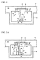
FIG. 1 is a schematic view illustrating a vacuum vapor deposition apparatus including a deposition preventing board having heat reflection suppressor, and an evaporation source cover, according to the invention. -
FIG. 2 is a schematic view illustrating a vacuum vapor deposition apparatus including a deposition preventing board having a plurality of welded fins, according to the invention. -
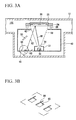
FIG. 3A is a schematic view illustrating a vacuum vapor deposition apparatus including a deposition preventing board having a plurality of fins formed by bending notches, according to the invention. -
FIG. 3B is an enlarged view of the fins formed by bending the notches inFIG. 3A . -
FIG. 4 is a schematic view illustrating a vacuum vapor deposition apparatus including an evaporation source cover having an inclined surface, according to the invention. -
FIG. 5A is a schematic view illustrating a vacuum vapor deposition apparatus to which a corner cube array is given, according to the invention. -
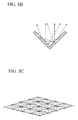
FIG. 5B is a view illustrating the principle of a corner cube. -
FIG. 5C is a view illustrating an enlarged view of the surface of the corner cube array. -
FIG. 6A is a schematic view illustrating a vacuum vapor deposition apparatus including a film thickness sensor covered with a film thickness sensor cover, according to the invention. -
FIG. 6B is a schematic view illustrating a vacuum vapor deposition apparatus including a film thickness sensor cover provided with a tubular hood. -
FIG. 7 is graph in a case where a film formation speed detected by the vacuum vapor deposition apparatus including the heat reflection suppressor according to the invention, a film formation speed detected by the vacuum vapor deposition apparatus that does not include the heat reflection suppressor according to the invention, and an actual film formation speed in a substrate are compared. - Vapor deposition apparatuses of a plurality of embodiments according to the invention will be described below with reference to the drawings. Additionally, a target in the present specification includes a
substrate 20, atray 24, a mask (not illustrated), or the like in the following embodiments. - A vacuum
vapor deposition apparatus 10A according to the invention illustrated inFIG. 1 includes avacuum chamber 12 that is brought into a vacuum atmosphere, and a conveyingroller 28 having a roller that conveys a target into thevacuum chamber 12, and a thin film having a predetermined thickness is formed by vapor-depositing avapor deposition material 38 on the target conveyed at a vapor deposition position within thevacuum chamber 12. In the present embodiment, thesubstrate 20 that is a member to be vapor-deposited is loaded on thetray 24 in a state where amask 26 for vapor-depositing a predetermined range is attached, and thetray 24, themask 26, and thesubstrate 20 are integrally conveyed as the target by the conveyingroller 28. Additionally, the vacuumvapor deposition apparatus 10A includes anevaporation source 30 that discharges the vapor deposition material, an evaporation source cover 32 that surrounds theevaporation source 30, adeposition preventing board 40 that prevents scattering of the dischargedvapor deposition material 38, and afilm thickness sensor 50 that detects the thickness of a film formed of the vapor deposition material. Theevaporation source 30 is disposed to face the target disposed at the vapor deposition position. The evaporation source cover 32 is provided with adischarge port 34 through which the vapor deposition material is discharged, and prevents the vapor deposition material and heat from being scattered other than from thedischarge port 34. Thedeposition preventing board 40 having anopening 42 that exposes thesubstrate 20 to theevaporation source 30, and thefilm thickness sensor 50 that is disposed toward theevaporation source 30 in a space surrounded by the deposition preventing board, is disposed at a position where the vapor deposition of the vapor deposition material to thesubstrate 20 is not hindered, and detects the thickness of the thin film formed of the vapor deposition material are included. - The
film thickness sensor 50 in the present embodiment includes a crystal oscillator. Thefilm thickness sensor 50 measures the resonant frequency of the crystal oscillator. Thevapor deposition material 38 discharged from theevaporation source 30 adheres to the crystal oscillator, a film is formed on a surface of the crystal oscillator, and the resonant frequency changes according to the film thickness of the film. In thefilm thickness sensor 50 in the present embodiment, the film thickness of the film formed of the vapor deposition material is found on the basis of the resonant frequency to be detected, a film formation speed is found on the basis of the time change of the film thickness, and a film formation speed is controlled according to the found film formation speed. - Additionally, the vacuum
vapor deposition apparatus 10A includesheat reflection suppressor 60 that re-reflects the heat which is dissipated from theevaporation source 30 and reflected by the target and suppresses the heat which can be radiated to thefilm thickness sensor 50. In the present embodiment, theheat reflection suppressor 60 is formed with heat absorber by subjecting a blackening treatment to regions on an inner surface of thedeposition preventing board 40 and an outer surface of the evaporation source cover where the heat dissipated from theevaporation source 30 and reflected by the target can be re-reflected toward thefilm thickness sensor 50. Specifically, the blackening treatment is performed, for example, by surface processing, such as plating. - When the
substrate 20 passes above theevaporation source 30, upward heat (H1, H'1) radiated from theevaporation source 30 and heated by a heater is reflected by thesubstrate 20 or the tray 24 (H2, H'2), and is then re-reflected by the evaporation source cover 32 or thedeposition preventing board 40, and a portion (H3, H'3) of the re-reflected heat is radiated to thefilm thickness sensor 50. In this way, as the heat (H3, H'3) re-reflected by the evaporation source cover 32 or thedeposition preventing board 40 is radiated to the film thickness sensor, the temperature change of the crystal oscillator occurs and the resonant frequency changes. Due to the change of the resonant frequency, a film formation speed detected by the film thickness sensor fluctuates even if an actual film formation speed has not changed. The vacuum vapor deposition apparatus also affects the actual film formation speed because the vacuum vapor deposition apparatus attempts to control the film formation speed on the basis of the displaced film formation speed detected by the film thickness sensor. - In the region that has been subjected to the blackening treatment, the re-reflection (H3, H'3) of the heat directed to the
film thickness sensor 50 is suppressed by absorbing the heat (H2, H'2) reflected by thesubstrate 20 that is the target or by thetray 24. Accordingly, when thesubstrate 20 passes through the vapor deposition position above theevaporation source 30, the displacement of the amount of radiant heat that enters the crystal oscillator of thefilm thickness sensor 50 can be suppressed, the measurement error of the film thickness detected by thefilm thickness sensor 50 can be suppressed, and the film formation speed can be more precisely controlled. - A graph obtained by comparing a film formation speed (after a countermeasure) detected by the
film thickness sensor 50 when the above-describedheat reflection suppressor 60 is provided on the inner surface of thedeposition preventing board 40 and on the outer surface of the evaporation source cover, a film formation speed (a non-countermeasure) detected in case of a non-countermeasure, and an actual film formation speed is illustrated inFIG. 7 . When thesubstrate 20 passes above the evaporation source, according to a difference in the shape or material of the target, the heat reflected from the target consisting of thesubstrate 20, thetray 24, and themask 26 changes with time and the re-reflection of the heat received by the film forming sensor similarly changes with time. Although this influences the film formation speed detected by thefilm thickness sensor 50, the change of the film formation speed after the countermeasure is suppressed compared to that in case of the non-countermeasure, and monitoring of a speed closer to the actual film formation speed, that is, a more precise film formation speed, is realized. - Additionally, as the
heat reflection suppressor 60 inFIG. 1 , blast treatment or the like may be provided instead of the blackening treatment. The blast treatment functions as heat diffuser for diffusing the heat (H2, H'2) reflected by thesubstrate 20 or thetray 24, and also functions as heat absorber for absorbing the heat (H2, H'2) reflected by thesubstrate 20 or thetray 24. - According to a second embodiment, the re-reflection (H3, H'3) of the heat that is directed to the
film thickness sensor 50 by diffusing or absorbing the heat (H2, H'2) reflected by thesubstrate 20 or thetray 24 in the inner surface of thedeposition preventing board 40 and the outer surface of the evaporation source cover 32 subjected to the blast treatment can be suppressed. - In addition, similarly, functioning as the heat diffuser and also as the heat absorber is not limited to this blast treatment. For example, the re-reflection (H3, H'3) of the heat directed to the
film thickness sensor 50 may be suppressed by attaching a metallic mesh-like sheet, or a porous sheet formed by roughly sintering a particulate or fibrous metallic material, and by diffusing or absorbing the heat with irregularities provided in the surface of the sheet. - In addition, the
heat reflection suppressor 60 in the first and second embodiments may be given to the whole surface of thedeposition preventing board 40 or the evaporation source cover 32 as illustrated inFIG. 1 , or may be given only to the region that can re-reflect the heat toward thefilm thickness sensor 50. - As illustrated in
FIG. 2 , in a vacuumvapor deposition apparatus 10B of the present embodiment, heat interceptor consisting of a plurality offins 62 fixed to thedeposition preventing board 40 is provided as the heat reflection suppressor. The plurality offins 62 are fixed at a predetermined angle with respect to thedeposition preventing board 40. - Specifically, the plurality of
fins 62 are attached at an angle so that the heat directed to the film thickness sensor by the heat dissipated from theevaporation source 30 and reflected by the target being re-reflected is intercepted and so that the heat reflected by thefins 62 does not enter thefilm thickness sensor 50. In the present embodiment, although the plurality offins 62 are fixed to thedeposition preventing board 40 by welding, the fins may be fixed by another fixing means. - The
fins 62 intercept a portion of the heat re-reflected by thedeposition preventing board 40 in the heat dissipated from theevaporation source 30 and reflected by the target, and suppresses entering of the heat into thefilm thickness sensor 50. Additionally, the heat reflected by the target is re-reflected so as not to enter thefilm thickness sensor 50. Accordingly, the re-reflection (H3) of the heat directed to thefilm thickness sensor 50 can be suppressed by intercepting the heat (H2) reflected by thesubstrate 20 or thetray 24 with thefins 62. - Additionally,
FIG. 3A illustrates a modification example of the third embodiment. As illustrated inFIG. 3A , in the present modification example,fins 64 that are heat interceptor, and through-holes 66 in thedeposition preventing board 40 that are heat transmitter are provided as the heat reflection suppressor. In thedeposition preventing board 40, a plurality offins 64 are formed by bending notches made in a region where the heat dissipated from theevaporation source 30 and reflected by the target can be re-reflected toward thefilm thickness sensor 50, and the through-holes 66 are formed in original portions by forming the fins 64 (refer toFIG. 3B ). In the present modification example, thefins 64, as described above, are bent at an angle such that the heat re-reflected toward thefilm thickness sensor 50 is intercepted and the heat reflected by thefins 64 is re-reflected so as not to enter thefilm thickness sensor 50. - In the present embodiment, similarly, the
fins 64 intercept a portion of the heat re-reflected by thedeposition preventing board 40 in the heat dissipated from theevaporation source 30 and reflected by the target, and suppress entering of the heat into thefilm thickness sensor 50. Additionally, the heat reflected by the target is re-reflected so as not to enter thefilm thickness sensor 50. Moreover, the through-holes 66 formed by bending allow the heat (H2) reflected by thesubstrate 20, thetray 24, or the target to be transmitted to the outside of the space surrounded by thedeposition preventing board 40, and thereby suppress entering of the heat into thefilm thickness sensor 50 through the re-reflection. - In addition, only the through-holes may be provided as the heat reflection suppressor without providing the fins. Additionally, when the
deposition preventing board 40 is provided with the through-holes, it is desirable to provide the through-holes so as to avoid a place where thevapor deposition material 38 can be discharged from thedeposition preventing board 40 into thevacuum chamber 12. - In addition, all of the plurality of
fins film thickness sensor 50. That is, the angle of the plurality offins film thickness sensor 50 in the inner surface of thedeposition preventing board 40 and the outer surface of the evaporation source cover 32 is intercepted, and the heat re-reflected by thefins film thickness sensor 50. - A vacuum
vapor deposition apparatus 10D according to the invention illustrated inFIG. 4 includes an evaporation source cover 32 having aninclined surface 36. Theinclined surface 36 of the evaporation source cover is formed at an angle such that the heat (H2) reflected by the target, such as thesubstrate 20 or thetray 24, is re-reflected in a direction avoiding thefilm thickness sensor 50, and constitutes the heat reflection suppressor in the present embodiment. The evaporation source cover in the present embodiment adopts the pyramidalevaporation source cover 32, and the lateral surface of the evaporation source cover is used as theinclined surface 36 that constitutes the heat reflector. - The angle of the
inclined surface 36 may be appropriately determined so that heat is not re-reflected toward thefilm thickness sensor 50 according to the position of thefilm thickness sensor 50, and the inclined surface may not have a bilaterally symmetrical shape as illustrated inFIG. 3A but may have a bilaterally asymmetrical shape. Additionally, the inclined surface may have a shape such that a horizontal plane or a vertical plane is left behind according to the position of thefilm thickness sensor 50. - Although
FIG. 4 illustrates a form in which theinclined surface 36 is provided at the evaporation source cover 32 to form the heat reflector, the inclined surface may similarly be provided at the deposition preventing board. The heat reflector reflects the heat obtained by the reflected heat H2 from the target being re-reflected by the deposition preventing board toward places other than thefilm thickness sensor 50, thereby suppressing entering of the heat into thefilm thickness sensor 50. - Additionally, as another heat reflector, in a vacuum
vapor deposition apparatus 10E according to the invention illustrated inFIG. 5A , acorner cube array 68, which is heat retro-reflector having a shape as illustrated inFIG. 5C as the heat reflector, is given to regions where the heat dissipated from theevaporation source 30 and reflected by the target can be re-reflected toward thefilm thickness sensor 50, in the inner surface of thedeposition preventing board 40 and the outer surface of the evaporation source cover, instead of providing the inclined surface at the deposition preventing board. - The corner cube reflects the heat, which has entered at an arbitrary angle of incidence, in the same direction as the angle of incidence, as the principle thereof is illustrated in
FIG. 5B . Therefore, if the reflected heat (H2, H'2) from the target is radiated on the surface to which the corner cube array is given, the heat is reflected in the same direction as the direction from which the heat entered. This can prevent the re-reflected heat (H3, H'3) from being radiated toward thefilm thickness sensor 50. - In addition, as well as the corner cube array, general retroreflection processing methods, such as a method using a bead-containing coating material, can be used. Additionally, instead of performing the retroreflection processing on the
deposition preventing board 40 or the evaporation source cover 32 itself, a sheet-like thin plate subjected to the retroreflection processing may be attached to thedeposition preventing board 40 or theevaporation source cover 32. -
FIG. 6A illustrates a vacuumvapor deposition apparatus 10F according to the invention. As illustrated inFIG. 6A , the vacuumvapor deposition apparatus 10F includes a filmthickness sensor cover 52 that covers portions other than a sensor unit of thefilm thickness sensor 50. Accordingly, thefilm thickness sensor 50 can detect film thickness while suppressing radiation of the re-reflected heat to thefilm thickness sensor 50 from the surroundings, and the influence caused by the radiation of the heat from the surroundings can be suppressed so as to control film formation. - Additionally, when the film
thickness sensor cover 52 is attached, the region where the heat (H2) of the evaporation source cover 32 or thedeposition preventing board 40 reflected by the target can be re-reflected and radiated to the film thickness sensor is more narrowly limited. Therefore, the area for providing theheat reflection suppressor 60 can be made small. - Additionally, as illustrated in
FIG. 6B , a tubular hood 54 may be provided at the filmthickness sensor cover 52 in order to further limit the region where the heat of the evaporation source cover 32 or thedeposition preventing board 40 reflected by the target can be re-reflected and radiated to the film thickness sensor (50). The hood 54 limits an angle at which the re-reflected heat can enter the film thickness sensor. Accordingly, the region where the heat of the evaporation source cover 32 or thedeposition preventing board 40 reflected by the target can be re-reflected and radiated to the film thickness sensor is further limited. - Additionally, the aforementioned blackening treatment, blast processing, or retroreflection processing can be performed on the inner surface of the hood 54. By adopting such a configuration, the film formation speed can be more precisely detected by suppressing entering of the heat, which is reflected into the inner surface of the hood 54 in the heat that has entered the hood 54, into the
film thickness sensor 50 and by suppressing the heat that enters thefilm thickness sensor 50. - Although the various embodiments of the invention have been described above as examples, these embodiments may be combined and carried out within a technically possible range so that higher effects are obtained. For example, the blackening process may be performed on the plurality of
fins deposition preventing board 40 may be provided with the plurality offins - In addition, the target in the invention is not limited to the
substrate 20, thetray 24, and themask 26, but refers to an arbitrary structure that can cover theopening 42 of the deposition preventing board, and reflect the heat (H1) dissipated from theevaporation source 30. - In addition, the
heat reflection suppressor 60 according to the invention are not limited to being provided at the evaporation source cover 32 and thedeposition preventing board 40, but may be provided on the surface of an arbitrary structure that is disposed within a space surrounded by thedeposition preventing board 40. - Although the various embodiments of the vacuum vapor deposition apparatus according to the invention have been described so far, the vapor deposition apparatus of the invention is not limited to the aforementioned respective embodiments, but appropriate modifications, improvements, or the like can be made. For example, by disposing a temperature sensor that measures the temperature of the
film thickness sensor 50, and using the correction of the film formation speed together depending on the monitoring of a temperature change, it is possible to more precisely control the film formation speed. - The invention according to the vacuum vapor deposition apparatus that can suppress the temperature change of the film thickness sensor caused by the reflected heat from the target, to more precisely control the film formation speed.
-
- 10A, 10B, 10C, 10D, 10E, 10F, 10G: VACUUM VAPOR DEPOSITION APPARATUS
- 12: VACUUM CHAMBER
- 20: SUBSTRATE
- 24: TRAY
- 26: MASK
- 28: CONVEYING ROLLER
- 30: EVAPORATION SOURCE
- 32, 33: EVAPORATION SOURCE COVER
- 34: DISCHARGE PORT
- 36: INCLINED SURFACE
- 38: VAPOR DEPOSITION MATERIAL
- 40: DEPOSITION PREVENTING BOARD
- 42: OPENING
- 50: FILM THICKNESS SENSOR
- 52: FILM THICKNESS SENSOR COVER
- 54: HOOD
- 60: HEAT REFLECTION SUPPRESSOR
- 62, 64: FIN
- 66: THROUGH HOLE
- 68: CORNER CUBE ARRAY
- H1, H'1: HEAT FROM EVAPORATION SOURCE
- H2, H'2: HEAT REFLECTED BY TARGET
- H3, H'3, H4: RE-REFLECTED HEAT
Claims (16)
- A vacuum vapor deposition apparatus comprising:an evaporation source that is disposed so that a vapor deposition material is discharged toward a position where a target is disposed;an evaporation source cover that surrounds the evaporation source and has a discharge port through which the vapor deposition material is discharged;a deposition preventing board that is disposed around the evaporation source cover to prevent scattering of the vapor deposition material, and has an opening through which the target is exposed to the evaporation source;a film thickness sensor that is arranged in a space surrounded by the deposition preventing board and detects the thickness of a film formed of the vapor deposition material discharged from the evaporation source; andheat reflection suppressor that is provided at a position where heat radiated from the evaporation source and reflected by the target is capable of being re-reflected and radiated to the film thickness sensor and suppresses heat which is capable of being radiated to the film thickness sensor.
- The vacuum vapor deposition apparatus according to Claim 1,
wherein the heat reflection suppressor includes heat absorber for absorbing the heat reflected by the target. - The vacuum vapor deposition apparatus according to Claim 1 or 2, wherein the heat reflection suppressor includes heat diffuser for diffusing the heat reflected by the target.
- The vacuum vapor deposition apparatus according to any one of Claims 1 to 3,
wherein the heat reflection suppressor includes heat interceptor for intercepting the heat reflected by the target. - The vacuum vapor deposition apparatus according to any one of Claims 1 to 4,
wherein the heat reflection suppressor includes heat transmitter for allowing the heat reflected by the target to be transmitted therethrough. - The vacuum vapor deposition apparatus according to any one of Claims 1 to 5,
wherein the heat reflection suppressor includes heat reflector for reflecting the heat reflected by the target in a direction avoiding the film thickness sensor. - The vacuum vapor deposition apparatus according to any one of Claims 1 to 6,
wherein the heat reflection suppressor includes heat retro-reflector for returning the heat reflected from the target in a direction from which the heat entered. - The vacuum vapor deposition apparatus according to any one of Claims 1 to 7, further comprising:a film thickness sensor cover that surrounds at least a portion of the film thickness sensor.
- The vacuum vapor deposition apparatus according to Claim 2, wherein the heat absorber is obtained by a blackening treatment.
- The vacuum vapor deposition apparatus according to Claim 3, wherein the heat diffuser is obtained by blast processing.
- The vacuum vapor deposition apparatus according to Claim 2, wherein the heat absorber is obtained by blast processing.
- The vacuum vapor deposition apparatus according to Claim 4, wherein the heat interceptor includes at least one fin attached to the deposition preventing board.
- The vacuum vapor deposition apparatus according to Claim 5, wherein the heat transmitter includes a through-hole formed in the deposition preventing board.
- The vacuum vapor deposition apparatus according to Claim 6, wherein the heat reflector includes an inclined surface that is provided at the evaporation source cover and is formed at an angle such that the heat reflected by the target is reflected in a direction avoiding the film thickness sensor.
- The vacuum vapor deposition apparatus according to Claim 7, wherein the heat retro-reflector has a corner cube array or a bead-containing coating material.
- The vacuum vapor deposition apparatus according to Claim 8, wherein the film thickness sensor cover includes a tubular hood of which an inner surface is blackened.
Applications Claiming Priority (1)
| Application Number | Priority Date | Filing Date | Title |
|---|---|---|---|
| PCT/JP2012/079420 WO2014076770A1 (en) | 2012-11-13 | 2012-11-13 | Vacuum vapor deposition apparatus |
Publications (3)
| Publication Number | Publication Date |
|---|---|
| EP2921571A1 true EP2921571A1 (en) | 2015-09-23 |
| EP2921571A4 EP2921571A4 (en) | 2015-12-23 |
| EP2921571B1 EP2921571B1 (en) | 2017-02-01 |
Family
ID=50730712
Family Applications (1)
| Application Number | Title | Priority Date | Filing Date |
|---|---|---|---|
| EP12888566.2A Not-in-force EP2921571B1 (en) | 2012-11-13 | 2012-11-13 | Vacuum vapor deposition apparatus |
Country Status (5)
| Country | Link |
|---|---|
| EP (1) | EP2921571B1 (en) |
| JP (1) | JP5916883B2 (en) |
| KR (1) | KR101643107B1 (en) |
| CN (1) | CN104508172B (en) |
| WO (1) | WO2014076770A1 (en) |
Cited By (1)
| Publication number | Priority date | Publication date | Assignee | Title |
|---|---|---|---|---|
| CN105486215A (en) * | 2015-12-15 | 2016-04-13 | 苏州晶鼎鑫光电科技有限公司 | Plated film thickness monitoring method |
Families Citing this family (6)
| Publication number | Priority date | Publication date | Assignee | Title |
|---|---|---|---|---|
| JP6277883B2 (en) * | 2014-06-20 | 2018-02-14 | コニカミノルタ株式会社 | Method and apparatus for producing gas barrier film |
| WO2020017047A1 (en) * | 2018-07-20 | 2020-01-23 | シャープ株式会社 | Vapor deposition apparatus |
| CN110453181A (en) * | 2019-08-08 | 2019-11-15 | 深圳市华星光电半导体显示技术有限公司 | Evaporated device and its prevent plate |
| CN110819940B (en) * | 2019-11-29 | 2024-04-16 | 福建华佳彩有限公司 | A vapor deposition mechanism |
| KR102458164B1 (en) | 2020-11-05 | 2022-10-24 | (주)제이피오토메이션 | Vacuum evaporation device with anti-pollution shield plate |
| JP7503481B2 (en) * | 2020-11-17 | 2024-06-20 | 株式会社アルバック | Film Thickness Monitor |
Family Cites Families (19)
| Publication number | Priority date | Publication date | Assignee | Title |
|---|---|---|---|---|
| JPS6093303A (en) | 1983-10-27 | 1985-05-25 | Anelva Corp | Quartz-type thickness monitor |
| JPH03150365A (en) * | 1989-07-26 | 1991-06-26 | Tokyo Electron Ltd | Heat treating device |
| JP3413626B2 (en) * | 1994-07-22 | 2003-06-03 | 日本カーバイド工業株式会社 | Manufacturing method of retroreflective sheet |
| US5770124A (en) * | 1996-04-30 | 1998-06-23 | Minnesota Mining And Manufacturing Company | Method of making glittering cube-corner retroreflective sheeting |
| JPH1025563A (en) * | 1996-07-08 | 1998-01-27 | Shinko Seiki Co Ltd | Vacuum depositing device and vacuum depositing method |
| JP4195205B2 (en) * | 2001-03-16 | 2008-12-10 | 三井化学株式会社 | Preparation method of organic polymer thin film |
| JP4490160B2 (en) * | 2004-05-13 | 2010-06-23 | 株式会社アルバック | Organic thin film deposition system |
| JP4552184B2 (en) * | 2004-10-22 | 2010-09-29 | 富士電機ホールディングス株式会社 | Apparatus and method for depositing organic layer on substrate for organic light emitting device |
| KR20060081015A (en) * | 2005-01-06 | 2006-07-12 | 삼성에스디아이 주식회사 | Vacuum evaporator |
| JP2007077419A (en) * | 2005-09-12 | 2007-03-29 | Seiko Epson Corp | Film thickness measuring apparatus and thin film forming apparatus |
| JP2007297704A (en) * | 2006-04-05 | 2007-11-15 | Seiko Epson Corp | Vapor deposition apparatus, vapor deposition method, electro-optical device manufacturing method, and film forming apparatus |
| JP2008276998A (en) * | 2007-04-26 | 2008-11-13 | Sony Corp | Film thickness sensor, thin film forming apparatus, organic EL display device manufacturing apparatus, and organic EL display device manufacturing method |
| JP5252864B2 (en) * | 2007-09-10 | 2013-07-31 | キヤノン株式会社 | Organic EL display panel manufacturing equipment |
| JP4974858B2 (en) * | 2007-11-19 | 2012-07-11 | 株式会社アルバック | Film forming apparatus and thin film forming method |
| KR101006952B1 (en) * | 2008-04-25 | 2011-01-12 | (주)알파플러스 | Vacuum evaporation source device for thin film production |
| JP2012012689A (en) * | 2010-07-05 | 2012-01-19 | Canon Inc | Method and apparatus for vacuum evaporation |
| JP5456711B2 (en) * | 2011-03-03 | 2014-04-02 | 住友重機械工業株式会社 | Deposition equipment |
| JP2013104085A (en) * | 2011-11-11 | 2013-05-30 | Hitachi Zosen Corp | Film thickness sensor device for electron beam deposition |
| JP2014055342A (en) * | 2012-09-14 | 2014-03-27 | Hitachi High-Technologies Corp | Film deposition apparatus |
-
2012
- 2012-11-13 JP JP2014546762A patent/JP5916883B2/en active Active
- 2012-11-13 EP EP12888566.2A patent/EP2921571B1/en not_active Not-in-force
- 2012-11-13 WO PCT/JP2012/079420 patent/WO2014076770A1/en not_active Ceased
- 2012-11-13 KR KR1020157000967A patent/KR101643107B1/en not_active Expired - Fee Related
- 2012-11-13 CN CN201280075029.5A patent/CN104508172B/en not_active Expired - Fee Related
Cited By (1)
| Publication number | Priority date | Publication date | Assignee | Title |
|---|---|---|---|---|
| CN105486215A (en) * | 2015-12-15 | 2016-04-13 | 苏州晶鼎鑫光电科技有限公司 | Plated film thickness monitoring method |
Also Published As
| Publication number | Publication date |
|---|---|
| CN104508172B (en) | 2016-10-12 |
| EP2921571B1 (en) | 2017-02-01 |
| CN104508172A (en) | 2015-04-08 |
| JP5916883B2 (en) | 2016-05-11 |
| EP2921571A4 (en) | 2015-12-23 |
| KR101643107B1 (en) | 2016-07-26 |
| KR20150018885A (en) | 2015-02-24 |
| JPWO2014076770A1 (en) | 2016-09-08 |
| WO2014076770A1 (en) | 2014-05-22 |
Similar Documents
| Publication | Publication Date | Title |
|---|---|---|
| EP2921571B1 (en) | Vacuum vapor deposition apparatus | |
| TWI477624B (en) | Film forming device | |
| EP2642822B1 (en) | Infrared ray detecting apparatus and heating cooker having the same | |
| CN107574411B (en) | Evaporation device and evaporation source | |
| JP6549951B2 (en) | Structure mounted with radar device, method of mounting radar device, and bracket | |
| CN111725116B (en) | Loading cavity and wafer distribution status detection method in semiconductor equipment | |
| KR20150117617A (en) | Susceptor with radiation source compensation | |
| KR20160090987A (en) | Deposition rate measuring apparatus | |
| JPH0854211A (en) | Method and apparatus for monitoring deposition rate of opaque film | |
| CN101603169B (en) | Film plating device | |
| EP2695968A1 (en) | Deposition apparatus and method of measuring the deposition material in it | |
| US20210247322A1 (en) | Measuring apparatus and film forming apparatus | |
| JP6532800B2 (en) | Antireflection member and orienter device | |
| CA2837305A1 (en) | Quantum harmonic radar | |
| CN113990783B (en) | A wafer level buffer device | |
| KR20160035534A (en) | Method and apparatus for forming an EMI-shielding layer using a sputtering process | |
| JP2013511619A (en) | Apparatus and method for coating a substrate | |
| KR101582670B1 (en) | Evaporation-rate monitoring module for vacuum effusion cell | |
| US8497974B2 (en) | Exhaust apparatus, processing apparatus, and device manufacturing method | |
| JP5927652B2 (en) | Optical monitor and vacuum deposition apparatus using the same | |
| US20130014700A1 (en) | Target shield designs in multi-target deposition system. | |
| US20070129827A1 (en) | High temperature optical sensor device for substrate fabrication equipment | |
| JP6481435B2 (en) | Optical device | |
| JP2008138261A (en) | Vacuum deposition apparatus and method therefor | |
| KR102339795B1 (en) | Movable Masking Element |
Legal Events
| Date | Code | Title | Description |
|---|---|---|---|
| PUAI | Public reference made under article 153(3) epc to a published international application that has entered the european phase |
Free format text: ORIGINAL CODE: 0009012 |
|
| 17P | Request for examination filed |
Effective date: 20150204 |
|
| AK | Designated contracting states |
Kind code of ref document: A1 Designated state(s): AL AT BE BG CH CY CZ DE DK EE ES FI FR GB GR HR HU IE IS IT LI LT LU LV MC MK MT NL NO PL PT RO RS SE SI SK SM TR |
|
| AX | Request for extension of the european patent |
Extension state: BA ME |
|
| RA4 | Supplementary search report drawn up and despatched (corrected) |
Effective date: 20151123 |
|
| RIC1 | Information provided on ipc code assigned before grant |
Ipc: C23C 14/24 20060101AFI20151117BHEP |
|
| DAX | Request for extension of the european patent (deleted) | ||
| GRAP | Despatch of communication of intention to grant a patent |
Free format text: ORIGINAL CODE: EPIDOSNIGR1 |
|
| INTG | Intention to grant announced |
Effective date: 20160919 |
|
| RIN1 | Information on inventor provided before grant (corrected) |
Inventor name: SHIGEOKA, NOBUYUKI |
|
| GRAS | Grant fee paid |
Free format text: ORIGINAL CODE: EPIDOSNIGR3 |
|
| GRAA | (expected) grant |
Free format text: ORIGINAL CODE: 0009210 |
|
| AK | Designated contracting states |
Kind code of ref document: B1 Designated state(s): AL AT BE BG CH CY CZ DE DK EE ES FI FR GB GR HR HU IE IS IT LI LT LU LV MC MK MT NL NO PL PT RO RS SE SI SK SM TR |
|
| REG | Reference to a national code |
Ref country code: GB Ref legal event code: FG4D |
|
| REG | Reference to a national code |
Ref country code: CH Ref legal event code: EP Ref country code: AT Ref legal event code: REF Ref document number: 865676 Country of ref document: AT Kind code of ref document: T Effective date: 20170215 |
|
| REG | Reference to a national code |
Ref country code: IE Ref legal event code: FG4D |
|
| REG | Reference to a national code |
Ref country code: NL Ref legal event code: FP |
|
| REG | Reference to a national code |
Ref country code: DE Ref legal event code: R096 Ref document number: 602012028500 Country of ref document: DE |
|
| REG | Reference to a national code |
Ref country code: LT Ref legal event code: MG4D |
|
| REG | Reference to a national code |
Ref country code: AT Ref legal event code: MK05 Ref document number: 865676 Country of ref document: AT Kind code of ref document: T Effective date: 20170201 |
|
| PG25 | Lapsed in a contracting state [announced via postgrant information from national office to epo] |
Ref country code: GR Free format text: LAPSE BECAUSE OF FAILURE TO SUBMIT A TRANSLATION OF THE DESCRIPTION OR TO PAY THE FEE WITHIN THE PRESCRIBED TIME-LIMIT Effective date: 20170502 Ref country code: IS Free format text: LAPSE BECAUSE OF FAILURE TO SUBMIT A TRANSLATION OF THE DESCRIPTION OR TO PAY THE FEE WITHIN THE PRESCRIBED TIME-LIMIT Effective date: 20170601 Ref country code: HR Free format text: LAPSE BECAUSE OF FAILURE TO SUBMIT A TRANSLATION OF THE DESCRIPTION OR TO PAY THE FEE WITHIN THE PRESCRIBED TIME-LIMIT Effective date: 20170201 Ref country code: NO Free format text: LAPSE BECAUSE OF FAILURE TO SUBMIT A TRANSLATION OF THE DESCRIPTION OR TO PAY THE FEE WITHIN THE PRESCRIBED TIME-LIMIT Effective date: 20170501 Ref country code: LT Free format text: LAPSE BECAUSE OF FAILURE TO SUBMIT A TRANSLATION OF THE DESCRIPTION OR TO PAY THE FEE WITHIN THE PRESCRIBED TIME-LIMIT Effective date: 20170201 Ref country code: FI Free format text: LAPSE BECAUSE OF FAILURE TO SUBMIT A TRANSLATION OF THE DESCRIPTION OR TO PAY THE FEE WITHIN THE PRESCRIBED TIME-LIMIT Effective date: 20170201 |
|
| PG25 | Lapsed in a contracting state [announced via postgrant information from national office to epo] |
Ref country code: SE Free format text: LAPSE BECAUSE OF FAILURE TO SUBMIT A TRANSLATION OF THE DESCRIPTION OR TO PAY THE FEE WITHIN THE PRESCRIBED TIME-LIMIT Effective date: 20170201 Ref country code: ES Free format text: LAPSE BECAUSE OF FAILURE TO SUBMIT A TRANSLATION OF THE DESCRIPTION OR TO PAY THE FEE WITHIN THE PRESCRIBED TIME-LIMIT Effective date: 20170201 Ref country code: PL Free format text: LAPSE BECAUSE OF FAILURE TO SUBMIT A TRANSLATION OF THE DESCRIPTION OR TO PAY THE FEE WITHIN THE PRESCRIBED TIME-LIMIT Effective date: 20170201 Ref country code: AT Free format text: LAPSE BECAUSE OF FAILURE TO SUBMIT A TRANSLATION OF THE DESCRIPTION OR TO PAY THE FEE WITHIN THE PRESCRIBED TIME-LIMIT Effective date: 20170201 Ref country code: RS Free format text: LAPSE BECAUSE OF FAILURE TO SUBMIT A TRANSLATION OF THE DESCRIPTION OR TO PAY THE FEE WITHIN THE PRESCRIBED TIME-LIMIT Effective date: 20170201 Ref country code: PT Free format text: LAPSE BECAUSE OF FAILURE TO SUBMIT A TRANSLATION OF THE DESCRIPTION OR TO PAY THE FEE WITHIN THE PRESCRIBED TIME-LIMIT Effective date: 20170601 Ref country code: LV Free format text: LAPSE BECAUSE OF FAILURE TO SUBMIT A TRANSLATION OF THE DESCRIPTION OR TO PAY THE FEE WITHIN THE PRESCRIBED TIME-LIMIT Effective date: 20170201 Ref country code: BG Free format text: LAPSE BECAUSE OF FAILURE TO SUBMIT A TRANSLATION OF THE DESCRIPTION OR TO PAY THE FEE WITHIN THE PRESCRIBED TIME-LIMIT Effective date: 20170501 |
|
| PG25 | Lapsed in a contracting state [announced via postgrant information from national office to epo] |
Ref country code: RO Free format text: LAPSE BECAUSE OF FAILURE TO SUBMIT A TRANSLATION OF THE DESCRIPTION OR TO PAY THE FEE WITHIN THE PRESCRIBED TIME-LIMIT Effective date: 20170201 Ref country code: CZ Free format text: LAPSE BECAUSE OF FAILURE TO SUBMIT A TRANSLATION OF THE DESCRIPTION OR TO PAY THE FEE WITHIN THE PRESCRIBED TIME-LIMIT Effective date: 20170201 Ref country code: IT Free format text: LAPSE BECAUSE OF FAILURE TO SUBMIT A TRANSLATION OF THE DESCRIPTION OR TO PAY THE FEE WITHIN THE PRESCRIBED TIME-LIMIT Effective date: 20170201 Ref country code: EE Free format text: LAPSE BECAUSE OF FAILURE TO SUBMIT A TRANSLATION OF THE DESCRIPTION OR TO PAY THE FEE WITHIN THE PRESCRIBED TIME-LIMIT Effective date: 20170201 Ref country code: SK Free format text: LAPSE BECAUSE OF FAILURE TO SUBMIT A TRANSLATION OF THE DESCRIPTION OR TO PAY THE FEE WITHIN THE PRESCRIBED TIME-LIMIT Effective date: 20170201 |
|
| REG | Reference to a national code |
Ref country code: DE Ref legal event code: R097 Ref document number: 602012028500 Country of ref document: DE |
|
| PG25 | Lapsed in a contracting state [announced via postgrant information from national office to epo] |
Ref country code: DK Free format text: LAPSE BECAUSE OF FAILURE TO SUBMIT A TRANSLATION OF THE DESCRIPTION OR TO PAY THE FEE WITHIN THE PRESCRIBED TIME-LIMIT Effective date: 20170201 Ref country code: SM Free format text: LAPSE BECAUSE OF FAILURE TO SUBMIT A TRANSLATION OF THE DESCRIPTION OR TO PAY THE FEE WITHIN THE PRESCRIBED TIME-LIMIT Effective date: 20170201 |
|
| PLBE | No opposition filed within time limit |
Free format text: ORIGINAL CODE: 0009261 |
|
| STAA | Information on the status of an ep patent application or granted ep patent |
Free format text: STATUS: NO OPPOSITION FILED WITHIN TIME LIMIT |
|
| 26N | No opposition filed |
Effective date: 20171103 |
|
| PG25 | Lapsed in a contracting state [announced via postgrant information from national office to epo] |
Ref country code: SI Free format text: LAPSE BECAUSE OF FAILURE TO SUBMIT A TRANSLATION OF THE DESCRIPTION OR TO PAY THE FEE WITHIN THE PRESCRIBED TIME-LIMIT Effective date: 20170201 |
|
| PG25 | Lapsed in a contracting state [announced via postgrant information from national office to epo] |
Ref country code: MC Free format text: LAPSE BECAUSE OF FAILURE TO SUBMIT A TRANSLATION OF THE DESCRIPTION OR TO PAY THE FEE WITHIN THE PRESCRIBED TIME-LIMIT Effective date: 20170201 |
|
| GBPC | Gb: european patent ceased through non-payment of renewal fee |
Effective date: 20171113 |
|
| PG25 | Lapsed in a contracting state [announced via postgrant information from national office to epo] |
Ref country code: LI Free format text: LAPSE BECAUSE OF NON-PAYMENT OF DUE FEES Effective date: 20171130 Ref country code: CH Free format text: LAPSE BECAUSE OF NON-PAYMENT OF DUE FEES Effective date: 20171130 |
|
| PG25 | Lapsed in a contracting state [announced via postgrant information from national office to epo] |
Ref country code: LU Free format text: LAPSE BECAUSE OF NON-PAYMENT OF DUE FEES Effective date: 20171113 |
|
| REG | Reference to a national code |
Ref country code: FR Ref legal event code: ST Effective date: 20180731 Ref country code: BE Ref legal event code: MM Effective date: 20171130 |
|
| REG | Reference to a national code |
Ref country code: IE Ref legal event code: MM4A |
|
| PG25 | Lapsed in a contracting state [announced via postgrant information from national office to epo] |
Ref country code: MT Free format text: LAPSE BECAUSE OF NON-PAYMENT OF DUE FEES Effective date: 20171113 |
|
| PG25 | Lapsed in a contracting state [announced via postgrant information from national office to epo] |
Ref country code: FR Free format text: LAPSE BECAUSE OF NON-PAYMENT OF DUE FEES Effective date: 20171130 Ref country code: IE Free format text: LAPSE BECAUSE OF NON-PAYMENT OF DUE FEES Effective date: 20171113 |
|
| PG25 | Lapsed in a contracting state [announced via postgrant information from national office to epo] |
Ref country code: GB Free format text: LAPSE BECAUSE OF NON-PAYMENT OF DUE FEES Effective date: 20171113 Ref country code: BE Free format text: LAPSE BECAUSE OF NON-PAYMENT OF DUE FEES Effective date: 20171130 |
|
| PG25 | Lapsed in a contracting state [announced via postgrant information from national office to epo] |
Ref country code: HU Free format text: LAPSE BECAUSE OF FAILURE TO SUBMIT A TRANSLATION OF THE DESCRIPTION OR TO PAY THE FEE WITHIN THE PRESCRIBED TIME-LIMIT; INVALID AB INITIO Effective date: 20121113 |
|
| PG25 | Lapsed in a contracting state [announced via postgrant information from national office to epo] |
Ref country code: CY Free format text: LAPSE BECAUSE OF FAILURE TO SUBMIT A TRANSLATION OF THE DESCRIPTION OR TO PAY THE FEE WITHIN THE PRESCRIBED TIME-LIMIT Effective date: 20170201 |
|
| PG25 | Lapsed in a contracting state [announced via postgrant information from national office to epo] |
Ref country code: MK Free format text: LAPSE BECAUSE OF FAILURE TO SUBMIT A TRANSLATION OF THE DESCRIPTION OR TO PAY THE FEE WITHIN THE PRESCRIBED TIME-LIMIT Effective date: 20170201 |
|
| PG25 | Lapsed in a contracting state [announced via postgrant information from national office to epo] |
Ref country code: TR Free format text: LAPSE BECAUSE OF FAILURE TO SUBMIT A TRANSLATION OF THE DESCRIPTION OR TO PAY THE FEE WITHIN THE PRESCRIBED TIME-LIMIT Effective date: 20170201 |
|
| PG25 | Lapsed in a contracting state [announced via postgrant information from national office to epo] |
Ref country code: AL Free format text: LAPSE BECAUSE OF FAILURE TO SUBMIT A TRANSLATION OF THE DESCRIPTION OR TO PAY THE FEE WITHIN THE PRESCRIBED TIME-LIMIT Effective date: 20170201 |
|
| PGFP | Annual fee paid to national office [announced via postgrant information from national office to epo] |
Ref country code: NL Payment date: 20201015 Year of fee payment: 9 |
|
| PGFP | Annual fee paid to national office [announced via postgrant information from national office to epo] |
Ref country code: DE Payment date: 20201103 Year of fee payment: 9 |
|
| REG | Reference to a national code |
Ref country code: DE Ref legal event code: R119 Ref document number: 602012028500 Country of ref document: DE |
|
| REG | Reference to a national code |
Ref country code: NL Ref legal event code: MM Effective date: 20211201 |
|
| PG25 | Lapsed in a contracting state [announced via postgrant information from national office to epo] |
Ref country code: NL Free format text: LAPSE BECAUSE OF NON-PAYMENT OF DUE FEES Effective date: 20211201 |
|
| PG25 | Lapsed in a contracting state [announced via postgrant information from national office to epo] |
Ref country code: DE Free format text: LAPSE BECAUSE OF NON-PAYMENT OF DUE FEES Effective date: 20220601 |