EP2917766B1 - Sub-band infra-red irradiation for detector crystals - Google Patents
Sub-band infra-red irradiation for detector crystals Download PDFInfo
- Publication number
- EP2917766B1 EP2917766B1 EP13799686.4A EP13799686A EP2917766B1 EP 2917766 B1 EP2917766 B1 EP 2917766B1 EP 13799686 A EP13799686 A EP 13799686A EP 2917766 B1 EP2917766 B1 EP 2917766B1
- Authority
- EP
- European Patent Office
- Prior art keywords
- semiconductor layer
- infrared
- radiation
- directly converting
- sources
- Prior art date
- Legal status (The legal status is an assumption and is not a legal conclusion. Google has not performed a legal analysis and makes no representation as to the accuracy of the status listed.)
- Active
Links
- 239000013078 crystal Substances 0.000 title claims description 18
- 230000005855 radiation Effects 0.000 claims description 61
- 239000004065 semiconductor Substances 0.000 claims description 39
- 239000000758 substrate Substances 0.000 claims description 10
- 238000004519 manufacturing process Methods 0.000 claims description 8
- 238000000034 method Methods 0.000 claims description 4
- 238000012360 testing method Methods 0.000 claims description 3
- 229910004611 CdZnTe Inorganic materials 0.000 description 23
- 239000000463 material Substances 0.000 description 20
- 238000006243 chemical reaction Methods 0.000 description 10
- 238000001465 metallisation Methods 0.000 description 8
- 230000010287 polarization Effects 0.000 description 8
- 238000005259 measurement Methods 0.000 description 7
- 238000005286 illumination Methods 0.000 description 6
- 238000001514 detection method Methods 0.000 description 5
- 230000005684 electric field Effects 0.000 description 5
- 239000002800 charge carrier Substances 0.000 description 4
- 229910004613 CdTe Inorganic materials 0.000 description 3
- 238000010521 absorption reaction Methods 0.000 description 3
- 230000005516 deep trap Effects 0.000 description 3
- 230000007547 defect Effects 0.000 description 3
- 230000001419 dependent effect Effects 0.000 description 3
- 238000010586 diagram Methods 0.000 description 3
- 230000000694 effects Effects 0.000 description 3
- 238000005516 engineering process Methods 0.000 description 3
- 238000011156 evaluation Methods 0.000 description 3
- 238000004806 packaging method and process Methods 0.000 description 3
- 230000035508 accumulation Effects 0.000 description 2
- 238000009825 accumulation Methods 0.000 description 2
- 230000004888 barrier function Effects 0.000 description 2
- 230000008901 benefit Effects 0.000 description 2
- 238000002059 diagnostic imaging Methods 0.000 description 2
- 230000004907 flux Effects 0.000 description 2
- 229910000679 solder Inorganic materials 0.000 description 2
- 229910000980 Aluminium gallium arsenide Inorganic materials 0.000 description 1
- 229910001218 Gallium arsenide Inorganic materials 0.000 description 1
- 238000003491 array Methods 0.000 description 1
- 230000015572 biosynthetic process Effects 0.000 description 1
- 230000008859 change Effects 0.000 description 1
- 230000000295 complement effect Effects 0.000 description 1
- 238000002591 computed tomography Methods 0.000 description 1
- 238000013016 damping Methods 0.000 description 1
- 230000005670 electromagnetic radiation Effects 0.000 description 1
- 238000002474 experimental method Methods 0.000 description 1
- 230000002349 favourable effect Effects 0.000 description 1
- 230000005251 gamma ray Effects 0.000 description 1
- 239000002223 garnet Substances 0.000 description 1
- 229910052732 germanium Inorganic materials 0.000 description 1
- GNPVGFCGXDBREM-UHFFFAOYSA-N germanium atom Chemical compound [Ge] GNPVGFCGXDBREM-UHFFFAOYSA-N 0.000 description 1
- 230000010354 integration Effects 0.000 description 1
- 230000003993 interaction Effects 0.000 description 1
- 230000005865 ionizing radiation Effects 0.000 description 1
- 238000004020 luminiscence type Methods 0.000 description 1
- 239000011159 matrix material Substances 0.000 description 1
- 229910044991 metal oxide Inorganic materials 0.000 description 1
- 150000004706 metal oxides Chemical class 0.000 description 1
- 230000003287 optical effect Effects 0.000 description 1
- 238000012856 packing Methods 0.000 description 1
- 230000003094 perturbing effect Effects 0.000 description 1
- 230000010399 physical interaction Effects 0.000 description 1
- 230000008569 process Effects 0.000 description 1
- 238000012545 processing Methods 0.000 description 1
- 229910052710 silicon Inorganic materials 0.000 description 1
- 239000010703 silicon Substances 0.000 description 1
- 230000003595 spectral effect Effects 0.000 description 1
- 238000001228 spectrum Methods 0.000 description 1
- 239000000126 substance Substances 0.000 description 1
Images


Classifications
-
- G—PHYSICS
- G01—MEASURING; TESTING
- G01J—MEASUREMENT OF INTENSITY, VELOCITY, SPECTRAL CONTENT, POLARISATION, PHASE OR PULSE CHARACTERISTICS OF INFRARED, VISIBLE OR ULTRAVIOLET LIGHT; COLORIMETRY; RADIATION PYROMETRY
- G01J1/00—Photometry, e.g. photographic exposure meter
- G01J1/42—Photometry, e.g. photographic exposure meter using electric radiation detectors
- G01J1/44—Electric circuits
-
- G—PHYSICS
- G01—MEASURING; TESTING
- G01T—MEASUREMENT OF NUCLEAR OR X-RADIATION
- G01T1/00—Measuring X-radiation, gamma radiation, corpuscular radiation, or cosmic radiation
-
- G—PHYSICS
- G01—MEASURING; TESTING
- G01T—MEASUREMENT OF NUCLEAR OR X-RADIATION
- G01T1/00—Measuring X-radiation, gamma radiation, corpuscular radiation, or cosmic radiation
- G01T1/16—Measuring radiation intensity
- G01T1/24—Measuring radiation intensity with semiconductor detectors
-
- H—ELECTRICITY
- H10—SEMICONDUCTOR DEVICES; ELECTRIC SOLID-STATE DEVICES NOT OTHERWISE PROVIDED FOR
- H10F—INORGANIC SEMICONDUCTOR DEVICES SENSITIVE TO INFRARED RADIATION, LIGHT, ELECTROMAGNETIC RADIATION OF SHORTER WAVELENGTH OR CORPUSCULAR RADIATION
- H10F30/00—Individual radiation-sensitive semiconductor devices in which radiation controls the flow of current through the devices, e.g. photodetectors
- H10F30/10—Individual radiation-sensitive semiconductor devices in which radiation controls the flow of current through the devices, e.g. photodetectors the devices being sensitive to infrared radiation, visible or ultraviolet radiation, and having no potential barriers, e.g. photoresistors
-
- H—ELECTRICITY
- H10—SEMICONDUCTOR DEVICES; ELECTRIC SOLID-STATE DEVICES NOT OTHERWISE PROVIDED FOR
- H10F—INORGANIC SEMICONDUCTOR DEVICES SENSITIVE TO INFRARED RADIATION, LIGHT, ELECTROMAGNETIC RADIATION OF SHORTER WAVELENGTH OR CORPUSCULAR RADIATION
- H10F30/00—Individual radiation-sensitive semiconductor devices in which radiation controls the flow of current through the devices, e.g. photodetectors
- H10F30/301—Individual radiation-sensitive semiconductor devices in which radiation controls the flow of current through the devices, e.g. photodetectors the devices being sensitive to very short wavelength, e.g. being sensitive to X-rays, gamma-rays or corpuscular radiation
-
- H—ELECTRICITY
- H10—SEMICONDUCTOR DEVICES; ELECTRIC SOLID-STATE DEVICES NOT OTHERWISE PROVIDED FOR
- H10F—INORGANIC SEMICONDUCTOR DEVICES SENSITIVE TO INFRARED RADIATION, LIGHT, ELECTROMAGNETIC RADIATION OF SHORTER WAVELENGTH OR CORPUSCULAR RADIATION
- H10F71/00—Manufacture or treatment of devices covered by this subclass
- H10F71/125—The active layers comprising only Group II-VI materials, e.g. CdS, ZnS or CdTe
- H10F71/1253—The active layers comprising only Group II-VI materials, e.g. CdS, ZnS or CdTe comprising at least three elements, e.g. HgCdTe
-
- H—ELECTRICITY
- H10—SEMICONDUCTOR DEVICES; ELECTRIC SOLID-STATE DEVICES NOT OTHERWISE PROVIDED FOR
- H10F—INORGANIC SEMICONDUCTOR DEVICES SENSITIVE TO INFRARED RADIATION, LIGHT, ELECTROMAGNETIC RADIATION OF SHORTER WAVELENGTH OR CORPUSCULAR RADIATION
- H10F77/00—Constructional details of devices covered by this subclass
- H10F77/10—Semiconductor bodies
- H10F77/12—Active materials
- H10F77/123—Active materials comprising only Group II-VI materials, e.g. CdS, ZnS or HgCdTe
- H10F77/1237—Active materials comprising only Group II-VI materials, e.g. CdS, ZnS or HgCdTe having at least three elements, e.g. HgCdTe
-
- G—PHYSICS
- G01—MEASURING; TESTING
- G01J—MEASUREMENT OF INTENSITY, VELOCITY, SPECTRAL CONTENT, POLARISATION, PHASE OR PULSE CHARACTERISTICS OF INFRARED, VISIBLE OR ULTRAVIOLET LIGHT; COLORIMETRY; RADIATION PYROMETRY
- G01J1/00—Photometry, e.g. photographic exposure meter
- G01J1/42—Photometry, e.g. photographic exposure meter using electric radiation detectors
- G01J1/44—Electric circuits
- G01J2001/4446—Type of detector
Definitions
- the invention relates to the field of radiation detectors such as detectors comprising a directly converting semiconductor layer for converting an incident radiation into electrical signals. More specifically, the invention relates to the field of photon-counting (energy resolving) detectors e.g. for human medical imaging or other purposes.
- US 2003/0020019 A1 discloses a radiation detector for converting electromagnetic radiation into electric charge carriers comprising a converter arrangement, an illumination device and a layer which supports at least the converter arrangement.
- the supporting layer realizes a spatially homogeneous distribution of the light emitted by the illumination device and is provided between the converter arrangement and the illumination device.
- the illumination device is arranged to emit light in the wavelength range from 300 to 900 nm in the direction of the converter arrangement.
- the supporting layer is connected to the illumination device in a form-fit fashion.
- X-ray detectors comprising a directly converting semiconductor layer enable individual X-ray quanta or photons to be detected quantitatively and energy-selectively.
- an incident X-ray photon generates free charge carriers in the form of electron-hole pairs in the semiconductor layer on account of in part multistage physical interaction processes with a semiconductor material.
- semiconductor materials in the form of CdTe, CdZnTe (CZT), CdTeSe, CdZnTeSe, CdMnTe, InP, TIBr2 or HGI2 are suitable for detecting X-ray photons since these materials have a high X-ray absorption in the energy range of medical imaging.
- CZT is unique compared with silicon and germanium detectors in that it operates at room temperature and is capable of processing more than one million photons per second per square millimeter.
- the spectroscopic resolution of CZT outperforms that of most other detectors.
- electrodes are fitted to two sides of the semiconductor layer and a voltage is applied to the electrodes in order to generate an electric field.
- one electrode is embodied in pixelated fashion and is designated as a read-out electrode.
- Another electrode arranged opposite to it is usually embodied in planar fashion and is designated as a counter electrode.
- liberated charge carriers are accelerated depending on type of charge and polarity at the electrodes, where they induce electrical signals in the form of currents.
- the currents are converted, e.g., by means of an evaluation unit, into an evaluation signal, the magnitude of which is proportional to the area integral of the current curve and thus proportional to that quantity of charge which is liberated by an incident X-ray photon.
- the evaluation signal thus generated is subsequently conducted to a pulse discriminator, which, in a threshold-value-based manner, detects the X-ray.
- PCS-CT detectors Photon-counting energy-resolved spectral computed tomography (PCS-CT) detectors are expected to be the next big step in medical CT. Since individual photons are to be counted and characterized coarsely as to their energy at photon count rates of 20Mcps/mm2 or more, such detectors have to be built with direct converting materials like Cd[Zn]Te instead of scintillators which exhibit scintillation (the property of luminescence when excited by ionizing radiation) and which are much slower than CZT. For future garnet based scintillators this may change, however, for such devices also very fast photodiodes are needed, which have to convert the light into electrical signals. Hence, currently direct conversion materials like Cd[Zn]Te remain a favourable option to for PCS-CT.
- CZT material is prone to polarization, i.e. formation of a space-charge within a pixel volume when irradiated with X-rays, which space-charge weakens the applied electrical field so that electron-hole pairs, which are generated in an interaction of an X-ray photon with the CZT material, no longer drift fast enough towards the anode and cathode.
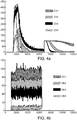
- Fig. 4a shows measured counts over 12000 short measurement periods of 100 ⁇ s on 4 different energy channels Ch1 to Ch4 at four different respective thresholds (30keV, 33keV, 36keV, 51keV).
- the X-ray irradiation starts (a shutter is opened), and at about 7000 measurement periods the X-ray irradiation stops (the shutter is closed). Due to polarization effects in the detecting material volume after the onset of the X-ray irradiation, the number of counts breaks down for later measurement periods. The upcoming space charge weakens the electric field so that fewer electrons reach the anode, which manifests itself in a reduced number of counts. Depending on the actual threshold value this break down is observed at different points in time.
- the WO 2004/095067 A1 discloses an x-ray detector element which can be used in particular in a flat dynamic x-ray detector (FDXD).
- a directly converting conversion layer is arranged between an electrode layer and a matrix of pixel electrodes, there also being a photoconductive separating layer between the pixel electrodes and the conversion layer.
- the separating layer acts as an electrical barrier for free charge carriers of the conversion layer, which have been produced by x-radiation and migrate in the electric field between the electrodes.
- the separating layer can be rendered conductive by illumination with reset light from a diode arrangement, so that charge accumulations at its interface can flow away.
- the US 7 223 981 B1 discloses gamma-ray detector modules with a semiconductor detector array substrate having a plurality of detector cell pads on a first surface thereof, the pads having a contact metallization and a solder barrier metallization.
- An interposer card has planar dimensions no larger than planr dimensions of the semiconductor detector array substrate, a plurality of interconnect pads on a first surface thereof, at least one read-out semiconductor chip and at least one connector on a second surface thereof, each having planar dimensions no larger than the planar dimensions of the interposer card.
- the interposer may house read-out devices, optional passive components, and other support electronics. It provides interconnections for these to the detection elements and to the module motherboard through a connector, such as a pin grid array.
- radiation photons reduce the tendency towards polarization within pixels of the direct conversion material so that counting at higher X-ray fluxes becomes possible.
- the added IR light causes deep traps to be released so that no space charge comes into being.
- the radiation to be detected is not simply absorbed by the direct conversion material and can generate electron-hole pairs (e.g. at defect states). If the proposed IR irradiation is done from the side, where there is not metallization, the IR light is not absorbed (strictly speaking: only absorbed by defect states), so that also pixels which are farthest away from the IR light source still receive sufficient sub-band IR light.
- the plurality of infrared radiation sources are adapted to irradiate the directly converting semiconductor layer with a sub-band infrared radiation having a photon energy smaller than the band gap of the directly converting semiconductor layer. Radiation photons with energies smaller than the band gap further reduce the tendency towards polarization within pixels of the direct conversion material
- the plurality of infrared radiation sources is provided on an infrared source layer which is interposed between the directly converting semiconductor layer and a readout chip of the substrate and which is flip-chip bonded to the directly converting semiconductor layer via the pixel pads. Such a structure with flip-chip bonding allows high packing densities due to the 4-side-buttable structure.
- each of the plurality of infrared radiation sources may be arranged at a gap portion of the pixel pads, i.e., where the direct conversion material is not covered by pad metallization. Thereby, at least a part of the IR radiation can enter the directly converting semiconductor layer without any damping by electrode metallization.
- the infrared source layer comprises through-connection-portions for electrically connecting the pixel pads to related contact portions on the readout chip. This measure reduces wiring complexity and thus further increases packaging density.
- the plurality of infrared sources may comprise a plurality of groups each consisting of infrared sources with different wavelengths of the sub-band infrared radiation.
- efficiency of IR irradiation can be increased by providing a wider radiation spectrum.
- each infrared source of one of the plurality of groups may be arranged at a different corner of a respective pixel pad of the directly converting semiconductor layer. Thereby, spatial distribution of the different wavelengths can be balanced.
- the plurality of infrared sources may be arranged to irradiate the directly converting semiconductor layer from an anode side. This provides the advantage that radiation loss due to electrode metallization can be reduced since the anode electrode is provided with gap portion.
- each of the infrared sources may be allocated to a subset of pixels of the radiation detector. This reduces the number of infrared sources and allows higher packaging densities.
- the directly converting semiconductor layer may be made of a Cd[Zn]Te crystal. This material allows fast photon counting.
- the notation Cd[Zn]Te is used to represent two materials CdTe and CdZnTe (i.e. CZT).
- the manufacturing process comprises interposing the infrared source layer with the plurality of infrared radiation sources between the directly converting semiconductor layer and the readout chip.
- the manufacturing process may comprise bonding the directly converting semiconductor layer to the readout chip with the connected or integrated infrared radiation sources.
- the manufacturing method may further comprise using the infrared source layer as an interposer to test the directly converting semiconductor layer before mounting it to the readout chip.
- the effect of the proposed additional IR radiation can be evaluated during the manufacturing process.
- Fig. 1 shows schematically and exemplarily a cross-sectional side view of a radiation detector according to a first embodiment with an IR LED layer 10 interposed between a 4-side-buttable CMOS (Complementary Metal Oxide Semiconductor) readout circuit or chip 50, e.g. and application specific integrated circuit (ASIC), and a CZT crystal 60.
- CMOS Complementary Metal Oxide Semiconductor
- ASIC application specific integrated circuit
- the CZT crystal 60 is flip-chip bonded via pixel pads 20 to a substrate (i.e. IR LED layer 10 and readout chip 50) which does the readout.
- an IR irradiation device i.e.
- the IR LED layer 10 is integrated into the readout chip 50 to which the CZT crystal 60 is flip-chip bonded, so that a 4-side-buttable crystal is achieved, in which electrical input/output circuits are arranged under the device rather than at its edge.
- This 3-D packaging allows extremely close spacing of radiation detectors.
- Irradiation with sub-band IR LED light where the optical photons have an energy which is smaller than the band gap, reduces the tendency towards polarization within pixels of the CZT crystal 60 so that counting at higher X-ray fluxes becomes possible.
- IR irradiation from the side has the disadvantage that it only allows for 3-side-buttable detector modules. In order to support 4-side-buttable detectors, IR irradiation can be done from the cathode side (i.e. upper side in Fig. 1 ), where the cathode metallization (not shown) probably may not be an obstacle, since it is thin. Then, however, the IR LED layer 10 is within the X-ray beam.
- IR irradiation can be done from the anode side (i.e. lower side in Fig. 1 ), which is advantageous since on the anode side, there are anyway non-metalized regions. The IR irradiation would further be improved, if these pixel gaps are irradiated.
- the pixels of the readout electronics of the readout chip 50 are bonded via respective solder bumps and through connection portions 40 directly to the pixel pads 20 of the CZT crystal 60. Additionally, a supply contact 42 for the IR LED layer 10 is provided.
- the substrate with the readout circuit also implements - besides the readout electronics - one or more sub-band IR LED sources 30.
- more than one IR LED source 30 per pixel may be implemented, if different IR light wavelengths are to be used, which may help to release even more charges of deep traps of different energies.
- the IR LED sources 30 may be implemented on a different substrate (i.e. the IR LED layer 10), which is then flip-chip bonded to the readout electronics of the readout chip 50 manufactured in CMOS technology, as discussed e.g. in McKendry et al.: "Individually addressable AlInGaN micro-LED arrays with CMOS control and subnanosecond output pulses", IEEE Photonics Techn Let, Vol. 21, No. 12, June 15, 2009 .
- the CMOS substrate of the readout chip 50 implements the contact pad for each pixel and may also implement the power supply for the IR LED layer 10.
- the IR LED layer 10 through-contacts the pixel pads 20 by the through connection portions 40 so that the IR LED layer 10 can be flip-chip bonded to the CZT crystal 50, where the emitting dots of the IR LED sources 30 on the IR LED layer 10 illuminate pixel gaps or through the thin pad metallization of the pixel pads 20.
- the LED IR layer 10 can be used as an interposer to also test the CZT crystal 60 before mounting it to the readout electronics, so that after mounting the LED IR layer 10, the CZT crystal 60 can be tested as to its performance for energy-resolved X-ray photon detection together with IR light irradiation.
- the CZT crystal 60 can be tested as to its performance for energy-resolved X-ray photon detection together with IR light irradiation.
- Fig. 2 shows schematically and exemplarily a top view (towards the anode side) of the radiation detector according to the first embodiment with a 2D arrangement of the IR LED sources 30 on the IR LED layer 10 for a single IR wavelength.
- the IR LED sources 30 are arranged at the pixel gaps between the pixel pads 20 of the CZT crystal 60 (not shown in Fig. 2 ).
- Fig. 3 shows schematically and exemplarily a top view (towards the anode side) of a radiation detector according to a second embodiment with a 2D arrangement for IR LED sources 32 providing four different IR wavelengths.
- four IR LED sources 32 of different IR wavelengths are arranged at the edges of neighbouring pixel pads 20 of the CZT crystal 60 (not shown in Fig. 3 ).
- the IR LED sources 30, 32 may be integrated into the CMOS readout chip 50.
- E.g., organic LEDs (OLEDs) may be integrated into a Si CMOS ASIC. With such an integration, further simplifications of the embodiments are possible.
- Fig. 4b shows a diagram similar to Fig. 4a and indicating measured photon counts over the number of short measurement periods of 100 ⁇ s on 4 different energy channels Ch1 to Ch4 with four different thresholds (30keV, 33keV, 36keV, 51keV) with added IR-LED irradiation (880nm).
- the IR light causes the count rate drop to disappear, which can be explained by the deep traps being released so that no space charge comes into being.
- the IR light is not simply absorbed by the CZT material and can generate electron-hole pairs (due to defect states).
- IR irradiation was done from the side. Since the light is not absorbed, also pixels which are farthest away from the light source still receive sufficient sub-band IR light.
- IR irradiation considerably reduces polarization in the directly converting semiconductor material when irradiated, so that counting is possible at higher tube currents without any baseline shift.
- An IR irradiation device is integrated into the readout circuit to which the crystal is flip-chip bonded in order to enable 4-side-buttable crystals.
- the radiation to be detected is X-ray
- the radiation source can be a radiation source generating light within another wavelength range, for instance, in the visible wavelength range.
- the radiation source can also be a lasing device.
- sub-band infra-red light is discussed, also other radiation wavelengths may allow for reducing polarization effects.
- the present invention is not intended to be limited to sub-band radiation.
- the described IR sources may be IR laser diodes instead of the IR LEDs 30, or other radiation sources with other wavelengths.
- the readout chip 50 is not intended to be restricted to CMOS technology and can be implemented based on any other semiconductor technology.
- the direct conversion material is not restricted to CZT.
- any other suitable semiconductor material in the form of CdTe, CdTeSe, CdZnTeSe, CdMnTe, InP, TIBr2 or HGI2 can be used instead of the CZT crystal 60 for detecting X-ray or other radiation photons
- a single unit or device may fulfill the functions of several items recited in the claims.
- the mere fact that certain measures are recited in mutually different dependent claims does not indicate that a combination of these measures cannot be used to advantage.
Landscapes
- Physics & Mathematics (AREA)
- General Physics & Mathematics (AREA)
- Spectroscopy & Molecular Physics (AREA)
- Health & Medical Sciences (AREA)
- Life Sciences & Earth Sciences (AREA)
- High Energy & Nuclear Physics (AREA)
- Molecular Biology (AREA)
- Solid State Image Pick-Up Elements (AREA)
- Measurement Of Radiation (AREA)
- Light Receiving Elements (AREA)
- Transforming Light Signals Into Electric Signals (AREA)
Applications Claiming Priority (2)
| Application Number | Priority Date | Filing Date | Title |
|---|---|---|---|
| US201261724317P | 2012-11-09 | 2012-11-09 | |
| PCT/IB2013/059990 WO2014072939A1 (en) | 2012-11-09 | 2013-11-08 | Sub-band infra-red irradiation for detector crystals |
Publications (2)
| Publication Number | Publication Date |
|---|---|
| EP2917766A1 EP2917766A1 (en) | 2015-09-16 |
| EP2917766B1 true EP2917766B1 (en) | 2019-11-06 |
Family
ID=49713431
Family Applications (1)
| Application Number | Title | Priority Date | Filing Date |
|---|---|---|---|
| EP13799686.4A Active EP2917766B1 (en) | 2012-11-09 | 2013-11-08 | Sub-band infra-red irradiation for detector crystals |
Country Status (7)
Families Citing this family (14)
| Publication number | Priority date | Publication date | Assignee | Title |
|---|---|---|---|---|
| JP6050561B1 (ja) | 2014-09-26 | 2016-12-21 | コーニンクレッカ フィリップス エヌ ヴェKoninklijke Philips N.V. | 加熱装置を有する放射線検出器、それを動作させる方法及びそれを有するイメージング装置 |
| US9571765B2 (en) | 2015-06-25 | 2017-02-14 | General Electric Company | Universal four-side buttable digital CMOS imager |
| EP3320375B1 (en) * | 2015-07-09 | 2019-02-06 | Koninklijke Philips N.V. | Direct conversion radiation detector |
| US10725188B2 (en) | 2015-10-20 | 2020-07-28 | Koninklijke Philips N.V. | Polarization correction for direct conversion x-ray detectors |
| DE102015220793A1 (de) * | 2015-10-23 | 2017-04-27 | Siemens Healthcare Gmbh | Röntgendetektor und/oder Gammadetektor mit Lichtbias |
| US9588240B1 (en) | 2015-10-27 | 2017-03-07 | General Electric Company | Digital readout architecture for four side buttable digital X-ray detector |
| US10686003B2 (en) | 2015-12-31 | 2020-06-16 | General Electric Company | Radiation detector assembly |
| US10283557B2 (en) | 2015-12-31 | 2019-05-07 | General Electric Company | Radiation detector assembly |
| DE102016210935B4 (de) * | 2016-06-20 | 2020-07-09 | Siemens Healthcare Gmbh | Röntgendetektor mit intransparenter Zwischenschicht |
| CN109690355B (zh) * | 2016-09-23 | 2022-10-21 | 深圳帧观德芯科技有限公司 | 具有多层半导体x射线检测器的系统 |
| EP3422051A1 (en) | 2017-06-28 | 2019-01-02 | Koninklijke Philips N.V. | Direct conversion radiation detection |
| WO2020010593A1 (en) * | 2018-07-12 | 2020-01-16 | Shenzhen Xpectvision Technology Co., Ltd. | Methods of making a radiation detector |
| EP3605151A1 (en) * | 2018-08-01 | 2020-02-05 | Koninklijke Philips N.V. | Photon counting detector |
| DE102018219061A1 (de) * | 2018-10-25 | 2020-04-30 | Redlen Technologies, Inc. | Röntgen-zu-infrarot-umwandlungsstrukturen zum beleuchten von röntgendetektoren mit infrarotlicht für verbesserte leistung |
Citations (1)
| Publication number | Priority date | Publication date | Assignee | Title |
|---|---|---|---|---|
| US20030020019A1 (en) * | 2001-07-06 | 2003-01-30 | Hans-Aloys Wischmann | Flat dynamic radiation detector |
Family Cites Families (19)
| Publication number | Priority date | Publication date | Assignee | Title |
|---|---|---|---|---|
| JPS61223689A (ja) * | 1985-03-29 | 1986-10-04 | Shimadzu Corp | 半導体放射線位置検出装置 |
| JP2564979B2 (ja) * | 1990-09-26 | 1996-12-18 | 株式会社島津製作所 | 放射線検出器 |
| US5677539A (en) | 1995-10-13 | 1997-10-14 | Digirad | Semiconductor radiation detector with enhanced charge collection |
| DE19616545B4 (de) | 1996-04-25 | 2006-05-11 | Siemens Ag | Schneller Strahlungsdetektor |
| EP0848885B1 (en) * | 1996-07-08 | 2004-10-06 | Koninklijke Philips Electronics N.V. | X-ray examination apparatus with a semiconductor x-ray detector |
| US6373064B1 (en) * | 1998-10-02 | 2002-04-16 | Sandia Corporation | Semiconductor radiation spectrometer |
| JP4211435B2 (ja) * | 2002-08-30 | 2009-01-21 | 株式会社島津製作所 | 放射線検出器 |
| US7223981B1 (en) * | 2002-12-04 | 2007-05-29 | Aguila Technologies Inc. | Gamma ray detector modules |
| US7379528B2 (en) * | 2003-01-06 | 2008-05-27 | Koninklijke Philips Electronics N.V. | Radiation detector with shielded electronics for computed tomography |
| JP2007527987A (ja) * | 2003-04-24 | 2007-10-04 | コーニンクレッカ フィリップス エレクトロニクス エヌ ヴィ | X線検出器素子 |
| JP2005024368A (ja) * | 2003-07-01 | 2005-01-27 | Fuji Photo Film Co Ltd | 放射線画像検出器の残像消去方法および装置 |
| DE102005037898B3 (de) * | 2005-08-10 | 2007-04-12 | Siemens Ag | Festkörperdetektor bzw. Verfahren zur Rücksetzung von Restladungen durch Beleuchtung bei einem Festkörperdetektor |
| US7652258B2 (en) * | 2007-01-08 | 2010-01-26 | Orbotech Medical Solutions Ltd. | Method, apparatus, and system of reducing polarization in radiation detectors |
| EP2088451B1 (en) * | 2008-02-05 | 2016-01-06 | PANalytical B.V. | Imaging detector |
| US20100078558A1 (en) * | 2008-09-26 | 2010-04-01 | Michael Prokesch | Infra-red light stimulated cdZnTe spectroscopic semiconductor x-ray and gamma-ray radiation detector |
| DE102010015422B4 (de) | 2010-04-19 | 2013-04-18 | Siemens Aktiengesellschaft | Röntgendetektor mit einer direkt konvertierenden Halbleiterschicht und Kalibrierverfahren für einen solchen Röntgendetektor |
| KR101761817B1 (ko) * | 2011-03-04 | 2017-07-26 | 삼성전자주식회사 | 대면적 엑스선 검출기 |
| CN103562746B (zh) * | 2011-05-11 | 2018-08-07 | 皇家飞利浦有限公司 | 电离辐射探测 |
| DE102012213404B3 (de) * | 2012-07-31 | 2014-01-23 | Siemens Aktiengesellschaft | Verfahren zur Temperaturstabilisierung, Röntgenstrahlungsdetektor und CT-System |
-
2013
- 2013-11-08 RU RU2015121968A patent/RU2015121968A/ru not_active Application Discontinuation
- 2013-11-08 EP EP13799686.4A patent/EP2917766B1/en active Active
- 2013-11-08 CN CN201380058602.6A patent/CN104781695B/zh active Active
- 2013-11-08 BR BR112015010277A patent/BR112015010277A2/pt not_active IP Right Cessation
- 2013-11-08 WO PCT/IB2013/059990 patent/WO2014072939A1/en active Application Filing
- 2013-11-08 JP JP2015541280A patent/JP6310471B2/ja active Active
- 2013-11-08 US US14/440,609 patent/US9664558B2/en active Active
Patent Citations (1)
| Publication number | Priority date | Publication date | Assignee | Title |
|---|---|---|---|---|
| US20030020019A1 (en) * | 2001-07-06 | 2003-01-30 | Hans-Aloys Wischmann | Flat dynamic radiation detector |
Also Published As
| Publication number | Publication date |
|---|---|
| RU2015121968A (ru) | 2017-01-10 |
| JP6310471B2 (ja) | 2018-04-11 |
| EP2917766A1 (en) | 2015-09-16 |
| BR112015010277A2 (pt) | 2017-07-11 |
| JP2016504567A (ja) | 2016-02-12 |
| CN104781695B (zh) | 2019-06-28 |
| CN104781695A (zh) | 2015-07-15 |
| WO2014072939A1 (en) | 2014-05-15 |
| US9664558B2 (en) | 2017-05-30 |
| US20150285676A1 (en) | 2015-10-08 |
Similar Documents
| Publication | Publication Date | Title |
|---|---|---|
| EP2917766B1 (en) | Sub-band infra-red irradiation for detector crystals | |
| US7170049B2 (en) | Pixelated cadmium zinc telluride based photon counting mode detector | |
| CN101273898B (zh) | 使用固态光电倍增器和闪烁器的光子计数ct探测器 | |
| US9109953B2 (en) | Photodetector and computed tomography apparatus | |
| RU2445647C2 (ru) | Детектор излучения с несколькими электродами на чувствительном слое | |
| US10007007B2 (en) | Methods for making an X-ray detector | |
| US20080240341A1 (en) | Hybrid energy discriminating charge integrating ct detector | |
| US20140077089A1 (en) | Neutron detector | |
| TWI675219B (zh) | 檢測器 | |
| US20240248218A1 (en) | X-ray detector component, x-ray detection module, imaging device and method for manufacturing an x-ray detector component | |
| US8017902B2 (en) | Detector | |
| CN108369285A (zh) | 半导体x射线检测器的封装方法 | |
| WO2005062073A1 (ja) | 放射線検出器 | |
| Acerbi et al. | High sensitivity photodetector for photon-counting applications | |
| D’Ascenzo et al. | Current status and development of CMOS SiPM for scintillator-based radiation detectors toward all-digital sensors | |
| CN116247066B (zh) | X射线探测器和探测方法 | |
| WO2024044925A1 (en) | Side incidence image sensors with protruding integrated circuit chips | |
| WO2023123302A1 (en) | Imaging methods using bi-directional counters | |
| WO2023015564A1 (en) | Determination of photon origination points using radiation detectors | |
| WO2025046220A1 (en) | Detection device | |
| CN118215861A (zh) | 具有屏蔽电子器件层的图像传感器 | |
| CN118401864A (zh) | 具有成像期间进行侧面辐射入射的图像传感器的成像系统 | |
| US20190086559A1 (en) | Detector array for imaging modality | |
| JP2013050398A (ja) | 放射線二次元検出装置 |
Legal Events
| Date | Code | Title | Description |
|---|---|---|---|
| PUAI | Public reference made under article 153(3) epc to a published international application that has entered the european phase |
Free format text: ORIGINAL CODE: 0009012 |
|
| 17P | Request for examination filed |
Effective date: 20150609 |
|
| AK | Designated contracting states |
Kind code of ref document: A1 Designated state(s): AL AT BE BG CH CY CZ DE DK EE ES FI FR GB GR HR HU IE IS IT LI LT LU LV MC MK MT NL NO PL PT RO RS SE SI SK SM TR |
|
| AX | Request for extension of the european patent |
Extension state: BA ME |
|
| DAX | Request for extension of the european patent (deleted) | ||
| STAA | Information on the status of an ep patent application or granted ep patent |
Free format text: STATUS: EXAMINATION IS IN PROGRESS |
|
| 17Q | First examination report despatched |
Effective date: 20170303 |
|
| GRAP | Despatch of communication of intention to grant a patent |
Free format text: ORIGINAL CODE: EPIDOSNIGR1 |
|
| STAA | Information on the status of an ep patent application or granted ep patent |
Free format text: STATUS: GRANT OF PATENT IS INTENDED |
|
| INTG | Intention to grant announced |
Effective date: 20190528 |
|
| RIN1 | Information on inventor provided before grant (corrected) |
Inventor name: STEADMAN BOOKER, ROGER Inventor name: HERRMANN, CHRISTOPH |
|
| GRAS | Grant fee paid |
Free format text: ORIGINAL CODE: EPIDOSNIGR3 |
|
| GRAA | (expected) grant |
Free format text: ORIGINAL CODE: 0009210 |
|
| STAA | Information on the status of an ep patent application or granted ep patent |
Free format text: STATUS: THE PATENT HAS BEEN GRANTED |
|
| AK | Designated contracting states |
Kind code of ref document: B1 Designated state(s): AL AT BE BG CH CY CZ DE DK EE ES FI FR GB GR HR HU IE IS IT LI LT LU LV MC MK MT NL NO PL PT RO RS SE SI SK SM TR |
|
| REG | Reference to a national code |
Ref country code: GB Ref legal event code: FG4D |
|
| REG | Reference to a national code |
Ref country code: CH Ref legal event code: EP Ref country code: AT Ref legal event code: REF Ref document number: 1199522 Country of ref document: AT Kind code of ref document: T Effective date: 20191115 |
|
| REG | Reference to a national code |
Ref country code: IE Ref legal event code: FG4D |
|
| REG | Reference to a national code |
Ref country code: DE Ref legal event code: R096 Ref document number: 602013062614 Country of ref document: DE |
|
| REG | Reference to a national code |
Ref country code: DE Ref legal event code: R084 Ref document number: 602013062614 Country of ref document: DE |
|
| REG | Reference to a national code |
Ref country code: GB Ref legal event code: 746 Effective date: 20200210 |
|
| REG | Reference to a national code |
Ref country code: NL Ref legal event code: MP Effective date: 20191106 |
|
| RAP2 | Party data changed (patent owner data changed or rights of a patent transferred) |
Owner name: PHILIPS GMBH Owner name: KONINKLIJKE PHILIPS N.V. |
|
| REG | Reference to a national code |
Ref country code: LT Ref legal event code: MG4D |
|
| PG25 | Lapsed in a contracting state [announced via postgrant information from national office to epo] |
Ref country code: FI Free format text: LAPSE BECAUSE OF FAILURE TO SUBMIT A TRANSLATION OF THE DESCRIPTION OR TO PAY THE FEE WITHIN THE PRESCRIBED TIME-LIMIT Effective date: 20191106 Ref country code: BG Free format text: LAPSE BECAUSE OF FAILURE TO SUBMIT A TRANSLATION OF THE DESCRIPTION OR TO PAY THE FEE WITHIN THE PRESCRIBED TIME-LIMIT Effective date: 20200206 Ref country code: LV Free format text: LAPSE BECAUSE OF FAILURE TO SUBMIT A TRANSLATION OF THE DESCRIPTION OR TO PAY THE FEE WITHIN THE PRESCRIBED TIME-LIMIT Effective date: 20191106 Ref country code: SE Free format text: LAPSE BECAUSE OF FAILURE TO SUBMIT A TRANSLATION OF THE DESCRIPTION OR TO PAY THE FEE WITHIN THE PRESCRIBED TIME-LIMIT Effective date: 20191106 Ref country code: NL Free format text: LAPSE BECAUSE OF FAILURE TO SUBMIT A TRANSLATION OF THE DESCRIPTION OR TO PAY THE FEE WITHIN THE PRESCRIBED TIME-LIMIT Effective date: 20191106 Ref country code: LT Free format text: LAPSE BECAUSE OF FAILURE TO SUBMIT A TRANSLATION OF THE DESCRIPTION OR TO PAY THE FEE WITHIN THE PRESCRIBED TIME-LIMIT Effective date: 20191106 Ref country code: PL Free format text: LAPSE BECAUSE OF FAILURE TO SUBMIT A TRANSLATION OF THE DESCRIPTION OR TO PAY THE FEE WITHIN THE PRESCRIBED TIME-LIMIT Effective date: 20191106 Ref country code: PT Free format text: LAPSE BECAUSE OF FAILURE TO SUBMIT A TRANSLATION OF THE DESCRIPTION OR TO PAY THE FEE WITHIN THE PRESCRIBED TIME-LIMIT Effective date: 20200306 Ref country code: NO Free format text: LAPSE BECAUSE OF FAILURE TO SUBMIT A TRANSLATION OF THE DESCRIPTION OR TO PAY THE FEE WITHIN THE PRESCRIBED TIME-LIMIT Effective date: 20200206 Ref country code: GR Free format text: LAPSE BECAUSE OF FAILURE TO SUBMIT A TRANSLATION OF THE DESCRIPTION OR TO PAY THE FEE WITHIN THE PRESCRIBED TIME-LIMIT Effective date: 20200207 |
|
| PG25 | Lapsed in a contracting state [announced via postgrant information from national office to epo] |
Ref country code: IS Free format text: LAPSE BECAUSE OF FAILURE TO SUBMIT A TRANSLATION OF THE DESCRIPTION OR TO PAY THE FEE WITHIN THE PRESCRIBED TIME-LIMIT Effective date: 20200306 Ref country code: HR Free format text: LAPSE BECAUSE OF FAILURE TO SUBMIT A TRANSLATION OF THE DESCRIPTION OR TO PAY THE FEE WITHIN THE PRESCRIBED TIME-LIMIT Effective date: 20191106 Ref country code: RS Free format text: LAPSE BECAUSE OF FAILURE TO SUBMIT A TRANSLATION OF THE DESCRIPTION OR TO PAY THE FEE WITHIN THE PRESCRIBED TIME-LIMIT Effective date: 20191106 |
|
| PG25 | Lapsed in a contracting state [announced via postgrant information from national office to epo] |
Ref country code: AL Free format text: LAPSE BECAUSE OF FAILURE TO SUBMIT A TRANSLATION OF THE DESCRIPTION OR TO PAY THE FEE WITHIN THE PRESCRIBED TIME-LIMIT Effective date: 20191106 |
|
| REG | Reference to a national code |
Ref country code: CH Ref legal event code: PL |
|
| PG25 | Lapsed in a contracting state [announced via postgrant information from national office to epo] |
Ref country code: LI Free format text: LAPSE BECAUSE OF NON-PAYMENT OF DUE FEES Effective date: 20191130 Ref country code: ES Free format text: LAPSE BECAUSE OF FAILURE TO SUBMIT A TRANSLATION OF THE DESCRIPTION OR TO PAY THE FEE WITHIN THE PRESCRIBED TIME-LIMIT Effective date: 20191106 Ref country code: RO Free format text: LAPSE BECAUSE OF FAILURE TO SUBMIT A TRANSLATION OF THE DESCRIPTION OR TO PAY THE FEE WITHIN THE PRESCRIBED TIME-LIMIT Effective date: 20191106 Ref country code: CZ Free format text: LAPSE BECAUSE OF FAILURE TO SUBMIT A TRANSLATION OF THE DESCRIPTION OR TO PAY THE FEE WITHIN THE PRESCRIBED TIME-LIMIT Effective date: 20191106 Ref country code: LU Free format text: LAPSE BECAUSE OF NON-PAYMENT OF DUE FEES Effective date: 20191108 Ref country code: EE Free format text: LAPSE BECAUSE OF FAILURE TO SUBMIT A TRANSLATION OF THE DESCRIPTION OR TO PAY THE FEE WITHIN THE PRESCRIBED TIME-LIMIT Effective date: 20191106 Ref country code: CH Free format text: LAPSE BECAUSE OF NON-PAYMENT OF DUE FEES Effective date: 20191130 Ref country code: DK Free format text: LAPSE BECAUSE OF FAILURE TO SUBMIT A TRANSLATION OF THE DESCRIPTION OR TO PAY THE FEE WITHIN THE PRESCRIBED TIME-LIMIT Effective date: 20191106 |
|
| REG | Reference to a national code |
Ref country code: DE Ref legal event code: R097 Ref document number: 602013062614 Country of ref document: DE |
|
| REG | Reference to a national code |
Ref country code: AT Ref legal event code: MK05 Ref document number: 1199522 Country of ref document: AT Kind code of ref document: T Effective date: 20191106 |
|
| REG | Reference to a national code |
Ref country code: BE Ref legal event code: MM Effective date: 20191130 |
|
| PG25 | Lapsed in a contracting state [announced via postgrant information from national office to epo] |
Ref country code: MC Free format text: LAPSE BECAUSE OF FAILURE TO SUBMIT A TRANSLATION OF THE DESCRIPTION OR TO PAY THE FEE WITHIN THE PRESCRIBED TIME-LIMIT Effective date: 20191106 Ref country code: SK Free format text: LAPSE BECAUSE OF FAILURE TO SUBMIT A TRANSLATION OF THE DESCRIPTION OR TO PAY THE FEE WITHIN THE PRESCRIBED TIME-LIMIT Effective date: 20191106 Ref country code: SM Free format text: LAPSE BECAUSE OF FAILURE TO SUBMIT A TRANSLATION OF THE DESCRIPTION OR TO PAY THE FEE WITHIN THE PRESCRIBED TIME-LIMIT Effective date: 20191106 |
|
| PLBE | No opposition filed within time limit |
Free format text: ORIGINAL CODE: 0009261 |
|
| STAA | Information on the status of an ep patent application or granted ep patent |
Free format text: STATUS: NO OPPOSITION FILED WITHIN TIME LIMIT |
|
| 26N | No opposition filed |
Effective date: 20200807 |
|
| PG25 | Lapsed in a contracting state [announced via postgrant information from national office to epo] |
Ref country code: FR Free format text: LAPSE BECAUSE OF NON-PAYMENT OF DUE FEES Effective date: 20200106 Ref country code: IE Free format text: LAPSE BECAUSE OF NON-PAYMENT OF DUE FEES Effective date: 20191108 |
|
| PG25 | Lapsed in a contracting state [announced via postgrant information from national office to epo] |
Ref country code: AT Free format text: LAPSE BECAUSE OF FAILURE TO SUBMIT A TRANSLATION OF THE DESCRIPTION OR TO PAY THE FEE WITHIN THE PRESCRIBED TIME-LIMIT Effective date: 20191106 Ref country code: BE Free format text: LAPSE BECAUSE OF NON-PAYMENT OF DUE FEES Effective date: 20191130 Ref country code: SI Free format text: LAPSE BECAUSE OF FAILURE TO SUBMIT A TRANSLATION OF THE DESCRIPTION OR TO PAY THE FEE WITHIN THE PRESCRIBED TIME-LIMIT Effective date: 20191106 |
|
| REG | Reference to a national code |
Ref country code: DE Ref legal event code: R081 Ref document number: 602013062614 Country of ref document: DE Owner name: PHILIPS GMBH, DE Free format text: FORMER OWNER: PHILIPS GMBH, 20099 HAMBURG, DE |
|
| PG25 | Lapsed in a contracting state [announced via postgrant information from national office to epo] |
Ref country code: IT Free format text: LAPSE BECAUSE OF FAILURE TO SUBMIT A TRANSLATION OF THE DESCRIPTION OR TO PAY THE FEE WITHIN THE PRESCRIBED TIME-LIMIT Effective date: 20191106 |
|
| PG25 | Lapsed in a contracting state [announced via postgrant information from national office to epo] |
Ref country code: CY Free format text: LAPSE BECAUSE OF FAILURE TO SUBMIT A TRANSLATION OF THE DESCRIPTION OR TO PAY THE FEE WITHIN THE PRESCRIBED TIME-LIMIT Effective date: 20191106 |
|
| PG25 | Lapsed in a contracting state [announced via postgrant information from national office to epo] |
Ref country code: HU Free format text: LAPSE BECAUSE OF FAILURE TO SUBMIT A TRANSLATION OF THE DESCRIPTION OR TO PAY THE FEE WITHIN THE PRESCRIBED TIME-LIMIT; INVALID AB INITIO Effective date: 20131108 Ref country code: MT Free format text: LAPSE BECAUSE OF FAILURE TO SUBMIT A TRANSLATION OF THE DESCRIPTION OR TO PAY THE FEE WITHIN THE PRESCRIBED TIME-LIMIT Effective date: 20191106 |
|
| PG25 | Lapsed in a contracting state [announced via postgrant information from national office to epo] |
Ref country code: TR Free format text: LAPSE BECAUSE OF FAILURE TO SUBMIT A TRANSLATION OF THE DESCRIPTION OR TO PAY THE FEE WITHIN THE PRESCRIBED TIME-LIMIT Effective date: 20191106 |
|
| PG25 | Lapsed in a contracting state [announced via postgrant information from national office to epo] |
Ref country code: MK Free format text: LAPSE BECAUSE OF FAILURE TO SUBMIT A TRANSLATION OF THE DESCRIPTION OR TO PAY THE FEE WITHIN THE PRESCRIBED TIME-LIMIT Effective date: 20191106 |
|
| PGFP | Annual fee paid to national office [announced via postgrant information from national office to epo] |
Ref country code: DE Payment date: 20241128 Year of fee payment: 12 |
|
| PGFP | Annual fee paid to national office [announced via postgrant information from national office to epo] |
Ref country code: GB Payment date: 20241126 Year of fee payment: 12 |