EP2916354A2 - Ultra-thin embedded semiconductor device package and method of manufacturing thereof - Google Patents
Ultra-thin embedded semiconductor device package and method of manufacturing thereof Download PDFInfo
- Publication number
- EP2916354A2 EP2916354A2 EP15157300.3A EP15157300A EP2916354A2 EP 2916354 A2 EP2916354 A2 EP 2916354A2 EP 15157300 A EP15157300 A EP 15157300A EP 2916354 A2 EP2916354 A2 EP 2916354A2
- Authority
- EP
- European Patent Office
- Prior art keywords
- package structure
- semiconductor device
- dielectric layer
- external circuit
- connections
- Prior art date
- Legal status (The legal status is an assumption and is not a legal conclusion. Google has not performed a legal analysis and makes no representation as to the accuracy of the status listed.)
- Ceased
Links
Images




Classifications
-
- H—ELECTRICITY
- H05—ELECTRIC TECHNIQUES NOT OTHERWISE PROVIDED FOR
- H05K—PRINTED CIRCUITS; CASINGS OR CONSTRUCTIONAL DETAILS OF ELECTRIC APPARATUS; MANUFACTURE OF ASSEMBLAGES OF ELECTRICAL COMPONENTS
- H05K3/00—Apparatus or processes for manufacturing printed circuits
- H05K3/30—Assembling printed circuits with electric components, e.g. with resistors
- H05K3/303—Assembling printed circuits with electric components, e.g. with resistors with surface mounted components
- H05K3/305—Affixing by adhesive
-
- H—ELECTRICITY
- H05—ELECTRIC TECHNIQUES NOT OTHERWISE PROVIDED FOR
- H05K—PRINTED CIRCUITS; CASINGS OR CONSTRUCTIONAL DETAILS OF ELECTRIC APPARATUS; MANUFACTURE OF ASSEMBLAGES OF ELECTRICAL COMPONENTS
- H05K1/00—Printed circuits
- H05K1/02—Details
- H05K1/0201—Thermal arrangements, e.g. for cooling, heating or preventing overheating
- H05K1/0203—Cooling of mounted components
- H05K1/0204—Cooling of mounted components using means for thermal conduction connection in the thickness direction of the substrate
- H05K1/0206—Cooling of mounted components using means for thermal conduction connection in the thickness direction of the substrate by printed thermal vias
-
- H—ELECTRICITY
- H05—ELECTRIC TECHNIQUES NOT OTHERWISE PROVIDED FOR
- H05K—PRINTED CIRCUITS; CASINGS OR CONSTRUCTIONAL DETAILS OF ELECTRIC APPARATUS; MANUFACTURE OF ASSEMBLAGES OF ELECTRICAL COMPONENTS
- H05K3/00—Apparatus or processes for manufacturing printed circuits
- H05K3/30—Assembling printed circuits with electric components, e.g. with resistors
- H05K3/301—Assembling printed circuits with electric components, e.g. with resistors by means of a mounting structure
-
- H—ELECTRICITY
- H05—ELECTRIC TECHNIQUES NOT OTHERWISE PROVIDED FOR
- H05K—PRINTED CIRCUITS; CASINGS OR CONSTRUCTIONAL DETAILS OF ELECTRIC APPARATUS; MANUFACTURE OF ASSEMBLAGES OF ELECTRICAL COMPONENTS
- H05K3/00—Apparatus or processes for manufacturing printed circuits
- H05K3/36—Assembling printed circuits with other printed circuits
- H05K3/366—Assembling printed circuits with other printed circuits substantially perpendicularly to each other
-
- H—ELECTRICITY
- H05—ELECTRIC TECHNIQUES NOT OTHERWISE PROVIDED FOR
- H05K—PRINTED CIRCUITS; CASINGS OR CONSTRUCTIONAL DETAILS OF ELECTRIC APPARATUS; MANUFACTURE OF ASSEMBLAGES OF ELECTRICAL COMPONENTS
- H05K3/00—Apparatus or processes for manufacturing printed circuits
- H05K3/46—Manufacturing multilayer circuits
- H05K3/4602—Manufacturing multilayer circuits characterized by a special circuit board as base or central core whereon additional circuit layers are built or additional circuit boards are laminated
-
- H—ELECTRICITY
- H10—SEMICONDUCTOR DEVICES; ELECTRIC SOLID-STATE DEVICES NOT OTHERWISE PROVIDED FOR
- H10W—GENERIC PACKAGES, INTERCONNECTIONS, CONNECTORS OR OTHER CONSTRUCTIONAL DETAILS OF DEVICES COVERED BY CLASS H10
- H10W20/00—Interconnections in chips, wafers or substrates
- H10W20/20—Interconnections within wafers or substrates, e.g. through-silicon vias [TSV]
-
- H—ELECTRICITY
- H10—SEMICONDUCTOR DEVICES; ELECTRIC SOLID-STATE DEVICES NOT OTHERWISE PROVIDED FOR
- H10W—GENERIC PACKAGES, INTERCONNECTIONS, CONNECTORS OR OTHER CONSTRUCTIONAL DETAILS OF DEVICES COVERED BY CLASS H10
- H10W40/00—Arrangements for thermal protection or thermal control
-
- H—ELECTRICITY
- H10—SEMICONDUCTOR DEVICES; ELECTRIC SOLID-STATE DEVICES NOT OTHERWISE PROVIDED FOR
- H10W—GENERIC PACKAGES, INTERCONNECTIONS, CONNECTORS OR OTHER CONSTRUCTIONAL DETAILS OF DEVICES COVERED BY CLASS H10
- H10W40/00—Arrangements for thermal protection or thermal control
- H10W40/20—Arrangements for cooling
- H10W40/22—Arrangements for cooling characterised by their shape, e.g. having conical or cylindrical projections
-
- H—ELECTRICITY
- H10—SEMICONDUCTOR DEVICES; ELECTRIC SOLID-STATE DEVICES NOT OTHERWISE PROVIDED FOR
- H10W—GENERIC PACKAGES, INTERCONNECTIONS, CONNECTORS OR OTHER CONSTRUCTIONAL DETAILS OF DEVICES COVERED BY CLASS H10
- H10W40/00—Arrangements for thermal protection or thermal control
- H10W40/20—Arrangements for cooling
- H10W40/25—Arrangements for cooling characterised by their materials
-
- H—ELECTRICITY
- H10—SEMICONDUCTOR DEVICES; ELECTRIC SOLID-STATE DEVICES NOT OTHERWISE PROVIDED FOR
- H10W—GENERIC PACKAGES, INTERCONNECTIONS, CONNECTORS OR OTHER CONSTRUCTIONAL DETAILS OF DEVICES COVERED BY CLASS H10
- H10W70/00—Package substrates; Interposers; Redistribution layers [RDL]
- H10W70/01—Manufacture or treatment
- H10W70/05—Manufacture or treatment of insulating or insulated package substrates, or of interposers, or of redistribution layers
- H10W70/08—Manufacture or treatment of insulating or insulated package substrates, or of interposers, or of redistribution layers by depositing layers on the chip or wafer, e.g. "chip-first" RDLs
- H10W70/09—Manufacture or treatment of insulating or insulated package substrates, or of interposers, or of redistribution layers by depositing layers on the chip or wafer, e.g. "chip-first" RDLs extending onto an encapsulation that laterally surrounds the chip or wafer, e.g. fan-out wafer level package [FOWLP] RDLs
-
- H—ELECTRICITY
- H10—SEMICONDUCTOR DEVICES; ELECTRIC SOLID-STATE DEVICES NOT OTHERWISE PROVIDED FOR
- H10W—GENERIC PACKAGES, INTERCONNECTIONS, CONNECTORS OR OTHER CONSTRUCTIONAL DETAILS OF DEVICES COVERED BY CLASS H10
- H10W70/00—Package substrates; Interposers; Redistribution layers [RDL]
- H10W70/01—Manufacture or treatment
- H10W70/05—Manufacture or treatment of insulating or insulated package substrates, or of interposers, or of redistribution layers
- H10W70/093—Connecting or disconnecting other interconnections thereto or therefrom, e.g. connecting bond wires or bumps
-
- H—ELECTRICITY
- H10—SEMICONDUCTOR DEVICES; ELECTRIC SOLID-STATE DEVICES NOT OTHERWISE PROVIDED FOR
- H10W—GENERIC PACKAGES, INTERCONNECTIONS, CONNECTORS OR OTHER CONSTRUCTIONAL DETAILS OF DEVICES COVERED BY CLASS H10
- H10W70/00—Package substrates; Interposers; Redistribution layers [RDL]
- H10W70/60—Insulating or insulated package substrates; Interposers; Redistribution layers
- H10W70/611—Insulating or insulated package substrates; Interposers; Redistribution layers for connecting multiple chips together
- H10W70/614—Insulating or insulated package substrates; Interposers; Redistribution layers for connecting multiple chips together the multiple chips being integrally enclosed
-
- H—ELECTRICITY
- H10—SEMICONDUCTOR DEVICES; ELECTRIC SOLID-STATE DEVICES NOT OTHERWISE PROVIDED FOR
- H10W—GENERIC PACKAGES, INTERCONNECTIONS, CONNECTORS OR OTHER CONSTRUCTIONAL DETAILS OF DEVICES COVERED BY CLASS H10
- H10W72/00—Interconnections or connectors in packages
- H10W72/071—Connecting or disconnecting
- H10W72/073—Connecting or disconnecting of die-attach connectors
-
- H—ELECTRICITY
- H10—SEMICONDUCTOR DEVICES; ELECTRIC SOLID-STATE DEVICES NOT OTHERWISE PROVIDED FOR
- H10W—GENERIC PACKAGES, INTERCONNECTIONS, CONNECTORS OR OTHER CONSTRUCTIONAL DETAILS OF DEVICES COVERED BY CLASS H10
- H10W90/00—Package configurations
-
- H—ELECTRICITY
- H05—ELECTRIC TECHNIQUES NOT OTHERWISE PROVIDED FOR
- H05K—PRINTED CIRCUITS; CASINGS OR CONSTRUCTIONAL DETAILS OF ELECTRIC APPARATUS; MANUFACTURE OF ASSEMBLAGES OF ELECTRICAL COMPONENTS
- H05K1/00—Printed circuits
- H05K1/02—Details
- H05K1/0201—Thermal arrangements, e.g. for cooling, heating or preventing overheating
- H05K1/0203—Cooling of mounted components
- H05K1/0209—External configuration of printed circuit board adapted for heat dissipation, e.g. lay-out of conductors, coatings
-
- H—ELECTRICITY
- H05—ELECTRIC TECHNIQUES NOT OTHERWISE PROVIDED FOR
- H05K—PRINTED CIRCUITS; CASINGS OR CONSTRUCTIONAL DETAILS OF ELECTRIC APPARATUS; MANUFACTURE OF ASSEMBLAGES OF ELECTRICAL COMPONENTS
- H05K1/00—Printed circuits
- H05K1/18—Printed circuits structurally associated with non-printed electric components
- H05K1/182—Printed circuits structurally associated with non-printed electric components associated with components mounted in printed circuit boards [PCB], e.g. insert-mounted components [IMC]
- H05K1/183—Printed circuits structurally associated with non-printed electric components associated with components mounted in printed circuit boards [PCB], e.g. insert-mounted components [IMC] associated with components mounted in and supported by recessed areas of the PCBs
-
- H—ELECTRICITY
- H05—ELECTRIC TECHNIQUES NOT OTHERWISE PROVIDED FOR
- H05K—PRINTED CIRCUITS; CASINGS OR CONSTRUCTIONAL DETAILS OF ELECTRIC APPARATUS; MANUFACTURE OF ASSEMBLAGES OF ELECTRICAL COMPONENTS
- H05K1/00—Printed circuits
- H05K1/18—Printed circuits structurally associated with non-printed electric components
- H05K1/182—Printed circuits structurally associated with non-printed electric components associated with components mounted in printed circuit boards [PCB], e.g. insert-mounted components [IMC]
- H05K1/185—Printed circuits structurally associated with non-printed electric components associated with components mounted in printed circuit boards [PCB], e.g. insert-mounted components [IMC] associated with components encapsulated in the insulating substrate of the PCBs; associated with components incorporated in internal layers of multilayer circuit boards
-
- H—ELECTRICITY
- H05—ELECTRIC TECHNIQUES NOT OTHERWISE PROVIDED FOR
- H05K—PRINTED CIRCUITS; CASINGS OR CONSTRUCTIONAL DETAILS OF ELECTRIC APPARATUS; MANUFACTURE OF ASSEMBLAGES OF ELECTRICAL COMPONENTS
- H05K2201/00—Indexing scheme relating to printed circuits covered by H05K1/00
- H05K2201/01—Dielectrics
- H05K2201/0183—Dielectric layers
- H05K2201/0195—Dielectric or adhesive layers comprising a plurality of layers, e.g. in a multilayer structure
-
- H—ELECTRICITY
- H05—ELECTRIC TECHNIQUES NOT OTHERWISE PROVIDED FOR
- H05K—PRINTED CIRCUITS; CASINGS OR CONSTRUCTIONAL DETAILS OF ELECTRIC APPARATUS; MANUFACTURE OF ASSEMBLAGES OF ELECTRICAL COMPONENTS
- H05K2201/00—Indexing scheme relating to printed circuits covered by H05K1/00
- H05K2201/09—Shape and layout
- H05K2201/09818—Shape or layout details not covered by a single group of H05K2201/09009 - H05K2201/09809
- H05K2201/09845—Stepped hole, via, edge, bump or conductor
-
- H—ELECTRICITY
- H05—ELECTRIC TECHNIQUES NOT OTHERWISE PROVIDED FOR
- H05K—PRINTED CIRCUITS; CASINGS OR CONSTRUCTIONAL DETAILS OF ELECTRIC APPARATUS; MANUFACTURE OF ASSEMBLAGES OF ELECTRICAL COMPONENTS
- H05K2203/00—Indexing scheme relating to apparatus or processes for manufacturing printed circuits covered by H05K3/00
- H05K2203/30—Details of processes not otherwise provided for in H05K2203/01 - H05K2203/17
- H05K2203/302—Bending a rigid substrate; Breaking rigid substrates by bending
-
- H—ELECTRICITY
- H05—ELECTRIC TECHNIQUES NOT OTHERWISE PROVIDED FOR
- H05K—PRINTED CIRCUITS; CASINGS OR CONSTRUCTIONAL DETAILS OF ELECTRIC APPARATUS; MANUFACTURE OF ASSEMBLAGES OF ELECTRICAL COMPONENTS
- H05K3/00—Apparatus or processes for manufacturing printed circuits
- H05K3/30—Assembling printed circuits with electric components, e.g. with resistors
- H05K3/306—Assembling printed circuits with electric components, e.g. with resistors with lead-in-hole components
-
- H—ELECTRICITY
- H10—SEMICONDUCTOR DEVICES; ELECTRIC SOLID-STATE DEVICES NOT OTHERWISE PROVIDED FOR
- H10W—GENERIC PACKAGES, INTERCONNECTIONS, CONNECTORS OR OTHER CONSTRUCTIONAL DETAILS OF DEVICES COVERED BY CLASS H10
- H10W40/00—Arrangements for thermal protection or thermal control
- H10W40/70—Fillings or auxiliary members in containers or in encapsulations for thermal protection or control
-
- H—ELECTRICITY
- H10—SEMICONDUCTOR DEVICES; ELECTRIC SOLID-STATE DEVICES NOT OTHERWISE PROVIDED FOR
- H10W—GENERIC PACKAGES, INTERCONNECTIONS, CONNECTORS OR OTHER CONSTRUCTIONAL DETAILS OF DEVICES COVERED BY CLASS H10
- H10W40/00—Arrangements for thermal protection or thermal control
- H10W40/70—Fillings or auxiliary members in containers or in encapsulations for thermal protection or control
- H10W40/77—Auxiliary members characterised by their shape
-
- H—ELECTRICITY
- H10—SEMICONDUCTOR DEVICES; ELECTRIC SOLID-STATE DEVICES NOT OTHERWISE PROVIDED FOR
- H10W—GENERIC PACKAGES, INTERCONNECTIONS, CONNECTORS OR OTHER CONSTRUCTIONAL DETAILS OF DEVICES COVERED BY CLASS H10
- H10W70/00—Package substrates; Interposers; Redistribution layers [RDL]
- H10W70/60—Insulating or insulated package substrates; Interposers; Redistribution layers
-
- H—ELECTRICITY
- H10—SEMICONDUCTOR DEVICES; ELECTRIC SOLID-STATE DEVICES NOT OTHERWISE PROVIDED FOR
- H10W—GENERIC PACKAGES, INTERCONNECTIONS, CONNECTORS OR OTHER CONSTRUCTIONAL DETAILS OF DEVICES COVERED BY CLASS H10
- H10W72/00—Interconnections or connectors in packages
- H10W72/01—Manufacture or treatment
- H10W72/013—Manufacture or treatment of die-attach connectors
- H10W72/01351—Changing the shapes of die-attach connectors
-
- H—ELECTRICITY
- H10—SEMICONDUCTOR DEVICES; ELECTRIC SOLID-STATE DEVICES NOT OTHERWISE PROVIDED FOR
- H10W—GENERIC PACKAGES, INTERCONNECTIONS, CONNECTORS OR OTHER CONSTRUCTIONAL DETAILS OF DEVICES COVERED BY CLASS H10
- H10W72/00—Interconnections or connectors in packages
- H10W72/01—Manufacture or treatment
- H10W72/015—Manufacture or treatment of bond wires
-
- H—ELECTRICITY
- H10—SEMICONDUCTOR DEVICES; ELECTRIC SOLID-STATE DEVICES NOT OTHERWISE PROVIDED FOR
- H10W—GENERIC PACKAGES, INTERCONNECTIONS, CONNECTORS OR OTHER CONSTRUCTIONAL DETAILS OF DEVICES COVERED BY CLASS H10
- H10W72/00—Interconnections or connectors in packages
- H10W72/071—Connecting or disconnecting
- H10W72/073—Connecting or disconnecting of die-attach connectors
- H10W72/07351—Connecting or disconnecting of die-attach connectors characterised by changes in properties of the die-attach connectors during connecting
- H10W72/07355—Connecting or disconnecting of die-attach connectors characterised by changes in properties of the die-attach connectors during connecting changes in materials
-
- H—ELECTRICITY
- H10—SEMICONDUCTOR DEVICES; ELECTRIC SOLID-STATE DEVICES NOT OTHERWISE PROVIDED FOR
- H10W—GENERIC PACKAGES, INTERCONNECTIONS, CONNECTORS OR OTHER CONSTRUCTIONAL DETAILS OF DEVICES COVERED BY CLASS H10
- H10W72/00—Interconnections or connectors in packages
- H10W72/071—Connecting or disconnecting
- H10W72/075—Connecting or disconnecting of bond wires
-
- H—ELECTRICITY
- H10—SEMICONDUCTOR DEVICES; ELECTRIC SOLID-STATE DEVICES NOT OTHERWISE PROVIDED FOR
- H10W—GENERIC PACKAGES, INTERCONNECTIONS, CONNECTORS OR OTHER CONSTRUCTIONAL DETAILS OF DEVICES COVERED BY CLASS H10
- H10W72/00—Interconnections or connectors in packages
- H10W72/30—Die-attach connectors
- H10W72/351—Materials of die-attach connectors
-
- H—ELECTRICITY
- H10—SEMICONDUCTOR DEVICES; ELECTRIC SOLID-STATE DEVICES NOT OTHERWISE PROVIDED FOR
- H10W—GENERIC PACKAGES, INTERCONNECTIONS, CONNECTORS OR OTHER CONSTRUCTIONAL DETAILS OF DEVICES COVERED BY CLASS H10
- H10W72/00—Interconnections or connectors in packages
- H10W72/30—Die-attach connectors
- H10W72/351—Materials of die-attach connectors
- H10W72/353—Materials of die-attach connectors not comprising solid metals or solid metalloids, e.g. ceramics
- H10W72/354—Materials of die-attach connectors not comprising solid metals or solid metalloids, e.g. ceramics comprising polymers
-
- H—ELECTRICITY
- H10—SEMICONDUCTOR DEVICES; ELECTRIC SOLID-STATE DEVICES NOT OTHERWISE PROVIDED FOR
- H10W—GENERIC PACKAGES, INTERCONNECTIONS, CONNECTORS OR OTHER CONSTRUCTIONAL DETAILS OF DEVICES COVERED BY CLASS H10
- H10W72/00—Interconnections or connectors in packages
- H10W72/50—Bond wires
-
- H—ELECTRICITY
- H10—SEMICONDUCTOR DEVICES; ELECTRIC SOLID-STATE DEVICES NOT OTHERWISE PROVIDED FOR
- H10W—GENERIC PACKAGES, INTERCONNECTIONS, CONNECTORS OR OTHER CONSTRUCTIONAL DETAILS OF DEVICES COVERED BY CLASS H10
- H10W72/00—Interconnections or connectors in packages
- H10W72/50—Bond wires
- H10W72/551—Materials of bond wires
- H10W72/552—Materials of bond wires comprising metals or metalloids, e.g. silver
- H10W72/5525—Materials of bond wires comprising metals or metalloids, e.g. silver comprising copper [Cu]
-
- H—ELECTRICITY
- H10—SEMICONDUCTOR DEVICES; ELECTRIC SOLID-STATE DEVICES NOT OTHERWISE PROVIDED FOR
- H10W—GENERIC PACKAGES, INTERCONNECTIONS, CONNECTORS OR OTHER CONSTRUCTIONAL DETAILS OF DEVICES COVERED BY CLASS H10
- H10W72/00—Interconnections or connectors in packages
- H10W72/90—Bond pads, in general
- H10W72/931—Shapes of bond pads
-
- H—ELECTRICITY
- H10—SEMICONDUCTOR DEVICES; ELECTRIC SOLID-STATE DEVICES NOT OTHERWISE PROVIDED FOR
- H10W—GENERIC PACKAGES, INTERCONNECTIONS, CONNECTORS OR OTHER CONSTRUCTIONAL DETAILS OF DEVICES COVERED BY CLASS H10
- H10W72/00—Interconnections or connectors in packages
- H10W72/90—Bond pads, in general
- H10W72/941—Dispositions of bond pads
- H10W72/9413—Dispositions of bond pads on encapsulations
-
- H—ELECTRICITY
- H10—SEMICONDUCTOR DEVICES; ELECTRIC SOLID-STATE DEVICES NOT OTHERWISE PROVIDED FOR
- H10W—GENERIC PACKAGES, INTERCONNECTIONS, CONNECTORS OR OTHER CONSTRUCTIONAL DETAILS OF DEVICES COVERED BY CLASS H10
- H10W72/00—Interconnections or connectors in packages
- H10W72/90—Bond pads, in general
- H10W72/951—Materials of bond pads
-
- H—ELECTRICITY
- H10—SEMICONDUCTOR DEVICES; ELECTRIC SOLID-STATE DEVICES NOT OTHERWISE PROVIDED FOR
- H10W—GENERIC PACKAGES, INTERCONNECTIONS, CONNECTORS OR OTHER CONSTRUCTIONAL DETAILS OF DEVICES COVERED BY CLASS H10
- H10W90/00—Package configurations
- H10W90/10—Configurations of laterally-adjacent chips
-
- H—ELECTRICITY
- H10—SEMICONDUCTOR DEVICES; ELECTRIC SOLID-STATE DEVICES NOT OTHERWISE PROVIDED FOR
- H10W—GENERIC PACKAGES, INTERCONNECTIONS, CONNECTORS OR OTHER CONSTRUCTIONAL DETAILS OF DEVICES COVERED BY CLASS H10
- H10W90/00—Package configurations
- H10W90/20—Configurations of stacked chips
- H10W90/288—Configurations of stacked chips characterised by arrangements for thermal management of the stacked chips
-
- H—ELECTRICITY
- H10—SEMICONDUCTOR DEVICES; ELECTRIC SOLID-STATE DEVICES NOT OTHERWISE PROVIDED FOR
- H10W—GENERIC PACKAGES, INTERCONNECTIONS, CONNECTORS OR OTHER CONSTRUCTIONAL DETAILS OF DEVICES COVERED BY CLASS H10
- H10W90/00—Package configurations
- H10W90/701—Package configurations characterised by the relative positions of pads or connectors relative to package parts
- H10W90/731—Package configurations characterised by the relative positions of pads or connectors relative to package parts of die-attach connectors
- H10W90/734—Package configurations characterised by the relative positions of pads or connectors relative to package parts of die-attach connectors between a chip and a stacked insulating package substrate, interposer or RDL
-
- H—ELECTRICITY
- H10—SEMICONDUCTOR DEVICES; ELECTRIC SOLID-STATE DEVICES NOT OTHERWISE PROVIDED FOR
- H10W—GENERIC PACKAGES, INTERCONNECTIONS, CONNECTORS OR OTHER CONSTRUCTIONAL DETAILS OF DEVICES COVERED BY CLASS H10
- H10W90/00—Package configurations
- H10W90/701—Package configurations characterised by the relative positions of pads or connectors relative to package parts
- H10W90/751—Package configurations characterised by the relative positions of pads or connectors relative to package parts of bond wires
- H10W90/752—Package configurations characterised by the relative positions of pads or connectors relative to package parts of bond wires between stacked chips
-
- Y—GENERAL TAGGING OF NEW TECHNOLOGICAL DEVELOPMENTS; GENERAL TAGGING OF CROSS-SECTIONAL TECHNOLOGIES SPANNING OVER SEVERAL SECTIONS OF THE IPC; TECHNICAL SUBJECTS COVERED BY FORMER USPC CROSS-REFERENCE ART COLLECTIONS [XRACs] AND DIGESTS
- Y02—TECHNOLOGIES OR APPLICATIONS FOR MITIGATION OR ADAPTATION AGAINST CLIMATE CHANGE
- Y02P—CLIMATE CHANGE MITIGATION TECHNOLOGIES IN THE PRODUCTION OR PROCESSING OF GOODS
- Y02P70/00—Climate change mitigation technologies in the production process for final industrial or consumer products
- Y02P70/50—Manufacturing or production processes characterised by the final manufactured product
Definitions
- the I/O connections establish full electrical functionality at the system-level, such that additional/separate leads, terminals or a lead-frame is not needed in the POL package structure 10, resulting in an ultra-thin, miniaturized electrical package with greatly improved electrical and mechanical performance.
- Such elimination of the wire bonds and multi-layer substrate in packaging a power device in the package structure 10 also enables a package structure 10 having a very small form-factor with high device density and a small foot-print, so as to enable system miniaturization to improve electrical and reliability performance of the package.
- the I/O connections of the package structure allow the package structure to be partially embedded in an external circuit, with embodiments of the invention providing for mounting of the package structure in a connector or recess of the PCB either on-edge/vertical relative to the PCB (so as to reduce a board footprint of the package structure) or flat within a recess of the PCB (to reduce an overall height of the PCB assembly).
- a package structure includes a first dielectric layer, at least one semiconductor device attached to the first dielectric layer, and an embedding material applied to the first dielectric layer so as to embed the at least one semiconductor device therein, the embedding material comprising one or more additional dielectric layers.
- the package structure also includes a plurality of vias formed in the first dielectric layer formed to the at least one semiconductor device, metal interconnects formed in the plurality of vias and on one or more outward facing surface of the package structure to form electrical interconnections to the at least one semiconductor device, and input/output (I/O) connections located on one end of the package structure on one or more outward facing surfaces thereof to provide a second level connection to an external circuit.
- the package structure is configured to interfit with a connector formed on the external circuit to mount the package perpendicular to the external circuit, with the I/O connections on the one end of the package structure being electrically connected to the connector to form the second level connection to the external circuit.
Landscapes
- Engineering & Computer Science (AREA)
- Microelectronics & Electronic Packaging (AREA)
- Manufacturing & Machinery (AREA)
- Cooling Or The Like Of Semiconductors Or Solid State Devices (AREA)
- Production Of Multi-Layered Print Wiring Board (AREA)
- Combinations Of Printed Boards (AREA)
- Structures Or Materials For Encapsulating Or Coating Semiconductor Devices Or Solid State Devices (AREA)
Abstract
Description
- Embodiments of the invention relate generally to structures and methods for packaging semiconductor devices and, more particularly, to an ultra-thin power device packaging structure having power overlay (POL) interconnects that form all electrical and thermal interconnections in the structure, with the packaging structure having reduced inductance.
- Power semiconductor devices are semiconductor devices used as switches or rectifiers in power electronic circuits, such as switched mode power supplies, for example. In use, power semiconductor devices are typically surface mounted to an external circuit by way of a packaging structure, with the packaging structure providing an electrical connection to the external circuit and also providing a way to remove the heat generated by the devices and protect the devices from the external environment. Alternatively, especially for higher power ranges, the power modules packaging structures may have large terminals for connection to the external circuit which add significant inductance and increase the size of the module.
- Most existing power device packaging structures use wirebonds, a multi-layer substrate (e.g., a direct bond copper (DBC) substrate), and are leaded (leadframe, etc.) or provided with bolted terminals for providing electrical and thermal connectivity to the packaging structure. The wirebonds make the connections from one surface of the packaging structure to package pins, which then interface to the external circuit, with a DBC being connected to the other surface of the packaging structure (e.g., soldered thereto). It is recognized, however, that the DBC adds significant cost to the packaging structure both from a materials standpoint and from a processing standpoint - as additional processing steps and temperature excursions are required when including a DBC in the packaging structure, such as soldering and flux cleaning processes required for joining the DBC to the packaging structure. It is also recognized that the wirebonds and leads add significant parasitic inductance that reduces the efficiency of the package. Wirebonds also add significant height to the package. It is still further recognized that - while the leads on the packaging structure allow higher thermal cycling reliability and are not subject to stringent Moisture Sensitivity Level (MSL) Requirements - the leads or terminals in a power module can be quite large and affect the module foot-print and thickness on the PCB and also negatively impact the electrical performance due to high inductance.
- Therefore, it would be desirable to provide a semiconductor device package structure that eliminates the need for a multi-layer DBC or PCB substrate and wirebond connections, so as to provide a very thin package structure with ultra low inductance. It would further be desirable for such a package structure to have a high device density and a small foot-print, so as to enable system miniaturization to improve electrical and reliability performance of the package.
- In accordance with one aspect of the invention, a package structure includes a first dielectric layer, at least one semiconductor device attached to the first dielectric layer, and an embedding material applied to the first dielectric layer so as to embed the at least one semiconductor device therein, the embedding material comprising one or more additional dielectric layers. The package structure also includes a plurality of vias formed in the first dielectric layer formed to the at least one semiconductor device, metal interconnects formed in the plurality of vias and on one or more outward facing surface of the package structure to form electrical interconnections to the at least one semiconductor device, and input/output (I/O) connections located on one end of the package structure on one or more outward facing surfaces thereof to provide a second level connection to an external circuit. The package structure is configured to interfit with a connector formed on the external circuit to mount the package perpendicular to the external circuit, with the I/O connections on the one end of the package structure being electrically connected to the connector to form the second level connection to the external circuit.
- In accordance with another aspect of the invention, a method of manufacturing a semiconductor device package structure includes attaching at least one semiconductor device to a first dielectric layer by way of an adhesive, applying an embedding material on the first dielectric layer so as to be positioned about the at least one semiconductor device, and performing a lamination process to cause the embedding material to fill any air gaps present around the at least one semiconductor device and so as to embed the at least one semiconductor device therein, wherein the first dielectric layer does not melt or flow during the lamination process. The method also includes forming a plurality of vias to the at least one semiconductor device, forming metallic interconnects in the plurality of vias and over at least a portion of one or more outer surfaces of the package structure to form electrical interconnections to the at least one semiconductor device, and forming input/output (I/O) connections on one or more of the outward facing surfaces of the package structure, at only one end of the package structure, the I/O connections comprising electrical leads that provide a second level connection to an external circuit.
- In accordance with yet another aspect of the invention, a package structure includes a first dielectric layer having an adhesive applied on at least a portion thereof, one or more semiconductor devices attached to the first dielectric layer by way of the adhesive, an embedding material positioned on the first dielectric layer about the one or more semiconductor devices so as to embed the one or more semiconductor devices therein, a plurality of vias formed to the at least one semiconductor device, metal interconnects formed in the plurality of vias to form all electrical and thermal interconnections to the one or more semiconductor devices and in the package structure and input/output (I/O) connections formed on at least one outer surface of the package structure to provide a second level connection to an external circuit, wherein the I/O connections are configured to interfit with a socket or recess formed in the external circuit, such that the package structure is partially embedded in the external circuit when the I/O connections of the package structure are interfit in socket or recess.
- These and other advantages and features will be more readily understood from the following detailed description of preferred embodiments of the invention that is provided in connection with the accompanying drawings.
- The drawings illustrate embodiments presently contemplated for carrying out the invention.
- In the drawings:
-
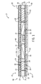
FIG. 1 is a schematic cross-sectional side view of a power overlay (POL) package structure, according to an embodiment of the invention. -
FIG. 2 is a schematic cross-sectional side view of a POL package structure, according to an embodiment of the invention. -
FIG. 3 is a schematic cross-sectional side view of a POL package structure, according to an embodiment of the invention. -
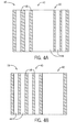
FIGS. 4A and 4B are front and back views of input/output (I/O) connections formed on one end of the POL package structures ofFIGS. 1 and2 . -
FIGS. 5A and 5B are front and side views of the POL package structures ofFIGS. 1 and2 inserted/embedded into a connector of a printed circuit board (PCB), according to an embodiment of the invention. -
FIG. 6 is a side view of a POL package structure inserted/embedded into a connector of a printed circuit board (PCB), according to an embodiment of the invention. -
FIG. 7 is a side view of the POL package structures ofFIGS. 1 and2 inserted/embedded into a connector of a printed circuit board, with heat sinks affixed to the package structure and PCB, according to an embodiment of the invention. -
FIG. 8 is a schematic cross-sectional side view of a POL package structure mounted on/embedded in a PCB, according to an embodiment of the invention. -
FIG. 9 is a schematic cross-sectional side view of a POL package structure mounted on/embedded in a PCB, according to an embodiment of the invention. - Embodiments of the present invention provide for an embedded power module package structure having power overlay (POL) interconnects that form all electrical and thermal interconnections to the semiconductor devices in the power module, as well as a method of forming such a package structure. The package structure is constructed to have an "ultra-thin" construction in two axes, and may be partially embedded in an external circuit (e.g., PCB) to which the package structure is mounted.
- Referring to
FIG. 1 , a POL packaging andinterconnect structure 10 is shown according to an embodiment of the invention. Thepackage structure 10 includes one ormore semiconductor devices power semiconductor devices 12 and a single non-power semiconductor device 13 (i.e., gate driver) are shown inFIG. 1 , it is recognized that a lesser or greater number of semiconductor devices or electronic components could be included in thePOL structure 10. Thesemiconductor devices package structure 10 such that direct metallic interconnects form all electrical and/or thermal interconnections to the device. - As shown in
FIG. 1 , according to an exemplary embodiment, thepackage structure 10 includes a dielectric layer on each of opposing sides of the package structure 10 (with thesemiconductor devices dielectric layer 14 and a seconddielectric layer 16. Whilepackage structure 10 includes both firstdielectric layer 14 and a seconddielectric layer 16, it is recognized that embodiments of the invention may only include a firstdielectric layer 14. InFIG. 1 , thedielectric layers dielectric layers dielectric layers package structure 10. That is,dielectric layers package structure 10. Accordingly, thedielectric layers dielectric layers package structure 10, thedielectric layers polyimide layers layers - As shown in
FIG. 1 ,polyimide layers package structure 10, i.e., on front andback surfaces semiconductor devices polyimide layers devices polyimide layers package structure 10 that is provided between thepolyimide layers package structure 10 that might be present around thesemiconductor devices polyimide layers polyimide layer 14 to thedevices - According to one embodiment of the invention, and as shown in
FIG. 1 , theembedding material 24 is comprised of one or moredielectric layers 26 that are provided in a 'film' or 'panel' or 'sheet' form, such that, if required, multipledielectric sheets 26 can be stacked on one another to a required height/thickness required to fill in an area about thesemiconductor devices polyimide layers dielectric sheets 26 are formed from an electrically insulating material, such as a prepreg material, printed circuit board core material, polymeric resin, or other suitable adhesive, for example. According to one embodiment, the electrically insulatingdielectric sheets 26 may be provided in a form that is either uncured or partially cured (i.e., B-stage), such that they can be easily stacked in their pre-cure film form. According to another embodiment, the electrically insulatingdielectric sheets 26 may be provided as both cured and uncured sheets, such as sheets of a cured core material and sheets of a flowable prepreg material or a mixture of sheets of polyimide and a flowable adhesive (e.g., layer 22). Other insulating materials may also be used such as ceramics or glass. According to one embodiment of the invention, the dielectric sheet(s) 26 include openings/cut-outs 28 formed therein to receive thesemiconductor devices dielectric sheets 26 could be placed about thesemiconductor devices - While embedding
material 24 is described above as being comprised of one or moredielectric layers 26 that are provided in a 'film' or 'panel' or 'sheet' form, it is recognized that embeddingmaterial 24 could include other materials. For example, the dielectric stack that is the embeddingmaterial 24 can be comprised of a layer of metal or a dielectric film with thick copper, for example, that does not melt and flow when subjected to a lamination process. In such embodiments, these layers would be electrically isolated as needed from thedevices - In order to fill-up empty gaps within the
package structure 10, the dielectric sheet(s) 26 are subjected to a lamination/curing process (typically in vacuum environment, at elevated temperature and under mechanical pressure) that causes all or some of the dielectric sheet(s) 26 to "melt" and flow. The dielectric sheet(s) 26 thus lose their film form and flow to fill up any empty air gaps around thesemiconductor devices polyimide layers dielectric encapsulant 24 is provided that protects thesemiconductor devices - Referring now to
FIG. 2 , an alternate embodiment ofpackage structure 10 is shown in which the embeddingmaterial 24 is formed only of adhesive 22. That is, in cases where thesemiconductor devices dielectric layers 26 may be required to encapsulate the semiconductor devices. Instead, the adhesive 22 is coated on the surface of thepolyimide layer 14, beyond the area in which thesemiconductor devices semiconductor devices FIG. 2 as being parallel to one another, it is recognized that such an arrangement of the polyimide layers 14, 16 is not required, as the gap between the twopolyimide layers - In each of the embodiments of
package structure 10 shown inFIGS. 1 and2 , a plurality ofvias 30 is formed throughpolyimide layer 14 down to afront surface 32 of thesemiconductor devices power semiconductor devices 12, vias 30 may all be formed tofront surface 32 of the semiconductor devices 12 (e.g., as for GaN power devices) or may instead be formed to both the front surface and back surface 34 of thesemiconductor devices 12, to meet electrical and thermal requirements (e.g., to make electrical connection that is needed and remove heat from the power semiconductor device). Metal interconnects 38 are subsequently formed in thepackage structure 10 to provide electrical and thermal connections/pathways therein, with theinterconnects 38 being formed in thevias 30 and out onto the outward facing front and back surfaces 18, 20 of the polyimide layers 14, 16, respectively, such that both front and back surfaces 18, 20 of thepackage structure 10 include interconnects formed thereon. According to embodiments of the invention, the metal interconnects 38 comprise "POL interconnects" that are formed as robust electroplated copper interconnects that form direct electrical connections in thedevices FIGS. 1 and2 , the metal interconnects 38 are patterned and etched to a desired shape, such as to provide for electrical and thermal connections to packagestructure 10. According to one embodiment, metal interconnects 38 are patterned and etched to provide a large area thermal and electrical connection on the front and/or back side of package structure 10 (i.e., copper pad) that enables attachment of the package structure to a heatsink, for example, as will be explained in greater detail further below. - While the
package structures 10 ofFIGS. 1 and2 are shown as only includingdielectric layers metal interconnects 38 formed therein, it is recognized that a further build-up of the package could be performed. That is, as shown inFIG. 3 , one or more additional metal circuit layers 39 (i.e., dielectric layer and patterned metal interconnect) could be applied to each of the front and back surfaces 18, 20 of the package structure to increase routing in thepackage structure 10. - According to another embodiment, rather than adding additional metal circuit layers to the package structure 10 (as in
FIG. 3 ), routing could be increased in the package structure by adding a metal layer (not shown) on the inward side ofdielectric layers 14, 16 (i.e., on the side of thedevices 12, 13). In such an embodiment, metal layers would thus be present on both sides of eachdielectric layer - Referring now to
FIGS. 1-3 , according to embodiments of the invention, electrical input/output connections (I/Os) 40 are provided onpackaging structure 10 that serve as "electrical leads" that electrically connect thepackage structure 10 to an external circuit, such as a printed circuit board (PCB) - i.e., the I/O connections 40 are utilized to form a second-level interconnection to an external circuit. The I/O connections 40 may be formed as copper pads or traces of plated copper, for example, that are formed on the front and/or back surfaces 18, 20 of the package structure. The I/O connections establish full electrical functionality at the system-level, such that additional/separate leads, terminals or a lead-frame is not needed in thePOL package structure 10, resulting in an ultra-thin, miniaturized electrical package with greatly improved electrical and mechanical performance. - According to an exemplary embodiment of the invention, the I/
O connections 40 that provide the second-level interconnection to the PCB are all located on oneend 42 of the package structure on one or both of the front and back surfaces 18, 20. Detailed views of theend 42 at which the I/O connections 40 are formed are shown inFIGS. 4A and 4B , which illustrate the front and back surfaces 18, 20 of thepackage structure 10 at theend 42. As shown inFIGS. 4A and 4B , the copper pads and/or traces of plated copper forming leads 44 (ondielectric layer 14, 16) of the I/O connections 40 are formed at theend 42 of thepackage structure 10. According to one embodiment, and as best seen inFIGS. 1 and2 , asoldermask 46 may be applied over a remainder of the front and/or back surfaces 18, 20 - i.e., over the patterned POL interconnects 38 - to provide a protective coating for the copper thereof, while leaving the I/O connections 40 on theend 42 uncovered. Additionally, it is recognized that a solder finish or other metal finish (not shown) may be applied on the exposed areas of patterned POL interconnects 38 (left exposed by the solder mask) or the entire surface of the patterned POL interconnects 38. - By providing the I/
O connections 40 of thepackage structure 10 all onend 42, thepackage structure 10 is constructed to be connected to a PCB on-edge. Such an arrangement of thepackage structure 10 with aPCB 48 is shown via front and side views inFIGS. 5A and 5B , with theend 42 of thepackage structure 10 being inserted into a connector orsocket 50 on thePCB 48 such that the I/O connections 40 form a direct electrical connection with theconnector 50. The mounting ofpackage structure 10 on-edge in an upright orientation (i.e., perpendicular) relative to thePCB 48 minimizes the footprint of thepackage structure 10 and thus saves board area, although it does serve to increase the height of the PCB assembly. However, according to one embodiment of the invention, the height of thepackage structure 10 can be reduced by bending the package structure after insertion intosocket 50, as shown inFIG. 6 . Upon bending, a portion/majority of thepackage structure 10 is parallel to thePCB 48, with one embodiment being constructed such that the portion of the package structure including the dies/semiconductor devices is parallel to the PCB. - Referring now to
FIG. 7 , according to one embodiment of the invention, one ormore heat sinks 52 are coupled to thepackage structure 10 on the front and/or back surfaces 18, 20 to assist in heat removal and facilitate thermal management of the package structure. WhileFIG. 7 shows twoheat sinks 52 being affixed to packagestructure 10, it is recognized that only asingle heat sink 52 may be attached to the package structure, such as to backside 20 thereof. The heat sinks 52 may be coupled to thepackage structure 10 such as by adding thermal interface material(s) (TIM) 54 to the backside 20 (and/or front side 18) of the structure. That is, a layer ofTIM 54 having a thermal conductivity is applied onto thePOL structure 10 and over the POL interconnects 38 (and soldermask 46) to provide bonding and the thermal transfer of energy to the heat sinks 52. Examples of suitable TIMs include, without limitation, adhesives, greases, gels, pads, films, liquid metals, compressible metals, and phase change materials. Liquid metal TIMs, for example, are typically indium-gallium alloys that are in liquid state over temperatures typically encountered in power electronics applications. Compressible metals are sufficiently soft to make intimate contact between a heatsink and POL mating surfaces and may include, for example, indium. - In addition to the heat sinks 52 enhancing heat removal from the
package structure 10, the heat sinks 52 also provide mechanical support to the package structure in its on-edge mounting to thePCB 48. That is, in addition to being affixed to package structure 10 (via TIM 54), the heat sinks 52 are also coupled to thePCB 48 such that they provide bracing for thepackage structure 10. Depending on whether one or twoheat sinks 52 are attached to thepackage structure 10, the heat sinks 52 may thus provide additional structural support to thepackage structure 10 on either one or both sides thereof to help maintain thepackage structure 10 in its upright orientation relative to thePCB 48. - Referring now to
FIGS. 8 and 9 ,package structures package structures FIGS. 8 and 9 have a similar construction to thepackage structures 10 illustrated inFIGS. 1 and2 in regards to the embedding of semiconductor devices in an embedding material between dielectric layers and the use of POL interconnects, and thus components in thepackage structures FIGS. 8 and 9 identical to corresponding components in thepackage structure 10 ofFIGS. 1 and2 are similarly numbered. - As shown in
FIGS. 8 and 9 , each of thepackage structures semiconductor devices first dielectric layer 14 and a second dielectric layer 16 (i.e., polyimide layers), with thedevices semiconductor devices dielectric sheets 26 being caused to melt and flow when subjected to a lamination/curing process, such that the dielectric sheet(s) 26 thus lose their film form and flow to fill up any empty air gaps around thesemiconductor devices - In the
package structures 60, 62 a plurality ofvias 30 is formed throughpolyimide layer 14 down to afront surface 32 of thesemiconductor devices power semiconductor devices 12, vias 30 are also formed to backsurface 34 of thesemiconductor devices 12 to meet electrical and thermal requirements. Metal interconnects 38 are subsequently formed in thepackage structure 10 to provide electrical and thermal connections/pathways therein, with theinterconnects 38 being formed in thevias 30 and out onto the outward facing front and back surfaces 18, 20 of the polyimide layers 14, 16, respectively, such that both front and back surfaces 18, 20 of thepackage structure 10 include interconnects formed thereon. According to embodiments of the invention, the metal interconnects 38 comprise "POL interconnects" that are formed as robust electroplated copper interconnects that form direct electrical connections in thedevices structure 10. - Referring to
FIG. 8 , electrical input/output connections (I/Os) 64 are provided onpackaging structure 10 at each of generally opposing ends 66 of the structure that serve as "electrical leads" that electrically connect thepackage structure 10 to anexternal circuit 48, such as a printed circuit board (PCB). According to an embodiment, and as shown inFIG. 8 , I/O connections 64 are formed on thefront surface 18 of thepackage structure 10. Thru-vias 68 are thus be formed through polyimide layers 14, 16 and dielectric sheet(s) 26 that are metalized (i.e., metal interconnects 38 are formed in/through thru-vias 68) to redistribute electrical connections from theback surface 20 to thefront surface 18. While I/O connections 64 are shown as being formed on only thefront surface 18 of thepackage structure 10, it is recognized that the I/O connections 64 could instead be formed on both surfaces of the package - i.e., on front and back surfaces 18, 20 - with the thru-vias 68 not being present in such an embodiment. - As shown in
FIG. 8 , the I/O connections 64 formed on thefront surface 18 of thepackage structure 10 includes leads 70 - with theleads 70 being formed as copper pads or traces of plated copper, for example, that are oriented generally parallel to thesurface 18 of the package structure and that are utilized to form a second-level interconnection to thePCB 48. Asoldermask 46 may be applied over a remainder of the front surface 18 - i.e., over the patterned POL interconnects 38 - to provide a protective coating for the copper thereof, while leaving theleads 70 of I/O connections 64 on thefront surface 18 uncovered. Additionally, it is recognized that a solder finish or other metal finish (not shown) may be applied on the exposed areas of patterned POL interconnects 38 (left exposed by the solder mask) or the entire surface of the patterned POL interconnects 38.As shown inFIG. 8 , thepackage structure 60 is arranged in a "flat" or parallel orientation relative to thePCB 48 and is partially embedded intoPCB 48 via positioning of the package structure into arecess 52 of thePCB 48, withsolder 72 being applied at the location of theleads 70, so as to establish full electrical functionality at the system-level. In this manner, additional/separate leads, terminals or a lead-frame is not needed in thePOL package structure 10, resulting in an ultra-thin, miniaturized electrical package with greatly improved electrical and mechanical performance. As thepackage structure 60 is partially embedded intoPCB 48, a height of the PCB assembly is reduced as compared to an assembly where the package structure is mounted to a generally planar PCB without a recess for receiving a package structure. - Referring now to
FIG. 9 , thepackage structure 62 includes I/O connections 64 formed on thefront surface 18 of thepackage structure 10 that includes leads 74 that extend out perpendicularly from front surface 18 - so as to provide a connectorized construction for thepackage structure 62. That is, rather than theleads 74 of the I/O connections 64 on thefront surface 18 being structured as flat copper pads/traces as in the embodiment ofFIG. 8 , theleads 74 of I/O connections 64 are formed as copper wires or traces (alone or include polyimide material, i.e., polyimide 14) that are bent so as to extend perpendicularly outward fromfront surface 18 of thepackage structure 62. As shown inFIG. 9 , the bent leads 74 of the I/O connections 64 are configured to be inserted/embedded within slots or asocket 76 formed in/on thePCB 48. The leads 74 could then be secured in the slots/socket 76 via sintering, soldering or a mechanical connection (e.g., press-fit), so as to establish full electrical functionality at the system (i.e., a second-level interconnection to the PCB). - Beneficially, embodiments of the invention thus provide a package structure having an "ultra-thin" construction in two axes, with the construction enabling the package structure to be partially embedded in an external circuit (e.g., PCB) to which the package structure is mounted. The use of POL interconnects and I/O connections in the
package structure 10 eliminate the need for wire bonds and/or an additional multi-layer substrate (like a DBC substrate, etc.) that would typically be used for electrical and thermal functionality, thereby providing a package with ultra low inductance by providing a small inductance loop and flux cancellation and the elimination of wirebonds and/or larger leads/terminals that can increase inductance. Such elimination of the wire bonds and multi-layer substrate in packaging a power device in thepackage structure 10 also enables apackage structure 10 having a very small form-factor with high device density and a small foot-print, so as to enable system miniaturization to improve electrical and reliability performance of the package. The I/O connections of the package structure allow the package structure to be partially embedded in an external circuit, with embodiments of the invention providing for mounting of the package structure in a connector or recess of the PCB either on-edge/vertical relative to the PCB (so as to reduce a board footprint of the package structure) or flat within a recess of the PCB (to reduce an overall height of the PCB assembly). - Therefore, according to one embodiment of the invention, a package structure includes a first dielectric layer, at least one semiconductor device attached to the first dielectric layer, and an embedding material applied to the first dielectric layer so as to embed the at least one semiconductor device therein, the embedding material comprising one or more additional dielectric layers. The package structure also includes a plurality of vias formed in the first dielectric layer formed to the at least one semiconductor device, metal interconnects formed in the plurality of vias and on one or more outward facing surface of the package structure to form electrical interconnections to the at least one semiconductor device, and input/output (I/O) connections located on one end of the package structure on one or more outward facing surfaces thereof to provide a second level connection to an external circuit. The package structure is configured to interfit with a connector formed on the external circuit to mount the package perpendicular to the external circuit, with the I/O connections on the one end of the package structure being electrically connected to the connector to form the second level connection to the external circuit.
- According to another embodiment of the invention, a method of manufacturing a semiconductor device package structure includes attaching at least one semiconductor device to a first dielectric layer by way of an adhesive, applying an embedding material on the first dielectric layer so as to be positioned about the at least one semiconductor device, and performing a lamination process to cause the embedding material to fill any air gaps present around the at least one semiconductor device and so as to embed the at least one semiconductor device therein, wherein the first dielectric layer does not melt or flow during the lamination process. The method also includes forming a plurality of vias to the at least one semiconductor device, forming metallic interconnects in the plurality of vias and over at least a portion of one or more outer surfaces of the package structure to form electrical interconnections to the at least one semiconductor device, and forming input/output (I/O) connections on one or more of the outward facing surfaces of the package structure, at only one end of the package structure, the I/O connections comprising electrical leads that provide a second level connection to an external circuit.
- According to yet another embodiment of the invention, a package structure includes a first dielectric layer having an adhesive applied on at least a portion thereof, one or more semiconductor devices attached to the first dielectric layer by way of the adhesive, an embedding material positioned on the first dielectric layer about the one or more semiconductor devices so as to embed the one or more semiconductor devices therein, a plurality of vias formed to the at least one semiconductor device, metal interconnects formed in the plurality of vias to form all electrical and thermal interconnections to the one or more semiconductor devices and in the package structure and input/output (I/O) connections formed on at least one outer surface of the package structure to provide a second level connection to an external circuit, wherein the I/O connections are configured to interfit with a socket or recess formed in the external circuit, such that the package structure is partially embedded in the external circuit when the I/O connections of the package structure are interfit in socket or recess.
- While the invention has been described in detail in connection with only a limited number of embodiments, it should be readily understood that the invention is not limited to such disclosed embodiments. Rather, the invention can be modified to incorporate any number of variations, alterations, substitutions or equivalent arrangements not heretofore described, but which are commensurate with the spirit and scope of the invention. Additionally, while various embodiments of the invention have been described, it is to be understood that aspects of the invention may include only some of the described embodiments. Accordingly, the invention is not to be seen as limited by the foregoing description, but is only limited by the scope of the appended claims.
- Various aspects and embodiments of the present invention are defined by the following numbered clauses:
- 1. A package structure comprising:
- a first dielectric layer;
- at least one semiconductor device attached to the first dielectric layer;
- an embedding material applied to the first dielectric layer so as to embed the at least one semiconductor device therein, the embedding material comprising one or more additional dielectric layers;
- a plurality of vias formed to the at least one semiconductor device, the the plurality of vias formed through the first dielectric layer;
- metal interconnects formed in the plurality of vias and on one or more outward facing surface of the package structure to form electrical interconnections to the at least one semiconductor device; and
- input/output (I/O) connections located on one end of the package structure on one or more outward facing surfaces thereof to provide a second level connection to an external circuit;
- wherein the package structure is configured to interfit with a connector formed on the external circuit to mount the package structure perpendicular to the external circuit, with the I/O connections on the one end of the package structure being electrically connected to the connector to form the second level connection to the external circuit.
- 2. The package structure of clause 1, wherein the I/O connections comprise electrical leads configured to form the second level connection to the external circuit.
- 3. The package structure of clause 1 or 2, wherein the metal interconnects comprise plated copper power overlay (POL) interconnects forming electrical connections on the one or more outward facing surfaces of the package structure, and wherein a portion of the POL interconnects form the electrical leads that form the I/O connections.
- 4. The package structure of any preceding clause, wherein the metal interconnects comprise plated copper power overlay (POL) interconnects forming a heat spreading copper pad on one or more of the outward facing surfaces of the package structure, so as to provide thermal interconnections to the at least one semiconductor device.
- 5. The package structure of clause 4, further comprising:
- a thermal interface material (TIM) applied to the heat spreading copper pad; and
- a heat sink mounted to the TIM to conduct heat away from the package structure.
- 6. The package structure of clause 5, wherein the heat sink is further coupled to the external circuit so as to provide support when mounting the package structure perpendicular to the external circuit.
- 7. The package structure of any preceding clause, wherein the I/O connections are formed on both of the outward facing surfaces of the package structure, on the one end of the package structure.
- 8. The package structure of any preceding clause, further comprising a second dielectric layer positioned on an outward facing surface of the package structure opposite the first dielectric layer, with the at least one semiconductor device and the embedding material being positioned between the first dielectric layer and the second dielectric layer.
- 9. The package structure of clause 8, further comprising an adhesive layer applied on an inward facing surface of at least one of the first and second dielectric layers to secure the at least one semiconductor device thereto, wherein the plurality of vias extend through the adhesive layer.
- 10. The package structure of clause 8 or clause 9, wherein the at least one semiconductor device comprises a power semiconductor device; and
wherein the plurality of vias comprises:- vias formed through the first dielectric layer and the adhesive layer to a front surface of the power semiconductor device; and
- vias formed through the one or more second dielectric layer and the adhesive layer to a back surface of the power semiconductor device;
- wherein the vias function as thermal and electrical vias in the package structure; and
- wherein metal interconnects are formed in each of the vias to the front and back surfaces of the power semiconductor device.
- 11. The package structure of clause 9, further comprising a metal layer positioned on an inward facing surface of the first dielectric layer or the second dielectric layer to increase routing in the package structure.
- 12. The package structure of any preceding clause, wherein the connector of the external circuit comprises an external circuit socket into which the package structure is inserted to mechanically and electrically couple the I/O connections to the external circuit.
- 13. The package structure of any preceding clause, further comprising a solder mask formed over the metal interconnects on the outward facing surfaces of the package structure, with the solder mask not being formed over the I/O connections.
- 14. The package structure of any preceding clause, wherein the mounting of the package structure perpendicular to the external circuit reduces a footprint of the package structure on the external circuit as compared to mounting thereof in a flat orientation.
- 15. The package structure of any preceding clause, wherein the one or more additional dielectric layers of the embedding material comprise one or more dielectric sheets configured to melt and flow when subjected to a lamination process to fill-in any air gaps present around the at least one semiconductor device.
- 16. The package structure of clause 15, wherein the embedding material further comprises a metal layer or a dielectric sheet with copper thermally connected to the plurality of vias to spread and conduct heat to an ambient environment, with the metal layer or dielectric sheet with copper constructed to not melt and flow when subjected to the lamination process.
- 17. The package structure of any preceding clause, further comprising at least one additional metal circuit layer positioned on the outward facing surfaces of the package structure, the at least one additional metal circuit layer being configured to increase routing in the package structure.
- 18. A method of manufacturing a semiconductor device package structure comprising:
- attaching at least one semiconductor device to a first dielectric layer by way of an adhesive;
- applying an embedding material on the first dielectric layer so as to be positioned about the at least one semiconductor device;
- performing a lamination process to cause the embedding material to fill any air gaps present around the at least one semiconductor device and so as to embed the at least one semiconductor device therein, wherein the first dielectric layer does not melt or flow during the lamination process;
- forming a plurality of vias to the at least one semiconductor device;
- forming metallic interconnects in the plurality of vias and over at least a portion of one or more outer surfaces of the package structure, the metallic interconnects forming electrical interconnections to the at least one semiconductor device; and forming input/output (I/O) connections on one or more of the outward facing surfaces of the package structure, at only one end of the package structure, the I/O connections comprising electrical leads that provide a second level connection to an external circuit.
- 19. The method of
clause 18, further comprising mounting the package structure within a corresponding socket or recess of the external circuit at the I/O connections, with the package structure being mounted in the socket or recess on-edge so as to be positioned in an upright orientation relative to the external circuit. - 20. The method of
clause 18 or clause 19, further comprising bending the package structure upon mounting of the package structure within the socket or recess of the external circuit such that a height of the package structure is reduced. - 21. The method of any of
clause 18 to 20, further comprising:- applying a thermal interface material (TIM) over a portion of the metallic interconnects on one or more of the outward facing surfaces of the package structure;
- affixing a heat sink to the TIM on the one or more of the outward facing surfaces of the package structure to conduct heat away from the package structure; and
- coupling the heat sink on the one or more of the outward facing surfaces of the package structure to the external circuit so as to provide support when mounting the package structure in the socket or recess on-edge.
- 22. The method of any of
clauses 18 to 21, further comprising positioning a second dielectric layer over the one or more dielectric sheets such that the at least one semiconductor device and the embedding material are positioned between the first and second dielectric layers, with a portion of the plurality of vias being formed through the second dielectric layer. - 23. The method of any of
clause 18 to 22, wherein applying the embedding material comprises:- forming one or more dielectric sheets; and
- applying the one or more dielectric sheets on the first dielectric layer so as to be positioned about the at least one semiconductor device;
- wherein the one or more dielectric sheets melt and flow during the lamination process to fill any air gaps present around the at least one semiconductor device so as to embed the at least one semiconductor device therein.
- 24. A package structure comprising:
- a first dielectric layer having an adhesive applied on at least a portion thereof;
- one or more semiconductor devices attached to the first dielectric layer by way of the adhesive;
- an embedding material positioned on the first dielectric layer about the one or more semiconductor devices so as to embed the one or more semiconductor devices therein;
- a plurality of vias formed to the at least one semiconductor device;
- metal interconnects formed in the plurality of vias to form all electrical and thermal interconnections to the one or more semiconductor devices and in the package structure; and
- input/output (I/O) connections formed on at least one outer surface of the package structure to provide a second level connection to an external circuit;
- wherein the I/O connections are configured to interfit with a socket or recess formed in the external circuit, such that the package structure is partially embedded in the external circuit when the I/O connections of the package structure are interfit in socket or recess.
- 25. The package structure of
clause 24, wherein the I/O connections are formed at each of opposing edges of the package structure and configured to form the second level connection to the external circuit, the I/O connections comprising one of:- electrical leads formed to be generally parallel to an orientation of the package structure; and
- electrical leads formed to be perpendicular to an orientation of the package structure, with the electrical leads being bent to extend outwardly from the package structure; and
- 26. The package structure of
clause 24 or 25, wherein the I/O connections are formed on one end of the package structure on at least one outer surface thereof to form the second level connection to the external circuit, with the I/O connections on the one end interfitting with the socket or recess formed in the external circuit to mount the package perpendicular to the external circuit.
Claims (15)
- A package structure (10) comprising:a first dielectric layer (14);at least one semiconductor device (12,13) attached to the first dielectric layer;an embedding material (24) applied to the first dielectric layer (14) so as to embed the at least one semiconductor device (12,13) therein, the embedding material (24) comprising one or more additional dielectric layers (26);a plurality of vias (30) formed to the at least one semiconductor device (12,13), the plurality of vias (30) formed through the first dielectric layer (14);metal interconnects (38) formed in the plurality of vias (30) and on one or more outward facing surface (18,20) of the package structure (10) to form electrical interconnections to the at least one semiconductor device (12,13) andinput/output (I/O) connections (40,64) located on one end of the package structure (10) on one or more outward facing surfaces (18,20) thereof to provide a second level connection to an external circuit (48);wherein the package structure (10) s configured to interfit with a connector (50) formed on the external circuit (48) to mount the package structure (10) perpendicular to the external circuit (48), with the I/O connections (40) on the one end of the package structure (10) being electrically connected to the connector (50) to form the second level connection to the external circuit (48).
- The package structure of claim 1, wherein the metal interconnects (38) comprise plated copper power overlay (POL) interconnects forming electrical connections on the one or more outward facing surfaces (18,20) of the package structure (10), and wherein a portion of the POL interconnects form electrical leads (70,74) that form the I/O connections (40,64).
- The package structure of claim 1 or 2, wherein the metal interconnects (38) comprise plated copper power overlay (POL) interconnects forming a heat spreading copper pad on one or more of the outward facing surfaces (18,20) of the package structure (10), so as to provide thermal interconnections to the at least one semiconductor device (12,13).
- The package structure of claim 3, further comprising:a thermal interface material (TIM) applied to the heat spreading copper pad (38); anda heat sink (52) mounted to the TIM (54) to conduct heat away from the package structure (10), wherein the heat sink (52) is further coupled to the external circuit (48) so as to provide support when mounting the package structure (10) perpendicular to the external circuit (48).
- The package structure of any preceding claim, wherein the I/O connections (38) are formed on both of the outward facing surfaces (18,20) of the package structure (10), on the one end of the package structure (10).
- The package structure of any preceding claim, further comprising a second dielectric layer (16) positioned on an outward facing surface of the package structure opposite the first dielectric layer (14), with the at least one semiconductor device (12,13) and the embedding material (24) being positioned between the first dielectric layer (14) and the second dielectric layer (16).
- The package structure of claim 6, further comprising an adhesive layer (22) applied on an inward facing surface of at least one of the first and second dielectric layers (14,16) to secure the at least one semiconductor device (12,13) thereto, wherein the plurality of vias extend through the adhesive layer (22)
- The package structure of claim 7, wherein the at least one semiconductor device (12,13) comprises a power semiconductor device; and
wherein the plurality of vias (30) comprises:vias formed through the first dielectric layer (14) and the adhesive layer (22) to a front surface (32) of the power semiconductor device (12,13); andvias formed through the one or more second dielectric layer (16) and the adhesive layer (22) to a back surface (34) of the power semiconductor device (12,13);wherein the vias (20) function as thermal and electrical vias in the package structure (10); andwherein metal interconnects (38) are formed in each of the vias (30) to the front and back surfaces (32,34) of the power semiconductor device (12,13). - The package structure of claim 8, further comprising a metal layer positioned on an inward facing surface of the first dielectric layer (14) or the second dielectric layer (16) to increase routing in the package structure (10).
- The package structure of any preceding claim, wherein the connector (50) of the external circuit (48) comprises an external circuit socket (76) into which the package structure (10) is inserted to mechanically and electrically couple the I/O connections (38) to the external circuit (48).
- The package structure of any preceding claim, further comprising a solder mask (46) formed over the metal interconnects (38) on the outward facing surfaces (18,20) of the package structure (10), with the solder mask (46) not being formed over the I/O connections (38).
- The package structure of any preceding claim, wherein the one or more additional dielectric layers of the embedding material (24) comprise one or more dielectric sheets (26) configured to melt and flow when subjected to a lamination process to fill-in any air gaps present around the at least one semiconductor device (12,13).
- A method of manufacturing a semiconductor device package structure (10) comprising:attaching at least one semiconductor device (12,13) to a first dielectric layer (14) by way of an adhesive (22);applying an embedding material (24) on the first dielectric layer (14) so as to be positioned about the at least one semiconductor device (12,13);performing a lamination process to cause the embedding material (24) to fill any air gaps present around the at least one semiconductor device (12,13) and so as to embed the at least one semiconductor device (12,13) therein, wherein the first dielectric layer (14) does not melt or flow during the lamination process;forming a plurality of vias (30) to the at least one semiconductor device (12,13);forming metallic interconnects (38) in the plurality of vias (30) and over at least a portion of one or more outer surfaces (18,20) of the package structure (10), the metallic interconnects (38) forming electrical interconnections to the at least one semiconductor device (12,13); andforming input/output (I/O) connections (40) on one or more of the outward facing surfaces (18,20) of the package structure (10), at only one end of the package structure, the I/O connections (40) comprising electrical leads that provide a second level connection to an external circuit (48).
- The method of claim 13, further comprising mounting the package structure (10) within a corresponding socket (70) or recess of the external circuit (48) at the I/O connections (40), with the package structure (10) being mounted in the socket (70) or recess on-edge so as to be positioned in an upright orientation relative to the external circuit (48).
- The method of claim 14, further comprising bending the package structure upon mounting of the package structure within the socket or recess of the external circuit such that a height of the package structure is reduced.
Applications Claiming Priority (1)
| Application Number | Priority Date | Filing Date | Title |
|---|---|---|---|
| US14/195,930 US9806051B2 (en) | 2014-03-04 | 2014-03-04 | Ultra-thin embedded semiconductor device package and method of manufacturing thereof |
Publications (2)
| Publication Number | Publication Date |
|---|---|
| EP2916354A2 true EP2916354A2 (en) | 2015-09-09 |
| EP2916354A3 EP2916354A3 (en) | 2016-06-22 |
Family
ID=52595211
Family Applications (1)
| Application Number | Title | Priority Date | Filing Date |
|---|---|---|---|
| EP15157300.3A Ceased EP2916354A3 (en) | 2014-03-04 | 2015-03-03 | Ultra-thin embedded semiconductor device package and method of manufacturing thereof |
Country Status (5)
| Country | Link |
|---|---|
| US (3) | US9806051B2 (en) |
| EP (1) | EP2916354A3 (en) |
| JP (1) | JP6496571B2 (en) |
| KR (1) | KR102332362B1 (en) |
| CN (1) | CN104900606B (en) |
Cited By (3)
| Publication number | Priority date | Publication date | Assignee | Title |
|---|---|---|---|---|
| EP3270443A1 (en) * | 2016-07-13 | 2018-01-17 | General Electric Company | Embedded dry film battery module and method of manufacturing thereof |
| WO2018017246A1 (en) * | 2016-07-21 | 2018-01-25 | Qualcomm Incorporated | Glass substrate including passive-on-glass device and semiconductor die |
| EP3982404A1 (en) * | 2020-10-07 | 2022-04-13 | Infineon Technologies Austria AG | Semiconductor module |
Families Citing this family (198)
| Publication number | Priority date | Publication date | Assignee | Title |
|---|---|---|---|---|
| US11984445B2 (en) | 2009-10-12 | 2024-05-14 | Monolithic 3D Inc. | 3D semiconductor devices and structures with metal layers |
| US10157909B2 (en) | 2009-10-12 | 2018-12-18 | Monolithic 3D Inc. | 3D semiconductor device and structure |
| US11374118B2 (en) | 2009-10-12 | 2022-06-28 | Monolithic 3D Inc. | Method to form a 3D integrated circuit |
| US10910364B2 (en) | 2009-10-12 | 2021-02-02 | Monolitaic 3D Inc. | 3D semiconductor device |
| US10043781B2 (en) | 2009-10-12 | 2018-08-07 | Monolithic 3D Inc. | 3D semiconductor device and structure |
| US12027518B1 (en) | 2009-10-12 | 2024-07-02 | Monolithic 3D Inc. | 3D semiconductor devices and structures with metal layers |
| US11018133B2 (en) | 2009-10-12 | 2021-05-25 | Monolithic 3D Inc. | 3D integrated circuit |
| US10354995B2 (en) | 2009-10-12 | 2019-07-16 | Monolithic 3D Inc. | Semiconductor memory device and structure |
| US10366970B2 (en) | 2009-10-12 | 2019-07-30 | Monolithic 3D Inc. | 3D semiconductor device and structure |
| US10388863B2 (en) | 2009-10-12 | 2019-08-20 | Monolithic 3D Inc. | 3D memory device and structure |
| US10217667B2 (en) | 2011-06-28 | 2019-02-26 | Monolithic 3D Inc. | 3D semiconductor device, fabrication method and system |
| US10497713B2 (en) | 2010-11-18 | 2019-12-03 | Monolithic 3D Inc. | 3D semiconductor memory device and structure |
| US11482440B2 (en) | 2010-12-16 | 2022-10-25 | Monolithic 3D Inc. | 3D semiconductor device and structure with a built-in test circuit for repairing faulty circuits |
| US12362219B2 (en) | 2010-11-18 | 2025-07-15 | Monolithic 3D Inc. | 3D semiconductor memory device and structure |
| US11227897B2 (en) | 2010-10-11 | 2022-01-18 | Monolithic 3D Inc. | Method for producing a 3D semiconductor memory device and structure |
| US11315980B1 (en) | 2010-10-11 | 2022-04-26 | Monolithic 3D Inc. | 3D semiconductor device and structure with transistors |
| US11024673B1 (en) | 2010-10-11 | 2021-06-01 | Monolithic 3D Inc. | 3D semiconductor device and structure |
| US11158674B2 (en) | 2010-10-11 | 2021-10-26 | Monolithic 3D Inc. | Method to produce a 3D semiconductor device and structure |
| US11600667B1 (en) | 2010-10-11 | 2023-03-07 | Monolithic 3D Inc. | Method to produce 3D semiconductor devices and structures with memory |
| US10290682B2 (en) | 2010-10-11 | 2019-05-14 | Monolithic 3D Inc. | 3D IC semiconductor device and structure with stacked memory |
| US11018191B1 (en) | 2010-10-11 | 2021-05-25 | Monolithic 3D Inc. | 3D semiconductor device and structure |
| US10896931B1 (en) | 2010-10-11 | 2021-01-19 | Monolithic 3D Inc. | 3D semiconductor device and structure |
| US11257867B1 (en) | 2010-10-11 | 2022-02-22 | Monolithic 3D Inc. | 3D semiconductor device and structure with oxide bonds |
| US11469271B2 (en) | 2010-10-11 | 2022-10-11 | Monolithic 3D Inc. | Method to produce 3D semiconductor devices and structures with memory |
| US11437368B2 (en) | 2010-10-13 | 2022-09-06 | Monolithic 3D Inc. | Multilevel semiconductor device and structure with oxide bonding |
| US11133344B2 (en) | 2010-10-13 | 2021-09-28 | Monolithic 3D Inc. | Multilevel semiconductor device and structure with image sensors |
| US11929372B2 (en) | 2010-10-13 | 2024-03-12 | Monolithic 3D Inc. | Multilevel semiconductor device and structure with image sensors and wafer bonding |
| US11694922B2 (en) | 2010-10-13 | 2023-07-04 | Monolithic 3D Inc. | Multilevel semiconductor device and structure with oxide bonding |
| US11327227B2 (en) | 2010-10-13 | 2022-05-10 | Monolithic 3D Inc. | Multilevel semiconductor device and structure with electromagnetic modulators |
| US11164898B2 (en) | 2010-10-13 | 2021-11-02 | Monolithic 3D Inc. | Multilevel semiconductor device and structure |
| US11043523B1 (en) | 2010-10-13 | 2021-06-22 | Monolithic 3D Inc. | Multilevel semiconductor device and structure with image sensors |
| US10978501B1 (en) | 2010-10-13 | 2021-04-13 | Monolithic 3D Inc. | Multilevel semiconductor device and structure with waveguides |
| US12094892B2 (en) | 2010-10-13 | 2024-09-17 | Monolithic 3D Inc. | 3D micro display device and structure |
| US10943934B2 (en) | 2010-10-13 | 2021-03-09 | Monolithic 3D Inc. | Multilevel semiconductor device and structure |
| US11869915B2 (en) | 2010-10-13 | 2024-01-09 | Monolithic 3D Inc. | Multilevel semiconductor device and structure with image sensors and wafer bonding |
| US11855114B2 (en) | 2010-10-13 | 2023-12-26 | Monolithic 3D Inc. | Multilevel semiconductor device and structure with image sensors and wafer bonding |
| US11404466B2 (en) | 2010-10-13 | 2022-08-02 | Monolithic 3D Inc. | Multilevel semiconductor device and structure with image sensors |
| US10679977B2 (en) | 2010-10-13 | 2020-06-09 | Monolithic 3D Inc. | 3D microdisplay device and structure |
| US10998374B1 (en) | 2010-10-13 | 2021-05-04 | Monolithic 3D Inc. | Multilevel semiconductor device and structure |
| US11163112B2 (en) | 2010-10-13 | 2021-11-02 | Monolithic 3D Inc. | Multilevel semiconductor device and structure with electromagnetic modulators |
| US10833108B2 (en) | 2010-10-13 | 2020-11-10 | Monolithic 3D Inc. | 3D microdisplay device and structure |
| US11984438B2 (en) | 2010-10-13 | 2024-05-14 | Monolithic 3D Inc. | Multilevel semiconductor device and structure with oxide bonding |
| US11063071B1 (en) | 2010-10-13 | 2021-07-13 | Monolithic 3D Inc. | Multilevel semiconductor device and structure with waveguides |
| US12080743B2 (en) | 2010-10-13 | 2024-09-03 | Monolithic 3D Inc. | Multilevel semiconductor device and structure with image sensors and wafer bonding |
| US11605663B2 (en) | 2010-10-13 | 2023-03-14 | Monolithic 3D Inc. | Multilevel semiconductor device and structure with image sensors and wafer bonding |
| US12360310B2 (en) | 2010-10-13 | 2025-07-15 | Monolithic 3D Inc. | Multilevel semiconductor device and structure with oxide bonding |
| US11855100B2 (en) | 2010-10-13 | 2023-12-26 | Monolithic 3D Inc. | Multilevel semiconductor device and structure with oxide bonding |
| US11443971B2 (en) | 2010-11-18 | 2022-09-13 | Monolithic 3D Inc. | 3D semiconductor device and structure with memory |
| US12243765B2 (en) | 2010-11-18 | 2025-03-04 | Monolithic 3D Inc. | 3D semiconductor device and structure with metal layers and memory cells |
| US11569117B2 (en) | 2010-11-18 | 2023-01-31 | Monolithic 3D Inc. | 3D semiconductor device and structure with single-crystal layers |
| US11804396B2 (en) | 2010-11-18 | 2023-10-31 | Monolithic 3D Inc. | Methods for producing a 3D semiconductor device and structure with memory cells and multiple metal layers |
| US11923230B1 (en) | 2010-11-18 | 2024-03-05 | Monolithic 3D Inc. | 3D semiconductor device and structure with bonding |
| US12272586B2 (en) | 2010-11-18 | 2025-04-08 | Monolithic 3D Inc. | 3D semiconductor memory device and structure with memory and metal layers |
| US12144190B2 (en) | 2010-11-18 | 2024-11-12 | Monolithic 3D Inc. | 3D semiconductor device and structure with bonding and memory cells preliminary class |
| US12154817B1 (en) | 2010-11-18 | 2024-11-26 | Monolithic 3D Inc. | Methods for producing a 3D semiconductor memory device and structure |
| US11854857B1 (en) | 2010-11-18 | 2023-12-26 | Monolithic 3D Inc. | Methods for producing a 3D semiconductor device and structure with memory cells and multiple metal layers |
| US11031275B2 (en) | 2010-11-18 | 2021-06-08 | Monolithic 3D Inc. | 3D semiconductor device and structure with memory |
| US11107721B2 (en) | 2010-11-18 | 2021-08-31 | Monolithic 3D Inc. | 3D semiconductor device and structure with NAND logic |
| US11495484B2 (en) | 2010-11-18 | 2022-11-08 | Monolithic 3D Inc. | 3D semiconductor devices and structures with at least two single-crystal layers |
| US11862503B2 (en) | 2010-11-18 | 2024-01-02 | Monolithic 3D Inc. | Method for producing a 3D semiconductor device and structure with memory cells and multiple metal layers |
| US11482438B2 (en) | 2010-11-18 | 2022-10-25 | Monolithic 3D Inc. | Methods for producing a 3D semiconductor memory device and structure |
| US12125737B1 (en) | 2010-11-18 | 2024-10-22 | Monolithic 3D Inc. | 3D semiconductor device and structure with metal layers and memory cells |
| US12068187B2 (en) | 2010-11-18 | 2024-08-20 | Monolithic 3D Inc. | 3D semiconductor device and structure with bonding and DRAM memory cells |
| US12100611B2 (en) | 2010-11-18 | 2024-09-24 | Monolithic 3D Inc. | Methods for producing a 3D semiconductor device and structure with memory cells and multiple metal layers |
| US11004719B1 (en) | 2010-11-18 | 2021-05-11 | Monolithic 3D Inc. | Methods for producing a 3D semiconductor memory device and structure |
| US11018042B1 (en) | 2010-11-18 | 2021-05-25 | Monolithic 3D Inc. | 3D semiconductor memory device and structure |
| US11355381B2 (en) | 2010-11-18 | 2022-06-07 | Monolithic 3D Inc. | 3D semiconductor memory device and structure |
| US11610802B2 (en) | 2010-11-18 | 2023-03-21 | Monolithic 3D Inc. | Method for producing a 3D semiconductor device and structure with single crystal transistors and metal gate electrodes |
| US11735462B2 (en) | 2010-11-18 | 2023-08-22 | Monolithic 3D Inc. | 3D semiconductor device and structure with single-crystal layers |
| US11901210B2 (en) | 2010-11-18 | 2024-02-13 | Monolithic 3D Inc. | 3D semiconductor device and structure with memory |
| US12033884B2 (en) | 2010-11-18 | 2024-07-09 | Monolithic 3D Inc. | Methods for producing a 3D semiconductor device and structure with memory cells and multiple metal layers |
| US11121021B2 (en) | 2010-11-18 | 2021-09-14 | Monolithic 3D Inc. | 3D semiconductor device and structure |
| US12136562B2 (en) | 2010-11-18 | 2024-11-05 | Monolithic 3D Inc. | 3D semiconductor device and structure with single-crystal layers |
| US11482439B2 (en) | 2010-11-18 | 2022-10-25 | Monolithic 3D Inc. | Methods for producing a 3D semiconductor memory device comprising charge trap junction-less transistors |
| US11094576B1 (en) | 2010-11-18 | 2021-08-17 | Monolithic 3D Inc. | Methods for producing a 3D semiconductor memory device and structure |
| US11521888B2 (en) | 2010-11-18 | 2022-12-06 | Monolithic 3D Inc. | 3D semiconductor device and structure with high-k metal gate transistors |
| US11164770B1 (en) | 2010-11-18 | 2021-11-02 | Monolithic 3D Inc. | Method for producing a 3D semiconductor memory device and structure |
| US11615977B2 (en) | 2010-11-18 | 2023-03-28 | Monolithic 3D Inc. | 3D semiconductor memory device and structure |
| US11355380B2 (en) | 2010-11-18 | 2022-06-07 | Monolithic 3D Inc. | Methods for producing 3D semiconductor memory device and structure utilizing alignment marks |
| US11211279B2 (en) | 2010-11-18 | 2021-12-28 | Monolithic 3D Inc. | Method for processing a 3D integrated circuit and structure |
| US11784082B2 (en) | 2010-11-18 | 2023-10-10 | Monolithic 3D Inc. | 3D semiconductor device and structure with bonding |
| US11508605B2 (en) | 2010-11-18 | 2022-11-22 | Monolithic 3D Inc. | 3D semiconductor memory device and structure |
| US12463076B2 (en) | 2010-12-16 | 2025-11-04 | Monolithic 3D Inc. | 3D semiconductor device and structure |
| US10388568B2 (en) | 2011-06-28 | 2019-08-20 | Monolithic 3D Inc. | 3D semiconductor device and system |
| US11694944B1 (en) | 2012-04-09 | 2023-07-04 | Monolithic 3D Inc. | 3D semiconductor device and structure with metal layers and a connective path |
| US11476181B1 (en) | 2012-04-09 | 2022-10-18 | Monolithic 3D Inc. | 3D semiconductor device and structure with metal layers |
| US11594473B2 (en) | 2012-04-09 | 2023-02-28 | Monolithic 3D Inc. | 3D semiconductor device and structure with metal layers and a connective path |
| US11616004B1 (en) | 2012-04-09 | 2023-03-28 | Monolithic 3D Inc. | 3D semiconductor device and structure with metal layers and a connective path |
| US11881443B2 (en) | 2012-04-09 | 2024-01-23 | Monolithic 3D Inc. | 3D semiconductor device and structure with metal layers and a connective path |
| US11088050B2 (en) | 2012-04-09 | 2021-08-10 | Monolithic 3D Inc. | 3D semiconductor device with isolation layers |
| US11410912B2 (en) | 2012-04-09 | 2022-08-09 | Monolithic 3D Inc. | 3D semiconductor device with vias and isolation layers |
| US11735501B1 (en) | 2012-04-09 | 2023-08-22 | Monolithic 3D Inc. | 3D semiconductor device and structure with metal layers and a connective path |
| US11164811B2 (en) | 2012-04-09 | 2021-11-02 | Monolithic 3D Inc. | 3D semiconductor device with isolation layers and oxide-to-oxide bonding |
| US10600888B2 (en) | 2012-04-09 | 2020-03-24 | Monolithic 3D Inc. | 3D semiconductor device |
| US11784169B2 (en) | 2012-12-22 | 2023-10-10 | Monolithic 3D Inc. | 3D semiconductor device and structure with metal layers |
| US11309292B2 (en) | 2012-12-22 | 2022-04-19 | Monolithic 3D Inc. | 3D semiconductor device and structure with metal layers |
| US11967583B2 (en) | 2012-12-22 | 2024-04-23 | Monolithic 3D Inc. | 3D semiconductor device and structure with metal layers |
| US12051674B2 (en) | 2012-12-22 | 2024-07-30 | Monolithic 3D Inc. | 3D semiconductor device and structure with metal layers |
| US11916045B2 (en) | 2012-12-22 | 2024-02-27 | Monolithic 3D Inc. | 3D semiconductor device and structure with metal layers |
| US9786636B2 (en) * | 2012-12-22 | 2017-10-10 | Monolithic 3D Inc. | Semiconductor device and structure |
| US11018116B2 (en) | 2012-12-22 | 2021-05-25 | Monolithic 3D Inc. | Method to form a 3D semiconductor device and structure |
| US11063024B1 (en) | 2012-12-22 | 2021-07-13 | Monlithic 3D Inc. | Method to form a 3D semiconductor device and structure |
| US11961827B1 (en) | 2012-12-22 | 2024-04-16 | Monolithic 3D Inc. | 3D semiconductor device and structure with metal layers |
| US11217565B2 (en) | 2012-12-22 | 2022-01-04 | Monolithic 3D Inc. | Method to form a 3D semiconductor device and structure |
| US11430667B2 (en) | 2012-12-29 | 2022-08-30 | Monolithic 3D Inc. | 3D semiconductor device and structure with bonding |
| US10892169B2 (en) | 2012-12-29 | 2021-01-12 | Monolithic 3D Inc. | 3D semiconductor device and structure |
| US12249538B2 (en) | 2012-12-29 | 2025-03-11 | Monolithic 3D Inc. | 3D semiconductor device and structure including power distribution grids |
| US11087995B1 (en) | 2012-12-29 | 2021-08-10 | Monolithic 3D Inc. | 3D semiconductor device and structure |
| US10600657B2 (en) | 2012-12-29 | 2020-03-24 | Monolithic 3D Inc | 3D semiconductor device and structure |
| US11177140B2 (en) | 2012-12-29 | 2021-11-16 | Monolithic 3D Inc. | 3D semiconductor device and structure |
| US11004694B1 (en) | 2012-12-29 | 2021-05-11 | Monolithic 3D Inc. | 3D semiconductor device and structure |
| US10651054B2 (en) | 2012-12-29 | 2020-05-12 | Monolithic 3D Inc. | 3D semiconductor device and structure |
| US10903089B1 (en) | 2012-12-29 | 2021-01-26 | Monolithic 3D Inc. | 3D semiconductor device and structure |
| US11430668B2 (en) | 2012-12-29 | 2022-08-30 | Monolithic 3D Inc. | 3D semiconductor device and structure with bonding |
| US10115663B2 (en) | 2012-12-29 | 2018-10-30 | Monolithic 3D Inc. | 3D semiconductor device and structure |
| US11869965B2 (en) | 2013-03-11 | 2024-01-09 | Monolithic 3D Inc. | 3D semiconductor device and structure with metal layers and memory cells |
| US11935949B1 (en) | 2013-03-11 | 2024-03-19 | Monolithic 3D Inc. | 3D semiconductor device and structure with metal layers and memory cells |
| US8902663B1 (en) | 2013-03-11 | 2014-12-02 | Monolithic 3D Inc. | Method of maintaining a memory state |
| US10325651B2 (en) | 2013-03-11 | 2019-06-18 | Monolithic 3D Inc. | 3D semiconductor device with stacked memory |
| US12094965B2 (en) | 2013-03-11 | 2024-09-17 | Monolithic 3D Inc. | 3D semiconductor device and structure with metal layers and memory cells |
| US11088130B2 (en) | 2014-01-28 | 2021-08-10 | Monolithic 3D Inc. | 3D semiconductor device and structure |
| US10840239B2 (en) | 2014-08-26 | 2020-11-17 | Monolithic 3D Inc. | 3D semiconductor device and structure |
| US12100646B2 (en) | 2013-03-12 | 2024-09-24 | Monolithic 3D Inc. | 3D semiconductor device and structure with metal layers |
| US11398569B2 (en) | 2013-03-12 | 2022-07-26 | Monolithic 3D Inc. | 3D semiconductor device and structure |
| US11923374B2 (en) | 2013-03-12 | 2024-03-05 | Monolithic 3D Inc. | 3D semiconductor device and structure with metal layers |
| US10224279B2 (en) | 2013-03-15 | 2019-03-05 | Monolithic 3D Inc. | Semiconductor device and structure |
| US11030371B2 (en) | 2013-04-15 | 2021-06-08 | Monolithic 3D Inc. | Automation for monolithic 3D devices |
| US11720736B2 (en) | 2013-04-15 | 2023-08-08 | Monolithic 3D Inc. | Automation methods for 3D integrated circuits and devices |
| US11270055B1 (en) | 2013-04-15 | 2022-03-08 | Monolithic 3D Inc. | Automation for monolithic 3D devices |
| US11487928B2 (en) | 2013-04-15 | 2022-11-01 | Monolithic 3D Inc. | Automation for monolithic 3D devices |
| US11574109B1 (en) | 2013-04-15 | 2023-02-07 | Monolithic 3D Inc | Automation methods for 3D integrated circuits and devices |
| US9021414B1 (en) | 2013-04-15 | 2015-04-28 | Monolithic 3D Inc. | Automation for monolithic 3D devices |
| US11341309B1 (en) | 2013-04-15 | 2022-05-24 | Monolithic 3D Inc. | Automation for monolithic 3D devices |
| US11107808B1 (en) | 2014-01-28 | 2021-08-31 | Monolithic 3D Inc. | 3D semiconductor device and structure |
| US11031394B1 (en) | 2014-01-28 | 2021-06-08 | Monolithic 3D Inc. | 3D semiconductor device and structure |
| US12094829B2 (en) | 2014-01-28 | 2024-09-17 | Monolithic 3D Inc. | 3D semiconductor device and structure |
| US10297586B2 (en) | 2015-03-09 | 2019-05-21 | Monolithic 3D Inc. | Methods for processing a 3D semiconductor device |
| US9357670B2 (en) * | 2014-02-18 | 2016-05-31 | Lockheed Martin Corporation | Efficient heat transfer from conduction-cooled circuit cards |
| US9806051B2 (en) * | 2014-03-04 | 2017-10-31 | General Electric Company | Ultra-thin embedded semiconductor device package and method of manufacturing thereof |
| US9681558B2 (en) * | 2014-08-12 | 2017-06-13 | Infineon Technologies Ag | Module with integrated power electronic circuitry and logic circuitry |
| US9666730B2 (en) | 2014-08-18 | 2017-05-30 | Optiz, Inc. | Wire bond sensor package |
| US9613843B2 (en) * | 2014-10-13 | 2017-04-04 | General Electric Company | Power overlay structure having wirebonds and method of manufacturing same |
| US10211158B2 (en) | 2014-10-31 | 2019-02-19 | Infineon Technologies Ag | Power semiconductor module having a direct copper bonded substrate and an integrated passive component, and an integrated power module |
| US11937422B2 (en) | 2015-11-07 | 2024-03-19 | Monolithic 3D Inc. | Semiconductor memory device and structure |
| US11296115B1 (en) | 2015-10-24 | 2022-04-05 | Monolithic 3D Inc. | 3D semiconductor device and structure |
| US10847540B2 (en) | 2015-10-24 | 2020-11-24 | Monolithic 3D Inc. | 3D semiconductor memory device and structure |
| US11114427B2 (en) | 2015-11-07 | 2021-09-07 | Monolithic 3D Inc. | 3D semiconductor processor and memory device and structure |
| US11011507B1 (en) | 2015-04-19 | 2021-05-18 | Monolithic 3D Inc. | 3D semiconductor device and structure |
| US12016181B2 (en) | 2015-10-24 | 2024-06-18 | Monolithic 3D Inc. | 3D semiconductor device and structure with logic and memory |
| US12219769B2 (en) | 2015-10-24 | 2025-02-04 | Monolithic 3D Inc. | 3D semiconductor device and structure with logic and memory |
| US11114464B2 (en) | 2015-10-24 | 2021-09-07 | Monolithic 3D Inc. | 3D semiconductor device and structure |
| US12035531B2 (en) | 2015-10-24 | 2024-07-09 | Monolithic 3D Inc. | 3D semiconductor device and structure with logic and memory |
| US11978731B2 (en) | 2015-09-21 | 2024-05-07 | Monolithic 3D Inc. | Method to produce a multi-level semiconductor memory device and structure |
| US10418369B2 (en) | 2015-10-24 | 2019-09-17 | Monolithic 3D Inc. | Multi-level semiconductor memory device and structure |
| US12477752B2 (en) | 2015-09-21 | 2025-11-18 | Monolithic 3D Inc. | 3D semiconductor memory devices and structures |
| US10825779B2 (en) | 2015-04-19 | 2020-11-03 | Monolithic 3D Inc. | 3D semiconductor device and structure |
| US10381328B2 (en) | 2015-04-19 | 2019-08-13 | Monolithic 3D Inc. | Semiconductor device and structure |
| US11056468B1 (en) | 2015-04-19 | 2021-07-06 | Monolithic 3D Inc. | 3D semiconductor device and structure |
| US12615784B2 (en) | 2015-11-07 | 2026-04-28 | Monolithic 3D Inc. | 3D semiconductor memory device and structure |
| US11956952B2 (en) | 2015-08-23 | 2024-04-09 | Monolithic 3D Inc. | Semiconductor memory device and structure |
| US12178055B2 (en) | 2015-09-21 | 2024-12-24 | Monolithic 3D Inc. | 3D semiconductor memory devices and structures |
| US12250830B2 (en) | 2015-09-21 | 2025-03-11 | Monolithic 3D Inc. | 3D semiconductor memory devices and structures |
| DE112016004265T5 (en) | 2015-09-21 | 2018-06-07 | Monolithic 3D Inc. | 3D SEMICONDUCTOR DEVICE AND STRUCTURE |
| US12100658B2 (en) | 2015-09-21 | 2024-09-24 | Monolithic 3D Inc. | Method to produce a 3D multilayer semiconductor device and structure |
| US10522225B1 (en) | 2015-10-02 | 2019-12-31 | Monolithic 3D Inc. | Semiconductor device with non-volatile memory |
| US11991884B1 (en) | 2015-10-24 | 2024-05-21 | Monolithic 3D Inc. | 3D semiconductor device and structure with logic and memory |
| US12120880B1 (en) | 2015-10-24 | 2024-10-15 | Monolithic 3D Inc. | 3D semiconductor device and structure with logic and memory |
| TWI622937B (en) * | 2016-06-22 | 2018-05-01 | 致伸科技股份有限公司 | Capacitive fingerprint identification module |
| US11930648B1 (en) | 2016-10-10 | 2024-03-12 | Monolithic 3D Inc. | 3D memory devices and structures with metal layers |
| US11251149B2 (en) | 2016-10-10 | 2022-02-15 | Monolithic 3D Inc. | 3D memory device and structure |
| US11329059B1 (en) | 2016-10-10 | 2022-05-10 | Monolithic 3D Inc. | 3D memory devices and structures with thinned single crystal substrates |
| US11812620B2 (en) | 2016-10-10 | 2023-11-07 | Monolithic 3D Inc. | 3D DRAM memory devices and structures with control circuits |
| US12225704B2 (en) | 2016-10-10 | 2025-02-11 | Monolithic 3D Inc. | 3D memory devices and structures with memory arrays and metal layers |
| US11869591B2 (en) | 2016-10-10 | 2024-01-09 | Monolithic 3D Inc. | 3D memory devices and structures with control circuits |
| US11711928B2 (en) | 2016-10-10 | 2023-07-25 | Monolithic 3D Inc. | 3D memory devices and structures with control circuits |
| TWI653780B (en) * | 2016-12-22 | 2019-03-11 | 日商京瓷股份有限公司 | Antenna substrate and method for manufacturing same |
| DE102017105330B4 (en) * | 2017-03-14 | 2020-10-15 | Infineon Technologies Austria Ag | Power semiconductor component package and method for embedding a power semiconductor die |
| US10993333B2 (en) * | 2017-07-15 | 2021-04-27 | Sanmina Corporation | Methods of manufacturing ultra thin dielectric printed circuit boards with thin laminates |
| US10541209B2 (en) | 2017-08-03 | 2020-01-21 | General Electric Company | Electronics package including integrated electromagnetic interference shield and method of manufacturing thereof |
| US10541153B2 (en) | 2017-08-03 | 2020-01-21 | General Electric Company | Electronics package with integrated interconnect structure and method of manufacturing thereof |
| US10804115B2 (en) | 2017-08-03 | 2020-10-13 | General Electric Company | Electronics package with integrated interconnect structure and method of manufacturing thereof |
| JP2020013877A (en) * | 2018-07-18 | 2020-01-23 | 太陽誘電株式会社 | Semiconductor module |
| US10957832B2 (en) | 2018-10-22 | 2021-03-23 | General Electric Company | Electronics package for light emitting semiconductor devices and method of manufacturing thereof |
| US20200161206A1 (en) | 2018-11-20 | 2020-05-21 | Advanced Semiconductor Engineering, Inc. | Semiconductor package structure and semiconductor manufacturing process |
| US11018156B2 (en) | 2019-04-08 | 2021-05-25 | Monolithic 3D Inc. | 3D memory semiconductor devices and structures |
| US11763864B2 (en) | 2019-04-08 | 2023-09-19 | Monolithic 3D Inc. | 3D memory semiconductor devices and structures with bit-line pillars |
| US11158652B1 (en) | 2019-04-08 | 2021-10-26 | Monolithic 3D Inc. | 3D memory semiconductor devices and structures |
| US11296106B2 (en) | 2019-04-08 | 2022-04-05 | Monolithic 3D Inc. | 3D memory semiconductor devices and structures |
| US10892016B1 (en) | 2019-04-08 | 2021-01-12 | Monolithic 3D Inc. | 3D memory semiconductor devices and structures |
| US11164804B2 (en) | 2019-07-23 | 2021-11-02 | International Business Machines Corporation | Integrated circuit (IC) device package lid attach utilizing nano particle metallic paste |
| CN110534435A (en) * | 2019-08-01 | 2019-12-03 | 广东佛智芯微电子技术研究有限公司 | Packaging method for fan-out packaging structure of three-dimensional multi-chip heterogeneous integration |
| US11469164B2 (en) | 2020-01-16 | 2022-10-11 | Infineon Technologies Ag | Space efficient and low parasitic half bridge |
| US11398445B2 (en) | 2020-05-29 | 2022-07-26 | General Electric Company | Mechanical punched via formation in electronics package and electronics package formed thereby |
| CN112349690B (en) * | 2020-09-28 | 2023-06-16 | 中国电子科技集团公司第二十九研究所 | A six-layer wiring arbitrary layer interconnection LCP package substrate, manufacturing method and multi-chip system-in-package structure |
| TWI822634B (en) * | 2022-07-20 | 2023-11-11 | 強茂股份有限公司 | Wafer level chip size packaging method |
| JP2024063837A (en) * | 2022-10-27 | 2024-05-14 | 新光電気工業株式会社 | Semiconductor Device |
| US12507347B2 (en) | 2023-09-21 | 2025-12-23 | Raytheon Company | RF cover layer |
| KR102868629B1 (en) | 2024-03-27 | 2025-10-14 | 제엠제코(주) | Semiconductor module |
Family Cites Families (37)
| Publication number | Priority date | Publication date | Assignee | Title |
|---|---|---|---|---|
| GB8322473D0 (en) * | 1983-08-20 | 1983-09-21 | Int Computers Ltd | Printed circuit boards |
| JPS6066898A (en) * | 1983-09-24 | 1985-04-17 | アンリツ株式会社 | Mounting structure of hybrid integrated circuit element |
| FR2572849B1 (en) | 1984-11-06 | 1987-06-19 | Thomson Csf | HIGH DENSITY MONOLITHIC MODULE COMPRISING INTERCONNECTED ELECTRONIC COMPONENTS AND MANUFACTURING METHOD THEREOF |
| FR2599893B1 (en) | 1986-05-23 | 1996-08-02 | Ricoh Kk | METHOD FOR MOUNTING AN ELECTRONIC MODULE ON A SUBSTRATE AND INTEGRATED CIRCUIT CARD |
| US5731633A (en) * | 1992-09-16 | 1998-03-24 | Gary W. Hamilton | Thin multichip module |
| US5543657A (en) * | 1994-10-07 | 1996-08-06 | International Business Machines Corporation | Single layer leadframe design with groundplane capability |
| US5644103A (en) * | 1994-11-10 | 1997-07-01 | Vlt Corporation | Packaging electrical components having a scallop formed in an edge of a circuit board |
| JPH08330698A (en) * | 1995-05-31 | 1996-12-13 | Sanyo Electric Co Ltd | Hybrid integrated circuit device |
| US5567657A (en) | 1995-12-04 | 1996-10-22 | General Electric Company | Fabrication and structures of two-sided molded circuit modules with flexible interconnect layers |
| US6306680B1 (en) | 1999-02-22 | 2001-10-23 | General Electric Company | Power overlay chip scale packages for discrete power devices |
| US6232151B1 (en) * | 1999-11-01 | 2001-05-15 | General Electric Company | Power electronic module packaging |
| US6544103B1 (en) * | 2000-11-28 | 2003-04-08 | Speedfam-Ipec Corporation | Method to determine optimum geometry of a multizone carrier |
| JP2002290087A (en) * | 2001-03-28 | 2002-10-04 | Densei Lambda Kk | On-board mounting-type electronic equipment and on- board mounting-type power-supply unit |
| US6734371B2 (en) * | 2001-09-28 | 2004-05-11 | Intel Corporation | Soldered heat sink anchor and method of use |
| US6930385B2 (en) | 2002-12-20 | 2005-08-16 | Ut-Battelle, Llc | Cascaded die mountings with spring-loaded contact-bond options |
| US8704359B2 (en) * | 2003-04-01 | 2014-04-22 | Ge Embedded Electronics Oy | Method for manufacturing an electronic module and an electronic module |
| US6979891B2 (en) * | 2003-09-08 | 2005-12-27 | Intel Corporation | Integrated circuit packaging architecture |
| FI117814B (en) * | 2004-06-15 | 2007-02-28 | Imbera Electronics Oy | Procedure for manufacturing an electronics module |
| FI122128B (en) * | 2005-06-16 | 2011-08-31 | Imbera Electronics Oy | Process for manufacturing circuit board design |
| US8101868B2 (en) * | 2005-10-14 | 2012-01-24 | Ibiden Co., Ltd. | Multilayered printed circuit board and method for manufacturing the same |
| JP2007109932A (en) * | 2005-10-14 | 2007-04-26 | Toshiba Corp | Semiconductor device |
| US20080190748A1 (en) * | 2007-02-13 | 2008-08-14 | Stephen Daley Arthur | Power overlay structure for mems devices and method for making power overlay structure for mems devices |
| US7839642B2 (en) * | 2008-04-04 | 2010-11-23 | Liebert Corporation | Heat-sink brace for fault-force support |
| AT10247U8 (en) | 2008-05-30 | 2008-12-15 | Austria Tech & System Tech | METHOD FOR INTEGRATING AT LEAST ONE ELECTRONIC COMPONENT INTO A PCB AND LADDER PLATE |
| US8358000B2 (en) | 2009-03-13 | 2013-01-22 | General Electric Company | Double side cooled power module with power overlay |
| US8810008B2 (en) * | 2010-03-18 | 2014-08-19 | Nec Corporation | Semiconductor element-embedded substrate, and method of manufacturing the substrate |
| JP2011210916A (en) * | 2010-03-30 | 2011-10-20 | Mitsumi Electric Co Ltd | Method of manufacturing semiconductor device |
| JP2011222555A (en) * | 2010-04-02 | 2011-11-04 | Denso Corp | Method for manufacturing wiring board with built-in semiconductor chip |
| US8531027B2 (en) | 2010-04-30 | 2013-09-10 | General Electric Company | Press-pack module with power overlay interconnection |
| US8310040B2 (en) | 2010-12-08 | 2012-11-13 | General Electric Company | Semiconductor device package having high breakdown voltage and low parasitic inductance and method of manufacturing thereof |
| US8114712B1 (en) | 2010-12-22 | 2012-02-14 | General Electric Company | Method for fabricating a semiconductor device package |
| EP2538761B1 (en) | 2011-06-20 | 2014-01-29 | STMicroelectronics Srl | Intelligent Power Module and related assembling method |
| US8653635B2 (en) * | 2011-08-16 | 2014-02-18 | General Electric Company | Power overlay structure with leadframe connections |
| CN103137613B (en) | 2011-11-29 | 2017-07-14 | 华进半导体封装先导技术研发中心有限公司 | The method for preparing active chip package substrate |
| US8658473B2 (en) * | 2012-03-27 | 2014-02-25 | General Electric Company | Ultrathin buried die module and method of manufacturing thereof |
| US8907467B2 (en) * | 2012-03-28 | 2014-12-09 | Infineon Technologies Ag | PCB based RF-power package window frame |
| US9806051B2 (en) * | 2014-03-04 | 2017-10-31 | General Electric Company | Ultra-thin embedded semiconductor device package and method of manufacturing thereof |
-
2014
- 2014-03-04 US US14/195,930 patent/US9806051B2/en active Active
-
2015
- 2015-02-26 JP JP2015036002A patent/JP6496571B2/en active Active
- 2015-02-26 KR KR1020150027257A patent/KR102332362B1/en active Active
- 2015-03-03 EP EP15157300.3A patent/EP2916354A3/en not_active Ceased
- 2015-03-04 CN CN201510095674.9A patent/CN104900606B/en active Active
-
2017
- 2017-10-11 US US15/729,889 patent/US10607957B2/en active Active
-
2020
- 2020-02-12 US US16/788,428 patent/US11605609B2/en active Active
Non-Patent Citations (1)
| Title |
|---|
| None |
Cited By (11)
| Publication number | Priority date | Publication date | Assignee | Title |
|---|---|---|---|---|
| EP3270443A1 (en) * | 2016-07-13 | 2018-01-17 | General Electric Company | Embedded dry film battery module and method of manufacturing thereof |
| CN107622988A (en) * | 2016-07-13 | 2018-01-23 | 通用电气公司 | Embedded dry film battery module and its manufacture method |
| US10660208B2 (en) | 2016-07-13 | 2020-05-19 | General Electric Company | Embedded dry film battery module and method of manufacturing thereof |
| TWI720218B (en) * | 2016-07-13 | 2021-03-01 | 美商通用電機股份有限公司 | Embedded dry film battery module and method of manufacturing thereof |
| WO2018017246A1 (en) * | 2016-07-21 | 2018-01-25 | Qualcomm Incorporated | Glass substrate including passive-on-glass device and semiconductor die |
| US10044390B2 (en) | 2016-07-21 | 2018-08-07 | Qualcomm Incorporated | Glass substrate including passive-on-glass device and semiconductor die |
| CN109478545A (en) * | 2016-07-21 | 2019-03-15 | 高通股份有限公司 | Glass substrates including passive glass devices and semiconductor dies |
| US10523253B2 (en) | 2016-07-21 | 2019-12-31 | Qualcomm Incorporated | Glass substrate including passive-on-glass device and semiconductor die |
| EP3982404A1 (en) * | 2020-10-07 | 2022-04-13 | Infineon Technologies Austria AG | Semiconductor module |
| US11664304B2 (en) | 2020-10-07 | 2023-05-30 | Infineon Technologies Austria Ag | Semiconductor module |
| US12009290B2 (en) | 2020-10-07 | 2024-06-11 | Infineon Technologies Austria Ag | Semiconductor module having a multi-branch switch node connector |
Also Published As
| Publication number | Publication date |
|---|---|
| US9806051B2 (en) | 2017-10-31 |
| JP2015170855A (en) | 2015-09-28 |
| US20180033762A1 (en) | 2018-02-01 |
| JP6496571B2 (en) | 2019-04-03 |
| US20150255418A1 (en) | 2015-09-10 |
| KR102332362B1 (en) | 2021-12-01 |
| US11605609B2 (en) | 2023-03-14 |
| KR20150104033A (en) | 2015-09-14 |
| US20200185349A1 (en) | 2020-06-11 |
| EP2916354A3 (en) | 2016-06-22 |
| US10607957B2 (en) | 2020-03-31 |
| CN104900606A (en) | 2015-09-09 |
| CN104900606B (en) | 2019-10-22 |
Similar Documents
| Publication | Publication Date | Title |
|---|---|---|
| US11605609B2 (en) | Ultra-thin embedded semiconductor device package and method of manufacturing thereof | |
| CN104051376B (en) | Power overlay structure and preparation method thereof | |
| CN104051377B (en) | Power cover structure and method of making the same | |
| CN102956594B (en) | The power overlay structure connected with lead frame | |
| US10204882B2 (en) | Stacked package module having an exposed heat sink surface from the packaging | |
| US8860196B2 (en) | Semiconductor package and method of fabricating the same | |
| CN106471619B (en) | Electronic building brick including the bearing structure made of printed circuit board | |
| CN1239589A (en) | Chip Scale Ball Grid Array for Integrated Circuit Packaging | |
| US20150108630A1 (en) | Electronic device, electronic apparatus, and method for manufacturing electronic device | |
| CN103915405B (en) | Semiconductor device and method of making a semiconductor device | |
| US20050218505A1 (en) | Multi-substrate circuit assembly | |
| JP3938017B2 (en) | Electronic equipment | |
| KR20210035027A (en) | Electronic component module and manufacturing method thereof | |
| CN213601858U (en) | A chip electrode welding and interconnecting dense packaging structure | |
| CN118448370A (en) | Chip heat dissipation packaging structure and packaging technology thereof | |
| TW201820572A (en) | Chip package structure and method of manufacturing same | |
| HK1168196B (en) | Semiconductor component and method of manufacture | |
| HK1168196A (en) | Semiconductor component and method of manufacture |
Legal Events
| Date | Code | Title | Description |
|---|---|---|---|
| PUAI | Public reference made under article 153(3) epc to a published international application that has entered the european phase |
Free format text: ORIGINAL CODE: 0009012 |
|
| AK | Designated contracting states |
Kind code of ref document: A2 Designated state(s): AL AT BE BG CH CY CZ DE DK EE ES FI FR GB GR HR HU IE IS IT LI LT LU LV MC MK MT NL NO PL PT RO RS SE SI SK SM TR |
|
| AX | Request for extension of the european patent |
Extension state: BA ME |
|
| RIC1 | Information provided on ipc code assigned before grant |
Ipc: H05K 1/18 20060101ALI20150902BHEP Ipc: H01L 21/60 20060101AFI20150902BHEP Ipc: H01L 23/538 20060101ALI20150902BHEP Ipc: H01L 23/34 20060101ALI20150902BHEP |
|
| PUAL | Search report despatched |
Free format text: ORIGINAL CODE: 0009013 |
|
| AK | Designated contracting states |
Kind code of ref document: A3 Designated state(s): AL AT BE BG CH CY CZ DE DK EE ES FI FR GB GR HR HU IE IS IT LI LT LU LV MC MK MT NL NO PL PT RO RS SE SI SK SM TR |
|
| AX | Request for extension of the european patent |
Extension state: BA ME |
|
| RIC1 | Information provided on ipc code assigned before grant |
Ipc: H05K 1/18 20060101ALI20160517BHEP Ipc: H01L 21/60 20060101AFI20160517BHEP Ipc: H01L 23/34 20060101ALI20160517BHEP Ipc: H01L 23/538 20060101ALI20160517BHEP Ipc: H01L 23/00 20060101ALI20160517BHEP |
|
| STAA | Information on the status of an ep patent application or granted ep patent |
Free format text: STATUS: REQUEST FOR EXAMINATION WAS MADE |
|
| 17P | Request for examination filed |
Effective date: 20161222 |
|
| RBV | Designated contracting states (corrected) |
Designated state(s): AL AT BE BG CH CY CZ DE DK EE ES FI FR GB GR HR HU IE IS IT LI LT LU LV MC MK MT NL NO PL PT RO RS SE SI SK SM TR |
|
| R17P | Request for examination filed (corrected) |
Effective date: 20161222 |
|
| STAA | Information on the status of an ep patent application or granted ep patent |
Free format text: STATUS: EXAMINATION IS IN PROGRESS |
|
| 17Q | First examination report despatched |
Effective date: 20190423 |
|
| STAA | Information on the status of an ep patent application or granted ep patent |
Free format text: STATUS: THE APPLICATION HAS BEEN REFUSED |
|
| 18R | Application refused |
Effective date: 20241213 |