EP2901102B1 - Verfahren und messvorrichtung zur messung des oberflächenabstands, der dicke und der optischen eigenschaften eines objekts - Google Patents
Verfahren und messvorrichtung zur messung des oberflächenabstands, der dicke und der optischen eigenschaften eines objekts Download PDFInfo
- Publication number
- EP2901102B1 EP2901102B1 EP13837251.1A EP13837251A EP2901102B1 EP 2901102 B1 EP2901102 B1 EP 2901102B1 EP 13837251 A EP13837251 A EP 13837251A EP 2901102 B1 EP2901102 B1 EP 2901102B1
- Authority
- EP
- European Patent Office
- Prior art keywords
- measuring
- light
- optical
- optics
- illumination
- Prior art date
- Legal status (The legal status is an assumption and is not a legal conclusion. Google has not performed a legal analysis and makes no representation as to the accuracy of the status listed.)
- Active
Links
Images


Classifications
-
- G—PHYSICS
- G01—MEASURING; TESTING
- G01C—MEASURING DISTANCES, LEVELS OR BEARINGS; SURVEYING; NAVIGATION; GYROSCOPIC INSTRUMENTS; PHOTOGRAMMETRY OR VIDEOGRAMMETRY
- G01C3/00—Measuring distances in line of sight; Optical rangefinders
- G01C3/02—Details
- G01C3/06—Use of electric means to obtain final indication
- G01C3/08—Use of electric radiation detectors
-
- G—PHYSICS
- G01—MEASURING; TESTING
- G01B—MEASURING LENGTH, THICKNESS OR SIMILAR LINEAR DIMENSIONS; MEASURING ANGLES; MEASURING AREAS; MEASURING IRREGULARITIES OF SURFACES OR CONTOURS
- G01B11/00—Measuring arrangements characterised by the use of optical techniques
- G01B11/02—Measuring arrangements characterised by the use of optical techniques for measuring length, width or thickness
- G01B11/06—Measuring arrangements characterised by the use of optical techniques for measuring length, width or thickness for measuring thickness ; e.g. of sheet material
- G01B11/0616—Measuring arrangements characterised by the use of optical techniques for measuring length, width or thickness for measuring thickness ; e.g. of sheet material of coating
- G01B11/0625—Measuring arrangements characterised by the use of optical techniques for measuring length, width or thickness for measuring thickness ; e.g. of sheet material of coating with measurement of absorption or reflection
- G01B11/0633—Measuring arrangements characterised by the use of optical techniques for measuring length, width or thickness for measuring thickness ; e.g. of sheet material of coating with measurement of absorption or reflection using one or more discrete wavelengths
-
- G—PHYSICS
- G01—MEASURING; TESTING
- G01B—MEASURING LENGTH, THICKNESS OR SIMILAR LINEAR DIMENSIONS; MEASURING ANGLES; MEASURING AREAS; MEASURING IRREGULARITIES OF SURFACES OR CONTOURS
- G01B11/00—Measuring arrangements characterised by the use of optical techniques
- G01B11/02—Measuring arrangements characterised by the use of optical techniques for measuring length, width or thickness
- G01B11/06—Measuring arrangements characterised by the use of optical techniques for measuring length, width or thickness for measuring thickness ; e.g. of sheet material
- G01B11/0691—Measuring arrangements characterised by the use of optical techniques for measuring length, width or thickness for measuring thickness ; e.g. of sheet material of objects while moving
-
- G—PHYSICS
- G01—MEASURING; TESTING
- G01B—MEASURING LENGTH, THICKNESS OR SIMILAR LINEAR DIMENSIONS; MEASURING ANGLES; MEASURING AREAS; MEASURING IRREGULARITIES OF SURFACES OR CONTOURS
- G01B9/00—Measuring instruments characterised by the use of optical techniques
- G01B9/02—Interferometers
- G01B9/0209—Low-coherence interferometers
- G01B9/02091—Tomographic interferometers, e.g. based on optical coherence
-
- G—PHYSICS
- G01—MEASURING; TESTING
- G01N—INVESTIGATING OR ANALYSING MATERIALS BY DETERMINING THEIR CHEMICAL OR PHYSICAL PROPERTIES
- G01N21/00—Investigating or analysing materials by the use of optical means, i.e. using sub-millimetre waves, infrared, visible or ultraviolet light
- G01N21/17—Systems in which incident light is modified in accordance with the properties of the material investigated
- G01N21/47—Scattering, i.e. diffuse reflection
-
- G—PHYSICS
- G01—MEASURING; TESTING
- G01N—INVESTIGATING OR ANALYSING MATERIALS BY DETERMINING THEIR CHEMICAL OR PHYSICAL PROPERTIES
- G01N21/00—Investigating or analysing materials by the use of optical means, i.e. using sub-millimetre waves, infrared, visible or ultraviolet light
- G01N21/17—Systems in which incident light is modified in accordance with the properties of the material investigated
- G01N21/55—Specular reflectivity
- G01N21/57—Measuring gloss
-
- G—PHYSICS
- G01—MEASURING; TESTING
- G01N—INVESTIGATING OR ANALYSING MATERIALS BY DETERMINING THEIR CHEMICAL OR PHYSICAL PROPERTIES
- G01N21/00—Investigating or analysing materials by the use of optical means, i.e. using sub-millimetre waves, infrared, visible or ultraviolet light
- G01N21/84—Systems specially adapted for particular applications
- G01N21/8422—Investigating thin films, e.g. matrix isolation method
-
- G—PHYSICS
- G01—MEASURING; TESTING
- G01B—MEASURING LENGTH, THICKNESS OR SIMILAR LINEAR DIMENSIONS; MEASURING ANGLES; MEASURING AREAS; MEASURING IRREGULARITIES OF SURFACES OR CONTOURS
- G01B2210/00—Aspects not specifically covered by any group under G01B, e.g. of wheel alignment, caliper-like sensors
- G01B2210/50—Using chromatic effects to achieve wavelength-dependent depth resolution
-
- G—PHYSICS
- G01—MEASURING; TESTING
- G01N—INVESTIGATING OR ANALYSING MATERIALS BY DETERMINING THEIR CHEMICAL OR PHYSICAL PROPERTIES
- G01N21/00—Investigating or analysing materials by the use of optical means, i.e. using sub-millimetre waves, infrared, visible or ultraviolet light
- G01N21/17—Systems in which incident light is modified in accordance with the properties of the material investigated
- G01N21/47—Scattering, i.e. diffuse reflection
- G01N21/49—Scattering, i.e. diffuse reflection within a body or fluid
Definitions
- the invention relates to a measuring method and equipment for determining the level, thickness and optical properties of an object to be measured with an optical measuring device.
- the product being the object of the measurement, for example, a film-like material moves by the measuring point.
- examples of this kind of products include paper, rolled metal band or a plastic film.
- the measuring of the relief of surface of the product can be performed, for example, mechanically by a sensor contacting the surface. A sensor contacting the surface can, however, damage the surface in a way that is not allowed by the end user.
- chromatic aberration can be used.
- light is focused onto the surface to be measured through an optical element, the focal length of which depends in a known way on the wavelength of the light.
- the light reflected from the surface is collected either with the same optical element used for illumination or with another optical element to a detector.
- the wavelengths of the signal received by the detector are analysed and the spectral part that received the strongest signal is indicated.
- the location of the reflection point can be determined.
- Measuring of the height of surface is disclosed to be performed by the above-described method in publications US 2012/0206710 A1 and WO 2008/046966 A1 .
- publication JP 2007-147299 A a measuring method is disclosed, whereby a point of the illumination element is imaged with a lens having chromatic aberration into a line in direction of the optical axis, whereby in different places a different wavelength is in focus.
- the reflection caused by this line of the surface to be measured is imaged for the sensor element with optics that hasn't got chromatic aberration.
- the measurement point on the surface of the object moves either to the receiver or the sender. Thereby, with the change of the height of surface to be measured, the illumination angle and imaging arrangement do not remain equal compared with each other.
- a measuring method comprises steps of providing incident light of a substantially wide wavelength bandwidth from one light source.
- the light of different wavelengths is focussed at different locations relative to the axis.
- the different locations define a multi-coloured measuring area.
- a distance between extreme locations along the axis defines a height of the object.
- the received light in all receiver points originates from a single light source point that is common to all receiver points.
- a slit-scanning confocal microscope is provided with a slit-like light source; an illuminating optical system for forming the image of the light source on a sample perpendicular to the surface of the object to be measured; and an imaging optical system, which forms an image on line sensor arranged at a position optically conjugated to the light source by reflection light, transmitted light or fluorescence from the sample.
- the slit-like light source is divided into unit light sources, each of which has a size optically conjugated to a pixel of the line sensor. During measurement phase one light source at a time is switched on.
- the object is illuminated by laser and the laser light is refracted from the surface.
- the point of the reflected light on the sensor corresponds to a certain level of surface. If the object is transparent, then a separate reflection is obtained from both of the interfaces.
- the points of reflections on the sensor represent, in this case, the thickness of the object.
- Surface contour of an object can also be measured by optical coherent tomography (OCT).
- OCT optical coherent tomography
- measuring of the surface contour is based on interference figure of light obtained with laser as it meets the surface to be measured.
- the object of the invention is to disclose an optical measuring arrangement and a measuring method, where the level or thickness of the surface of the object or the optical properties of the object are measured optically by using confocal principle.
- a measuring device for measuring a height and optical properties of a surface of an object by means of optical radiation, according to independent claim 1.
- An advantage of the invention is that the optics of the measuring device is simple and inexpensive as to its structural parts.
- an advantage of the invention is that in the measurement, the depth of field of focus of illumination and imaging is arbitrary small, for example, some micrometers, even if the range of distance is, for example, ten millimeters.
- an advantage of the invention is that in the invention, maximal luminosity can be utilized, since the angular space of both the illumination and imaging is large. A large angular space enables measuring of shiny surfaces in a large angular range.
- an advantage of the invention is that is a completely optical and non-surface-contacting measuring device that is able to measure simultaneously several measurement points with a resolution of parts of micrometers also in very quickly moving objects.
- an advantage of the invention is that measuring of the thickness of transparent pieces can be performed from one side of the surface to be measured.
- an advantage of the invention is that by means of it, quality control measurements traditionally performed in a laboratory can be realized in real-time directly on a process line, whereby measurement data can be used in adjusting the process.
- the basic idea of the invention is the following:
- the invention comprises an optical arrangement where a surface is illuminated by an illumination arrangement and imaged by a separate imaging arrangement. Illumination and imaging are realized biaxially so that the illumination is directed to the surface from a different direction than the imaging.
- an output element is illuminated that can comprise either an output slit/slits or a wavelength band filter (Linear Variable Filter; LVF) for providing a light region.
- LVF Linear Variable Filter
- a light region can also be provided by different light components fixed to the output element, such as LEDs.
- the appearance of the light area created by the output slits, wavelength band filter or LEDs is focused onto the virtual measuring surface that intersects the surface of the object to be measured.
- the same virtual measuring surface is imaged from the other direction with imaging optics, the focus points of which are located also on said virtual measuring surface.
- the virtual measuring surface may comprise points of the surface, a set of lines on the surface or multiple measuring points on said surface.
- the level of the object is defined from the place of the intensity maximum included in the image data formatted for the image sensor by the imaging optics.
- the focus points of the illumination and imaging arrangements are provided on the measuring surface intersecting the surface to be measured.
- the measuring surface can be a plane that can be perpendicular to the surface to be measured but this is, however, not essential.
- Imaging and illumination are realized confocally such that both the focus points of the illumination optics and the focus points formed by the imaging optics coincide on the virtual measuring surface in a way that an individual point of the light source region being in focus is focused to one corresponding point of the detector of the imaging optics. With this arrangement, the surface of the object to be measured always hits one of the several focus points common for the illumination optics and the imaging optics of the optical arrangement according to the invention (confocal measuring principle).
- Reflection of the optical signal occurring in the focus point is multiple in comparison with other reflections occurring from the surface of the object that proceed through the imaging optics to the detector means.
- the place of the measuring signal reflected from the focus point is indicated by a light-sensitive sensor included in the imaging arrangement.
- the indicated place of the point on the sensor is calibrated to correspond to a certain level of the object to be measured.
- the intensity profile of the received light is measured in a direction deviating from the direction of the position measuring axis at least in one point.
- the shape of this intensity profile is determined by the characteristics of the surface of the object to be measured. From this profile, for example, the degree of gloss of the surface can be found out.
- the degree of gloss can be indicated, for example, by measuring the intensity of light in one or in several points outside the position measuring axis in the vicinity of the point of maximum reflection.
- confocal measuring principle is utilized.
- illumination and imaging of the surface of the object is realized biaxially from different directions.
- a virtual measuring surface can be created onto which numerous focus points (measuring lines and/or groups of measuring points of focus points) that are common for said optics are created both by imaging optics and measuring optics.
- focus points measuring lines and/or groups of measuring points of focus points
- one focus point of the virtual measuring surface common for illumination and imaging optics hits said surface. Place of a strong reflection generated from this common focus point is indicated by a light sensor belonging to the imaging optics and converted to level data of the object.
- Figure 1a shows a structure of principle of a measuring arrangement according to the invention utilizing the confocal principle.
- a virtual measuring surface advantageously the geometric shape of the light source region is projected, and this image is monitored with receiver optics where the light distribution of the light reflected from the object to be measured is measured with a light sensor.
- intensity maxims are created in those points that correspond to intersections of the surface of the target and the image of the light region projected onto the virtual measuring surface.
- Distance of the surface is determined from the place of the intensity maximum of the light distribution defined by the light sensor.
- the method creates from these surfaces an individual intensity maximum, respectively, and the thickness of the film can be defined on basis of the difference between the positions of these intensity maximums.
- the measuring arrangement 1 of Figure 1a comprises optical transmitter parts 10 a and 11 and optical receiver parts 14 and 13 drawn separately for clarity.
- the parts of the measuring device can form one or more aggregates instead of separate parts, whereby the measuring arrangement 1 is an optical measuring device.
- the measuring arrangement 1 comprises inter alia an optical illumination unit 10 comprising a light source and one or more optical output elements 102 for providing a light source region, as is defined with claim 1.
- the light source is advantageously inclined by angle ⁇ in relation to the optical axis 11a of the illumination.
- the optical output element 102 can be advantageously a slit or a reversal-film-like translucent mask. When light is directed to it light proceeds through the slit from the light source of the illumination unit 10. Image of the light source region where the shape of the output element or the intensity or wavelength distribution prepared by it, is distinguished, is created when the illumination optics 11 images 11b it into an image of the light source region onto the virtual measuring surface 3.
- the optical axis of the illumination optics is denoted with reference 11a.
- the measuring arrangement 1 further comprises imaging optics 12 and imaging unit 13.
- the imaging unit 13 comprises advantageously an optical input element and a light sensor which can advantageously be a CCD sensor.
- the optical axis of imaging optics 12 is denoted with reference 12a.
- optical radiation in this application is meant electromagnetic radiation the wavelength band of which is located from ultraviolet radiation (wavelength ca. 50 nm) to infrared radiation (wavelength ca. 1 mm).
- the light source can radiate depending on the application either white light (all visible wavelengths) or one or more wavelengths.
- the illumination optics 11 directs the optical radiation coming from the illumination unit 10 to the object to be measured such that the different parts of the light region formed by the optical output element 102 are focused at different heights onto the virtual measuring surface 3 intersecting the surface to be optical output their focus point directed above the surface of the object to be measured and part of them can have it directed inside the object (under the surface 2a).
- reflection is in this application meant a mirror reflection and diffuse reflection (scattering) where the reflection can occur from a smooth surface or a rough surface. Furthermore, by reflection in this application is meant also the radiation scattering, refracted and reflecting light from inside of the object to be measured.
- Both the optical illumination means and optical imaging means of the measuring arrangement are configured to define the focus points of them both to the virtual measuring surface 3 such that the transmitter and receiver optics focus different points from the illumination and imaging area in a known way on the virtual measuring surface 3 to different positions. Thereby, there is always a corresponding point for each focus point created both by illumination optics and imaging optics on the measuring surface 3.
- the reflection generated from it is very strong in comparison with the light reflected from other points of the surface 2.
- the imaging optics 12 the light 12b reflected from the surface 2 of the object to be measured is formed and directed to the input element of the imaging unit 13, the position of the intensity maximum of the penetrated light being detected by the light sensor and the position data is formed into an electrical signal.
- the light sensor can be, for example, a CCD or CMOS matrix. From the imaging unit 13 the electrical signal of maximum reflection representing the level is advantageously directed to the presentation means (not shown in Figure 1a ) of the level, by which means the level of the measured surface 2a of object 2 is presented.
- Example of Figure 1b shows by way of example an advantageous embodiment of the invention realizing the Figure 1a.
- Figure 1b does not show the optical light source that precedes the output element 100.
- the output element 100 is inclined by angle ⁇ in comparison with the optical axis 11a of the illumination.
- the output element 100 can comprise one or more output slits 102c. Points related with the extreme ends of the output slit are depicted with references K 1 (S) and K n (S).
- the illumination optics 110 images the output slit 102c onto the virtual measuring surface 3 such that the point M(k 1 ) corresponding the point K 1 (S) is in focus at the top end of the virtual measuring surface 3. Accordingly, the corresponding point M(k n ) of point K n (S) is in focus at the bottom end of the virtual measuring surface 3.
- the imaging optics 120 images the light reflected from surface 2a.
- the light sensor belonging to the imaging optics and included in the input element 130 is inclined by angle ⁇ ' in relation to the imaging axis.
- the imaging optics 12 is in focus on the virtual measuring surface 3 such that the point M(k 1 ) is in focus only at the point K 1 (R) of the light sensor 130.
- the light sensor 130 has a corresponding point K n (R) for the point M(k n ) of the virtual measuring plane 3.
- a corresponding point between K 1 (R) -> K n (R) can be formed for the light sensor through the virtual measuring surface 3.
- Figure 1c shows an example of measuring of the thickness of a not transparent object.
- the object comprises two surfaces the distance of which between each other is the thickness of the object at a certain position.
- the surface 2a is called top surface and the surface 2b is called bottom surface.
- the top surface of the object is measured by the measuring arrangement 1 shown in connection with Figure 1a , the measuring arrangement comprising the functional components described in connection with Figure 1a .
- the bottom surface 2b side of the object comprises another measuring arrangement 5.
- it corresponds to the measuring arrangement 1.
- it comprises advantageously an optical light source 50 and an optical processing part of illumination, an optical part 51 of illumination, an optical part 52 of imaging, an optical processing part of imaging and detector means of imaging.
- Optical radiation emitted from the optical light source 50 is shaped with the optical part 51 to the measuring plane 53.
- Light produced by illumination is reflected at the measuring plane 53 from the surface 2b of the object.
- the reflected light is modified with the optical part 52 of imaging which modified reflected light is directed to the optical processing part 56 of the imaging where the light is altered further into an electrical signal.
- the electrical signal can be indicated by detecting means.
- Thickness of a certain point of the object can be found out by combining the measuring results of the top and bottom surfaces of the detector means of the measuring arrangement 1 and measuring arrangement 5.
- the difference between the measuring results of the top and bottom surfaces corresponds to the thickness at the measuring point when the location data of the measuring plane of both measuring arrangements 1 and 5 is calibrated in three dimensions.
- Figure 2a shows by way of example the realization in principle of the measuring device utilizing confocal way of measurement according to the first embodiment of the invention. Both the illumination optics 11 and the imaging optics 12 are identical. In order to intersect the surface 2a of the object to be measured, a virtual measuring surface 3 is created with said optical means. In the example of Figure 2a the measuring surface 3 is a plane that is perpendicular to surface 2a.
- the output element 100 of Figure 2a is a plane with a linear output slit 102 c or output slits.
- the point of the one extreme end of the output slit is denoted with reference K 1 (S) and the point of the other extreme end with reference K n (S).
- Direction of the output slit 102 c is advantageously rotated to rotation angle ⁇ in respect of the plane defined by the optical axes of the illumination optics 11 and imaging optics, so that the image 31 of the output slit 102c can be focused onto the virtual measuring surface 3, the direction of the image being in rotation angle ⁇ in respect of the plane defined of the illumination optics 11 and imaging optics.
- the output element 100 is advantageously inclined into angle of tilt ⁇ in direction of the optical axis of the illumination optics, so that each point K 1 (S)->K n (S) of the output slit 102c is able to be focused onto the virtual measuring surface as points M(k 1 )->M(k n ).
- the input slit or detector element 132 included in the input element 130 is rotated by a rotation angle ⁇ '. Furthermore, the input element 130 is inclined by an angle of tilt ⁇ ' in direction of the optical axis of the imaging optics, whereby the image 31 formed by the illumination optics 11 from the light source region 102 onto the virtual measuring surface 3 can be focused with the imaging optics 12 to the input slit or detector element 132 into points K 1 (R)->K n (R) corresponding to the points K 1 (S)->K n (S) of the light source.
- a local maximum signal h01 is obtained from where the position of the surface 2a can be defined.
- the maximum signal comes to the input slit or detector from position h 0 , where the common, line image 31 intersects the surface 2a of the object to be measured at point M(k x ). This intersection is imaged by the imaging optics 12 to the input slit or detector element 132 as point K x (R).
- the object 2 to be measured is at least partly of transparent material, in this case another strong reflected light signal arrives from surface 2b (not shown in Figure 2a ) to the input slit or detector element 132.
- the other maximum signal h 1 generated from the surface 2b hits a different position in the input slit than the maximum signal h 0 .
- the rotation angle ⁇ ' is not equal to zero.
- the measuring arrangement can be used on both mirror and matt surfaces. If the rotation angle ⁇ ' is zero, with it the distance of the surface to a diffuse surface can be measured that makes a clear narrow intensity maximum to the input slit or detector element 132. On a mirror-like surface, the width of the region of intensity maximum grows and it is not necessarily possible to define the maximum position accurately.
- the measuring works only at one position of the height of surface. Light comes to the input slit or the detector element 132 only when the surface 2a is at the certain position h 0 . At other heights of surface, there is no light coming to the input slit or detector element 132. With this angle of 90 degrees the method can be used to indicate when the surface is exactly at the certain position.
- the illumination optics 11 forms a focused image 31 of the light source region 102, such as for example, of the output slits or LEDs, onto the virtual measuring surface 3, and simultaneously the imaging optics 12 is configured to image the image of the light source region being created onto the virtual measuring to the input slit or detector element 132.
- the measuring arrangement enables the fact that the depth of field of focus of the illumination and/or imaging can be arbitrary small, for example, micrometers, even if the region of level to be measured was, for example, ten millimeters.
- the imaging optics 12 collects light from the measuring points in a full angular region.
- maximum luminous efficiency comes to the input slit or detector element 132, since a maximum angular space is available in illumination and imaging.
- a large angular space enables measuring of shiny surfaces in a large angular region.
- both illumination and imaging would be performed in a way that the numeric apertures of the optics were very small, even a small change of angle of the surface of the object of the measurement would direct the light coming from the illuminator to be reflected past the receiver optics which would make the measuring impossible. It is a technical advantage of the solution according to the invention that the measuring can be realized in a way that the illumination comes to the surface from a skew angle while the virtual measuring surface (measuring plane in Figure 2a ) remains still in a perpendicular angle in respect of the surface.
- an advantage of the invention is that measurement of the level of surface can be realized with one wavelength or several wavelengths.
- Figure 2b shows an example of a signal according to the first embodiment, received from the light sensor of the measuring device in case of Figure 2a.
- Figure 2b shows the intensity of the light coming to the input slit or detector element 132 as a function of a position of the detector element.
- the first maximum signal h 0 is caused by a reflection from the surface 2a of the object 2.
- the second maximum signal h 1 is a result of a reflection coming from the surface 2b of the object 2.
- the second reflection h 1 is of smaller size than the first reflection h 0 , since the light has had to travel through material 2 where part of the energy of the light has absorbed.
- the thickness of the object 2 at the measuring point can be defined when the refractive index of the material is known.
- the intensity distribution shown in Figure 2b can be measured, for example, by placing a multi-element light sensor directly behind the input slit or by imaging the input slit with optics to the multi-element sensor.
- the input slit can also be replaced by, for example, a multi-element line sensor of the same shape, whereby a separate input slit is not necessary.
- Figure 2c shows a measuring arrangement according to the second embodiment of the invention.
- the measuring arrangement differs from the measuring arrangement of Figure 2a in that the input element 130a comprises a matrix detector 132a.
- a matrix detector 132a it is possible to simultaneously measure the intensity of the reflected light in vertical direction of the surface 2a, points K 1 (R)->K n (R), and the intensity of the reflected light in an angle of 90 degrees against the detection axis of vertical direction of the surface of the object 2, points P 1 (R)->P n (R).
- This intensity distribution represents the optical properties of the surface of the object 2.
- Figure 2c1 shows positions h 0 and h 1 of (at least partly translucent) two surfaces 2a and 2b of the object 2.
- Figure 2c2 shows the intensity distribution measured at the surface 2 in the second measuring direction.
- the optical properties of the surface 2a of the object have an effect on the shape of the intensity distribution h 0 .
- the internal structure and interfaces of the object 2 and the optical properties of the surface 2b have an effect on the shape of the intensity distribution h 0 .
- Figure 2d shows exemplary technical realizations of the output element 100 or the input element 130.
- Figure 2d shows exemplary output or input elements with one or more output or input slits 102.
- Figure 2e shows an example of a measuring device where the output element 100 forms an angle of 135 degrees with the optical axis of the illumination optics 11 and where the input element 130 forms, correspondingly, an angle of 135 with the optical axis of the imaging optics 12.
- the magnification of both the illumination optics 11 and the imaging optics 12 is 1.
- the light region of the output element 100 and the detector element of the input element 130 are provided to have common corresponding points on the virtual measuring surface 3.
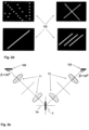
- Figure 2f shows the simulation results on the detecting element of the measuring device according to Figure 2e in two different cases, on a mirror-like surface and on a diffuse surface.
- the surface 2a of the object 2 is diffuse, also then further a strong position signal is obtained at a point where the virtual measuring plane 3 intersects the surface 2a of the object 2.
- the intensity distribution of light measured in an angle intersecting in respect of the axis of height of surface at the above-mentioned maximum point is narrow and clearly smaller than in case of the mirror surface.
- the shape of the intensity distribution differs clearly from the intensity distribution given by the mirror surface.
- the light is generated advantageously by a LED radiating white light (not shown in Figure 3 ), whereby light with sufficient wideband is obtained as to its wavelength distribution, the different wavelengths of which can be focused at different distances in direction of the optical axis.
- one exemplary output slit is shown in the output element 100 in the output element 100 in the output element 100 .
- the position of the output slit 102 c in the output element 100 is shown viewed in the direction of the optical axis of the illumination optics 111.
- the output slit 102 c is rotated by a rotation angle ⁇ in regard of the plane defined by the optical axes of the illumination optics 111 and the imaging optics 121.
- illumination optics 111 is produced an axial, chromatic aberration.
- the components ⁇ n (S), ⁇ n (R) of the red end of the light are in focus on the virtual measuring surface 3 under the surface 2 of the object, and, correspondingly, the components ⁇ 1 (S), ⁇ 1 (R) of the blue end of the light are in focus above the surface 2a.
- both the blue ends ⁇ 1 (S), ⁇ 1 (R) of the illumination and imaging are in focus in the upper edge of the virtual measuring surface 3. Accordingly, the red ends ⁇ n (S), ⁇ n (R) of the spectra are in focus in the bottom edge of the measuring surface (under the surface 2a in Figure 3 ).
- the height of the surface 2a has an effect on which component of the spectrum is reflected from the surface 2a.
- the colour of the component of the spectrum is not important in this embodiment, since the light signal reflected from surface 2a is detected advantageously by a black and white line or matrix sensor/camera.
- the position of surface 2a is indicated by the position of the maximum of the received signal on the sensor of the camera working as the indicator. The position of the received maximum signal is calibrated to correspond to a certain height of the surface 2a.
- both the illumination and imaging are shown in a symmetrical angle in regard of the surface 2a.
- the invention is however not restricted to this kind of a symmetrical measuring situation, but the edge of the illumination and imaging in regard of the surface 2a can be of different size without having an effect of the measuring event.
- the angle between illumination and imaging changes, nevertheless, in overlapping measuring regions there can always be found on measuring line where individual focus points can be found for different wavelengths.
- the light sensor of the imaging optics can be vertically against the optical axis 12a of the imaging optics.
- the size and shape of the measuring region can be freely defined with the used illumination and imaging optics.
- the size of the measuring region can advantageously be enlarged for the measuring sensor of the matrix camera.
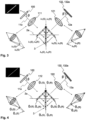
- Figure 4 shows the third advantageous embodiment of the invention whereby in providing confocality, spherical aberration is utilized.
- Figure 4 shows further an example of the meaning of spherical aberration.
- An exemplary lens 112 or 122 retracts the light to different focus points ⁇ 1 (S), ⁇ n (S) and ⁇ 1 (R), ⁇ n (R) on the grounds that where the light penetrates the lens 112 or 122.
- Light beams penetrating the lens at the centre have their focus point ⁇ n (S), ⁇ n (R) further away than the light beams penetrated on the outer edges of the lens.
- the height measuring is based on the spherical aberration of the lens or lenses and on the confocal imaging.
- the spherical aberration used is advantageously of the same size in imaging and in illumination.
- signals having the same angular aperture are imaged onto the measuring plane in direction of the normal of the surface.
- the measuring can be realized either with one wavelength or white light.
- the spherical aberration makes the optics to image the output slit in the output element 100 at different distances depending on the angular aperture of the optics. For example, light beams coming to a large angular aperture form an image close to the imaging optics 112, and accordingly, beams coming to a small incident angular aperture form an image farther away from the imaging optics 112.
- the output element 100 and the light sensor can be in a perpendicular angle in respect of the optical axis which is advantageous from the point of view of the structure of the device.
- the output slit 102 c and light sensor are utilized. Thanks to the spherical aberration, the image of output slit 102 c on the virtual measuring surface 3 is formed at different distances with different angular apertures ⁇ 1 (S), ⁇ n (S). Accordingly, the imaging optics 122 comprises the same property.
- the output element 100 and the light sensor need not to be inclined in relation to the axes 11a and 12a of the illumination optics 111 or imaging optics 121, but the image planes meet each other on the virtual measuring surface 3 with equal angular apertures ⁇ 1 (S), ⁇ 1 (R) and ⁇ n (S), ⁇ n (R).
- the output element 100 and the light sensor can be in a perpendicular angle in respect of the optical axis which is advantageous from the point of view of the structure of the device.
- a certain point of the light sensor of the imaging unit is calibrated to correspond to a certain height of surface 2a.
- Figure 5a shows an exemplary embodiment of the output or input element 100 or 130, whereby a linear variable filter 102 is utilized.
- a linear variable filter also known by LVF (Linear Variable Filter) lets at certain positions only a certain wavelength ⁇ 1 , ⁇ 2 , ⁇ n go through.
- LVF Linear Variable Filter
- Figure 5b shows the fourth advantageous embodiment of the invention, where in providing confocality a linear variable filter (LVF) is utilized both in illuminating and imaging.
- a LVF filter lets at different parts different wavelengths go through. At the one end of a LVF filter, shorter wavelengths are allowed to pass through, and at the other end, longer wavelengths can pass through.
- the light source of the illumination has to be a light source with a sufficient wideband as to its wavelength distribution (not shown in Figure 5b ), in order to be able to focus different wavelengths ⁇ 1 (S)-> ⁇ n (S) with illumination optics 113 to different positions onto the virtual measuring surface 3. From an image created onto the virtual measuring surface 3, with imaging optics 123 is obtained from surface 2a to the light sensor a local maximum signal, from which the distance to surface 2a can be defined.
- the output element 100 comprises a position-dependent linear variable filter 102a that comprises wavelengths ⁇ 1 -> ⁇ n .
- An image of the LVF filter is obtained in focus onto the virtual measuring surface 3 by inclining the output element 100 by angle ⁇ in relation to the optical axis 11a of the illumination optics 113.
- the angle ⁇ can advantageously be, for example, 135 degrees, whereby the focus region of the illumination hits the virtual measuring surface 3.
- the light sensor is advantageously of linear or rectangular shape, having in front of it as an input element a position-sensitive linear variable filter 102a.
- the LVF filter 102a also comprising the wavelengths ⁇ 1 -> ⁇ n , is inclined in respect of the optical axis 12a of the imaging optics by an angle ⁇ ', so that its image ⁇ 1 (R)-> ⁇ n (R) joins the plane of the image projected from the output element 102a onto the virtual measuring surface 3.
- the angle ⁇ ' can advantageously be, for example, 135 degrees, whereby the focus region of the illumination hits the virtual measuring surface 3.
- Figure 5c shows the measuring arrangement of Figure 5b in a perspective view.
- the different wavelengths ⁇ 1 -> ⁇ n of the LVF filter included in the output element are shown viewed from direction of the optical axis 11a of the illumination. Accordingly, the different wavelengths ⁇ 1 -> ⁇ n of the LVF filter 102a belonging to the output element are shown viewed from the direction of the optical axis 12a of the imaging.
- the measuring of the level of the height of the profile 2h0 can be realized.
- the method produces the measuring result 132h 0 of the surface, height profile of the surface, for the matrix detector 132a from the output element of the imaging for the width of the image projected to the object 2.
- a measurement of surface height profile of 1 000 pixels can be realized by using a CCD image sensor in size of 1 000 ⁇ 1 000 pixels as a light sensor.
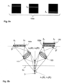
- Figure 6a shows the fifth advantageous embodiment of the invention in a side view.
- a linear variable filter (102a) is utilized both in the illumination and imaging.
- chromatic aberration is provided in the illumination optics 114 and imaging optics 124.
- a local maximum signal is obtained for detector 132a, from which the distance to surface 2a can be defined.
- a position-dependent linear variable filter 102a is utilized.
- a chromatic axial aberration of suitable size is provided, by means of which the image of the LVF filter 102a of the output element and the image of the LVF filter in front of the light sensor 132a of the imaging optics 124 is brought into focus by wavelengths on the virtual measuring surface 3.
- the angle of inclination ⁇ can thereby be 90 degrees.
- the angle of inclination ⁇ ' of the input element can thereby be 90 degrees, which makes the positioning of the light sensor and the imaging optics 124 easier in relation to each other.
- the blue ends ( ⁇ ) of the spectra of both the illumination and imaging are in focus in the upper edge of the virtual measuring surface 3. Accordingly, the red ends ( ⁇ n ) of the spectra are in focus in the bottom edge of the virtual measuring surface 3 (below the surface 2a in Figure 6a ).
- the height of the surface 2a has an effect on which wavelength of the spectrum is reflected from the surface 2a.
- a wavelength is reflected from the surface 2a that is in the common focus point of both the illumination and the imaging, this reflected wavelength penetrates the LVF filter 102a in front of the light sensor only at one position.
- the position of the component of the spectrum penetrated the LVF filter 102a is indicated, for example, by a black and white matrix camera.
- the position of the surface 2a is indicated by the position of the received maximum signal on the light sensor and not the wavelength of the received spectrum.
- the position of the received maximum signal on the light sensor is calibrated to correspond to a certain height of the surface 2a.
- the measuring of the surface height profile can be realized.
- a measuring device according to this embodiment produces a distance measurement result at the whole width of the image projected from the output slit to the object.
- a measurement of a distance profile of 1 000 pixels can be realized by using a CCD image sensor in size of 1 000 x 1 000 pixels as a light sensor.
- Figure 6b shows exemplary illumination optics 114 or imaging optics 124, a LVF filter 102a and a light source or light sensor, by which the embodiment of the invention according to Figure 6a can be realized.
- the frame 580 of the optics three lenses 581, 582 and 583 are mounted, by which both the axial chromatic aberration and the magnifications of lenses in direction of axes x and y are produced.
- an opening is indicated, against which the LVF filter 102a is fastened.
- the illumination optics 114 If it comes to the illumination optics 114, then in front of the LVF filter 102a there is, for example, a LED light source emitting white light.
- the light of the LED passes through the LVF filter 102a such that the different wavelengths of the white light get through only at certain positions in the LVF filter.
- Lenses 581, 582 and 583 modify the light A dispersed into different wavelengths of the spectrum passed through the LVF filter such that the result is an axial, chromatic aberration.
- a light sensor that may be a conventional CCD measuring sensor.
- the certain wavelength of the light B reflected from the surface 2a passes through the LVF filter 102a such that it penetrates the LVF filter 102a only at a certain position. This position of penetration of the wavelength is indicated by the CCD sensor.
- the certain position of the CCD sensor is calibrated to indicate a known height of the surface 2.
- the LVF filter shown in Figure 6b can be, for example, of type JDSU LVF4007003A, the filtering range of which is 400-700 nm. Dimensions of the filter
- Figure 7 shows in an exemplary flow chart main phases of a measuring method.
- the method according the invention is defined with claim 14.
- the method as indicated with Fig. 7 shares some features with the method of claim 14.
- a step 70 preceding the measuring the equipment belonging to the measuring arrangement are mounted into the object of measurement.
- the focus regions of both the illumination optics and the imaging optics are aligned with each other.
- it is defined or calibrated which height of surface is represented by the received position of the maximum signal in the measuring sensor.
- the light to be utilized in the measuring arrangement is generated.
- the light can be either monocromatic or wideband, for example white, light depending on the embodiment.
- a light source usually either a LED emitting one wavelength or a LED emitting white light is used.
- a light source region is generated for the output element 100 of the illumination that has an optimal geometric appearance from the point of view of the object of the measuring.
- the grated structure is provided by slits 102 made in the plane.
- one optical measuring signal is created that can be directed to the measuring plane that is substantially in the direction of the normal of the surface of the object of measurement.
- white light is utilized that is directed to the LVF filter 102a.
- the white light is dispersed into a spectrum with the LVF filter, and the dispersed spectrum is directed to a measuring plane in direction of the normal of the surface of the object of measurement.
- step 73 the image of the light source region created in step 72 is modified by the illumination optics.
- a virtual measuring surface 3 substantially intersecting the surface 2 to be measured, or a known group of focus points representing it, is provided.
- step 74 the image of the light source region modified by the illumination optics hits the surface 2 being the object of the measurement. Since the focus points formed by the illumination optics are on the virtual measurement surface 3, only one of the possible focus points hits the surface 2a to be measured, as the virtual measurement surface 3 intersects the surface 2a being the object of the measurement. From this focus point a light beam is reflected, the intensity of which is much higher than the light reflecting from the other locations of the surface 2a onto the imaging optics, since also the imaging optics has one focus point in the reflection point.
- step 75 the light beam is imaged from the surface 2a with the imaging optics onto the used position measuring means.
- the imaging optics is such that only the points on the virtual measuring surface 3 are in focus also on the detector means 130, 130a utilized in the imaging.
- the imaging optics comprises also a LVF filter 102a that can advantageously be utilized also as position indicating means.
- step 76 the light reflected from the surface 2a is received either with a line detector 132, a matrix detector 132a, a black and white camera or a colour camera.
- step 77 the position of the maximum value is defined from the received reflected light by detector means 132, 132a. Each individual position of maximum value on the detector means is calibrated to correspond a certain distance of the surface.
- step 78 it is checked whether also the optical properties of the surface 2a of the object 2 are measured. If other optical properties are not measured the process proceeds to step 79.
- step 79 it is checked whether there are several individual maximum values indicated from the light reflected from the received object 2. If there is only one maximum value, the measured value represents the distance of the surface being the object of the measurement.
- step 80 the distance of the reflection points from the surface is defined.
- the first indicated maximum value represents the height of the upper surface of the film and the last indicated maximum value represents the height of the bottom surface of the film.
- each of the other indicated maximum values represents an interface reflecting light inside the material to be measured. From the positions of the indicated maximums the thickness of each layer belonging to the film structure can be calculated.
- a partly translucent material does not include obvious separate films but is in its nature, for example, a diffusely scattering material, the signal produced by the method produces information about the intensity of light scattering from different depths. An object of measurement of this type could be, for example, skin.
- step 81 the scattering characteristics of the surface 2a are measured.
- the scattering characteristics are found out by measuring at the maximum reflection position that indicates the position of the surface also the intensity profile in one or more points in direction intersecting in relation to the position axis.
- the measured points included in the intensity profile of the light in this direction are proportional to the scattering characteristics of the surface 2a of the object 2.
- the measuring process proceeds to step 82.
- the intensity profile of the light is measured as some kind of a regional profile.
- step 82 An individual measuring process of the height of the surface ends in step 82. It is obvious for someone skilled in the art that the measuring process can return back to step 71 whereby a continuous measuring process is produced.
Landscapes
- Physics & Mathematics (AREA)
- General Physics & Mathematics (AREA)
- Health & Medical Sciences (AREA)
- General Health & Medical Sciences (AREA)
- Chemical & Material Sciences (AREA)
- Analytical Chemistry (AREA)
- Biochemistry (AREA)
- Life Sciences & Earth Sciences (AREA)
- Immunology (AREA)
- Pathology (AREA)
- Mathematical Physics (AREA)
- Electromagnetism (AREA)
- Engineering & Computer Science (AREA)
- Radar, Positioning & Navigation (AREA)
- Remote Sensing (AREA)
- Nuclear Medicine, Radiotherapy & Molecular Imaging (AREA)
- Radiology & Medical Imaging (AREA)
- Length Measuring Devices By Optical Means (AREA)
- Measurement Of Optical Distance (AREA)
Claims (18)
- Messvorrichtung (1, 5), die zum Messen einer Höhe und optischer Eigenschaften einer Oberfläche (2a, 2b) eines Objekts (2) mittels optischer Strahlung konfiguriert ist, wobei die Messvorrichtung Folgendes umfasst:- eine optische Beleuchtungseinheit (10), die eine Lichtquelle umfasst,- Beleuchtungsoptik (11, 110, 111, 112, 113, 114, 124), die angeordnet ist, um Licht der Lichtquelle auf das zu messende Objekt (2) zu richten,- eine Abbildungseinheit (13), und- Abbildungsoptik (12, 120, 121, 122, 123, 124), die so konfiguriert ist, dass sie reflektiertes oder gestreutes Licht von dem Objekt zu der Abbildungseinheit (13) sammelt, wobeidie Abbildungseinheit (13) dazu konfiguriert ist, eine Intensitätsverteilung des von dem Objekt (2) kommenden Lichts anzuzeigen,wobei- die Lichtquelle aus einem Ausgangselement (100) mit einem oder mehreren linienförmigen optischen Ausgangselementen (102) oder einer Gruppe von punktförmigen optischen Ausgangselementen (102) besteht, wobei die optischen Ausgangselemente eingerichtet sind, das Licht der Lichtquelle zumindest in einer Wellenlänge zu erzeugen,- die Abbildungseinheit (13) einen Lichtsensor umfasst, der aus einem oder mehreren linienförmigen, einer Gruppe von punktförmigen oder bereichsförmigen Detektorelementen (132, 132a) besteht, wobei die Abbildungseinheit (13) konfiguriert ist, um Intensitätswerte von Licht zu definieren, das an Punkten (K1(R)->Kn(R)) des Detektorelements (132, 132a) empfangbar ist, und den Ort der zu messenden Oberfläche (2a, 2b) aus der Position der maximalen Lichtintensität (Kx(R)) im Detektorelement (132, 132a) zu bestimmen, dadurch gekennzeichnet, dass- die Beleuchtungsoptik (11) und die Abbildungsoptik (12) so konfiguriert sind, dass sie konfokal gemeinsame Brennpunkte bilden, die eine virtuelle Messfläche (3) erzeugen, so dass ein von der Beleuchtungsoptik (11) aus Punkten (K1(S)->Kn(S)) des optischen Ausgangselements (102) der optischen Beleuchtungseinheit (10) gebildetes Bild mit einem Bild überlagert wird, das durch die Abbildungsoptik (12) aus den entsprechenden Punkten (K1(R)->Kn(R)) des Detektorelements (132, 132a) zumindest in einer gemeinsamen Wellenlänge (λ) oder Öffnungswinkel (θ) der Beleuchtungsoptik (11) und Abbildungsoptik (12) gebildet wird, wobei für jeden einzelnen Punkt (K1(S)->Kn(S)) des optischen Ausgangselements (102) und ein entsprechender Detektorpunkt (K1(R)->Kn(R)) maximal ein gemeinsamer Brennpunkt gebildet wird, und wobei sich jeder der gemeinsamen Brennpunkte auf einer anderen geometrischen Ebene parallel zu einer Ebene befindet, die durch eine optische Achse (12a) der Abbildungsoptik (12) und eine optische Achse (11a) der Beleuchtungsoptik (11) definiert ist.
- Messvorrichtung nach Anspruch 1, wobei die Messvorrichtung ferner Mittel zum Definieren eines Glanzgrades oder optischer Eigenschaften der zu messenden Oberfläche (2a, 2b) in einem Bereich umfasst, der den Bereich maximaler Intensität umgibt, der die Position der Oberfläche (2a, 2b) aus einer Verteilung der Intensitätswerte (P1(R), Pn(R)) des gemessenen Lichts angibt.
- Messvorrichtung nach Anspruch 1, wobei die virtuelle Messfläche (3) eine der folgenden ist: eine Ebene, eine gekrümmte Fläche, eine Linie, ein Satz von Linien oder eine Gruppe von Punkten.
- Messvorrichtung nach Anspruch 1, wobei das Ausgangselement (100) der optischen Beleuchtungseinheit (10) ein oder mehrere optische Ausgangselemente (102) mit linienförmigen Ausgangsschlitzen (102c) umfasst, die einen Drehwinkel α der linienförmigen Austrittsschlitze (102c) mit der durch die optische Achse (11a) der Beleuchtungsoptik (11) und die optische Achse (12a) der Abbildungsoptik aufgespannten Ebene bilden, und der Drehwinkel α mehr als 0 bis 90 Grad beträgt.
- Messvorrichtung nach Anspruch 4, dadurch gekennzeichnet, dass die optische Lichtquelle einen Neigungswinkel β zur optischen Achse (11a) der Beleuchtungsoptik (11) bildet und durch diesen Neigungswinkel β die Beleuchtungsoptik (11) konfiguriert ist, das Bild der Ausgangsschlitze (102c) auf die virtuelle Messfläche (3) zu fokussieren.
- Messvorrichtung nach einem der Ansprüche 1 bis 3, wobei in der Beleuchtungsoptik (11) und Abbildungsoptik (12) eine längliche chromatische Aberration vorgesehen ist, so dass das von der Beleuchtungsoptik (11) von den Ausgangsschlitzen (102c) gebildete Bild und das von der Abbildungsoptik (12) von dem Detektorelement (132, 132a) gebildete Bild in der virtuellen Messfläche (3) zumindest auf einigen gemeinsamen Wellenlängen (λn(S), λn(R)) überlappen, wenn es zu ihren entsprechenden Punkten kommt.
- Messvorrichtung nach einem der Ansprüche 1 bis 3, wobei in der Beleuchtungsoptik (11) und Abbildungsoptik (12) eine sphärische Aberration vorgesehen ist, so dass das von der Beleuchtungsoptik (11) von den Ausgangsschlitzen (102c) gebildete Bild und das von der Abbildungsoptik (12) von dem Detektorelement (132, 132a) gebildete Bild in der virtuellen Messfläche (3) zumindest auf einigen gemeinsamen Öffnungswinkeln (θn(S), θn(R)) überlappen, wenn es zu ihren entsprechenden Punkten kommt.
- Messvorrichtung nach Anspruch 1, wobei- die optische Beleuchtungseinheit (10) eine Lichtquelle mit nicht-monochromatischem Licht umfasst und das Ausgangselement (100) einen positionsabhängigen linear variablen Filter (102a) umfasst,- das Detektorelement (132) auch einen positionsabhängigen linear variablen Filter (102a) umfasst, wobei die entsprechenden Punkte des Detektorelements die gleiche Wellenlänge (λ1, λn) des Durchlassbereichs aufweisen wie die entsprechenden Punkte des linearen variablen Filters (102a) des Lichtquellen-Ausgangselements (100)- das Ausgangselement (100) gegenüber der optischen Achse (11a) der Beleuchtungsoptik (11) um den Neigungswinkel β geneigt ist, und auch das Detektorelement (132) um den entsprechenden Neigungswinkel β' geneigt ist, so dass ein Punkt des linearen variablen Filters (102a) des Ausgangselements (100) und der entsprechende Punkt des linearen variablen Filters (102a) des Eingangselements (130) einen gemeinsamen Brennpunkt auf der virtuellen Messfläche (3) auf gleichen gemeinsamen Wellenlängen (λn(S), λn(R)) haben.
- Messvorrichtung nach Anspruch 1, wobei- die optische Beleuchtungseinheit (10) eine Lichtquelle mit nicht-monochromatischem Licht umfasst, und das Ausgangselement (100) ein positionsabhängig linear variables Filter (102a) umfasst- das Eingangselement (130) auch einen positionsabhängigen linear variablen Filter (102a) umfasst, dessen entsprechende Punkte die gleiche Wellenlänge (λ1, λn) des Durchlassbereichs haben wie die entsprechenden Punkte des linearen variablen Filters (102a) des Ausgangselements (100)- in der Beleuchtungsoptik (11) und Abbildungsoptik (12) eine längliche chromatische Aberration vorgesehen ist, so dass der Punkt des linearen variablen Filters (102a) des Ausgangselements (100) und der entsprechende Punkt des linearen variablen Filters (102a) des Eingangselements (130) einen gemeinsamen Brennpunkt auf der virtuellen Messfläche (3) auf gleichen gemeinsamen Wellenlängen (An(S), λn(R)) haben.
- Messvorrichtung nach Anspruch 1, wobei das Lichtdetektorelement (132, 132a) eine Zeilenkamera, eine Matrixkamera oder ein Massenzentrumsdetektor für Licht ist.
- Messvorrichtung nach Anspruch 1, dadurch gekennzeichnet, dass bei der Messung eines optisch transparenten Objekts (2) jede interne oder externe Grenzfläche (2a, 2b) des Objekts (2) ein separates Maximalsignal (h0, h1) erzeugt, aus dessen Differenz die Messvorrichtung (1) eingerichtet ist, eine Dicke des transparenten Objekts (2) zu bestimmen.
- Messvorrichtung nach Anspruch 11, dadurch gekennzeichnet, dass aus einer Intensitätsverteilung des aus dem Inneren des Objekts (2) gestreuten/gestreuten Lichts eine innere Struktur des Objekts (2) von der Intensität des Lichts bestimmt werden kann, das in verschiedenen Tiefen gestreut wird.
- Messanordnung zum Messen einer Dicke eines Messobjekts (2), umfassend eine erste Messvorrichtung (1) zum Messen einer ersten Oberfläche (2a) und eine zweite Messvorrichtung (5) zum Messen einer zweiten Oberfläche (2b), wobei beide Messvorrichtungen Anspruch 1 entsprechen und die erste Messanordnung (1) konfiguriert ist, um eine Höhe einer oberen Oberfläche (2a) des Objekts zu messen, und die zweite Messvorrichtung (5) dazu konfiguriert ist, eine Höhe einer Bodenfläche (2b) des Objekts zu messen, und eine Differenz zwischen den Messergebnissen konfiguriert ist, in einer Messanordnung als eine Dicke des Objekts angezeigt zu werden.
- Verfahren zum optischen Messen einer Höhe einer Oberfläche (2a) eines Objekts (2), wobei eine optische Beleuchtung und optische Abbildung der Oberfläche des Objekts zweiachsig mit mindestens einer Wellenlänge erfolgt, so dass sowohl die Beleuchtung als auch die Abbildung aus unterschiedlichen Richtungen auf die Oberfläche gerichtet sind, wobei die Abbildung und die Beleuchtung konfokal realisiert werden, indem sie gemeinsame Brennpunkte bilden, die eine virtuelle Messoberfläche (3) erzeugen, die mit der Oberfläche (2a, 2b) des Objekts (2) zu schneiden ist, wodurchdie Beleuchtung bereitgestellt wird, indem ein Bild durch die Beleuchtungsoptik (11) von Punkten (K1(S)->Kn(S)) eines oder mehrerer linienartiger optischer Ausgangselemente (102) oder einer Gruppe von punktförmigen optischen Ausgangselementen (102) eines Ausgangselements (100) einer optischen Beleuchtungseinheit (10) gebildet wird, die konfiguriert sind, um Licht zumindest in einer Wellenlänge zu erzeugen, die Abbildung durch eine Abbildung durch die Abbildungsoptik (12) aus den entsprechenden Punkten (K1(R)->Kn(R)) eines linien- oder bereichsförmigen Detektorelements (132, 132a) einer Abbildungseinheit (13) erfolgt, wodurchdas aus den Punkten (K1(S) ->Kn(S)) des optischen Ausgangselements (102) gebildete Bild so angeordnet ist, dass es sich mit dem Bild überlappt, das aus den entsprechenden Punkten (K1(R)->Kn(R)) des Detektorelements (132, 132a) zumindest in einer gemeinsamen Wellenlänge (λ) oder Öffnungswinkel (θ) von Beleuchtungsoptik (11) und Abbildungsoptik (12) in der virtuellen Messfläche (3) gebildet wird, und wodurch für jeden einzelnen Punkt (K1(S)->Kn(S)) des optischen Ausgangselements (102) und einen entsprechenden Detektorpunkt (K1(R)->Kn(R)) maximal ein gemeinsamer Brennpunkt gebildet wird, wobei sich jeder der gemeinsamen Brennpunkte auf einer anderen geometrischen Ebene parallel zu einer Ebene befindet, die durch eine optische Achse (12a) der Abbildungsoptik (12) und eine optische Achse (11a) der Beleuchtungsoptik (11) definiert ist,und wobei Intensitätswerte des an den Punkten (K1(R)->Kn(R)) des Detektorelements (132, 132a) empfangenen Lichts definiert sind und der Ort der Oberfläche (2a, 2b) aus der Position (Kx(R)) der maximalen Lichtintensität im Detektorelement (132, 132a) durch die Abbildungseinheit (13) angezeigt wird.
- Verfahren nach Anspruch 14, wobei ein optisches Lichtmuster durch Beleuchten (71, 72) eines oder mehrerer linienartiger Ausgangsschlitze (102c) des optischen Ausgangselements (102) erzeugt wird, das von ihnen erzeugte Bild durch eine Beleuchtungsoptik (11) modifiziert wird (73), so dass verschiedene Teile (K1(S), Kn(S)) eines Lichtmusters (11b, 31), das durch die Ausgangsschlitze (102c) erzeugt wird, an verschiedenen Positionen auf der virtuellen Messoberfläche (3) fokussiert sind.
- Verfahren nach Anspruch 14, wobei die Beleuchtungsoptik (11, 111, 112) das durch die Ausgangsschlitze (102c) erzeugte optische Lichtmuster auf die virtuelle Messfläche (3) fokussiert, indem entweder chromatische Aberration oder sphärische Aberration verwendet wird.
- Verfahren nach Anspruch 15, wobei die Abbildungsoptik (12, 121, 122) zur Erzielung von Konfokalität einen Reflexionspunkt abbildet, der am Schnittpunkt des Bildes (11b, 31) des Austrittsspaltes (102c) auf der virtuellen Messfläche (3) und der Oberfläche (2a, 2b) des Objekts (2) durch das Eingangselement (130) auf ein Detektorelement (132, 132a) erzeugt wird, indem entweder chromatische Aberration oder sphärische Aberration verwendet werden.
- Verfahren nach Anspruch 14, wobei nichtmonochromatisches Licht mit einem positionsabhängigen linear variablen Filter (102a) vor der Beleuchtungsoptik (113) gefiltert wird und das Bild des Ausgangsschlitzes, das durch das positionsabhängige lineare variable Filter (102a) erzeugt wird, von der Beleuchtungsoptik (113) auf die virtuelle Messfläche (3) abgebildet wird, und eine Lichtwellenlänge (λ1, λn), die von einem Schnittpunkt der Oberfläche (2a, 2b) des Objekts (2) reflektiert wird, nach der Abbildungsoptik (123) durch ein positionsabhängiges linear variables Filter (102a) auf ein Detektorelement (132, 132a) abgebildet werden.
Applications Claiming Priority (2)
| Application Number | Priority Date | Filing Date | Title |
|---|---|---|---|
| FI20125958A FI125408B (fi) | 2012-09-17 | 2012-09-17 | Menetelmä ja mittalaite pinnan etäisyyden, kohteen paksuuden ja optisten ominaisuuksien mittaamiseksi |
| PCT/FI2013/050898 WO2014041254A1 (en) | 2012-09-17 | 2013-09-17 | Method and measuring device for measuring the distance of a surface, thickness and optical properties of an object |
Publications (4)
| Publication Number | Publication Date |
|---|---|
| EP2901102A1 EP2901102A1 (de) | 2015-08-05 |
| EP2901102A4 EP2901102A4 (de) | 2016-04-20 |
| EP2901102C0 EP2901102C0 (de) | 2023-06-07 |
| EP2901102B1 true EP2901102B1 (de) | 2023-06-07 |
Family
ID=50277691
Family Applications (1)
| Application Number | Title | Priority Date | Filing Date |
|---|---|---|---|
| EP13837251.1A Active EP2901102B1 (de) | 2012-09-17 | 2013-09-17 | Verfahren und messvorrichtung zur messung des oberflächenabstands, der dicke und der optischen eigenschaften eines objekts |
Country Status (6)
| Country | Link |
|---|---|
| US (1) | US9476707B2 (de) |
| EP (1) | EP2901102B1 (de) |
| ES (1) | ES2947564T3 (de) |
| FI (1) | FI125408B (de) |
| PL (1) | PL2901102T3 (de) |
| WO (1) | WO2014041254A1 (de) |
Families Citing this family (10)
| Publication number | Priority date | Publication date | Assignee | Title |
|---|---|---|---|---|
| FI127908B (en) * | 2015-09-22 | 2019-05-15 | Teknologian Tutkimuskeskus Vtt Oy | Method and apparatus for measuring the height of a surface |
| CN105890625B (zh) * | 2016-04-05 | 2018-12-21 | 北京控制工程研究所 | 一种基于碳纳米管遮光罩的星敏感器的杂光测试方法 |
| TWI616641B (zh) * | 2017-02-23 | 2018-03-01 | Method for measuring wafer thickness using near infrared ray | |
| JP6821526B2 (ja) * | 2017-08-15 | 2021-01-27 | キヤノン株式会社 | 画像処理方法、画像処理装置、撮像装置、および、プログラム |
| JPWO2019065484A1 (ja) * | 2017-09-28 | 2020-11-12 | パイオニア株式会社 | 測距装置及び光走査装置 |
| US11287626B2 (en) | 2019-05-17 | 2022-03-29 | Hong Kong Applied Science and Technology Research Institute Comoanv Limited | Chromatic confocal system and a method for inspecting an object |
| FI130557B (en) * | 2020-09-29 | 2023-11-17 | Lmi Tech Inc | Device for determining a distance, surface thickness and optical properties of an object and related method |
| CN113959349B (zh) * | 2021-10-25 | 2022-04-19 | 湖南捷力泰科技有限公司 | 一种膜片质量检测装置及其方法 |
| DE102022202778B4 (de) * | 2022-02-11 | 2024-05-16 | Micro-Epsilon Optronic Gmbh | System und Verfahren zur konfokal-chromatischen Linienabstandsmessung |
| US20250116506A1 (en) | 2022-02-11 | 2025-04-10 | Micro-Epsilon Optronic Gmbh | System and method for confocal-chromatic line distance measurement |
Family Cites Families (17)
| Publication number | Priority date | Publication date | Assignee | Title |
|---|---|---|---|---|
| DE2906641A1 (de) | 1979-02-21 | 1980-08-28 | Freudenberg Carl Fa | Verfahren zur optisch-elektrischen messung des abstandes zwischen einer messeinrichtung und einem pruefling |
| US4936676A (en) | 1984-11-28 | 1990-06-26 | Honeywell Inc. | Surface position sensor |
| IL121267A0 (en) | 1997-07-09 | 1998-01-04 | Yeda Res & Dev | Method and device for determining the profile of an object |
| EP0890822A3 (de) * | 1997-07-09 | 2000-04-05 | YEDA RESEARCH AND DEVELOPMENT Co. LTD. | Triangulationsverfahren und optisches farbkodiertes Profilometriesystem |
| US6573998B2 (en) | 1997-11-06 | 2003-06-03 | Cynovad, Inc. | Optoelectronic system using spatiochromatic triangulation |
| KR100406843B1 (ko) * | 2001-04-06 | 2003-11-21 | (주) 인텍플러스 | 색정보를 이용한 실시간 3차원 표면형상 측정방법 및 장치 |
| AU2003236291A1 (en) * | 2002-03-28 | 2003-10-27 | Matsuuradenkosha Company Limited | Evaluation method and device for gel state or sol-gel state change of object |
| FR2848664B1 (fr) | 2002-12-11 | 2005-03-11 | Micro Module | Detecteur de position, forme et reflectivite d'une surface |
| TWI245114B (en) * | 2004-10-11 | 2005-12-11 | Ind Tech Res Inst | Apparatus for measuring imaging spectrograph |
| US20060232790A1 (en) | 2005-04-18 | 2006-10-19 | Lee Chase | Confocal measurement method and apparatus in a paper machine |
| JP2007147299A (ja) | 2005-11-24 | 2007-06-14 | Kobe Steel Ltd | 変位測定装置及び変位測定方法 |
| US20070263228A1 (en) | 2006-05-12 | 2007-11-15 | Voith Paper Patent Gmbh | Device and process for optical distance measurement |
| FI119259B (fi) * | 2006-10-18 | 2008-09-15 | Valtion Teknillinen | Pinnan ja paksuuden määrittäminen |
| US20080137061A1 (en) | 2006-12-07 | 2008-06-12 | Christopher John Rush | Displacement Measurement Sensor Using the Confocal Principle |
| EP2124085A4 (de) | 2007-02-14 | 2010-04-28 | Nikon Corp | Konfokales schlitzrastermikroskop |
| FI124299B (fi) * | 2009-10-08 | 2014-06-13 | Focalspec Oy | Mittalaite ja menetelmä kohteen ja kohteen pinnan ominaisuuksien mittaamiseksi |
| TWI414817B (zh) * | 2010-07-23 | 2013-11-11 | Univ Nat Taipei Technology | 線型彩色共焦顯微系統 |
-
2012
- 2012-09-17 FI FI20125958A patent/FI125408B/fi active IP Right Grant
-
2013
- 2013-09-17 US US14/427,127 patent/US9476707B2/en active Active
- 2013-09-17 WO PCT/FI2013/050898 patent/WO2014041254A1/en not_active Ceased
- 2013-09-17 ES ES13837251T patent/ES2947564T3/es active Active
- 2013-09-17 EP EP13837251.1A patent/EP2901102B1/de active Active
- 2013-09-17 PL PL13837251.1T patent/PL2901102T3/pl unknown
Also Published As
| Publication number | Publication date |
|---|---|
| ES2947564T3 (es) | 2023-08-11 |
| FI20125958A7 (fi) | 2014-03-18 |
| EP2901102C0 (de) | 2023-06-07 |
| PL2901102T3 (pl) | 2023-11-20 |
| EP2901102A4 (de) | 2016-04-20 |
| US20150219454A1 (en) | 2015-08-06 |
| WO2014041254A1 (en) | 2014-03-20 |
| US9476707B2 (en) | 2016-10-25 |
| EP2901102A1 (de) | 2015-08-05 |
| FI125408B (fi) | 2015-09-30 |
Similar Documents
| Publication | Publication Date | Title |
|---|---|---|
| EP2901102B1 (de) | Verfahren und messvorrichtung zur messung des oberflächenabstands, der dicke und der optischen eigenschaften eines objekts | |
| US5165063A (en) | Device for measuring distances using an optical element of large chromatic aberration | |
| US7561273B2 (en) | Device and method for measurement of surfaces | |
| FI124299B (fi) | Mittalaite ja menetelmä kohteen ja kohteen pinnan ominaisuuksien mittaamiseksi | |
| US20140043619A1 (en) | Chromatic confocal scanning apparatus | |
| US9509893B2 (en) | Imaging device and analyzing apparatus using the imaging device | |
| KR20140096115A (ko) | 검사용 조명 장치 및 검사용 조명 방법 | |
| KR101794641B1 (ko) | 파장 분리를 이용한 높이 및 형상측정이 가능한 경사 분광시스템 | |
| JP7411682B2 (ja) | 光シート顕微鏡および試料空間内の物体の屈折率を特定するための方法 | |
| EP3353489B1 (de) | Verfahren und vorrichtung zur messung der höhe einer oberfläche | |
| US20250116506A1 (en) | System and method for confocal-chromatic line distance measurement | |
| JP2014048096A (ja) | 二次元分光計測装置及び二次元分光計測方法 | |
| JP7641391B2 (ja) | 物体の距離、表面厚さ、及び光学特性を決定する装置と関連方法 | |
| JP7669039B2 (ja) | 分光測定装置 | |
| CA3193114C (en) | Device for determining a distance, surface thickness and optical properties of an object and related method | |
| CN210070874U (zh) | 超光谱线扫描3d测量装置 | |
| JPWO2018092248A1 (ja) | 標本形状測定装置 | |
| JP7458617B1 (ja) | 検査用照明装置及び照明光学系及び検査システム | |
| TWM568363U (zh) | Hyperspectral image detecting device and detecting device | |
| HK40099084B (en) | Device for determining a distance, surface thickness and optical properties of an object and related method | |
| HK40099084A (en) | Device for determining a distance, surface thickness and optical properties of an object and related method | |
| TW202601069A (zh) | 光學感測器 | |
| JP2009074876A (ja) | 計測装置およびその計測方法 |
Legal Events
| Date | Code | Title | Description |
|---|---|---|---|
| PUAI | Public reference made under article 153(3) epc to a published international application that has entered the european phase |
Free format text: ORIGINAL CODE: 0009012 |
|
| 17P | Request for examination filed |
Effective date: 20150413 |
|
| AK | Designated contracting states |
Kind code of ref document: A1 Designated state(s): AL AT BE BG CH CY CZ DE DK EE ES FI FR GB GR HR HU IE IS IT LI LT LU LV MC MK MT NL NO PL PT RO RS SE SI SK SM TR |
|
| AX | Request for extension of the european patent |
Extension state: BA ME |
|
| DAX | Request for extension of the european patent (deleted) | ||
| RA4 | Supplementary search report drawn up and despatched (corrected) |
Effective date: 20160317 |
|
| RIC1 | Information provided on ipc code assigned before grant |
Ipc: G01N 21/57 20060101ALI20160311BHEP Ipc: G01B 9/02 20060101ALI20160311BHEP Ipc: G01B 11/06 20060101AFI20160311BHEP |
|
| STAA | Information on the status of an ep patent application or granted ep patent |
Free format text: STATUS: EXAMINATION IS IN PROGRESS |
|
| 17Q | First examination report despatched |
Effective date: 20170303 |
|
| RAP1 | Party data changed (applicant data changed or rights of an application transferred) |
Owner name: LMI TECHNOLOGIES OY |
|
| RAP1 | Party data changed (applicant data changed or rights of an application transferred) |
Owner name: LMI TECHNOLOGIES INC. |
|
| GRAP | Despatch of communication of intention to grant a patent |
Free format text: ORIGINAL CODE: EPIDOSNIGR1 |
|
| STAA | Information on the status of an ep patent application or granted ep patent |
Free format text: STATUS: GRANT OF PATENT IS INTENDED |
|
| RIC1 | Information provided on ipc code assigned before grant |
Ipc: G01N 21/49 20060101ALN20220517BHEP Ipc: G01N 21/84 20060101ALI20220517BHEP Ipc: G01N 21/57 20060101ALI20220517BHEP Ipc: G01N 21/47 20060101ALI20220517BHEP Ipc: G01B 11/06 20060101AFI20220517BHEP |
|
| INTG | Intention to grant announced |
Effective date: 20220601 |
|
| GRAJ | Information related to disapproval of communication of intention to grant by the applicant or resumption of examination proceedings by the epo deleted |
Free format text: ORIGINAL CODE: EPIDOSDIGR1 |
|
| STAA | Information on the status of an ep patent application or granted ep patent |
Free format text: STATUS: EXAMINATION IS IN PROGRESS |
|
| GRAP | Despatch of communication of intention to grant a patent |
Free format text: ORIGINAL CODE: EPIDOSNIGR1 |
|
| STAA | Information on the status of an ep patent application or granted ep patent |
Free format text: STATUS: GRANT OF PATENT IS INTENDED |
|
| INTC | Intention to grant announced (deleted) | ||
| RIC1 | Information provided on ipc code assigned before grant |
Ipc: G01N 21/49 20060101ALN20220816BHEP Ipc: G01N 21/84 20060101ALI20220816BHEP Ipc: G01N 21/57 20060101ALI20220816BHEP Ipc: G01N 21/47 20060101ALI20220816BHEP Ipc: G01B 11/06 20060101AFI20220816BHEP |
|
| INTG | Intention to grant announced |
Effective date: 20220913 |
|
| GRAS | Grant fee paid |
Free format text: ORIGINAL CODE: EPIDOSNIGR3 |
|
| GRAA | (expected) grant |
Free format text: ORIGINAL CODE: 0009210 |
|
| STAA | Information on the status of an ep patent application or granted ep patent |
Free format text: STATUS: THE PATENT HAS BEEN GRANTED |
|
| AK | Designated contracting states |
Kind code of ref document: B1 Designated state(s): AL AT BE BG CH CY CZ DE DK EE ES FI FR GB GR HR HU IE IS IT LI LT LU LV MC MK MT NL NO PL PT RO RS SE SI SK SM TR |
|
| REG | Reference to a national code |
Ref country code: GB Ref legal event code: FG4D |
|
| REG | Reference to a national code |
Ref country code: CH Ref legal event code: EP Ref country code: AT Ref legal event code: REF Ref document number: 1576329 Country of ref document: AT Kind code of ref document: T Effective date: 20230615 Ref country code: DE Ref legal event code: R096 Ref document number: 602013083973 Country of ref document: DE |
|
| U01 | Request for unitary effect filed |
Effective date: 20230607 |
|
| U07 | Unitary effect registered |
Designated state(s): AT BE BG DE DK EE FI FR IT LT LU LV MT NL PT SE SI Effective date: 20230612 |
|
| REG | Reference to a national code |
Ref country code: ES Ref legal event code: FG2A Ref document number: 2947564 Country of ref document: ES Kind code of ref document: T3 Effective date: 20230811 |
|
| REG | Reference to a national code |
Ref country code: LT Ref legal event code: MG9D |
|
| U20 | Renewal fee for the european patent with unitary effect paid |
Year of fee payment: 11 Effective date: 20230918 |
|
| PG25 | Lapsed in a contracting state [announced via postgrant information from national office to epo] |
Ref country code: NO Free format text: LAPSE BECAUSE OF FAILURE TO SUBMIT A TRANSLATION OF THE DESCRIPTION OR TO PAY THE FEE WITHIN THE PRESCRIBED TIME-LIMIT Effective date: 20230907 |
|
| PG25 | Lapsed in a contracting state [announced via postgrant information from national office to epo] |
Ref country code: RS Free format text: LAPSE BECAUSE OF FAILURE TO SUBMIT A TRANSLATION OF THE DESCRIPTION OR TO PAY THE FEE WITHIN THE PRESCRIBED TIME-LIMIT Effective date: 20230607 Ref country code: HR Free format text: LAPSE BECAUSE OF FAILURE TO SUBMIT A TRANSLATION OF THE DESCRIPTION OR TO PAY THE FEE WITHIN THE PRESCRIBED TIME-LIMIT Effective date: 20230607 Ref country code: GR Free format text: LAPSE BECAUSE OF FAILURE TO SUBMIT A TRANSLATION OF THE DESCRIPTION OR TO PAY THE FEE WITHIN THE PRESCRIBED TIME-LIMIT Effective date: 20230908 |
|
| PG25 | Lapsed in a contracting state [announced via postgrant information from national office to epo] |
Ref country code: SK Free format text: LAPSE BECAUSE OF FAILURE TO SUBMIT A TRANSLATION OF THE DESCRIPTION OR TO PAY THE FEE WITHIN THE PRESCRIBED TIME-LIMIT Effective date: 20230607 |
|
| PG25 | Lapsed in a contracting state [announced via postgrant information from national office to epo] |
Ref country code: IS Free format text: LAPSE BECAUSE OF FAILURE TO SUBMIT A TRANSLATION OF THE DESCRIPTION OR TO PAY THE FEE WITHIN THE PRESCRIBED TIME-LIMIT Effective date: 20231007 |
|
| PG25 | Lapsed in a contracting state [announced via postgrant information from national office to epo] |
Ref country code: SM Free format text: LAPSE BECAUSE OF FAILURE TO SUBMIT A TRANSLATION OF THE DESCRIPTION OR TO PAY THE FEE WITHIN THE PRESCRIBED TIME-LIMIT Effective date: 20230607 Ref country code: SK Free format text: LAPSE BECAUSE OF FAILURE TO SUBMIT A TRANSLATION OF THE DESCRIPTION OR TO PAY THE FEE WITHIN THE PRESCRIBED TIME-LIMIT Effective date: 20230607 Ref country code: RO Free format text: LAPSE BECAUSE OF FAILURE TO SUBMIT A TRANSLATION OF THE DESCRIPTION OR TO PAY THE FEE WITHIN THE PRESCRIBED TIME-LIMIT Effective date: 20230607 Ref country code: IS Free format text: LAPSE BECAUSE OF FAILURE TO SUBMIT A TRANSLATION OF THE DESCRIPTION OR TO PAY THE FEE WITHIN THE PRESCRIBED TIME-LIMIT Effective date: 20231007 Ref country code: CZ Free format text: LAPSE BECAUSE OF FAILURE TO SUBMIT A TRANSLATION OF THE DESCRIPTION OR TO PAY THE FEE WITHIN THE PRESCRIBED TIME-LIMIT Effective date: 20230607 |
|
| REG | Reference to a national code |
Ref country code: DE Ref legal event code: R097 Ref document number: 602013083973 Country of ref document: DE |
|
| PLBE | No opposition filed within time limit |
Free format text: ORIGINAL CODE: 0009261 |
|
| STAA | Information on the status of an ep patent application or granted ep patent |
Free format text: STATUS: NO OPPOSITION FILED WITHIN TIME LIMIT |
|
| REG | Reference to a national code |
Ref country code: CH Ref legal event code: PL |
|
| 26N | No opposition filed |
Effective date: 20240308 |
|
| PG25 | Lapsed in a contracting state [announced via postgrant information from national office to epo] |
Ref country code: MC Free format text: LAPSE BECAUSE OF FAILURE TO SUBMIT A TRANSLATION OF THE DESCRIPTION OR TO PAY THE FEE WITHIN THE PRESCRIBED TIME-LIMIT Effective date: 20230607 |
|
| REG | Reference to a national code |
Ref country code: IE Ref legal event code: MM4A |
|
| PG25 | Lapsed in a contracting state [announced via postgrant information from national office to epo] |
Ref country code: IE Free format text: LAPSE BECAUSE OF NON-PAYMENT OF DUE FEES Effective date: 20230917 |
|
| PG25 | Lapsed in a contracting state [announced via postgrant information from national office to epo] |
Ref country code: CH Free format text: LAPSE BECAUSE OF NON-PAYMENT OF DUE FEES Effective date: 20230930 |
|
| PG25 | Lapsed in a contracting state [announced via postgrant information from national office to epo] |
Ref country code: IE Free format text: LAPSE BECAUSE OF NON-PAYMENT OF DUE FEES Effective date: 20230917 Ref country code: CH Free format text: LAPSE BECAUSE OF NON-PAYMENT OF DUE FEES Effective date: 20230930 |
|
| U20 | Renewal fee for the european patent with unitary effect paid |
Year of fee payment: 12 Effective date: 20240927 |
|
| PG25 | Lapsed in a contracting state [announced via postgrant information from national office to epo] |
Ref country code: CY Free format text: LAPSE BECAUSE OF FAILURE TO SUBMIT A TRANSLATION OF THE DESCRIPTION OR TO PAY THE FEE WITHIN THE PRESCRIBED TIME-LIMIT; INVALID AB INITIO Effective date: 20130917 |
|
| PG25 | Lapsed in a contracting state [announced via postgrant information from national office to epo] |
Ref country code: HU Free format text: LAPSE BECAUSE OF FAILURE TO SUBMIT A TRANSLATION OF THE DESCRIPTION OR TO PAY THE FEE WITHIN THE PRESCRIBED TIME-LIMIT; INVALID AB INITIO Effective date: 20130917 |
|
| PGFP | Annual fee paid to national office [announced via postgrant information from national office to epo] |
Ref country code: PL Payment date: 20250904 Year of fee payment: 13 |
|
| PGFP | Annual fee paid to national office [announced via postgrant information from national office to epo] |
Ref country code: GB Payment date: 20250929 Year of fee payment: 13 |
|
| U20 | Renewal fee for the european patent with unitary effect paid |
Year of fee payment: 13 Effective date: 20250929 |
|
| PG25 | Lapsed in a contracting state [announced via postgrant information from national office to epo] |
Ref country code: TR Free format text: LAPSE BECAUSE OF FAILURE TO SUBMIT A TRANSLATION OF THE DESCRIPTION OR TO PAY THE FEE WITHIN THE PRESCRIBED TIME-LIMIT Effective date: 20230607 |
|
| PGFP | Annual fee paid to national office [announced via postgrant information from national office to epo] |
Ref country code: ES Payment date: 20251001 Year of fee payment: 13 |