EP2896718A1 - Method for manufacturing heat resistant composite material and manufacturing device - Google Patents
Method for manufacturing heat resistant composite material and manufacturing device Download PDFInfo
- Publication number
- EP2896718A1 EP2896718A1 EP13879446.6A EP13879446A EP2896718A1 EP 2896718 A1 EP2896718 A1 EP 2896718A1 EP 13879446 A EP13879446 A EP 13879446A EP 2896718 A1 EP2896718 A1 EP 2896718A1
- Authority
- EP
- European Patent Office
- Prior art keywords
- heat
- composite material
- resistant composite
- gas
- silicon carbide
- Prior art date
- Legal status (The legal status is an assumption and is not a legal conclusion. Google has not performed a legal analysis and makes no representation as to the accuracy of the status listed.)
- Withdrawn
Links
Images




Classifications
-
- C—CHEMISTRY; METALLURGY
- C23—COATING METALLIC MATERIAL; COATING MATERIAL WITH METALLIC MATERIAL; CHEMICAL SURFACE TREATMENT; DIFFUSION TREATMENT OF METALLIC MATERIAL; COATING BY VACUUM EVAPORATION, BY SPUTTERING, BY ION IMPLANTATION OR BY CHEMICAL VAPOUR DEPOSITION, IN GENERAL; INHIBITING CORROSION OF METALLIC MATERIAL OR INCRUSTATION IN GENERAL
- C23C—COATING METALLIC MATERIAL; COATING MATERIAL WITH METALLIC MATERIAL; SURFACE TREATMENT OF METALLIC MATERIAL BY DIFFUSION INTO THE SURFACE, BY CHEMICAL CONVERSION OR SUBSTITUTION; COATING BY VACUUM EVAPORATION, BY SPUTTERING, BY ION IMPLANTATION OR BY CHEMICAL VAPOUR DEPOSITION, IN GENERAL
- C23C16/00—Chemical coating by decomposition of gaseous compounds, without leaving reaction products of surface material in the coating, i.e. chemical vapour deposition [CVD] processes
- C23C16/22—Chemical coating by decomposition of gaseous compounds, without leaving reaction products of surface material in the coating, i.e. chemical vapour deposition [CVD] processes characterised by the deposition of inorganic material, other than metallic material
- C23C16/30—Deposition of compounds, mixtures or solid solutions, e.g. borides, carbides, nitrides
- C23C16/32—Carbides
- C23C16/325—Silicon carbide
-
- C—CHEMISTRY; METALLURGY
- C23—COATING METALLIC MATERIAL; COATING MATERIAL WITH METALLIC MATERIAL; CHEMICAL SURFACE TREATMENT; DIFFUSION TREATMENT OF METALLIC MATERIAL; COATING BY VACUUM EVAPORATION, BY SPUTTERING, BY ION IMPLANTATION OR BY CHEMICAL VAPOUR DEPOSITION, IN GENERAL; INHIBITING CORROSION OF METALLIC MATERIAL OR INCRUSTATION IN GENERAL
- C23C—COATING METALLIC MATERIAL; COATING MATERIAL WITH METALLIC MATERIAL; SURFACE TREATMENT OF METALLIC MATERIAL BY DIFFUSION INTO THE SURFACE, BY CHEMICAL CONVERSION OR SUBSTITUTION; COATING BY VACUUM EVAPORATION, BY SPUTTERING, BY ION IMPLANTATION OR BY CHEMICAL VAPOUR DEPOSITION, IN GENERAL
- C23C16/00—Chemical coating by decomposition of gaseous compounds, without leaving reaction products of surface material in the coating, i.e. chemical vapour deposition [CVD] processes
- C23C16/04—Coating on selected surface areas, e.g. using masks
- C23C16/045—Coating cavities or hollow spaces, e.g. interior of tubes; Infiltration of porous substrates
-
- C—CHEMISTRY; METALLURGY
- C23—COATING METALLIC MATERIAL; COATING MATERIAL WITH METALLIC MATERIAL; CHEMICAL SURFACE TREATMENT; DIFFUSION TREATMENT OF METALLIC MATERIAL; COATING BY VACUUM EVAPORATION, BY SPUTTERING, BY ION IMPLANTATION OR BY CHEMICAL VAPOUR DEPOSITION, IN GENERAL; INHIBITING CORROSION OF METALLIC MATERIAL OR INCRUSTATION IN GENERAL
- C23C—COATING METALLIC MATERIAL; COATING MATERIAL WITH METALLIC MATERIAL; SURFACE TREATMENT OF METALLIC MATERIAL BY DIFFUSION INTO THE SURFACE, BY CHEMICAL CONVERSION OR SUBSTITUTION; COATING BY VACUUM EVAPORATION, BY SPUTTERING, BY ION IMPLANTATION OR BY CHEMICAL VAPOUR DEPOSITION, IN GENERAL
- C23C16/00—Chemical coating by decomposition of gaseous compounds, without leaving reaction products of surface material in the coating, i.e. chemical vapour deposition [CVD] processes
- C23C16/44—Chemical coating by decomposition of gaseous compounds, without leaving reaction products of surface material in the coating, i.e. chemical vapour deposition [CVD] processes characterised by the method of coating
- C23C16/455—Chemical coating by decomposition of gaseous compounds, without leaving reaction products of surface material in the coating, i.e. chemical vapour deposition [CVD] processes characterised by the method of coating characterised by the method used for introducing gases into reaction chamber or for modifying gas flows in reaction chamber
-
- C—CHEMISTRY; METALLURGY
- C23—COATING METALLIC MATERIAL; COATING MATERIAL WITH METALLIC MATERIAL; CHEMICAL SURFACE TREATMENT; DIFFUSION TREATMENT OF METALLIC MATERIAL; COATING BY VACUUM EVAPORATION, BY SPUTTERING, BY ION IMPLANTATION OR BY CHEMICAL VAPOUR DEPOSITION, IN GENERAL; INHIBITING CORROSION OF METALLIC MATERIAL OR INCRUSTATION IN GENERAL
- C23C—COATING METALLIC MATERIAL; COATING MATERIAL WITH METALLIC MATERIAL; SURFACE TREATMENT OF METALLIC MATERIAL BY DIFFUSION INTO THE SURFACE, BY CHEMICAL CONVERSION OR SUBSTITUTION; COATING BY VACUUM EVAPORATION, BY SPUTTERING, BY ION IMPLANTATION OR BY CHEMICAL VAPOUR DEPOSITION, IN GENERAL
- C23C16/00—Chemical coating by decomposition of gaseous compounds, without leaving reaction products of surface material in the coating, i.e. chemical vapour deposition [CVD] processes
- C23C16/44—Chemical coating by decomposition of gaseous compounds, without leaving reaction products of surface material in the coating, i.e. chemical vapour deposition [CVD] processes characterised by the method of coating
- C23C16/52—Controlling or regulating the coating process
Definitions
- the present invention relates to a method and an apparatus for manufacturing a heat-resistant composite material containing silicon carbide.
- Silicon carbide (SiC) has a high breakdown voltage and is expected as a next-generation material of power semiconductors. Moreover, silicon carbide transmits visible light, and the coefficient of thermal expansion and lattice constant thereof are close to those of gallium nitride (GaN) Accordingly, silicon carbide is widely used for substrates of GaN-based LEDs and is a promising material used for semiconductor devices and ceramics.
- Such silicon carbide has excellent heat resistance and is expected to be applied to mechanical parts used at high temperature and the like. Those applications often require high mechanical strength, and silicon carbide is infiltrated into a preform made of ceramic fibers to be provided as a heat-resistant composite material with the toughness increased.
- the aforementioned heat-resistant composite materials are manufactured by depositing silicon carbide on the microstructure of preforms accommodated in a reactor often by chemical vapor deposition (CVD) or chemical vapor infiltration (CVI).
- CVD chemical vapor deposition
- CVI chemical vapor infiltration
- material gas of silicon carbide including: a mixture of silane (SiH 4 ) gas and hydrocarbon gas; and an organic silicon compound such as methyl trichlorosilane (CH 3 SiCl 3 : MTS).
- the present invention is made to solve the aforementioned problem, and an object of the invention is to provide a method and an apparatus for manufacturing a heat-resistant composite material which are capable of ensuring compatibility between high growth rate at which film of silicon carbide is formed on the microstructure and good filling uniformity of silicon carbide.
- Another object of the present invention is to provide a method and an apparatus for manufacturing a heat-resistant composite material which are capable of forming film on plural base materials which are placed in a reactor at uniform growth rate irrespective of the position of each base material.
- a method of manufacturing a heat-resistant composite material uses chemical vapor deposition or chemical vapor infiltration to cause raw material gas and carrier gas to flow in a reaction furnace accommodating a base material having a microstructure and to deposit silicon carbide on the base material for film formation.
- the method includes: adding additive gas to the raw material gas and carrier gas; and adjusting the amount of the added additive gas to control growth rate and filling uniformity at film formation of silicon carbide.
- the reaction furnace is a hot-wall furnace.
- the film formation of silicon carbide follows a first-order reaction, and the growth rate and filling uniformity at the film formation of silicon carbide are controlled by adjusting the amount of the added additive gas to control sticking probability of a film-forming species to the base material.
- the growth rate and filling uniformity at the film formation of silicon carbide are optimized.
- the film formation of silicon carbide follows a Langmuir-Hinshelwood rate formula, and the growth rate and filling uniformity at the film formation of silicon carbide are controlled by adjusting the amount of the additive gas added to make a control so that a zero-order reaction region of the Langmuir-Hinshelwood rate formula is used.
- the growth rate and filling uniformity at the film formation of silicon carbide are optimized.
- the amount of the additive gas added is used to control the distribution of growth rate at the film formation of silicon carbide with respect to the position in the reaction furnace.
- the distribution of growth rate is optimized to be uniform.
- the raw material gas is supplied through a plurality of positions located from upstream to downstream in the reaction furnace.
- the raw material gas includes at least one of methyltrichlorosilane, dimethyldichlorosilane, trimethylchlorosilane, silicon tetrachloride, silane, and propane.
- the carrier gas includes at least one of hydrogen, nitrogen, helium, and argon.
- the additive gas includes molecules containing chlorine.
- the additive gas includes at least one of hydrochloride, chlorine, methane chloride, dichloromethane, chloroform, carbon tetrachloride, vinyl chloride, benzene chloride, silicon tetrachloride, trichlorosilane, dichlorosilane, dichloroethylene, tetrachloroethane, trichloroethane, and dichloroethane.
- the additive gas includes at least one of methane, ethane, ethylene, and acetylene.
- the base material includes at least one of a preform of fibers, a substrate provided with a trench, and a porous substrate.
- a heat-resistant composite material manufacturing apparatus which uses chemical vapor deposition or chemical vapor infiltration to deposit silicon carbide on a base material having a microstructure for film formation, the method includes: a reaction furnace accommodating the base material; a raw material gas supply source supplying raw material gas to the reaction furnace; a carrier gas supply source supplying carrier gas to the reaction furnace; an additive gas supply source supplying additive gas to the reaction furnace; and a controller controlling an amount of the additive gas supplied.
- the controller uses the amount of the added additive gas to control growth rate and filling uniformity at the film formation of silicon carbide.
- the reactive furnace is a hot-wall furnace.
- the film formation of silicon carbide follows a first-order reaction, and the growth rate and filling uniformity at the film formation of silicon carbide are controlled by adjusting the amount of the added additive gas to control sticking probability of a film-forming species to the base material.
- the controller optimizes the growth rate and filling uniformity at the film formation of silicon carbide.
- the film formation of silicon carbide follows a Langmuir-Hinshelwood rate formula
- the controller controls growth rate and filling uniformity at the film formation of silicon carbide by adjusting the amount of the added additive gas to make a control so that a zero-order reaction region of the Langmuir-Hinshelwood rate formula is used.
- the controller optimizes the growth rate and filling uniformity at the film formation of silicon carbide.
- the controller uses the amount of the added additive gas to control the distribution of growth rate at the film formation of silicon carbide with respect to the position in the reaction furnace.
- the distribution of growth rate is optimized to be uniform.
- the apparatus includes a supply path to supply the raw material gas through a plurality of positions located from upstream to downstream in the reaction furnace.
- the raw material gas includes at least one of methyltrichlorosilane, dimethyldichlorosilane, trimethylchlorosilane, silicon tetrachloride, silane, and propane.
- the carrier gas includes at least one of hydrogen, nitrogen, helium, and argon.
- the additive gas includes molecules containing chlorine.
- the additive gas includes at least one of hydrochloride, chlorine, methane chloride, dichloromethane, chloroform, carbon tetrachloride, vinyl chloride, benzene chloride, silicon tetrachloride, trichlorosilane, dichlorosilane, dichloroethylene, tetrachloroethane, trichloroethane, and dichloroethane.
- the additive gas includes at least one of methane, ethane, ethylene, and acetylene.
- the base material includes at least one of a preform of fibers, a substrate provided with a trench, and a porous substrate.
- the apparatus further includes: a raw material gas supply amount controller controlling the amount of the raw material gas supplied from the raw material gas supply source; a carrier gas supply amount controller controlling the amount of the carrier gas supplied from the carrier gas supply source; and an additive gas supply amount controller controlling the amount of the additive gas supplied from the additive gas supply source.
- a raw material gas supply amount controller controlling the amount of the raw material gas supplied from the raw material gas supply source
- a carrier gas supply amount controller controlling the amount of the carrier gas supplied from the carrier gas supply source
- an additive gas supply amount controller controlling the amount of the additive gas supplied from the additive gas supply source.
- the present invention it is possible to ensure the compatibility between high growth rate and good filling uniformity at film formation of silicon carbide on the microstructure. Moreover, even when plural base materials on which film of silicon carbide is to be formed are placed in a reactor, it is possible to equalize the growth rate of film formation irrespective of location.
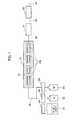
- Fig. 1 is a diagram illustrating a schematic configuration of the apparatus for manufacturing a heat-resistant composite material.
- This manufacturing apparatus constitutes a chemical vapor deposition (CVD) device or a chemical vapor infiltration (CVI) device and includes a horizontal hot-wall furnace 11 as a reaction furnace.
- the hot-wall furnace 11 is maintained at a predetermined temperature and a predetermined pressure and is supplied with a gas mixture including methyltrichlorosilane (CH 3 SiCl 3 : MTS) as a raw material gas, hydrogen (H 2 ) as a carrier gas, and hydrochloride (HCl) as an additive gas.
- a gas mixture including methyltrichlorosilane (CH 3 SiCl 3 : MTS) as a raw material gas, hydrogen (H 2 ) as a carrier gas, and hydrochloride (HCl) as an additive gas.
- CH 3 SiCl 3 methyltrichlorosilane
- H 2 hydrogen
- HCl hydrochloride
- a first flow channel 41 which supplies the gas mixture from the upstream side to the hot-wall furnace 11, is supplied with MTS as the raw material gas through a raw material gas flow rate controller 24 at a predetermined flow rate.
- MTS is stored in a raw material gas supply source 21 in the form of liquid, and a necessary amount of MTS is gasified and provided.
- the first flow channel 41 is supplied with hydrogen as the carrier gas from a carrier gas supply source 22 through a carrier gas flow rate controller 25 at a predetermined flow rate, and the first flow channel 41 is supplied with hydrochloride as the additive gas from an additive gas supply source 23 through an additive gas flow rate controller 26 at a predetermined flow rate.
- the raw material gas, carrier gas, and additive gas flow rate controllers 24, 25, and 26 are configured to control the flow rates of the raw material gas, carrier gas, and additive gas supplied to the first flow channel 41 into predetermined flow rates, respectively and each can be composed of an automatic valve, for example.
- the hot-wall furnace 11 includes a quartz tube 12.
- the gas mixture including the raw-material gas, carrier gas, and additive gas supplied from the first flow channel 41 is flown from one of the openings of the quartz tube 12 on the upstream side toward the other opening on the downstream side.
- the hot-wall furnace includes a not shown heating portion, which maintains a predetermined distribution of temperature within the hot-wall furnace 11.
- the hot-wall furnace 11 accommodates plural preforms 100, which are arranged side by side in the direction from the upstream side to the downstream side in the quartz tube 12.
- the preforms 100 are supplied with the gas mixture of the raw material gas, carrier gas, and additive gas at a predetermined temperature and a predetermined pressure, and silicon carbide (SiC) is deposited on the microstructures of the preforms 100 for film formation.
- exhaust gas containing the gas mixture not contributing the film formation of silicon carbide and byproducts concerning the film formation of silicon carbide is discharged to a second flow channel 42.
- the second flow channel 42 is connected to an automatic valve, which maintains a predetermined pressure within the quartz tube 12 of the hot-wall furnace 11.
- the automatic valve 31 is connected to a rotary pump 32 through a third flow channel 43.
- the rotary pump 32 is configured to discharge the exhaust gas supplied from the third flow channel 43 to a fourth flow channel 44 while providing a predetermined back pressure to the automatic valve 31.
- This manufacturing apparatus includes a not-shown controller.
- the controller controls the raw material gas, carrier gas, and additive gas flow rate controllers 24 to 26 to control the flow rates of the raw material gas, carrier gas, and additive gas supplied through the first flow channel 41 to the hot-wall furnace 11.
- the controller detects the temperature within the hot-wall furnace 11 using a not-shown thermocouple provided for the hot-wall furnace 11 and controls a not-shown heating portion to maintain the predetermined temperature within the hot-wall furnace 11.
- the controller controls the automatic valve 31 to make a control to maintain the predetermined pressure within the quartz tube 12 of the hot-wall furnace 11.
- the controller controls the flow rates of the raw material gas, carrier gas, and additive gas supplied to the hot-wall furnace 11 to control deposition of silicon carbide on the microstructures of the preforms 100 accommodated in the hot-wall furnace 11. For example, it is possible to set the flow rates of the raw material gas, carrier gas, and additive gas and the ratio of the flow rates thereof and set the amounts of additive gas added to the raw material and carrier gas.
- the controller performs the above-described control to support high growth rate of film formed on the microstructures of the preforms 100 and good filling uniformity at film formation at the same time.
- the controller ensures through the predetermined growth rate, the mass-productivity of the heat-resistant composite substance composed of the preform 100 impregnated with silicon carbide and, guarantees through the predetermined filling uniformity, the filling of silicon carbide in the microstructure of the preform 100.
- the deposition of silicon carbide on the microstructure of the preform 100 follows a first-order reaction mechanism or a reaction mechanism based on the Langmuir-Hinshelwood rate formula depending on the film forming species to be formed into a film.
- the control method varies depending on the reaction mechanisms, and the reaction mechanisms are individually described below.
- the controller makes a control to generate a large amount of film forming species having a low sticking probability.
- the species having a low sticking probability uniformly stick to the microstructure of preforms, ensuring the filling uniformity at film formation.
- the generation of a large amount of species ensures the growth rate at film formation. Accordingly, it is possible to ensure the compatibility between high growth rate and good filling uniformity.
- the controller controls the raw material gas, carrier gas, and additive gas flow rate controllers 24 to 26 so that the ratio between the flow rates of the raw material gas, carrier gas, and additive gas is set to a predetermined ratio.
- the controller makes a control so that only a predetermined amount of the additive gas is added to the raw material gas and carrier gas.
- the controller controls the raw material gas, carrier gas, and additive gas flow rate controllers 24 to 26 to adjust the flow rates of the raw material gas, carrier gas, and additive gas to predetermined flow rates.
- the controller controls parameters, including the ratio and flow rates of the raw material gas, carrier gas, and additive gas, to optimize the growth rate and filling uniformity.
- the growth rate at film formation is saturated with respect to the concentration as the concentration of the film forming species increases, and there is a zero-order reaction area where the growth rate does not depend on the concentration of the film-forming species.
- the controller makes a control to increase the concentration of the film-forming species to a high concentration not less than a predetermined value so that the concentration of the film-forming species falls in the zero-order reaction area.
- the growth rate at film formation is constant independently of the concentration, ensuring the filling uniformity at film formation.
- the increase in the concentration increases the growth rate. Accordingly, it is possible to ensure the compatibility between high growth rate and good filling uniformity.
- the controller controls the raw material gas, carrier gas, and additive gas flow rate controllers 24 to 26 so that the flow rates of the raw material gas, carrier gas, and additive gas are at a predetermined ratio. In other words, the controller allows only a predetermined amount of additive gas to be added to the raw material gas and carrier gas. Moreover, in order for the concentration of the film-forming species to fall in the zero-order region, the controller controls the raw material gas, carrier gas, and additive gas flow rate controllers 24 to 26 so that the flow rates of the raw material gas, carrier gas, and additive gas are adjusted to predetermined flow rates. Furthermore, the controller controls the parameters, including the ratio and flow rates of the raw material gas, carrier gas, and additive gas, to optimize the growth rate and filling uniformity.
- the additive gas containing chlorine has an etching effect, and the effect of etching silicon carbide to be deposited on the microstructure of the preforms 100 is higher in the upstream side where the additive gas is supplied to the quartz tube 12.
- the etching effect can prevent the microstructure from being clogged at film formation, thus ensuring good filling uniformity at film formation.
- the hot-wall furnace 11 which is as long as about several meters, for example, is provided and accommodates the plural preforms 100 which are arranged side by side from upstream to downstream in the quartz tube 12. Film of silicon carbide is simultaneously formed on the preforms 100.
- the controller reduces the growth rate in the upstream side of the quartz tube 12 so that the film formation rate is equal at the plural preforms 100.
- the controller controls the raw material gas, carrier gas, and additive gas flow rate controllers 24 to 26 and controls the not-shown heating portion to adjust the flow rate of the gas mixture and the distribution of temperature so that the concentration of the film-forming species is low in the upstream and high in the downstream.
- the controller makes a control so that the raw-material gas is sufficiently supplied to the downstream.
- the controller controls the raw material gas, carrier gas, and additive gas flow rate controllers 24 to 26 so that a sufficient flow rate of gas mixture is supplied.
- the gas mixture can be supplied not only from one end in the upstream of the quartz tube 12 but also simultaneously from another supply portion provided between the upstream end and the other end in the downstream of the quartz tube 12.
- the controller moreover makes a control to equalize the film formation rate from upstream to downstream and increase the use efficiency of the raw material gas in the supplied gas mixture.
- the controller can increase the use efficiency of the raw-material gas by properly controlling the parameters, including: the ratio, flow rates, and ways of supply of the raw-material gas, carrier gas, and additive gas supplied to the hot-wall furnace 11; and distributions of temperature and pressure in the hot-wall furnace 11. It is therefore possible to improve the distribution of film formation rate in the hot-wall furnace 11 and reduce the production cost.
- the controller can optimize the use efficiency of the raw-material gas.
- the controller used the embodiment can be easily implemented by using a commercially-available micro-controller configured to execute predetermined instructions.
- the controller can be implemented by executing a predetermined program with a general-purpose personal computer.
- the raw material gas, carrier gas, and additive gas are MTS, hydrogen, and chloride gas, respectively.
- the raw-material gas is not limited to MTS but can contain dimethyldichlorosilane (C 2 H 6 Cl 2 Si: DDS), trimethylchlorosilane (C 3 H 9 SiCl), silicon tetrachloride (SiCl 4 ), silane (SiH 4 ), propane (C 3 H 8 ), or the like.
- the carrier gas is not limited to hydrogen (H 2 ) and may also include noble gas such as nitrogen (N 2 ), helium (He), or argon (Ar).
- the additive gas is not limited to hydrochloride (HCl) and can also include molecules containing chlorine.
- Examples of the additive gas are: chlorine (Cl 2 ), methyl chloride (CH 3 Cl), dichloromethane (CH 2 Cl 2 ), chloroform (CHCl 3 ), carbon tetrachloride (CCl 4 ), vinyl chloride (C 2 H 3 Cl), benzene chloride (C 6 H 5 Cl), silicon tetrachloride (SiCl 4 ), trichlorosilane (SiHCl 3 ), dichlorosilane (SiH 2 Cl 2 ), dichloroethylene (C 2 H 2 Cl 2 ), tetrachloroethane (C 2 H 2 Cl 4 ), trichloroethane (C 2 H 3 Cl 3 ), and dichloroethane (C 2 H 4 Cl 2 ).
- the aforementioned molecules containing chlorine can provide molecules containing chlorine, which are adsorbed on the surface of the microstructure of the preforms 100.
- the molecules containing chlorine adsorbed on the surface of the microstructure lower the probability of sticking of the film-forming species to the microstructure. Accordingly, the filling uniformity at film formation can be ensured.
- the additive gas can include acetylene (C 2 H 2 ).
- the additive gas may be gas generating acetylene.
- the additive gas can include at least one of methane (CH 4 ), ethane (C 2 H 6 ), ethylene (C 2 H 4 ), methyl chloride (CH 3 Cl), dichloromethane (CH 2 Cl 2 ), chloroform (CHCl 3 ), carbon tetrachloride (CCl 4 ), vinyl chloride (C 2 H 3 Cl), benzene chloride (C 6 H 5 Cl), tetrachloroethane (C 2 H 2 Cl 4 ), trichloroethane (C 2 H 3 Cl 3 ), and dichloroethane (C 2 H 4 Cl 2 ).
- Silicon carbide as the film forming species of the first embodiment is generated through a process in which methyltrichlorosilane (MTS) as the raw-material gas is thermally decomposed; and the intermediates of molecules containing carbon and molecules containing silicon are adsorbed on the surface for association and reaction.
- MTS methyltrichlorosilane
- acetylene which is one of molecules containing carbon, has a comparatively inactive structure and has a low sticking probability (10 -3 ). Accordingly, by employing acetylene, the total sticking probability is reduced to ensure the filling uniformity, and supply of the film-forming species is accelerated to ensure high growth rate.
- the additive gas may include molecules containing carbon having a comparatively inactive structure similarly to acetylene (C 2 H 2 ).
- the additive gas can include at least one of methane (CH 4 ), ethane (C 2 H 6 ), and ethylene (C 2 H 4 ).
- the base material having the microstructure on which silicon carbide is deposited to form a film is the preform 100 of ceramic fibers but is not limited thereto.
- the base material can be composed of a preform of carbon fibers, a substrate provided with trenches in the surface, or porous ceramics.
- Example 1 the aforementioned manufacturing apparatus is used, and the quartz tube 12 provided for the hot-wall furnace 11 is used.
- the quartz tube 12 accommodates a Si (100) substrate with trenches formed in the surface as the base material having a microstructure.
- the actually-measured aspect ratio of the trenches is 10.9 on average.
- silicon carbide is deposited by chemical vapor deposition (CVD) or chemical vapor infiltration (CVI) for film formation.
- CVD chemical vapor deposition
- CVI chemical vapor infiltration
- the environment in the quartz tube 12 is maintained at a constant temperature of 1000°C and a constant pressure of 20 Torr.
- the gas mixture supplied to the quartz tube 12 includes MTS as the raw-material gas, hydrogen (H 2 ) and helium (He) as the carrier gas, and hydrochloride (HCl) as the additive gas.
- H 2 hydrogen
- He helium
- HCl hydrochloride
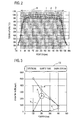
- Fig. 2 is a diagram showing the distribution of temperature in the hot-wall furnace 11.
- the hot-wall furnace 11 is provided with a 500 mm long heater extending in the longitudinal direction of the quartz tube 12 as the heating portion.
- the heater is movable between 0 mm at the inlet and 540 mm at the outlet along the quartz tube 12.
- the region between the inlet and outlet is indicated by a region R.
- the temperature within the hot-wall furnace 11 can be controlled by the not-shown controller.
- Polygonal lines 1 to 3 of Fig. 2 represent really-measured results of temperature when the temperature of the hot-wall furnace 11 is set by the controller to 900, 950, and 1000°C, respectively.
- the temperature is set by using thermocouples provided along the quartz tube 12. As shown in Fig. 2 , the set temperature is achieved with high accuracy in most of the region R, where the heater is movable, excepting portions in the inlet and outlet sides.
- Fig. 3 is a diagram showing the distribution of growth rate at film formation in the hot-wall furnace 11.
- the horizontal axis of Fig. 3 gives a location in the quartz tube 12, which is provided in the hot-wall furnace 11, in the direction from upstream to downstream of the flow of the gas mixture. The same applies to Figs. 4 to 6 below.
- the vertical axis in Fig. 3 gives the growth rate at film formation of silicon carbide.
- Polygonal lines a, b, and c in Fig. 3 respectively correspond to the samples A, B, and C which vary in the amount of hydrochloride as the additive gas added in the gas mixture.
- the sample A does not contain the additive gas.
- the sample B contains a small amount of hydrochloride, and the relative flow rate thereof is 0.5.
- the sample C contains a large amount of hydrochloride, and the relative flow rate thereof is 1.0. The same goes in Figs. 4 to 6 below.
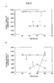
- Fig. 4 includes diagrams showing distributions of step coverage and sticking probability in the hot-wall furnace 11.
- the step coverage represents the filling uniformity at film formation and is given by a ratio of Tb/Tt where Tb and Tt are film thicknesses at the top opening and at the bottom in a trench constituting the microstructure as illustrated in Fig. 4(a) .
- the step coverage increases as hydrochloride as the additive gas increases while increasing towards the upstream side where a larger amount of hydrochloride is expected to be adsorbed.
- Figs. 3 and 4(a) show the followings: the growth rate is high at a point p of the polygonal line b in Fig. 3 , that is, at 200 mm in the case of the sample B, and at the point p of Fig. 4(a) , the step coverage is high, that is, high filling uniformity is implemented. In other words, high growth rate and good filling uniformity are supported at the same time under the conditions of the point p.
- Fig. 4(b) shows the sticking probability calculated from the step coverage.
- the calculation is performed by assuming that one type of film forming species is included for good vision. As a result, it is found that the sticking probability can reach the order of 10 -4 by introducing hydrochloride of the additive gas.
- Fig. 5 includes diagrams showing specific examples of the sticking probability.
- Fig. 5(a) shows the result for a first film-forming species
- Fig. 5(b) shows the result for a second film-forming species.
- the polygonal line a to be the highest, followed in order by the polygonal lines b and c. It is therefore found that the introduction of hydrochloride can lower the sticking probability.
- the polygonal line b corresponding to the relative flow rate of hydrochloride of 0.5 and the polygonal line c corresponding to the relative follow rate of hydrochloride of 1.0 reach an sticking probability of 0.001 which corresponds to the limit of the aspect ratio of the trench.
- Fig. 6 includes diagrams showing specific examples of contribution.
- the contribution is substantially constant at nearly 1 irrespective of whether hydrochloride is introduced.
- the contribution is smaller than 1 and depends on whether hydrochloride is introduced.
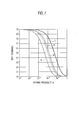
- Fig. 7 is a diagram showing the dependences of the step coverage on the aspect ratio and sticking probability.
- Curves 1 to 4 in Fig. 7 correspond to aspect ratios 4.7, 9.1, 10.7, and 16.5, respectively.
- the sticking probability can be set in an analyzable range of 10 -4 to 1.0.
- the aspect ratios can be used to classify plural film-forming species having different sticking probabilities.
- Example 2 the additive gas is methyl chloride (CH 3 Cl), and experiments are performed with three types of gas mixture: samples D, E, and F as shown in Table 2.
- the environment within the quartz tube 12 has a temperature of 1000°C.
- the other conditions are the same as those of Example 1.
- Lines d, e, and f in Table 2 represent the corresponding relations with data in Fig. 8 described later.
- the other components are shown in terms of relative flow rates.
- Fig. 8(a) is a diagram showing the distribution of growth rate at film formation in the hot-wall furnace 11
- Fig. 8(b) is a diagram showing the distribution of sticking probability in the hot-wall furnace 11.
- Polygonal lines d, e, and f in Figs. 8(a) and 8(b) correspond to the samples D, E, and F which vary in the amount of methyl chloride as the additive gas added in the gas mixture as shown in Table 2.
- the sample D does not contain the additive gas.
- the sample E contains a small amount of methyl chloride, and the relative flow rate thereof is 8.1 ⁇ 10 -3 .
- the sample C contains a large amount of methyl chloride, and the relative flow rate thereof is 4.0 ⁇ 10 -2 .
- Example 3 the additive gas is acetylene (C 2 H 2 ), and experiments are performed with four types of gas mixture in Table 3.
- Ref indicates a sample with the concentration of acetylene set to 0 for comparison.
- Polygonal lines g, h, i, and Ref in Table 3 represent the corresponding relations with data in Fig. 9 described later.
- Example 2 the environment within the quartz tube 12 is set to a temperature of 1000°C.
- the other conditions are the same as those of Example 1.
- Table 3 He (ARBITRARY UNIT) H 2 (ARBITRARY UNIT) C 2 H 2 (ARBITRARY UNIT) POLYGONAL LINE G 8.2 3.0 2.4 ⁇ 10 -2 g H 8.1 3.0 1.3 ⁇ 10 -1 h I 7.7 3.0 4.9 ⁇ 10 -1 i Ref 8.2 3.0 0.0 ref
- the relative flow rate of acetylene to MTS does not exceed 4.9 ⁇ 10 -1 .
- the optimal relative flow rate depends on the absolute pressure of MTS. The optimal relative flow rate needs to be set at each condition.
- Example 4 the additive gas is methane (CH 4 ), and experiments are performed with three types of gas mixture in Table 3.
- Ref indicates a sample with the concentration of methane set to 0 for comparison.
- Polygonal lines j, k, and Ref in Table 4 represent the corresponding relations with data in Fig. 10 described later.
- the present invention is applicable to manufacturing of heat-resistant composite materials and manufacturing of mechanical parts, high-temperature resistant semiconductors, and high voltage-resistant power devices including the heat-resistant composite materials.
Landscapes
- Chemical & Material Sciences (AREA)
- General Chemical & Material Sciences (AREA)
- Chemical Kinetics & Catalysis (AREA)
- Engineering & Computer Science (AREA)
- Materials Engineering (AREA)
- Mechanical Engineering (AREA)
- Metallurgy (AREA)
- Organic Chemistry (AREA)
- Inorganic Chemistry (AREA)
- Chemical Vapour Deposition (AREA)
Abstract
Description
- The present invention relates to a method and an apparatus for manufacturing a heat-resistant composite material containing silicon carbide.
- Silicon carbide (SiC) has a high breakdown voltage and is expected as a next-generation material of power semiconductors. Moreover, silicon carbide transmits visible light, and the coefficient of thermal expansion and lattice constant thereof are close to those of gallium nitride (GaN) Accordingly, silicon carbide is widely used for substrates of GaN-based LEDs and is a promising material used for semiconductor devices and ceramics.
- Such silicon carbide has excellent heat resistance and is expected to be applied to mechanical parts used at high temperature and the like. Those applications often require high mechanical strength, and silicon carbide is infiltrated into a preform made of ceramic fibers to be provided as a heat-resistant composite material with the toughness increased.
- The aforementioned heat-resistant composite materials are manufactured by depositing silicon carbide on the microstructure of preforms accommodated in a reactor often by chemical vapor deposition (CVD) or chemical vapor infiltration (CVI). There are two options for the material gas of silicon carbide including: a mixture of silane (SiH4) gas and hydrocarbon gas; and an organic silicon compound such as methyl trichlorosilane (CH3SiCl3: MTS).
-
- PTL1: Japanese Unexamined Patent Application Publication (Translation of PCT Application) No.
2001-508388 - PTL2: Japanese Patent Publication No.
3380761 -
- NPTL 1: Yasuyuki Fukusima, Kozue Hododuka, and Yukihiro Shimogaki, Multiscale analysis of SiC-CVD Process Reaction Mechanism, SCEJ 43rd Autumn Meeting (Nagoya Institute of Technology, 2011)
- NPTL 2: Yasuyuki Fukusima, Yuichi Funato, Kozue Hododuka, Ken Momose, and Yukihiro Shimogaki, Multiscale analysis (2) of SiC-CVD Process Reaction Mechanism, SCEJ 77th Annual Meeting (Kogakuin University, 2012)
- NPTL 3: F. Loumagne et al., J. Crystal Growth, 155(1995), 205
- NPTL 4: Yingbin Ge, Mark S. Gordon, Francine Battaglia, and Rodney O. Fox, J. Phys. Chem., 114(2010), 2384
- However, if the growth rate at which film of silicon carbide is formed on the microstructure of preforms is increased, the silicon carbide filling uniformity in the microstructure is degraded. On the other hand, if sufficient filling uniformity of silicon carbide is ensured, the growth rate is reduced. It is thus difficult to support high growth rate and good filling uniformity of silicon carbide at the same time.
- In the process of manufacturing the heat-resistant composite material in an industrial scale, plural preforms are placed in a long reactor, and film of silicon carbide is simultaneously formed on each preform. In this case, the film formation rate is not uniform from upstream to downstream of the flow of the raw material gas in the reactor.
- The present invention is made to solve the aforementioned problem, and an object of the invention is to provide a method and an apparatus for manufacturing a heat-resistant composite material which are capable of ensuring compatibility between high growth rate at which film of silicon carbide is formed on the microstructure and good filling uniformity of silicon carbide.
- Another object of the present invention is to provide a method and an apparatus for manufacturing a heat-resistant composite material which are capable of forming film on plural base materials which are placed in a reactor at uniform growth rate irrespective of the position of each base material.
- In order to solve the aforementioned problems, a method of manufacturing a heat-resistant composite material according to the application uses chemical vapor deposition or chemical vapor infiltration to cause raw material gas and carrier gas to flow in a reaction furnace accommodating a base material having a microstructure and to deposit silicon carbide on the base material for film formation. The method includes: adding additive gas to the raw material gas and carrier gas; and adjusting the amount of the added additive gas to control growth rate and filling uniformity at film formation of silicon carbide. Preferably, the reaction furnace is a hot-wall furnace.
- Preferably, the film formation of silicon carbide follows a first-order reaction, and the growth rate and filling uniformity at the film formation of silicon carbide are controlled by adjusting the amount of the added additive gas to control sticking probability of a film-forming species to the base material. Preferably, the growth rate and filling uniformity at the film formation of silicon carbide are optimized.
- Preferably, the film formation of silicon carbide follows a Langmuir-Hinshelwood rate formula, and the growth rate and filling uniformity at the film formation of silicon carbide are controlled by adjusting the amount of the additive gas added to make a control so that a zero-order reaction region of the Langmuir-Hinshelwood rate formula is used. Preferably, the growth rate and filling uniformity at the film formation of silicon carbide are optimized.
- Preferably, the amount of the additive gas added is used to control the distribution of growth rate at the film formation of silicon carbide with respect to the position in the reaction furnace. Preferably, the distribution of growth rate is optimized to be uniform.
- Preferably, the raw material gas is supplied through a plurality of positions located from upstream to downstream in the reaction furnace.
- Preferably, the raw material gas includes at least one of methyltrichlorosilane, dimethyldichlorosilane, trimethylchlorosilane, silicon tetrachloride, silane, and propane. Preferably, the carrier gas includes at least one of hydrogen, nitrogen, helium, and argon.
- Preferably, the additive gas includes molecules containing chlorine. Preferably, the additive gas includes at least one of hydrochloride, chlorine, methane chloride, dichloromethane, chloroform, carbon tetrachloride, vinyl chloride, benzene chloride, silicon tetrachloride, trichlorosilane, dichlorosilane, dichloroethylene, tetrachloroethane, trichloroethane, and dichloroethane.
- Preferably, the additive gas includes at least one of methane, ethane, ethylene, and acetylene.
- Preferably, the base material includes at least one of a preform of fibers, a substrate provided with a trench, and a porous substrate.
- A heat-resistant composite material manufacturing apparatus according to the application which uses chemical vapor deposition or chemical vapor infiltration to deposit silicon carbide on a base material having a microstructure for film formation, the method includes: a reaction furnace accommodating the base material; a raw material gas supply source supplying raw material gas to the reaction furnace; a carrier gas supply source supplying carrier gas to the reaction furnace; an additive gas supply source supplying additive gas to the reaction furnace; and a controller controlling an amount of the additive gas supplied. The controller uses the amount of the added additive gas to control growth rate and filling uniformity at the film formation of silicon carbide. Preferably, the reactive furnace is a hot-wall furnace.
- Preferably, the film formation of silicon carbide follows a first-order reaction, and the growth rate and filling uniformity at the film formation of silicon carbide are controlled by adjusting the amount of the added additive gas to control sticking probability of a film-forming species to the base material. Preferably, the controller optimizes the growth rate and filling uniformity at the film formation of silicon carbide.
- Preferably, the film formation of silicon carbide follows a Langmuir-Hinshelwood rate formula, and the controller controls growth rate and filling uniformity at the film formation of silicon carbide by adjusting the amount of the added additive gas to make a control so that a zero-order reaction region of the Langmuir-Hinshelwood rate formula is used. Preferably, the controller optimizes the growth rate and filling uniformity at the film formation of silicon carbide.
- Preferably, the controller uses the amount of the added additive gas to control the distribution of growth rate at the film formation of silicon carbide with respect to the position in the reaction furnace. Preferably, the distribution of growth rate is optimized to be uniform.
- Preferably, the apparatus includes a supply path to supply the raw material gas through a plurality of positions located from upstream to downstream in the reaction furnace.
- Preferably, the raw material gas includes at least one of methyltrichlorosilane, dimethyldichlorosilane, trimethylchlorosilane, silicon tetrachloride, silane, and propane. Preferably, the carrier gas includes at least one of hydrogen, nitrogen, helium, and argon.
- Preferably, the additive gas includes molecules containing chlorine. Preferably, the additive gas includes at least one of hydrochloride, chlorine, methane chloride, dichloromethane, chloroform, carbon tetrachloride, vinyl chloride, benzene chloride, silicon tetrachloride, trichlorosilane, dichlorosilane, dichloroethylene, tetrachloroethane, trichloroethane, and dichloroethane.
- Preferably, the additive gas includes at least one of methane, ethane, ethylene, and acetylene.
- Preferably, the base material includes at least one of a preform of fibers, a substrate provided with a trench, and a porous substrate.
- Preferably, the apparatus further includes: a raw material gas supply amount controller controlling the amount of the raw material gas supplied from the raw material gas supply source; a carrier gas supply amount controller controlling the amount of the carrier gas supplied from the carrier gas supply source; and an additive gas supply amount controller controlling the amount of the additive gas supplied from the additive gas supply source.
- According to the present invention, it is possible to ensure the compatibility between high growth rate and good filling uniformity at film formation of silicon carbide on the microstructure. Moreover, even when plural base materials on which film of silicon carbide is to be formed are placed in a reactor, it is possible to equalize the growth rate of film formation irrespective of location.
-
-
Fig. 1 is a diagram illustrating a schematic configuration of an apparatus for manufacturing a heat-resistant composite material. -
Fig. 2 is a diagram showing a distribution of temperature in a hot-wall furnace. -
Fig. 3 is a diagram showing a distribution of growth rate in the hot-wall furnace. -
Fig. 4 includes diagrams showing distributions of step coverage and sticking probability in the hot-wall furnace. -
Fig. 5 is a diagram illustrating a concrete example of the sticking probability. -
Fig. 6 includes diagrams illustrating concrete examples of contribution. -
Fig. 7 is a diagram illustrating dependences of step coverage on the aspect ratio and sticking probability. -
Fig. 8 includes diagrams illustrating the distributions of growth rate and sticking probability in the hot-wall furnace, respectively. -
Fig. 9 includes diagrams respectively illustrating the distributions of growth rate and sticking probability when acetylene is added. -
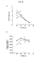
Fig. 10 includes diagrams respectively illustrating the distributions of growth rate and sticking probability when methane is added. - Hereinafter, a description is given of a method and an apparatus for manufacturing a heat-resistant composite material according to the present invention in detail with reference to the drawings.
-
Fig. 1 is a diagram illustrating a schematic configuration of the apparatus for manufacturing a heat-resistant composite material. This manufacturing apparatus constitutes a chemical vapor deposition (CVD) device or a chemical vapor infiltration (CVI) device and includes a horizontal hot-wall furnace 11 as a reaction furnace. The hot-wall furnace 11 is maintained at a predetermined temperature and a predetermined pressure and is supplied with a gas mixture including methyltrichlorosilane (CH3SiCl3: MTS) as a raw material gas, hydrogen (H2) as a carrier gas, and hydrochloride (HCl) as an additive gas. - A
first flow channel 41, which supplies the gas mixture from the upstream side to the hot-wall furnace 11, is supplied with MTS as the raw material gas through a raw material gasflow rate controller 24 at a predetermined flow rate. MTS is stored in a raw materialgas supply source 21 in the form of liquid, and a necessary amount of MTS is gasified and provided. In a similar manner, thefirst flow channel 41 is supplied with hydrogen as the carrier gas from a carriergas supply source 22 through a carrier gasflow rate controller 25 at a predetermined flow rate, and thefirst flow channel 41 is supplied with hydrochloride as the additive gas from an additivegas supply source 23 through an additive gasflow rate controller 26 at a predetermined flow rate. - The raw material gas, carrier gas, and additive gas
flow rate controllers first flow channel 41 into predetermined flow rates, respectively and each can be composed of an automatic valve, for example. - The hot-
wall furnace 11 includes aquartz tube 12. In the hot-wall furnace 11, the gas mixture including the raw-material gas, carrier gas, and additive gas supplied from thefirst flow channel 41 is flown from one of the openings of thequartz tube 12 on the upstream side toward the other opening on the downstream side. The hot-wall furnace includes a not shown heating portion, which maintains a predetermined distribution of temperature within the hot-wall furnace 11. - The hot-
wall furnace 11 accommodatesplural preforms 100, which are arranged side by side in the direction from the upstream side to the downstream side in thequartz tube 12. Thepreforms 100 are supplied with the gas mixture of the raw material gas, carrier gas, and additive gas at a predetermined temperature and a predetermined pressure, and silicon carbide (SiC) is deposited on the microstructures of thepreforms 100 for film formation. - From the opening of the
quartz tube 12 on the downstream side in the hot-wall furnace 11, exhaust gas containing the gas mixture not contributing the film formation of silicon carbide and byproducts concerning the film formation of silicon carbide is discharged to asecond flow channel 42. Thesecond flow channel 42 is connected to an automatic valve, which maintains a predetermined pressure within thequartz tube 12 of the hot-wall furnace 11. - The
automatic valve 31 is connected to arotary pump 32 through athird flow channel 43. Therotary pump 32 is configured to discharge the exhaust gas supplied from thethird flow channel 43 to afourth flow channel 44 while providing a predetermined back pressure to theautomatic valve 31. - This manufacturing apparatus includes a not-shown controller. The controller controls the raw material gas, carrier gas, and additive gas
flow rate controllers 24 to 26 to control the flow rates of the raw material gas, carrier gas, and additive gas supplied through thefirst flow channel 41 to the hot-wall furnace 11. - The controller detects the temperature within the hot-
wall furnace 11 using a not-shown thermocouple provided for the hot-wall furnace 11 and controls a not-shown heating portion to maintain the predetermined temperature within the hot-wall furnace 11. The controller controls theautomatic valve 31 to make a control to maintain the predetermined pressure within thequartz tube 12 of the hot-wall furnace 11. - In the first embodiment, the controller controls the flow rates of the raw material gas, carrier gas, and additive gas supplied to the hot-
wall furnace 11 to control deposition of silicon carbide on the microstructures of thepreforms 100 accommodated in the hot-wall furnace 11. For example, it is possible to set the flow rates of the raw material gas, carrier gas, and additive gas and the ratio of the flow rates thereof and set the amounts of additive gas added to the raw material and carrier gas. - The controller performs the above-described control to support high growth rate of film formed on the microstructures of the
preforms 100 and good filling uniformity at film formation at the same time. In other words, the controller ensures through the predetermined growth rate, the mass-productivity of the heat-resistant composite substance composed of thepreform 100 impregnated with silicon carbide and, guarantees through the predetermined filling uniformity, the filling of silicon carbide in the microstructure of thepreform 100. - Herein, the deposition of silicon carbide on the microstructure of the
preform 100 follows a first-order reaction mechanism or a reaction mechanism based on the Langmuir-Hinshelwood rate formula depending on the film forming species to be formed into a film. The control method varies depending on the reaction mechanisms, and the reaction mechanisms are individually described below. - When the film forming species of silicon carbide follows a first-order reaction mechanism, the growth rate at film formation of silicon carbide is in a first-order relation with the concentration of the film forming species. In this case, the controller makes a control to generate a large amount of film forming species having a low sticking probability. The species having a low sticking probability uniformly stick to the microstructure of preforms, ensuring the filling uniformity at film formation. Moreover, the generation of a large amount of species ensures the growth rate at film formation. Accordingly, it is possible to ensure the compatibility between high growth rate and good filling uniformity.
- In order to generate a film forming species having a low sticking probability, the controller controls the raw material gas, carrier gas, and additive gas
flow rate controllers 24 to 26 so that the ratio between the flow rates of the raw material gas, carrier gas, and additive gas is set to a predetermined ratio. In other words, the controller makes a control so that only a predetermined amount of the additive gas is added to the raw material gas and carrier gas. Moreover, in order to generate a large amount of film forming species, the controller controls the raw material gas, carrier gas, and additive gasflow rate controllers 24 to 26 to adjust the flow rates of the raw material gas, carrier gas, and additive gas to predetermined flow rates. Furthermore, the controller controls parameters, including the ratio and flow rates of the raw material gas, carrier gas, and additive gas, to optimize the growth rate and filling uniformity. - In the case where the film forming species of silicon carbide follows the reaction mechanism based on the Langmuir-Hinshelwood rate formula, the growth rate at film formation is saturated with respect to the concentration as the concentration of the film forming species increases, and there is a zero-order reaction area where the growth rate does not depend on the concentration of the film-forming species. The controller makes a control to increase the concentration of the film-forming species to a high concentration not less than a predetermined value so that the concentration of the film-forming species falls in the zero-order reaction area. In the zero-order reaction area of the film-forming species, the growth rate at film formation is constant independently of the concentration, ensuring the filling uniformity at film formation. Moreover, the increase in the concentration increases the growth rate. Accordingly, it is possible to ensure the compatibility between high growth rate and good filling uniformity.
- The controller controls the raw material gas, carrier gas, and additive gas
flow rate controllers 24 to 26 so that the flow rates of the raw material gas, carrier gas, and additive gas are at a predetermined ratio. In other words, the controller allows only a predetermined amount of additive gas to be added to the raw material gas and carrier gas. Moreover, in order for the concentration of the film-forming species to fall in the zero-order region, the controller controls the raw material gas, carrier gas, and additive gasflow rate controllers 24 to 26 so that the flow rates of the raw material gas, carrier gas, and additive gas are adjusted to predetermined flow rates. Furthermore, the controller controls the parameters, including the ratio and flow rates of the raw material gas, carrier gas, and additive gas, to optimize the growth rate and filling uniformity. - Irrespective of which reaction mechanism the film-forming species follow, the additive gas containing chlorine has an etching effect, and the effect of etching silicon carbide to be deposited on the microstructure of the
preforms 100 is higher in the upstream side where the additive gas is supplied to thequartz tube 12. The etching effect can prevent the microstructure from being clogged at film formation, thus ensuring good filling uniformity at film formation. - On the other hand, in some cases of manufacturing the heat-resistant composite material in an industrial scale, the hot-
wall furnace 11 which is as long as about several meters, for example, is provided and accommodates theplural preforms 100 which are arranged side by side from upstream to downstream in thequartz tube 12. Film of silicon carbide is simultaneously formed on thepreforms 100. - In the aforementioned case, the controller reduces the growth rate in the upstream side of the
quartz tube 12 so that the film formation rate is equal at theplural preforms 100. For example, the controller controls the raw material gas, carrier gas, and additive gasflow rate controllers 24 to 26 and controls the not-shown heating portion to adjust the flow rate of the gas mixture and the distribution of temperature so that the concentration of the film-forming species is low in the upstream and high in the downstream. - The controller makes a control so that the raw-material gas is sufficiently supplied to the downstream. For example, the controller controls the raw material gas, carrier gas, and additive gas
flow rate controllers 24 to 26 so that a sufficient flow rate of gas mixture is supplied. Moreover, the gas mixture can be supplied not only from one end in the upstream of thequartz tube 12 but also simultaneously from another supply portion provided between the upstream end and the other end in the downstream of thequartz tube 12. - The controller moreover makes a control to equalize the film formation rate from upstream to downstream and increase the use efficiency of the raw material gas in the supplied gas mixture. For example, the controller can increase the use efficiency of the raw-material gas by properly controlling the parameters, including: the ratio, flow rates, and ways of supply of the raw-material gas, carrier gas, and additive gas supplied to the hot-
wall furnace 11; and distributions of temperature and pressure in the hot-wall furnace 11. It is therefore possible to improve the distribution of film formation rate in the hot-wall furnace 11 and reduce the production cost. Moreover, by using the aforementioned parameters, the controller can optimize the use efficiency of the raw-material gas. - The controller used the embodiment can be easily implemented by using a commercially-available micro-controller configured to execute predetermined instructions. Alternatively, the controller can be implemented by executing a predetermined program with a general-purpose personal computer.
- In the embodiment, the raw material gas, carrier gas, and additive gas are MTS, hydrogen, and chloride gas, respectively. However, the present invention is not limited to those. The raw-material gas is not limited to MTS but can contain dimethyldichlorosilane (C2H6Cl2Si: DDS), trimethylchlorosilane (C3H9SiCl), silicon tetrachloride (SiCl4), silane (SiH4), propane (C3H8), or the like. Moreover, the carrier gas is not limited to hydrogen (H2) and may also include noble gas such as nitrogen (N2), helium (He), or argon (Ar).
- The additive gas is not limited to hydrochloride (HCl) and can also include molecules containing chlorine. Examples of the additive gas are: chlorine (Cl2), methyl chloride (CH3Cl), dichloromethane (CH2Cl2), chloroform (CHCl3), carbon tetrachloride (CCl4), vinyl chloride (C2H3Cl), benzene chloride (C6H5Cl), silicon tetrachloride (SiCl4), trichlorosilane (SiHCl3), dichlorosilane (SiH2Cl2), dichloroethylene (C2H2Cl2), tetrachloroethane (C2H2Cl4), trichloroethane (C2H3Cl3), and dichloroethane (C2H4Cl2).
- The aforementioned molecules containing chlorine can provide molecules containing chlorine, which are adsorbed on the surface of the microstructure of the
preforms 100. The molecules containing chlorine adsorbed on the surface of the microstructure lower the probability of sticking of the film-forming species to the microstructure. Accordingly, the filling uniformity at film formation can be ensured. - The additive gas can include acetylene (C2H2). Alternatively, the additive gas may be gas generating acetylene. For example, the additive gas can include at least one of methane (CH4), ethane (C2H6), ethylene (C2H4), methyl chloride (CH3Cl), dichloromethane (CH2Cl2), chloroform (CHCl3), carbon tetrachloride (CCl4), vinyl chloride (C2H3Cl), benzene chloride (C6H5Cl), tetrachloroethane (C2H2Cl4), trichloroethane (C2H3Cl3), and dichloroethane (C2H4Cl2).
- Silicon carbide as the film forming species of the first embodiment is generated through a process in which methyltrichlorosilane (MTS) as the raw-material gas is thermally decomposed; and the intermediates of molecules containing carbon and molecules containing silicon are adsorbed on the surface for association and reaction. Herein, acetylene, which is one of molecules containing carbon, has a comparatively inactive structure and has a low sticking probability (10-3). Accordingly, by employing acetylene, the total sticking probability is reduced to ensure the filling uniformity, and supply of the film-forming species is accelerated to ensure high growth rate.
- The additive gas may include molecules containing carbon having a comparatively inactive structure similarly to acetylene (C2H2). For example, the additive gas can include at least one of methane (CH4), ethane (C2H6), and ethylene (C2H4).
- The base material having the microstructure on which silicon carbide is deposited to form a film is the
preform 100 of ceramic fibers but is not limited thereto. The base material can be composed of a preform of carbon fibers, a substrate provided with trenches in the surface, or porous ceramics. - In Example 1, the aforementioned manufacturing apparatus is used, and the
quartz tube 12 provided for the hot-wall furnace 11 is used. Thequartz tube 12 accommodates a Si (100) substrate with trenches formed in the surface as the base material having a microstructure. The actually-measured aspect ratio of the trenches is 10.9 on average. - On this substrate, silicon carbide is deposited by chemical vapor deposition (CVD) or chemical vapor infiltration (CVI) for film formation. As the growth conditions, the environment in the
quartz tube 12 is maintained at a constant temperature of 1000°C and a constant pressure of 20 Torr. The gas mixture supplied to thequartz tube 12 includes MTS as the raw-material gas, hydrogen (H2) and helium (He) as the carrier gas, and hydrochloride (HCl) as the additive gas. Experiments are performed with three types of gas mixture: samples A, B, and C as shown in Table 1 below. In Table 1, by using the flow rate of MTS as the reference, the other components are shown in terms of relative flow rates. Polygonal lines a, b, and c in Table 1 represent the corresponding relations with data inFigs. 3 to 6 described later.Table 1 He (ARBITRARY UNIT) H2 (ARBITRARY UNIT) HCL (ARBITRARY UNIT) POLYGONAL LINE A 9 2.5 0 a B 8.5 2.5 0.5 b C 8 2.5 1.0 c -
Fig. 2 is a diagram showing the distribution of temperature in the hot-wall furnace 11. The hot-wall furnace 11 is provided with a 500 mm long heater extending in the longitudinal direction of thequartz tube 12 as the heating portion. The heater is movable between 0 mm at the inlet and 540 mm at the outlet along thequartz tube 12. InFig. 2 , the region between the inlet and outlet is indicated by a region R. - The temperature within the hot-
wall furnace 11 can be controlled by the not-shown controller.Polygonal lines 1 to 3 ofFig. 2 represent really-measured results of temperature when the temperature of the hot-wall furnace 11 is set by the controller to 900, 950, and 1000°C, respectively. The temperature is set by using thermocouples provided along thequartz tube 12. As shown inFig. 2 , the set temperature is achieved with high accuracy in most of the region R, where the heater is movable, excepting portions in the inlet and outlet sides. -
Fig. 3 is a diagram showing the distribution of growth rate at film formation in the hot-wall furnace 11. The horizontal axis ofFig. 3 gives a location in thequartz tube 12, which is provided in the hot-wall furnace 11, in the direction from upstream to downstream of the flow of the gas mixture. The same applies toFigs. 4 to 6 below. The vertical axis inFig. 3 gives the growth rate at film formation of silicon carbide. - Polygonal lines a, b, and c in
Fig. 3 respectively correspond to the samples A, B, and C which vary in the amount of hydrochloride as the additive gas added in the gas mixture. The sample A does not contain the additive gas. The sample B contains a small amount of hydrochloride, and the relative flow rate thereof is 0.5. The sample C contains a large amount of hydrochloride, and the relative flow rate thereof is 1.0. The same goes inFigs. 4 to 6 below. - As apparent from
Fig. 3 , as the amount of hydrochloride added increases, the growth rate at film formation lowers, and the peak in the distribution of flow rate shifts downstream. This is considered to be because a large amount of hydrochloride is adsorbed to the base material and prevents film formation in the upstream. -
Fig. 4 includes diagrams showing distributions of step coverage and sticking probability in the hot-wall furnace 11. Herein, the step coverage represents the filling uniformity at film formation and is given by a ratio of Tb/Tt where Tb and Tt are film thicknesses at the top opening and at the bottom in a trench constituting the microstructure as illustrated inFig. 4(a) . As apparent fromFig. 4(a) , the step coverage increases as hydrochloride as the additive gas increases while increasing towards the upstream side where a larger amount of hydrochloride is expected to be adsorbed. - The comparison between
Figs. 3 and4(a) shows the followings: the growth rate is high at a point p of the polygonal line b inFig. 3 , that is, at 200 mm in the case of the sample B, and at the point p ofFig. 4(a) , the step coverage is high, that is, high filling uniformity is implemented. In other words, high growth rate and good filling uniformity are supported at the same time under the conditions of the point p. -
Fig. 4(b) shows the sticking probability calculated from the step coverage. Herein, the calculation is performed by assuming that one type of film forming species is included for good vision. As a result, it is found that the sticking probability can reach the order of 10-4 by introducing hydrochloride of the additive gas. -
Fig. 5 includes diagrams showing specific examples of the sticking probability.Fig. 5(a) shows the result for a first film-forming species, andFig. 5(b) shows the result for a second film-forming species. In terms of sticking probability of both the first and second film forming species, there is a tendency for the polygonal line a to be the highest, followed in order by the polygonal lines b and c. It is therefore found that the introduction of hydrochloride can lower the sticking probability. In the case of the first film-forming species, the polygonal line b corresponding to the relative flow rate of hydrochloride of 0.5 and the polygonal line c corresponding to the relative follow rate of hydrochloride of 1.0 reach an sticking probability of 0.001 which corresponds to the limit of the aspect ratio of the trench. -
Fig. 6 includes diagrams showing specific examples of contribution. As for the first film-forming species shown inFig. 6(a) , the contribution is substantially constant at nearly 1 irrespective of whether hydrochloride is introduced. On the other hand, as for the second film-forming species shown inFig. 6(b) , the contribution is smaller than 1 and depends on whether hydrochloride is introduced. -
Fig. 7 is a diagram showing the dependences of the step coverage on the aspect ratio and sticking probability.Curves 1 to 4 inFig. 7 correspond to aspect ratios 4.7, 9.1, 10.7, and 16.5, respectively. By using various aspect ratios, the sticking probability can be set in an analyzable range of 10-4 to 1.0. Simultaneously, the aspect ratios can be used to classify plural film-forming species having different sticking probabilities. - In Example 2, the additive gas is methyl chloride (CH3Cl), and experiments are performed with three types of gas mixture: samples D, E, and F as shown in Table 2. As the growth conditions, the environment within the
quartz tube 12 has a temperature of 1000°C. The other conditions are the same as those of Example 1. Lines d, e, and f in Table 2 represent the corresponding relations with data inFig. 8 described later. In table 2, by using the flow rate of MTS as the reference, the other components are shown in terms of relative flow rates.Table 2 He (ARBITRARY UNIT) H2 (ARBITRARY UNIT) CH3Cl (ARBITRARY UNIT) POLYGONAL LINE D 2.3 1.1 0 d E 2.3 1.1 8.1×10⁻³ e F 2.3 1.1 4.0×10⁻² f -
Fig. 8(a) is a diagram showing the distribution of growth rate at film formation in the hot-wall furnace 11, andFig. 8(b) is a diagram showing the distribution of sticking probability in the hot-wall furnace 11. Polygonal lines d, e, and f inFigs. 8(a) and 8(b) correspond to the samples D, E, and F which vary in the amount of methyl chloride as the additive gas added in the gas mixture as shown in Table 2. The sample D does not contain the additive gas. The sample E contains a small amount of methyl chloride, and the relative flow rate thereof is 8.1×10⁻³. The sample C contains a large amount of methyl chloride, and the relative flow rate thereof is 4.0×10⁻². - As apparent from
Figs. 8(a) and 8(b) , the experiment with the relative flow rate of methyl chloride of 8.1×10⁻³, which is represented by the polygonal line e, results in high growth rate of thin film and low sticking probability. The growth rate and sticking probability have very good values especially at the positions of 100 and 200 mm. This result reveals that both high growth rate and good filling uniformity at film formation of silicon carbide are implemented. - In Example 3, the additive gas is acetylene (C2H2), and experiments are performed with four types of gas mixture in Table 3. Herein, Ref indicates a sample with the concentration of acetylene set to 0 for comparison. Polygonal lines g, h, i, and Ref in Table 3 represent the corresponding relations with data in
Fig. 9 described later. - Similarly to Example 2, the environment within the
quartz tube 12 is set to a temperature of 1000°C. The other conditions are the same as those of Example 1. The same applies to the following example.Table 3 He (ARBITRARY UNIT) H2 (ARBITRARY UNIT) C2H2 (ARBITRARY UNIT) POLYGONAL LINE G 8.2 3.0 2.4×10⁻² g H 8.1 3.0 1.3×10⁻¹ h I 7.7 3.0 4.9×10⁻¹ i Ref 8.2 3.0 0.0 ref - As shown in
Fig. 9 , when acetylene is added, the effect of reducing the sticking probability and increasing the film-forming rate can be confirmed. - Preferably, the relative flow rate of acetylene to MTS does not exceed 4.9×10⁻¹. However, the optimal relative flow rate depends on the absolute pressure of MTS. The optimal relative flow rate needs to be set at each condition.
- In Example 4, the additive gas is methane (CH4), and experiments are performed with three types of gas mixture in Table 3. Herein, Ref indicates a sample with the concentration of methane set to 0 for comparison. Polygonal lines j, k, and Ref in Table 4 represent the corresponding relations with data in
Fig. 10 described later.Table 4 He (ARBITRARY UNIT) H2 (ARBITRARY UNIT) CH4 (ARBITRARY UNIT) POLYGONAL LINE J 8.0 3.0 1.8×10⁻¹ j K 7.6 3.0 5.4×10⁻¹ k Ref 8.2 3.0 0.0 ref - As shown in
Fig. 10 , the addition of methane is effective on increasing the film-forming rate without changing the sticking probability very much. - The embodiment and examples of the present invention described above show just examples to which the present invention is applied, and the present invention is not limited to those.
- The present invention is applicable to manufacturing of heat-resistant composite materials and manufacturing of mechanical parts, high-temperature resistant semiconductors, and high voltage-resistant power devices including the heat-resistant composite materials.
-
- 11
- HOT-WALL FURNACE
- 12
- QUARTZ TUBE
- 21
- RAW MATERIAL GAS SUPPLY SOURCE
- 22
- CARRIER GAS SUPPLY SOURCE
- 23
- ADDITIVE GAS SUPPLY SOURCE
- 24, 25, 26
- FLOW RATE CONTROLLER
- 31
- ROTARY PUMP
- 100
- PREFORM
Claims (35)
- A method of manufacturing a heat-resistant composite material which uses chemical vapor deposition or chemical vapor infiltration to causes raw material gas and carrier gas to flow in a reaction furnace accommodating a base material having a microstructure and deposit silicon carbide on the base material for film formation, the method comprising:adding additive gas to the raw material gas and carrier gas; andadjusting the amount of the added additive gas to control growth rate and filling uniformity at the film formation of silicon carbide.
- The method of manufacturing a heat-resistant composite material according to claim 1, wherein
the film formation of silicon carbide follows a first-order reaction, and the growth rate and filling uniformity at the film formation of silicon carbide are controlled by adjusting the amount of the added additive gas to control sticking probability of a film-forming species to the base material. - The method of manufacturing a heat-resistant composite material according to claim 1, wherein
the film formation of silicon carbide follows a Langmuir-Hinshelwood rate formula, and the growth rate and filling uniformity at the film formation of silicon carbide are controlled by adjusting the amount of the added additive gas to make a control so that a zero-order reaction region of the Langmuir-Hinshelwood rate formula is used. - The method of manufacturing a heat-resistant composite material according to claim 2 or 3, wherein the growth rate and filling uniformity at the film formation of silicon carbide are optimized.
- The method of manufacturing a heat-resistant composite material according to any one of claims 1 to 4, wherein the amount of the added additive gas is adjusted to control the distribution of growth rate at the film formation of silicon carbide with respect to the position in the reaction furnace.
- The method of manufacturing a heat-resistant composite material according to claim 5, wherein the distribution of growth rate is optimized to be uniform.
- The method of manufacturing a heat-resistant composite material according to claim 5 or 6, wherein the raw material gas is supplied through a plurality of positions located from upstream to downstream in the reaction furnace.
- The method of manufacturing a heat-resistant composite material according to any one of claims 1 to 7, wherein the raw material gas includes at least one of methyltrichlorosilane, dimethyldichlorosilane, trimethylchlorosilane, silicon tetrachloride, silane, and propane.
- The method of manufacturing a heat-resistant composite material according to any one of claims 1 to 8, wherein the carrier gas includes at least one of hydrogen, nitrogen, helium, and argon.
- The method of manufacturing a heat-resistant composite material according to any one of claims 1 to 9, wherein the additive gas includes molecules containing chlorine.
- The method of manufacturing a heat-resistant composite material according to any one of claim 10, wherein the additive gas includes at least one of hydrochloride, chlorine, methane chloride, dichloromethane, chloroform, carbon tetrachloride, vinyl chloride, benzene chloride, silicon tetrachloride, trichlorosilane, dichlorosilane, dichloroethylene, tetrachloroethane, trichloroethane, and dichloromethane.
- The method of manufacturing a heat-resistant composite material according to any one of claims 1 to 11, wherein the additive gas includes one of acetylene and gas which can generate acetylene through decomposition or reaction.
- The method of manufacturing a heat-resistant composite material according to claim 12, wherein the raw material gas is methyltrichlorosilane and the relative flow rate of acetylene to the flow rate of methyltrichlorosilane does not exceed 4.9×10⁻¹.
- The method of manufacturing a heat-resistant composite material according to any one of claims 1 to 13, wherein the additive gas includes at least one of methane, ethylene, and ethane.
- The method of manufacturing a heat-resistant composite material according to any one of claims 1 to 14, wherein the additive gas has an etching operation.
- The method of manufacturing a heat-resistant composite material according to any one of claims 1 to 15, wherein the base material includes at least one of a preform of fibers, a substrate provided with a trench, and a porous substrate.
- The method of manufacturing a heat-resistant composite material according to any one of claims 1 to 16, wherein the reaction furnace is a hot-wall furnace.
- A heat-resistant composite material manufacturing apparatus which uses chemical vapor deposition or chemical vapor infiltration to deposit silicon carbide on a base material having a microstructure for film formation, the apparatus comprising:a reaction furnace accommodating the base material;a raw material gas supply source supplying raw material gas to the reaction furnace;a carrier gas supply source supplying carrier gas to the reaction furnace;an additive gas supply source supplying additive gas to the reaction furnace; anda controller controlling an amount of the additive gas supplied, whereinthe controller uses the amount of the added additive gas to control growth rate and filling uniformity at the film formation of silicon carbide.
- The heat-resistant composite material manufacturing apparatus according to claim 18, wherein
the film formation of silicon carbide follows a first-order reaction, and the controller controls the growth rate and filling uniformity at the film formation of silicon carbide by adjusting the amount of the added additive gas to control sticking probability of a film-forming species to the base material. - The method of manufacturing a heat-resistant composite material according to claim 18, wherein
the film formation of silicon carbide follows a Langmuir-Hinshelwood rate formula, and the controller controls the growth rate and filling uniformity at the film formation of silicon carbide by adjusting the amount of the added additive gas to make a control so that a zero-order reaction region of the Langmuir-Hinshelwood rate formula is used. - The heat-resistan composite material manufacturing apparatus according to claim 19 or 20, wherein the controller optimizes the growth rate and filling uniformity at the film formation of silicon carbide.
- The heat-resistant composite material manufacturing apparatus according to any one of claims 18 to 21, wherein the controller uses the amount of the additive gas added to control the distribution of growth rate at the film formation of silicon carbide with respect to the position in the reaction furnace.
- The heat-resistant composite material manufacturing apparatus according to claim 22, wherein the distribution of growth rate is optimized to be uniform.
- The heat-resistant composite material manufacturing apparatus according to claim 22 or 23, further comprising a supply path to supply the raw material gas from a plurality of positions located from upstream to downstream in the reaction furnace.
- The heat-resistant composite material manufacturing apparatus according to any one of claims 18 to 24, wherein the raw material gas includes at least one of methyltrichlorosilane, dimethyldichlorosilane, trimethylchlorosilane, silicon tetrachloride, silane, and propane.
- The heat-resistant composite material manufacturing apparatus according to any one of claims 18 to 25, wherein the carrier gas includes at least one of hydrogen, nitrogen, helium, and argon.
- The heat-resistant composite material manufacturing apparatus according to any one of claims 18 to 26, wherein the additive gas includes molecules containing chlorine.
- The heat-resistant composite material manufacturing apparatus according to any one of claim 27, wherein the additive gas includes at least one of hydrochloride, chlorine, methane chloride, dichloromethane, chloroform, carbon tetrachloride, vinyl chloride, benzene chloride, silicon tetrachloride, trichlorosilane, dichlorosilane, dichloroethylene, tetrachloroethane, trichloroethane, and dichloromethane.
- The heat-resistant composite material manufacturing apparatus according to any one of claims 18 to 28, wherein the additive gas includes one of acetylene and gas which can generate acetylene through decomposition or reaction.
- The heat-resistant composite material manufacturing apparatus according to claim 29, wherein the raw material gas is methyltrichlorosilane and the relative flow rate of acetylene to the flow rate of methyltrichlorosilane does not exceed 4.9×10⁻¹.
- The method of manufacturing a heat-resistant composite material according to any one of claims 18 to 30, wherein the additive gas includes at least one of methane, ethylene, and ethane.
- The heat-resistant composite material manufacturing apparatus according to any one of claims 18 to 31, wherein the additive gas has an etching operation.
- The heat-resistant composite material manufacturing apparatus according to any one of claims 18 to 32, wherein the base material includes at least one of a preform of fibers, a substrate provided with a trench, and a porous substrate.
- The heat-resistant composite material manufacturing apparatus according to any one of claims 18 to 33, further comprising:a raw material gas supply amount controller controlling the amount of the raw material gas supplied from the raw material gas supply source;a carrier gas supply amount controller controlling the amount of the carrier gas supplied from the carrier gas supply source; andan additive gas supply amount controller controlling the amount of the additive gas supplied from the additive gas supply source.
- The heat-resistant composite material manufacturing apparatus according to any one of claims 18 to 34, wherein the reaction furnace is a hot-wall furnace.
Applications Claiming Priority (2)
| Application Number | Priority Date | Filing Date | Title |
|---|---|---|---|
| JP2012181016 | 2012-08-17 | ||
| PCT/JP2013/053749 WO2014027472A1 (en) | 2012-08-17 | 2013-02-15 | Method for manufacturing heat resistant composite material and manufacturing device |
Publications (2)
| Publication Number | Publication Date |
|---|---|
| EP2896718A1 true EP2896718A1 (en) | 2015-07-22 |
| EP2896718A4 EP2896718A4 (en) | 2016-04-06 |
Family
ID=50685513
Family Applications (1)
| Application Number | Title | Priority Date | Filing Date |
|---|---|---|---|
| EP13879446.6A Withdrawn EP2896718A4 (en) | 2012-08-17 | 2013-02-15 | METHOD FOR MANUFACTURING HEAT-RESISTANT COMPOSITE MATERIAL AND DEVICE FOR MANUFACTURING |
Country Status (5)
| Country | Link |
|---|---|
| US (1) | US9822445B2 (en) |
| EP (1) | EP2896718A4 (en) |
| JP (1) | JP5906318B2 (en) |
| CN (1) | CN104619881A (en) |
| WO (1) | WO2014027472A1 (en) |
Cited By (2)
| Publication number | Priority date | Publication date | Assignee | Title |
|---|---|---|---|---|
| US11718569B2 (en) | 2018-06-01 | 2023-08-08 | Ihi Corporation | Production method for composite material |
| WO2023194483A1 (en) * | 2022-04-06 | 2023-10-12 | Sgl Carbon Se | Substrate comprising conformal metal carbide coating |
Families Citing this family (321)
| Publication number | Priority date | Publication date | Assignee | Title |
|---|---|---|---|---|
| US9394608B2 (en) | 2009-04-06 | 2016-07-19 | Asm America, Inc. | Semiconductor processing reactor and components thereof |
| US8802201B2 (en) | 2009-08-14 | 2014-08-12 | Asm America, Inc. | Systems and methods for thin-film deposition of metal oxides using excited nitrogen-oxygen species |
| US20130023129A1 (en) | 2011-07-20 | 2013-01-24 | Asm America, Inc. | Pressure transmitter for a semiconductor processing environment |
| US9017481B1 (en) | 2011-10-28 | 2015-04-28 | Asm America, Inc. | Process feed management for semiconductor substrate processing |
| US10714315B2 (en) | 2012-10-12 | 2020-07-14 | Asm Ip Holdings B.V. | Semiconductor reaction chamber showerhead |
| US20160376700A1 (en) | 2013-02-01 | 2016-12-29 | Asm Ip Holding B.V. | System for treatment of deposition reactor |
| JP6106329B2 (en) * | 2014-02-25 | 2017-03-29 | 株式会社Ihi | Manufacturing method and manufacturing apparatus for heat-resistant composite material |
| US11015245B2 (en) | 2014-03-19 | 2021-05-25 | Asm Ip Holding B.V. | Gas-phase reactor and system having exhaust plenum and components thereof |
| US10858737B2 (en) | 2014-07-28 | 2020-12-08 | Asm Ip Holding B.V. | Showerhead assembly and components thereof |
| US9890456B2 (en) | 2014-08-21 | 2018-02-13 | Asm Ip Holding B.V. | Method and system for in situ formation of gas-phase compounds |
| US10941490B2 (en) | 2014-10-07 | 2021-03-09 | Asm Ip Holding B.V. | Multiple temperature range susceptor, assembly, reactor and system including the susceptor, and methods of using the same |
| US10276355B2 (en) | 2015-03-12 | 2019-04-30 | Asm Ip Holding B.V. | Multi-zone reactor, system including the reactor, and method of using the same |
| US10458018B2 (en) | 2015-06-26 | 2019-10-29 | Asm Ip Holding B.V. | Structures including metal carbide material, devices including the structures, and methods of forming same |
| US10211308B2 (en) | 2015-10-21 | 2019-02-19 | Asm Ip Holding B.V. | NbMC layers |
| US11139308B2 (en) | 2015-12-29 | 2021-10-05 | Asm Ip Holding B.V. | Atomic layer deposition of III-V compounds to form V-NAND devices |
| US10529554B2 (en) | 2016-02-19 | 2020-01-07 | Asm Ip Holding B.V. | Method for forming silicon nitride film selectively on sidewalls or flat surfaces of trenches |
| US10343920B2 (en) | 2016-03-18 | 2019-07-09 | Asm Ip Holding B.V. | Aligned carbon nanotubes |
| US10865475B2 (en) | 2016-04-21 | 2020-12-15 | Asm Ip Holding B.V. | Deposition of metal borides and silicides |
| US10190213B2 (en) | 2016-04-21 | 2019-01-29 | Asm Ip Holding B.V. | Deposition of metal borides |
| US10367080B2 (en) | 2016-05-02 | 2019-07-30 | Asm Ip Holding B.V. | Method of forming a germanium oxynitride film |
| US11453943B2 (en) | 2016-05-25 | 2022-09-27 | Asm Ip Holding B.V. | Method for forming carbon-containing silicon/metal oxide or nitride film by ALD using silicon precursor and hydrocarbon precursor |
| US10612137B2 (en) | 2016-07-08 | 2020-04-07 | Asm Ip Holdings B.V. | Organic reactants for atomic layer deposition |
| US9859151B1 (en) | 2016-07-08 | 2018-01-02 | Asm Ip Holding B.V. | Selective film deposition method to form air gaps |
| US10714385B2 (en) | 2016-07-19 | 2020-07-14 | Asm Ip Holding B.V. | Selective deposition of tungsten |
| US9812320B1 (en) | 2016-07-28 | 2017-11-07 | Asm Ip Holding B.V. | Method and apparatus for filling a gap |
| US9887082B1 (en) | 2016-07-28 | 2018-02-06 | Asm Ip Holding B.V. | Method and apparatus for filling a gap |
| KR102532607B1 (en) | 2016-07-28 | 2023-05-15 | 에이에스엠 아이피 홀딩 비.브이. | Substrate processing apparatus and method of operating the same |
| US10643826B2 (en) | 2016-10-26 | 2020-05-05 | Asm Ip Holdings B.V. | Methods for thermally calibrating reaction chambers |
| US11532757B2 (en) | 2016-10-27 | 2022-12-20 | Asm Ip Holding B.V. | Deposition of charge trapping layers |
| US10714350B2 (en) | 2016-11-01 | 2020-07-14 | ASM IP Holdings, B.V. | Methods for forming a transition metal niobium nitride film on a substrate by atomic layer deposition and related semiconductor device structures |
| US10229833B2 (en) | 2016-11-01 | 2019-03-12 | Asm Ip Holding B.V. | Methods for forming a transition metal nitride film on a substrate by atomic layer deposition and related semiconductor device structures |
| KR102546317B1 (en) | 2016-11-15 | 2023-06-21 | 에이에스엠 아이피 홀딩 비.브이. | Gas supply unit and substrate processing apparatus including the same |
| KR102762543B1 (en) | 2016-12-14 | 2025-02-05 | 에이에스엠 아이피 홀딩 비.브이. | Substrate processing apparatus |
| US11447861B2 (en) | 2016-12-15 | 2022-09-20 | Asm Ip Holding B.V. | Sequential infiltration synthesis apparatus and a method of forming a patterned structure |
| US11581186B2 (en) | 2016-12-15 | 2023-02-14 | Asm Ip Holding B.V. | Sequential infiltration synthesis apparatus |
| KR102700194B1 (en) | 2016-12-19 | 2024-08-28 | 에이에스엠 아이피 홀딩 비.브이. | Substrate processing apparatus |
| US10269558B2 (en) | 2016-12-22 | 2019-04-23 | Asm Ip Holding B.V. | Method of forming a structure on a substrate |
| US10867788B2 (en) | 2016-12-28 | 2020-12-15 | Asm Ip Holding B.V. | Method of forming a structure on a substrate |
| US11390950B2 (en) | 2017-01-10 | 2022-07-19 | Asm Ip Holding B.V. | Reactor system and method to reduce residue buildup during a film deposition process |
| US10468261B2 (en) | 2017-02-15 | 2019-11-05 | Asm Ip Holding B.V. | Methods for forming a metallic film on a substrate by cyclical deposition and related semiconductor device structures |
| US10529563B2 (en) | 2017-03-29 | 2020-01-07 | Asm Ip Holdings B.V. | Method for forming doped metal oxide films on a substrate by cyclical deposition and related semiconductor device structures |
| KR102457289B1 (en) | 2017-04-25 | 2022-10-21 | 에이에스엠 아이피 홀딩 비.브이. | Method for depositing a thin film and manufacturing a semiconductor device |
| US10892156B2 (en) | 2017-05-08 | 2021-01-12 | Asm Ip Holding B.V. | Methods for forming a silicon nitride film on a substrate and related semiconductor device structures |
| US10770286B2 (en) | 2017-05-08 | 2020-09-08 | Asm Ip Holdings B.V. | Methods for selectively forming a silicon nitride film on a substrate and related semiconductor device structures |
| US10886123B2 (en) | 2017-06-02 | 2021-01-05 | Asm Ip Holding B.V. | Methods for forming low temperature semiconductor layers and related semiconductor device structures |
| US12040200B2 (en) | 2017-06-20 | 2024-07-16 | Asm Ip Holding B.V. | Semiconductor processing apparatus and methods for calibrating a semiconductor processing apparatus |
| US11306395B2 (en) | 2017-06-28 | 2022-04-19 | Asm Ip Holding B.V. | Methods for depositing a transition metal nitride film on a substrate by atomic layer deposition and related deposition apparatus |
| US10685834B2 (en) | 2017-07-05 | 2020-06-16 | Asm Ip Holdings B.V. | Methods for forming a silicon germanium tin layer and related semiconductor device structures |
| TWI794238B (en) | 2017-07-13 | 2023-03-01 | 荷蘭商Asm智慧財產控股公司 | Apparatus and method for removal of oxide and carbon from semiconductor films in a single processing chamber |
| KR20190009245A (en) | 2017-07-18 | 2019-01-28 | 에이에스엠 아이피 홀딩 비.브이. | Methods for forming a semiconductor device structure and related semiconductor device structures |
| US11374112B2 (en) | 2017-07-19 | 2022-06-28 | Asm Ip Holding B.V. | Method for depositing a group IV semiconductor and related semiconductor device structures |
| US11018002B2 (en) | 2017-07-19 | 2021-05-25 | Asm Ip Holding B.V. | Method for selectively depositing a Group IV semiconductor and related semiconductor device structures |
| US10541333B2 (en) | 2017-07-19 | 2020-01-21 | Asm Ip Holding B.V. | Method for depositing a group IV semiconductor and related semiconductor device structures |
| US10590535B2 (en) | 2017-07-26 | 2020-03-17 | Asm Ip Holdings B.V. | Chemical treatment, deposition and/or infiltration apparatus and method for using the same |
| TWI815813B (en) | 2017-08-04 | 2023-09-21 | 荷蘭商Asm智慧財產控股公司 | Showerhead assembly for distributing a gas within a reaction chamber |
| US10692741B2 (en) | 2017-08-08 | 2020-06-23 | Asm Ip Holdings B.V. | Radiation shield |
| US10770336B2 (en) | 2017-08-08 | 2020-09-08 | Asm Ip Holding B.V. | Substrate lift mechanism and reactor including same |
| US11769682B2 (en) | 2017-08-09 | 2023-09-26 | Asm Ip Holding B.V. | Storage apparatus for storing cassettes for substrates and processing apparatus equipped therewith |
| US11139191B2 (en) | 2017-08-09 | 2021-10-05 | Asm Ip Holding B.V. | Storage apparatus for storing cassettes for substrates and processing apparatus equipped therewith |
| US11830730B2 (en) | 2017-08-29 | 2023-11-28 | Asm Ip Holding B.V. | Layer forming method and apparatus |
| KR102491945B1 (en) | 2017-08-30 | 2023-01-26 | 에이에스엠 아이피 홀딩 비.브이. | Substrate processing apparatus |
| US11295980B2 (en) | 2017-08-30 | 2022-04-05 | Asm Ip Holding B.V. | Methods for depositing a molybdenum metal film over a dielectric surface of a substrate by a cyclical deposition process and related semiconductor device structures |
| US11056344B2 (en) | 2017-08-30 | 2021-07-06 | Asm Ip Holding B.V. | Layer forming method |
| KR102401446B1 (en) | 2017-08-31 | 2022-05-24 | 에이에스엠 아이피 홀딩 비.브이. | Substrate processing apparatus |
| KR102630301B1 (en) | 2017-09-21 | 2024-01-29 | 에이에스엠 아이피 홀딩 비.브이. | Method of sequential infiltration synthesis treatment of infiltrateable material and structures and devices formed using same |
| US10844484B2 (en) | 2017-09-22 | 2020-11-24 | Asm Ip Holding B.V. | Apparatus for dispensing a vapor phase reactant to a reaction chamber and related methods |
| US10658205B2 (en) | 2017-09-28 | 2020-05-19 | Asm Ip Holdings B.V. | Chemical dispensing apparatus and methods for dispensing a chemical to a reaction chamber |
| US10403504B2 (en) | 2017-10-05 | 2019-09-03 | Asm Ip Holding B.V. | Method for selectively depositing a metallic film on a substrate |
| US10319588B2 (en) | 2017-10-10 | 2019-06-11 | Asm Ip Holding B.V. | Method for depositing a metal chalcogenide on a substrate by cyclical deposition |
| US10923344B2 (en) | 2017-10-30 | 2021-02-16 | Asm Ip Holding B.V. | Methods for forming a semiconductor structure and related semiconductor structures |
| US10910262B2 (en) | 2017-11-16 | 2021-02-02 | Asm Ip Holding B.V. | Method of selectively depositing a capping layer structure on a semiconductor device structure |
| US11022879B2 (en) | 2017-11-24 | 2021-06-01 | Asm Ip Holding B.V. | Method of forming an enhanced unexposed photoresist layer |
| WO2019103613A1 (en) | 2017-11-27 | 2019-05-31 | Asm Ip Holding B.V. | A storage device for storing wafer cassettes for use with a batch furnace |
| TWI791689B (en) | 2017-11-27 | 2023-02-11 | 荷蘭商Asm智慧財產控股私人有限公司 | Apparatus including a clean mini environment |
| US10872771B2 (en) | 2018-01-16 | 2020-12-22 | Asm Ip Holding B. V. | Method for depositing a material film on a substrate within a reaction chamber by a cyclical deposition process and related device structures |
| US11482412B2 (en) | 2018-01-19 | 2022-10-25 | Asm Ip Holding B.V. | Method for depositing a gap-fill layer by plasma-assisted deposition |
| TWI799494B (en) | 2018-01-19 | 2023-04-21 | 荷蘭商Asm 智慧財產控股公司 | Deposition method |
| US11018047B2 (en) | 2018-01-25 | 2021-05-25 | Asm Ip Holding B.V. | Hybrid lift pin |
| USD880437S1 (en) | 2018-02-01 | 2020-04-07 | Asm Ip Holding B.V. | Gas supply plate for semiconductor manufacturing apparatus |
| US11081345B2 (en) | 2018-02-06 | 2021-08-03 | Asm Ip Holding B.V. | Method of post-deposition treatment for silicon oxide film |
| US10896820B2 (en) | 2018-02-14 | 2021-01-19 | Asm Ip Holding B.V. | Method for depositing a ruthenium-containing film on a substrate by a cyclical deposition process |
| WO2019158960A1 (en) | 2018-02-14 | 2019-08-22 | Asm Ip Holding B.V. | A method for depositing a ruthenium-containing film on a substrate by a cyclical deposition process |
| US10731249B2 (en) | 2018-02-15 | 2020-08-04 | Asm Ip Holding B.V. | Method of forming a transition metal containing film on a substrate by a cyclical deposition process, a method for supplying a transition metal halide compound to a reaction chamber, and related vapor deposition apparatus |
| KR102636427B1 (en) | 2018-02-20 | 2024-02-13 | 에이에스엠 아이피 홀딩 비.브이. | Substrate processing method and apparatus |
| US10975470B2 (en) | 2018-02-23 | 2021-04-13 | Asm Ip Holding B.V. | Apparatus for detecting or monitoring for a chemical precursor in a high temperature environment |
| US11473195B2 (en) | 2018-03-01 | 2022-10-18 | Asm Ip Holding B.V. | Semiconductor processing apparatus and a method for processing a substrate |
| US11629406B2 (en) | 2018-03-09 | 2023-04-18 | Asm Ip Holding B.V. | Semiconductor processing apparatus comprising one or more pyrometers for measuring a temperature of a substrate during transfer of the substrate |
| US11114283B2 (en) | 2018-03-16 | 2021-09-07 | Asm Ip Holding B.V. | Reactor, system including the reactor, and methods of manufacturing and using same |
| KR102646467B1 (en) | 2018-03-27 | 2024-03-11 | 에이에스엠 아이피 홀딩 비.브이. | Method of forming an electrode on a substrate and a semiconductor device structure including an electrode |
| US11088002B2 (en) | 2018-03-29 | 2021-08-10 | Asm Ip Holding B.V. | Substrate rack and a substrate processing system and method |
| US11230766B2 (en) | 2018-03-29 | 2022-01-25 | Asm Ip Holding B.V. | Substrate processing apparatus and method |
| KR102501472B1 (en) | 2018-03-30 | 2023-02-20 | 에이에스엠 아이피 홀딩 비.브이. | Substrate processing method |
| KR102600229B1 (en) | 2018-04-09 | 2023-11-10 | 에이에스엠 아이피 홀딩 비.브이. | Substrate supporting device, substrate processing apparatus including the same and substrate processing method |
| US12025484B2 (en) | 2018-05-08 | 2024-07-02 | Asm Ip Holding B.V. | Thin film forming method |
| TWI843623B (en) | 2018-05-08 | 2024-05-21 | 荷蘭商Asm Ip私人控股有限公司 | Methods for depositing an oxide film on a substrate by a cyclical deposition process and related device structures |
| US12272527B2 (en) | 2018-05-09 | 2025-04-08 | Asm Ip Holding B.V. | Apparatus for use with hydrogen radicals and method of using same |
| KR20190129718A (en) | 2018-05-11 | 2019-11-20 | 에이에스엠 아이피 홀딩 비.브이. | Methods for forming a doped metal carbide film on a substrate and related semiconductor device structures |
| KR102596988B1 (en) | 2018-05-28 | 2023-10-31 | 에이에스엠 아이피 홀딩 비.브이. | Method of processing a substrate and a device manufactured by the same |
| US20190368040A1 (en) * | 2018-06-01 | 2019-12-05 | Asm Ip Holding B.V. | Infiltration apparatus and methods of infiltrating an infiltrateable material |
| TWI840362B (en) | 2018-06-04 | 2024-05-01 | 荷蘭商Asm Ip私人控股有限公司 | Wafer handling chamber with moisture reduction |
| US11718913B2 (en) | 2018-06-04 | 2023-08-08 | Asm Ip Holding B.V. | Gas distribution system and reactor system including same |
| US11286562B2 (en) | 2018-06-08 | 2022-03-29 | Asm Ip Holding B.V. | Gas-phase chemical reactor and method of using same |
| US10797133B2 (en) | 2018-06-21 | 2020-10-06 | Asm Ip Holding B.V. | Method for depositing a phosphorus doped silicon arsenide film and related semiconductor device structures |
| KR102568797B1 (en) | 2018-06-21 | 2023-08-21 | 에이에스엠 아이피 홀딩 비.브이. | Substrate processing system |
| KR20250134000A (en) | 2018-06-27 | 2025-09-09 | 에이에스엠 아이피 홀딩 비.브이. | Cyclic deposition methods for forming metal-containing material and films and structures including the metal-containing material |
| WO2020003000A1 (en) | 2018-06-27 | 2020-01-02 | Asm Ip Holding B.V. | Cyclic deposition methods for forming metal-containing material and films and structures including the metal-containing material |
| KR102686758B1 (en) | 2018-06-29 | 2024-07-18 | 에이에스엠 아이피 홀딩 비.브이. | Method for depositing a thin film and manufacturing a semiconductor device |
| US10612136B2 (en) | 2018-06-29 | 2020-04-07 | ASM IP Holding, B.V. | Temperature-controlled flange and reactor system including same |
| US10388513B1 (en) | 2018-07-03 | 2019-08-20 | Asm Ip Holding B.V. | Method for depositing silicon-free carbon-containing film as gap-fill layer by pulse plasma-assisted deposition |
| US10755922B2 (en) | 2018-07-03 | 2020-08-25 | Asm Ip Holding B.V. | Method for depositing silicon-free carbon-containing film as gap-fill layer by pulse plasma-assisted deposition |
| US10767789B2 (en) | 2018-07-16 | 2020-09-08 | Asm Ip Holding B.V. | Diaphragm valves, valve components, and methods for forming valve components |
| US11053591B2 (en) | 2018-08-06 | 2021-07-06 | Asm Ip Holding B.V. | Multi-port gas injection system and reactor system including same |
| US10883175B2 (en) | 2018-08-09 | 2021-01-05 | Asm Ip Holding B.V. | Vertical furnace for processing substrates and a liner for use therein |
| US10829852B2 (en) | 2018-08-16 | 2020-11-10 | Asm Ip Holding B.V. | Gas distribution device for a wafer processing apparatus |
| US11430674B2 (en) | 2018-08-22 | 2022-08-30 | Asm Ip Holding B.V. | Sensor array, apparatus for dispensing a vapor phase reactant to a reaction chamber and related methods |
| US11024523B2 (en) | 2018-09-11 | 2021-06-01 | Asm Ip Holding B.V. | Substrate processing apparatus and method |
| KR102707956B1 (en) | 2018-09-11 | 2024-09-19 | 에이에스엠 아이피 홀딩 비.브이. | Method for deposition of a thin film |
| US11049751B2 (en) | 2018-09-14 | 2021-06-29 | Asm Ip Holding B.V. | Cassette supply system to store and handle cassettes and processing apparatus equipped therewith |
| CN110970344B (en) | 2018-10-01 | 2024-10-25 | Asmip控股有限公司 | Substrate holding device, system including the same and method of using the same |
| US11232963B2 (en) | 2018-10-03 | 2022-01-25 | Asm Ip Holding B.V. | Substrate processing apparatus and method |
| KR102592699B1 (en) | 2018-10-08 | 2023-10-23 | 에이에스엠 아이피 홀딩 비.브이. | Substrate support unit and apparatuses for depositing thin film and processing the substrate including the same |
| US10847365B2 (en) | 2018-10-11 | 2020-11-24 | Asm Ip Holding B.V. | Method of forming conformal silicon carbide film by cyclic CVD |
| US10683572B2 (en) | 2018-10-15 | 2020-06-16 | Goodrich Corporation | Silane recirculation for rapid carbon/silicon carbide or silicon carbide/silicon carbide ceramic matrix composites |
| US10811256B2 (en) | 2018-10-16 | 2020-10-20 | Asm Ip Holding B.V. | Method for etching a carbon-containing feature |
| KR102546322B1 (en) | 2018-10-19 | 2023-06-21 | 에이에스엠 아이피 홀딩 비.브이. | Substrate processing apparatus and substrate processing method |
| KR102605121B1 (en) | 2018-10-19 | 2023-11-23 | 에이에스엠 아이피 홀딩 비.브이. | Substrate processing apparatus and substrate processing method |
| USD948463S1 (en) | 2018-10-24 | 2022-04-12 | Asm Ip Holding B.V. | Susceptor for semiconductor substrate supporting apparatus |
| US12378665B2 (en) | 2018-10-26 | 2025-08-05 | Asm Ip Holding B.V. | High temperature coatings for a preclean and etch apparatus and related methods |
| US11087997B2 (en) | 2018-10-31 | 2021-08-10 | Asm Ip Holding B.V. | Substrate processing apparatus for processing substrates |
| EP3647459A1 (en) | 2018-10-31 | 2020-05-06 | Petroceramics S.p.A. | Method and an assembly by chemical vapor infiltration of porous components |
| IT201800009953A1 (en) | 2018-10-31 | 2020-05-01 | Petroceramics Spa | Method and assembly of infiltration and rapid vapor deposition of porous components |
| KR102748291B1 (en) | 2018-11-02 | 2024-12-31 | 에이에스엠 아이피 홀딩 비.브이. | Substrate support unit and substrate processing apparatus including the same |
| US11572620B2 (en) | 2018-11-06 | 2023-02-07 | Asm Ip Holding B.V. | Methods for selectively depositing an amorphous silicon film on a substrate |
| US11031242B2 (en) | 2018-11-07 | 2021-06-08 | Asm Ip Holding B.V. | Methods for depositing a boron doped silicon germanium film |
| US10847366B2 (en) | 2018-11-16 | 2020-11-24 | Asm Ip Holding B.V. | Methods for depositing a transition metal chalcogenide film on a substrate by a cyclical deposition process |
| US10818758B2 (en) | 2018-11-16 | 2020-10-27 | Asm Ip Holding B.V. | Methods for forming a metal silicate film on a substrate in a reaction chamber and related semiconductor device structures |
| US12040199B2 (en) | 2018-11-28 | 2024-07-16 | Asm Ip Holding B.V. | Substrate processing apparatus for processing substrates |
| US11217444B2 (en) | 2018-11-30 | 2022-01-04 | Asm Ip Holding B.V. | Method for forming an ultraviolet radiation responsive metal oxide-containing film |
| KR102636428B1 (en) | 2018-12-04 | 2024-02-13 | 에이에스엠 아이피 홀딩 비.브이. | A method for cleaning a substrate processing apparatus |
| US11158513B2 (en) | 2018-12-13 | 2021-10-26 | Asm Ip Holding B.V. | Methods for forming a rhenium-containing film on a substrate by a cyclical deposition process and related semiconductor device structures |
| JP7504584B2 (en) | 2018-12-14 | 2024-06-24 | エーエスエム・アイピー・ホールディング・ベー・フェー | Method and system for forming device structures using selective deposition of gallium nitride - Patents.com |
| TWI866480B (en) | 2019-01-17 | 2024-12-11 | 荷蘭商Asm Ip 私人控股有限公司 | Methods of forming a transition metal containing film on a substrate by a cyclical deposition process |
| KR102727227B1 (en) | 2019-01-22 | 2024-11-07 | 에이에스엠 아이피 홀딩 비.브이. | Semiconductor processing device |
| CN111524788B (en) | 2019-02-01 | 2023-11-24 | Asm Ip私人控股有限公司 | Method for forming topologically selective films of silicon oxide |
| TWI838458B (en) | 2019-02-20 | 2024-04-11 | 荷蘭商Asm Ip私人控股有限公司 | Apparatus and methods for plug fill deposition in 3-d nand applications |
| KR102638425B1 (en) | 2019-02-20 | 2024-02-21 | 에이에스엠 아이피 홀딩 비.브이. | Method and apparatus for filling a recess formed within a substrate surface |
| KR102626263B1 (en) | 2019-02-20 | 2024-01-16 | 에이에스엠 아이피 홀딩 비.브이. | Cyclical deposition method including treatment step and apparatus for same |
| TWI845607B (en) | 2019-02-20 | 2024-06-21 | 荷蘭商Asm Ip私人控股有限公司 | Cyclical deposition method and apparatus for filling a recess formed within a substrate surface |
| TWI842826B (en) | 2019-02-22 | 2024-05-21 | 荷蘭商Asm Ip私人控股有限公司 | Substrate processing apparatus and method for processing substrate |
| KR102782593B1 (en) | 2019-03-08 | 2025-03-14 | 에이에스엠 아이피 홀딩 비.브이. | Structure Including SiOC Layer and Method of Forming Same |
| US11742198B2 (en) | 2019-03-08 | 2023-08-29 | Asm Ip Holding B.V. | Structure including SiOCN layer and method of forming same |
| KR102858005B1 (en) | 2019-03-08 | 2025-09-09 | 에이에스엠 아이피 홀딩 비.브이. | Method for Selective Deposition of Silicon Nitride Layer and Structure Including Selectively-Deposited Silicon Nitride Layer |
| JP2020167398A (en) | 2019-03-28 | 2020-10-08 | エーエスエム・アイピー・ホールディング・ベー・フェー | Door openers and substrate processing equipment provided with door openers |
| KR102809999B1 (en) | 2019-04-01 | 2025-05-19 | 에이에스엠 아이피 홀딩 비.브이. | Method of manufacturing semiconductor device |
| KR102897355B1 (en) | 2019-04-19 | 2025-12-08 | 에이에스엠 아이피 홀딩 비.브이. | Layer forming method and apparatus |
| KR20200125453A (en) | 2019-04-24 | 2020-11-04 | 에이에스엠 아이피 홀딩 비.브이. | Gas-phase reactor system and method of using same |
| KR102869364B1 (en) | 2019-05-07 | 2025-10-10 | 에이에스엠 아이피 홀딩 비.브이. | Method for Reforming Amorphous Carbon Polymer Film |
| KR102929471B1 (en) | 2019-05-07 | 2026-02-20 | 에이에스엠 아이피 홀딩 비.브이. | Chemical source vessel with dip tube |
| KR102929472B1 (en) | 2019-05-10 | 2026-02-20 | 에이에스엠 아이피 홀딩 비.브이. | Method of depositing material onto a surface and structure formed according to the method |
| JP7612342B2 (en) | 2019-05-16 | 2025-01-14 | エーエスエム・アイピー・ホールディング・ベー・フェー | Wafer boat handling apparatus, vertical batch furnace and method |
| JP7598201B2 (en) | 2019-05-16 | 2024-12-11 | エーエスエム・アイピー・ホールディング・ベー・フェー | Wafer boat handling apparatus, vertical batch furnace and method |
| USD947913S1 (en) | 2019-05-17 | 2022-04-05 | Asm Ip Holding B.V. | Susceptor shaft |
| USD975665S1 (en) | 2019-05-17 | 2023-01-17 | Asm Ip Holding B.V. | Susceptor shaft |
| USD935572S1 (en) | 2019-05-24 | 2021-11-09 | Asm Ip Holding B.V. | Gas channel plate |
| USD922229S1 (en) | 2019-06-05 | 2021-06-15 | Asm Ip Holding B.V. | Device for controlling a temperature of a gas supply unit |
| KR20200141003A (en) | 2019-06-06 | 2020-12-17 | 에이에스엠 아이피 홀딩 비.브이. | Gas-phase reactor system including a gas detector |
| KR102918757B1 (en) | 2019-06-10 | 2026-01-28 | 에이에스엠 아이피 홀딩 비.브이. | Method for cleaning quartz epitaxial chambers |
| KR20200143254A (en) | 2019-06-11 | 2020-12-23 | 에이에스엠 아이피 홀딩 비.브이. | Method of forming an electronic structure using an reforming gas, system for performing the method, and structure formed using the method |
| USD944946S1 (en) | 2019-06-14 | 2022-03-01 | Asm Ip Holding B.V. | Shower plate |
| USD931978S1 (en) | 2019-06-27 | 2021-09-28 | Asm Ip Holding B.V. | Showerhead vacuum transport |
| KR102911421B1 (en) | 2019-07-03 | 2026-01-12 | 에이에스엠 아이피 홀딩 비.브이. | Temperature control assembly for substrate processing apparatus and method of using same |
| JP7499079B2 (en) | 2019-07-09 | 2024-06-13 | エーエスエム・アイピー・ホールディング・ベー・フェー | Plasma device using coaxial waveguide and substrate processing method |
| CN112216646B (en) | 2019-07-10 | 2026-02-10 | Asmip私人控股有限公司 | Substrate support assembly and substrate processing apparatus including the thereof |
| KR102895115B1 (en) | 2019-07-16 | 2025-12-03 | 에이에스엠 아이피 홀딩 비.브이. | Substrate processing apparatus |
| KR102860110B1 (en) | 2019-07-17 | 2025-09-16 | 에이에스엠 아이피 홀딩 비.브이. | Methods of forming silicon germanium structures |
| KR102955799B1 (en) | 2019-07-17 | 2026-04-21 | 에이에스엠 아이피 홀딩 비.브이. | Radical assist ignition plasma system and method |
| US11643724B2 (en) | 2019-07-18 | 2023-05-09 | Asm Ip Holding B.V. | Method of forming structures using a neutral beam |
| KR102903090B1 (en) | 2019-07-19 | 2025-12-19 | 에이에스엠 아이피 홀딩 비.브이. | Method of Forming Topology-Controlled Amorphous Carbon Polymer Film |
| TWI839544B (en) | 2019-07-19 | 2024-04-21 | 荷蘭商Asm Ip私人控股有限公司 | Method of forming topology-controlled amorphous carbon polymer film |
| TWI851767B (en) | 2019-07-29 | 2024-08-11 | 荷蘭商Asm Ip私人控股有限公司 | Methods for selective deposition utilizing n-type dopants and/or alternative dopants to achieve high dopant incorporation |
| KR102971074B1 (en) | 2019-07-30 | 2026-05-29 | 에이에스엠 아이피 홀딩 비.브이. | Substrate processing apparatus and method |
| CN112309900B (en) | 2019-07-30 | 2025-11-04 | Asmip私人控股有限公司 | Substrate processing equipment |
| CN112309899B (en) | 2019-07-30 | 2025-11-14 | Asmip私人控股有限公司 | Substrate processing equipment |
| US12622218B2 (en) | 2019-07-31 | 2026-05-05 | Asm Ip Holding B.V. | Cassette lid opening device |
| US11587815B2 (en) | 2019-07-31 | 2023-02-21 | Asm Ip Holding B.V. | Vertical batch furnace assembly |
| US11227782B2 (en) | 2019-07-31 | 2022-01-18 | Asm Ip Holding B.V. | Vertical batch furnace assembly |
| US11587814B2 (en) | 2019-07-31 | 2023-02-21 | Asm Ip Holding B.V. | Vertical batch furnace assembly |
| CN112323048B (en) | 2019-08-05 | 2024-02-09 | Asm Ip私人控股有限公司 | Liquid level sensor for chemical source container |
| CN112342526A (en) | 2019-08-09 | 2021-02-09 | Asm Ip私人控股有限公司 | Heater assembly including cooling device and method of using same |
| USD965524S1 (en) | 2019-08-19 | 2022-10-04 | Asm Ip Holding B.V. | Susceptor support |
| USD965044S1 (en) | 2019-08-19 | 2022-09-27 | Asm Ip Holding B.V. | Susceptor shaft |
| JP7810514B2 (en) | 2019-08-21 | 2026-02-03 | エーエスエム・アイピー・ホールディング・ベー・フェー | Film-forming raw material mixed gas generating device and film-forming device |
| KR102983146B1 (en) | 2019-08-22 | 2026-06-26 | 에이에스엠 아이피 홀딩 비.브이. | Method for forming a structure with a hole |
| USD949319S1 (en) | 2019-08-22 | 2022-04-19 | Asm Ip Holding B.V. | Exhaust duct |
| USD930782S1 (en) | 2019-08-22 | 2021-09-14 | Asm Ip Holding B.V. | Gas distributor |
| USD979506S1 (en) | 2019-08-22 | 2023-02-28 | Asm Ip Holding B.V. | Insulator |
| USD940837S1 (en) | 2019-08-22 | 2022-01-11 | Asm Ip Holding B.V. | Electrode |
| KR102928101B1 (en) | 2019-08-23 | 2026-02-13 | 에이에스엠 아이피 홀딩 비.브이. | Method for depositing silicon oxide film having improved quality by peald using bis(diethylamino)silane |
| US11286558B2 (en) | 2019-08-23 | 2022-03-29 | Asm Ip Holding B.V. | Methods for depositing a molybdenum nitride film on a surface of a substrate by a cyclical deposition process and related semiconductor device structures including a molybdenum nitride film |
| CN112442674A (en) | 2019-09-03 | 2021-03-05 | Asm Ip私人控股有限公司 | Method and apparatus for depositing chalcogenide films and structures including films |
| KR102806450B1 (en) | 2019-09-04 | 2025-05-12 | 에이에스엠 아이피 홀딩 비.브이. | Methods for selective deposition using a sacrificial capping layer |
| KR102733104B1 (en) | 2019-09-05 | 2024-11-22 | 에이에스엠 아이피 홀딩 비.브이. | Substrate processing apparatus |
| US12469693B2 (en) | 2019-09-17 | 2025-11-11 | Asm Ip Holding B.V. | Method of forming a carbon-containing layer and structure including the layer |
| US11562901B2 (en) | 2019-09-25 | 2023-01-24 | Asm Ip Holding B.V. | Substrate processing method |
| CN112593212B (en) | 2019-10-02 | 2023-12-22 | Asm Ip私人控股有限公司 | Method for forming topologically selective silicon oxide film through cyclic plasma enhanced deposition process |
| TWI925822B (en) | 2019-10-08 | 2026-05-21 | 荷蘭商Asm Ip私人控股有限公司 | Gas injection system, reactor system, and method of depositing material on surface of substratewithin reaction chamber |
| TWI846953B (en) | 2019-10-08 | 2024-07-01 | 荷蘭商Asm Ip私人控股有限公司 | Substrate processing device |
| KR102948143B1 (en) | 2019-10-08 | 2026-04-07 | 에이에스엠 아이피 홀딩 비.브이. | Reactor system including a gas distribution assembly for use with activated species and method of using same |
| KR102879443B1 (en) | 2019-10-10 | 2025-11-03 | 에이에스엠 아이피 홀딩 비.브이. | Method of forming a photoresist underlayer and structure including same |
| US12009241B2 (en) | 2019-10-14 | 2024-06-11 | Asm Ip Holding B.V. | Vertical batch furnace assembly with detector to detect cassette |
| TWI834919B (en) | 2019-10-16 | 2024-03-11 | 荷蘭商Asm Ip私人控股有限公司 | Method of topology-selective film formation of silicon oxide |
| US11637014B2 (en) | 2019-10-17 | 2023-04-25 | Asm Ip Holding B.V. | Methods for selective deposition of doped semiconductor material |
| KR102845724B1 (en) | 2019-10-21 | 2025-08-13 | 에이에스엠 아이피 홀딩 비.브이. | Apparatus and methods for selectively etching films |
| KR102960940B1 (en) | 2019-10-25 | 2026-05-04 | 에이에스엠 아이피 홀딩 비.브이. | Methods for filling a gap feature on a substrate surface and related semiconductor structures |
| US11646205B2 (en) | 2019-10-29 | 2023-05-09 | Asm Ip Holding B.V. | Methods of selectively forming n-type doped material on a surface, systems for selectively forming n-type doped material, and structures formed using same |
| KR102890638B1 (en) | 2019-11-05 | 2025-11-25 | 에이에스엠 아이피 홀딩 비.브이. | Structures with doped semiconductor layers and methods and systems for forming same |
| US11501968B2 (en) | 2019-11-15 | 2022-11-15 | Asm Ip Holding B.V. | Method for providing a semiconductor device with silicon filled gaps |
| KR102861314B1 (en) | 2019-11-20 | 2025-09-17 | 에이에스엠 아이피 홀딩 비.브이. | Method of depositing carbon-containing material on a surface of a substrate, structure formed using the method, and system for forming the structure |
| KR20210065848A (en) | 2019-11-26 | 2021-06-04 | 에이에스엠 아이피 홀딩 비.브이. | Methods for selectivley forming a target film on a substrate comprising a first dielectric surface and a second metallic surface |
| CN112951697B (en) | 2019-11-26 | 2025-07-29 | Asmip私人控股有限公司 | Substrate processing apparatus |
| CN120998766A (en) | 2019-11-29 | 2025-11-21 | Asm Ip私人控股有限公司 | Substrate processing equipment |
| CN120432376A (en) | 2019-11-29 | 2025-08-05 | Asm Ip私人控股有限公司 | Substrate processing equipment |
| JP7527928B2 (en) | 2019-12-02 | 2024-08-05 | エーエスエム・アイピー・ホールディング・ベー・フェー | Substrate processing apparatus and substrate processing method |
| KR20210070898A (en) | 2019-12-04 | 2021-06-15 | 에이에스엠 아이피 홀딩 비.브이. | Substrate processing apparatus |
| CN112992667A (en) | 2019-12-17 | 2021-06-18 | Asm Ip私人控股有限公司 | Method of forming vanadium nitride layer and structure including vanadium nitride layer |
| KR102943768B1 (en) | 2019-12-19 | 2026-03-26 | 에이에스엠 아이피 홀딩 비.브이. | Methods for filling a gap feature on a substrate and related semiconductor structures |
| KR102974179B1 (en) | 2020-01-06 | 2026-06-05 | 에이에스엠 아이피 홀딩 비.브이. | Channeled lift pin |
| TWI901623B (en) | 2020-01-06 | 2025-10-21 | 荷蘭商Asm Ip私人控股有限公司 | Gas supply assembly and valve plate assembly |
| US11993847B2 (en) | 2020-01-08 | 2024-05-28 | Asm Ip Holding B.V. | Injector |
| KR102882467B1 (en) | 2020-01-16 | 2025-11-05 | 에이에스엠 아이피 홀딩 비.브이. | Method of forming high aspect ratio features |
| KR102675856B1 (en) | 2020-01-20 | 2024-06-17 | 에이에스엠 아이피 홀딩 비.브이. | Method of forming thin film and method of modifying surface of thin film |
| TWI889744B (en) | 2020-01-29 | 2025-07-11 | 荷蘭商Asm Ip私人控股有限公司 | Contaminant trap system, and baffle plate stack |
| TWI871421B (en) | 2020-02-03 | 2025-02-01 | 荷蘭商Asm Ip私人控股有限公司 | Devices and structures including a vanadium or indium layer and methods and systems for forming the same |
| KR20210100010A (en) | 2020-02-04 | 2021-08-13 | 에이에스엠 아이피 홀딩 비.브이. | Method and apparatus for transmittance measurements of large articles |
| US11776846B2 (en) | 2020-02-07 | 2023-10-03 | Asm Ip Holding B.V. | Methods for depositing gap filling fluids and related systems and devices |
| KR102916725B1 (en) | 2020-02-13 | 2026-01-23 | 에이에스엠 아이피 홀딩 비.브이. | Substrate processing apparatus including light receiving device and calibration method of light receiving device |
| TWI915339B (en) | 2020-02-13 | 2026-02-21 | 荷蘭商Asm Ip私人控股有限公司 | Gas distribution assembly, shower plate assembly, and method of adjusting conductance of gas to reaction chamber |
| TWI855223B (en) | 2020-02-17 | 2024-09-11 | 荷蘭商Asm Ip私人控股有限公司 | Method for growing phosphorous-doped silicon layer |
| TWI895326B (en) | 2020-02-28 | 2025-09-01 | 荷蘭商Asm Ip私人控股有限公司 | System dedicated for parts cleaning |
| TWI914330B (en) | 2020-03-04 | 2026-02-11 | 荷蘭商Asm Ip私人控股有限公司 | Reactor system, and alignment fixture |
| KR20210116240A (en) | 2020-03-11 | 2021-09-27 | 에이에스엠 아이피 홀딩 비.브이. | Substrate handling device with adjustable joints |
| US11876356B2 (en) | 2020-03-11 | 2024-01-16 | Asm Ip Holding B.V. | Lockout tagout assembly and system and method of using same |
| KR102775390B1 (en) | 2020-03-12 | 2025-02-28 | 에이에스엠 아이피 홀딩 비.브이. | Method for Fabricating Layer Structure Having Target Topological Profile |
| US12173404B2 (en) | 2020-03-17 | 2024-12-24 | Asm Ip Holding B.V. | Method of depositing epitaxial material, structure formed using the method, and system for performing the method |
| KR102755229B1 (en) | 2020-04-02 | 2025-01-14 | 에이에스엠 아이피 홀딩 비.브이. | Thin film forming method |
| TWI887376B (en) | 2020-04-03 | 2025-06-21 | 荷蘭商Asm Ip私人控股有限公司 | Method for manufacturing semiconductor device |
| TWI888525B (en) | 2020-04-08 | 2025-07-01 | 荷蘭商Asm Ip私人控股有限公司 | Apparatus and methods for selectively etching silcon oxide films |
| US11821078B2 (en) | 2020-04-15 | 2023-11-21 | Asm Ip Holding B.V. | Method for forming precoat film and method for forming silicon-containing film |
| KR102970066B1 (en) | 2020-04-15 | 2026-05-28 | 에이에스엠 아이피 홀딩 비.브이. | Method of forming chromium nitride layer and structure including the chromium nitride layer |
| US11996289B2 (en) | 2020-04-16 | 2024-05-28 | Asm Ip Holding B.V. | Methods of forming structures including silicon germanium and silicon layers, devices formed using the methods, and systems for performing the methods |
| TW202143328A (en) | 2020-04-21 | 2021-11-16 | 荷蘭商Asm Ip私人控股有限公司 | Method for adjusting a film stress |
| TWI887400B (en) | 2020-04-24 | 2025-06-21 | 荷蘭商Asm Ip私人控股有限公司 | Methods and apparatus for stabilizing vanadium compounds |
| KR20210132600A (en) | 2020-04-24 | 2021-11-04 | 에이에스엠 아이피 홀딩 비.브이. | Methods and systems for depositing a layer comprising vanadium, nitrogen, and a further element |
| TWI913262B (en) | 2020-04-24 | 2026-02-01 | 荷蘭商Asm Ip私人控股有限公司 | Vertical batch furnace assembly, and method for cooling vertical batch furnace |
| JP7816915B2 (en) | 2020-04-24 | 2026-02-18 | エーエスエム・アイピー・ホールディング・ベー・フェー | Method for forming a vanadium nitride-containing layer and structures including a vanadium nitride-containing layer |
| TWI921332B (en) | 2020-04-24 | 2026-04-11 | 荷蘭商Asm Ip私人控股有限公司 | Methods of forming structures including vanadium boride and vanadium phosphide layers, structures and devices formed thereby, and systems for manufacturing the devices |
| KR102783898B1 (en) | 2020-04-29 | 2025-03-18 | 에이에스엠 아이피 홀딩 비.브이. | Solid source precursor vessel |
| KR20210134869A (en) | 2020-05-01 | 2021-11-11 | 에이에스엠 아이피 홀딩 비.브이. | Fast FOUP swapping with a FOUP handler |
| TWI907417B (en) | 2020-05-04 | 2025-12-11 | 荷蘭商Asm Ip私人控股有限公司 | Semiconductor processing system |
| JP7736446B2 (en) | 2020-05-07 | 2025-09-09 | エーエスエム・アイピー・ホールディング・ベー・フェー | Reactor system with tuned circuit |
| KR102788543B1 (en) | 2020-05-13 | 2025-03-27 | 에이에스엠 아이피 홀딩 비.브이. | Laser alignment fixture for a reactor system |
| TWI915365B (en) | 2020-05-15 | 2026-02-21 | 荷蘭商Asm Ip私人控股有限公司 | Method of forming a silicon germanium layer, semiconductor structure, semiconductor device, method of forming a deposition layer, and deposition system |
| TW202614152A (en) | 2020-05-19 | 2026-04-01 | 荷蘭商Asm Ip私人控股有限公司 | Substrate processing apparatus |
| KR20210145079A (en) | 2020-05-21 | 2021-12-01 | 에이에스엠 아이피 홀딩 비.브이. | Flange and apparatus for processing substrates |
| KR102795476B1 (en) | 2020-05-21 | 2025-04-11 | 에이에스엠 아이피 홀딩 비.브이. | Structures including multiple carbon layers and methods of forming and using same |
| TWI873343B (en) | 2020-05-22 | 2025-02-21 | 荷蘭商Asm Ip私人控股有限公司 | Reaction system for forming thin film on substrate |
| KR20210146802A (en) | 2020-05-26 | 2021-12-06 | 에이에스엠 아이피 홀딩 비.브이. | Method for depositing boron and gallium containing silicon germanium layers |
| TWI876048B (en) | 2020-05-29 | 2025-03-11 | 荷蘭商Asm Ip私人控股有限公司 | Substrate processing device |
| TW202212620A (en) | 2020-06-02 | 2022-04-01 | 荷蘭商Asm Ip私人控股有限公司 | Apparatus for processing substrate, method of forming film, and method of controlling apparatus for processing substrate |
| TW202618032A (en) | 2020-06-16 | 2026-05-01 | 荷蘭商Asm Ip私人控股有限公司 | Methods and systems for epitaxially growing boron doped silicon germanium layers and field effect transistors including the same |
| TWI908816B (en) | 2020-06-24 | 2025-12-21 | 荷蘭商Asm Ip私人控股有限公司 | Method for forming a layer provided with silicon |
| TWI873359B (en) | 2020-06-30 | 2025-02-21 | 荷蘭商Asm Ip私人控股有限公司 | Substrate processing method |
| US12431354B2 (en) | 2020-07-01 | 2025-09-30 | Asm Ip Holding B.V. | Silicon nitride and silicon oxide deposition methods using fluorine inhibitor |
| TW202202649A (en) | 2020-07-08 | 2022-01-16 | 荷蘭商Asm Ip私人控股有限公司 | Substrate processing method |
| KR20220010438A (en) | 2020-07-17 | 2022-01-25 | 에이에스엠 아이피 홀딩 비.브이. | Structures and methods for use in photolithography |
| TWI878570B (en) | 2020-07-20 | 2025-04-01 | 荷蘭商Asm Ip私人控股有限公司 | Method and system for depositing molybdenum layers |
| KR20220011092A (en) | 2020-07-20 | 2022-01-27 | 에이에스엠 아이피 홀딩 비.브이. | Method and system for forming structures including transition metal layers |
| US12322591B2 (en) | 2020-07-27 | 2025-06-03 | Asm Ip Holding B.V. | Thin film deposition process |
| KR20220020210A (en) | 2020-08-11 | 2022-02-18 | 에이에스엠 아이피 홀딩 비.브이. | Methods for Depositing a Titinum Aluminun Carbide Film Structuru on a Substrate and Releated Semiconductor Structures |
| KR102915124B1 (en) | 2020-08-14 | 2026-01-19 | 에이에스엠 아이피 홀딩 비.브이. | Method for processing a substrate |
| US12040177B2 (en) | 2020-08-18 | 2024-07-16 | Asm Ip Holding B.V. | Methods for forming a laminate film by cyclical plasma-enhanced deposition processes |
| TWI911263B (en) | 2020-08-25 | 2026-01-11 | 荷蘭商Asm Ip私人控股有限公司 | Method for cleaning a substrate, method for selectively depositing, and reaction system |
| US11725280B2 (en) | 2020-08-26 | 2023-08-15 | Asm Ip Holding B.V. | Method for forming metal silicon oxide and metal silicon oxynitride layers |
| TWI911265B (en) | 2020-08-27 | 2026-01-11 | 荷蘭商Asm Ip私人控股有限公司 | Method of forming patterned structures, method of manipulating mechanical property, and device structure |
| TWI904232B (en) | 2020-09-10 | 2025-11-11 | 荷蘭商Asm Ip私人控股有限公司 | Methods for depositing gap filing fluids and related systems and devices |
| USD990534S1 (en) | 2020-09-11 | 2023-06-27 | Asm Ip Holding B.V. | Weighted lift pin |
| KR20220036866A (en) | 2020-09-16 | 2022-03-23 | 에이에스엠 아이피 홀딩 비.브이. | Silicon oxide deposition method |
| USD1012873S1 (en) | 2020-09-24 | 2024-01-30 | Asm Ip Holding B.V. | Electrode for semiconductor processing apparatus |
| TWI889903B (en) | 2020-09-25 | 2025-07-11 | 荷蘭商Asm Ip私人控股有限公司 | Semiconductor processing method |
| US12009224B2 (en) | 2020-09-29 | 2024-06-11 | Asm Ip Holding B.V. | Apparatus and method for etching metal nitrides |
| CN114388427A (en) | 2020-10-06 | 2022-04-22 | Asm Ip私人控股有限公司 | Method and system for forming silicon nitride on sidewalls of features |
| KR20220045900A (en) | 2020-10-06 | 2022-04-13 | 에이에스엠 아이피 홀딩 비.브이. | Deposition method and an apparatus for depositing a silicon-containing material |
| CN114293174A (en) | 2020-10-07 | 2022-04-08 | Asm Ip私人控股有限公司 | Gas supply unit and substrate processing apparatus including the same |
| TWI918732B (en) | 2020-10-14 | 2026-03-21 | 荷蘭商Asm Ip私人控股有限公司 | Method of depositing material on stepped structure |
| KR102873665B1 (en) | 2020-10-15 | 2025-10-17 | 에이에스엠 아이피 홀딩 비.브이. | Method of manufacturing semiconductor device, and substrate treatment apparatus using ether-cat |
| KR102943887B1 (en) | 2020-10-16 | 2026-03-25 | 에이에스엠 아이피 홀딩 비.브이. | Method of forming structures for threshold voltage control |
| KR20220053482A (en) | 2020-10-22 | 2022-04-29 | 에이에스엠 아이피 홀딩 비.브이. | Method of depositing vanadium metal, structure, device and a deposition assembly |
| TW202223136A (en) | 2020-10-28 | 2022-06-16 | 荷蘭商Asm Ip私人控股有限公司 | Method for forming layer on substrate, and semiconductor processing system |
| TW202229620A (en) | 2020-11-12 | 2022-08-01 | 特文特大學 | Deposition system, method for controlling reaction condition, method for depositing |
| TW202229795A (en) | 2020-11-23 | 2022-08-01 | 荷蘭商Asm Ip私人控股有限公司 | A substrate processing apparatus with an injector |
| TW202235649A (en) | 2020-11-24 | 2022-09-16 | 荷蘭商Asm Ip私人控股有限公司 | Methods for filling a gap and related systems and devices |
| KR20220076343A (en) | 2020-11-30 | 2022-06-08 | 에이에스엠 아이피 홀딩 비.브이. | an injector configured for arrangement within a reaction chamber of a substrate processing apparatus |
| KR20220077875A (en) | 2020-12-02 | 2022-06-09 | 에이에스엠 아이피 홀딩 비.브이. | Cleaning fixture for showerhead assemblies |
| US12255053B2 (en) | 2020-12-10 | 2025-03-18 | Asm Ip Holding B.V. | Methods and systems for depositing a layer |
| TWI916460B (en) | 2020-12-14 | 2026-03-01 | 荷蘭商Asm Ip私人控股有限公司 | Method of forming structures for threshold voltage control |
| CN114639631A (en) | 2020-12-16 | 2022-06-17 | Asm Ip私人控股有限公司 | Fixing device for measuring jumping and swinging |
| CN114649247A (en) | 2020-12-18 | 2022-06-21 | Asm Ip私人控股有限公司 | Wafer processing apparatus with rotatable table |
| TW202226899A (en) | 2020-12-22 | 2022-07-01 | 荷蘭商Asm Ip私人控股有限公司 | Plasma treatment device having matching box |
| TWI922546B (en) | 2020-12-22 | 2026-04-21 | 荷蘭商Asm Ip私人控股有限公司 | Transition metal deposition method, transition metal layer, and deposition assembly for depositing transition metal on substrate |
| TWI922548B (en) | 2020-12-22 | 2026-04-21 | 荷蘭商Asm Ip私人控股有限公司 | Precursor capsule, precursor vessel, vapor deposition assembly, and method of loading solid precursor into precursor vessel |
| KR20220097266A (en) | 2020-12-30 | 2022-07-07 | 에이에스엠 아이피 홀딩 비.브이. | Compositions for depositing material, synthesis methods and uses |
| USD981973S1 (en) | 2021-05-11 | 2023-03-28 | Asm Ip Holding B.V. | Reactor wall for substrate processing apparatus |
| USD980814S1 (en) | 2021-05-11 | 2023-03-14 | Asm Ip Holding B.V. | Gas distributor for substrate processing apparatus |
| USD1023959S1 (en) | 2021-05-11 | 2024-04-23 | Asm Ip Holding B.V. | Electrode for substrate processing apparatus |
| USD980813S1 (en) | 2021-05-11 | 2023-03-14 | Asm Ip Holding B.V. | Gas flow control plate for substrate processing apparatus |
| USD990441S1 (en) | 2021-09-07 | 2023-06-27 | Asm Ip Holding B.V. | Gas flow control plate |
| USD1099184S1 (en) | 2021-11-29 | 2025-10-21 | Asm Ip Holding B.V. | Weighted lift pin |
| USD1060598S1 (en) | 2021-12-03 | 2025-02-04 | Asm Ip Holding B.V. | Split showerhead cover |
| CN118591656A (en) * | 2022-12-02 | 2024-09-03 | 东海炭素株式会社 | SiC molded body and method for producing SiC molded body |
| CN118064871B (en) * | 2023-12-29 | 2025-05-09 | 苏州精材半导体科技有限公司 | Silicon carbide film with uniform resistivity and preparation method thereof |
| CN117966124A (en) * | 2023-12-29 | 2024-05-03 | 苏州精材半导体科技有限公司 | A method for preparing a homogeneous silicon carbide film based on chemical vapor deposition process |
Family Cites Families (29)
| Publication number | Priority date | Publication date | Assignee | Title |
|---|---|---|---|---|
| FR1552005A (en) | 1967-10-23 | 1969-01-03 | ||
| JPS4937070B1 (en) * | 1968-07-06 | 1974-10-05 | ||
| US4459338A (en) * | 1982-03-19 | 1984-07-10 | The United States Of America As Represented By The United States Department Of Energy | Method of deposition of silicon carbide layers on substrates and product |
| US4772498A (en) * | 1986-11-20 | 1988-09-20 | Air Products And Chemicals, Inc. | Silicon carbide capillaries |
| US5682594A (en) * | 1987-06-12 | 1997-10-28 | Lanxide Technology Company, Lp | Composite materials and methods for making the same |
| JPH02157196A (en) * | 1988-12-08 | 1990-06-15 | Nec Corp | Method for growing semiconductor crystal |
| US5374412A (en) * | 1992-07-31 | 1994-12-20 | Cvd, Inc. | Highly polishable, highly thermally conductive silicon carbide |
| TW337513B (en) * | 1992-11-23 | 1998-08-01 | Cvd Inc | Chemical vapor deposition-produced silicon carbide having improved properties and preparation process thereof |
| FR2714076B1 (en) * | 1993-12-16 | 1996-03-15 | Europ Propulsion | Method for densifying porous substrates by chemical vapor infiltration of silicon carbide. |
| US5989340A (en) * | 1995-11-14 | 1999-11-23 | Siemens Aktiengesellschaft | Process and device for sublimation growing of silicon carbide monocrystals |
| US5789024A (en) * | 1996-05-15 | 1998-08-04 | New Jersey Institute Of Technology | Subnanoscale composite, N2-permselective membrane for the separation of volatile organic compounds |
| DE19646094C2 (en) * | 1996-11-08 | 1999-03-18 | Sintec Keramik Gmbh | Process for chemical gas phase infiltration of refractory substances, in particular carbon and silicon carbide, and use of the process |
| JPH1160735A (en) * | 1996-12-09 | 1999-03-05 | Toshiba Corp | Polysilane and pattern forming method |
| JP3915252B2 (en) * | 1998-06-09 | 2007-05-16 | 富士電機デバイステクノロジー株式会社 | Method for manufacturing silicon carbide semiconductor substrate |
| JP4166345B2 (en) * | 1998-10-07 | 2008-10-15 | 日本碍子株式会社 | Corrosion resistant material against chlorine gas |
| JP3380761B2 (en) | 1999-01-22 | 2003-02-24 | 日本電信電話株式会社 | Method of manufacturing mask for X-ray exposure |
| JP2001048649A (en) * | 1999-07-30 | 2001-02-20 | Asahi Glass Co Ltd | Silicon carbide and method for producing the same |
| US6811761B2 (en) * | 2000-11-10 | 2004-11-02 | Shipley Company, L.L.C. | Silicon carbide with high thermal conductivity |
| US6730802B2 (en) * | 2002-07-09 | 2004-05-04 | Starfire Systems, Inc. | Silicon carbide precursor |
| US7261919B2 (en) * | 2003-11-18 | 2007-08-28 | Flx Micro, Inc. | Silicon carbide and other films and method of deposition |
| JP4450192B2 (en) * | 2004-07-01 | 2010-04-14 | 信越化学工業株式会社 | Silicon composite, method for producing the same, and negative electrode material for non-aqueous electrolyte secondary battery |
| US20060060145A1 (en) * | 2004-09-17 | 2006-03-23 | Van Den Berg Jannes R | Susceptor with surface roughness for high temperature substrate processing |
| US20060121196A1 (en) * | 2004-12-07 | 2006-06-08 | Clifford Tanaka | CVC process with coated substrates |
| US20100032857A1 (en) * | 2005-02-28 | 2010-02-11 | Saint-Gobain Ceramics & Plastics, Inc. | Ceramic components, coated structures and methods for making same |
| CA2657929C (en) * | 2006-07-19 | 2014-11-04 | Dow Corning Corporation | Method of manufacturing substrates having improved carrier lifetimes |
| US7936042B2 (en) * | 2007-11-13 | 2011-05-03 | International Business Machines Corporation | Field effect transistor containing a wide band gap semiconductor material in a drain |
| US8216640B2 (en) * | 2009-09-25 | 2012-07-10 | Hermes-Epitek Corporation | Method of making showerhead for semiconductor processing apparatus |
| US8409352B2 (en) * | 2010-03-01 | 2013-04-02 | Hitachi Kokusai Electric Inc. | Method of manufacturing semiconductor device, method of manufacturing substrate and substrate processing apparatus |
| JP2012069635A (en) * | 2010-09-22 | 2012-04-05 | Hitachi Kokusai Electric Inc | Deposition device, wafer holder and deposition method |
-
2013
- 2013-02-15 WO PCT/JP2013/053749 patent/WO2014027472A1/en not_active Ceased
- 2013-02-15 EP EP13879446.6A patent/EP2896718A4/en not_active Withdrawn
- 2013-02-15 JP JP2014530477A patent/JP5906318B2/en active Active
- 2013-02-15 CN CN201380042867.7A patent/CN104619881A/en active Pending
-
2015
- 2015-02-12 US US14/621,128 patent/US9822445B2/en active Active
Cited By (2)
| Publication number | Priority date | Publication date | Assignee | Title |
|---|---|---|---|---|
| US11718569B2 (en) | 2018-06-01 | 2023-08-08 | Ihi Corporation | Production method for composite material |
| WO2023194483A1 (en) * | 2022-04-06 | 2023-10-12 | Sgl Carbon Se | Substrate comprising conformal metal carbide coating |
Also Published As
| Publication number | Publication date |
|---|---|
| WO2014027472A1 (en) | 2014-02-20 |
| CN104619881A (en) | 2015-05-13 |
| US9822445B2 (en) | 2017-11-21 |
| JP5906318B2 (en) | 2016-04-20 |
| JPWO2014027472A1 (en) | 2016-07-25 |
| US20150152547A1 (en) | 2015-06-04 |
| EP2896718A4 (en) | 2016-04-06 |
Similar Documents
| Publication | Publication Date | Title |
|---|---|---|
| US9822445B2 (en) | Method for manufacturing heat-resistant composite material | |
| EP3109342B1 (en) | Method for producing heat-resistant composite material | |
| US11795545B2 (en) | Multiple temperature range susceptor, assembly, reactor and system including the susceptor, and methods of using the same | |
| WO2009099720A1 (en) | Cvd apparatus | |
| US20090098276A1 (en) | Multi-gas straight channel showerhead | |
| KR20110029080A (en) | Method of manufacturing semiconductor device and substrate processing apparatus | |
| WO2009052213A1 (en) | Multi-gas spiral channel showerhead | |
| US20130280892A1 (en) | Methods of depositing a semiconductor material on a substrate | |
| KR101469713B1 (en) | METHOD AND APPARATUS FOR FORMING C/SiC FUNCTIONALLY GRADED COATING | |
| US20060185591A1 (en) | High temperature chemical vapor deposition apparatus | |
| JP2013522472A (en) | System and method for polycrystalline silicon deposition | |
| WO2012058005A2 (en) | Apparatus having improved substrate temperature uniformity using direct heating methods | |
| JP2006028625A (en) | CVD equipment | |
| WO2012042035A1 (en) | Thermalizing gas injectors, material deposition systems, and related methods | |
| KR101922469B1 (en) | Chemical vapor deposition low resistance silicon carbide bulk manufacturign apparatus | |
| KR20250133282A (en) | SiC-containing film and method for manufacturing the same | |
| KR101916289B1 (en) | Method for deposition of silicon carbide | |
| JP2017154956A (en) | Method for epitaxial growth of silicon carbide | |
| KR102203025B1 (en) | Method of fabricating silicone carbide epi wafer | |
| KR101829800B1 (en) | Apparatus and method for deposition | |
| US20250154069A1 (en) | Method and device for producing a silicon carbide containing workpiece | |
| TW202538086A (en) | Method and apparatus for depositing n-doped SiC | |
| JP2006176811A (en) | Method for producing crystalline SiC film | |
| TW202548075A (en) | Method and apparatus for depositing n-doped SiC | |
| CN118265810A (en) | Method and device for depositing a layer containing a V main group element in a process chamber and subsequently cleaning the process chamber |
Legal Events
| Date | Code | Title | Description |
|---|---|---|---|
| PUAI | Public reference made under article 153(3) epc to a published international application that has entered the european phase |
Free format text: ORIGINAL CODE: 0009012 |
|
| 17P | Request for examination filed |
Effective date: 20150310 |
|
| AK | Designated contracting states |
Kind code of ref document: A1 Designated state(s): AL AT BE BG CH CY CZ DE DK EE ES FI FR GB GR HR HU IE IS IT LI LT LU LV MC MK MT NL NO PL PT RO RS SE SI SK SM TR |
|
| AX | Request for extension of the european patent |
Extension state: BA ME |
|
| DAX | Request for extension of the european patent (deleted) | ||
| RIC1 | Information provided on ipc code assigned before grant |
Ipc: C23C 16/32 20060101ALI20160224BHEP Ipc: C04B 41/87 20060101ALI20160224BHEP Ipc: C23C 16/42 20060101AFI20160224BHEP Ipc: C23C 16/52 20060101ALI20160224BHEP Ipc: C23C 16/04 20060101ALI20160224BHEP Ipc: C23C 14/04 20060101ALI20160224BHEP Ipc: C23C 16/455 20060101ALI20160224BHEP |
|
| RA4 | Supplementary search report drawn up and despatched (corrected) |
Effective date: 20160304 |
|
| 17Q | First examination report despatched |
Effective date: 20161104 |
|
| STAA | Information on the status of an ep patent application or granted ep patent |
Free format text: STATUS: THE APPLICATION HAS BEEN WITHDRAWN |
|
| 18W | Application withdrawn |
Effective date: 20200617 |