JP2012069635A - Deposition device, wafer holder and deposition method - Google Patents
Deposition device, wafer holder and deposition method Download PDFInfo
- Publication number
- JP2012069635A JP2012069635A JP2010211878A JP2010211878A JP2012069635A JP 2012069635 A JP2012069635 A JP 2012069635A JP 2010211878 A JP2010211878 A JP 2010211878A JP 2010211878 A JP2010211878 A JP 2010211878A JP 2012069635 A JP2012069635 A JP 2012069635A
- Authority
- JP
- Japan
- Prior art keywords
- wafer
- gas
- wafer holder
- boat
- holder
- Prior art date
- Legal status (The legal status is an assumption and is not a legal conclusion. Google has not performed a legal analysis and makes no representation as to the accuracy of the status listed.)
- Pending
Links
Images


Classifications
-
- C—CHEMISTRY; METALLURGY
- C23—COATING METALLIC MATERIAL; COATING MATERIAL WITH METALLIC MATERIAL; CHEMICAL SURFACE TREATMENT; DIFFUSION TREATMENT OF METALLIC MATERIAL; COATING BY VACUUM EVAPORATION, BY SPUTTERING, BY ION IMPLANTATION OR BY CHEMICAL VAPOUR DEPOSITION, IN GENERAL; INHIBITING CORROSION OF METALLIC MATERIAL OR INCRUSTATION IN GENERAL
- C23C—COATING METALLIC MATERIAL; COATING MATERIAL WITH METALLIC MATERIAL; SURFACE TREATMENT OF METALLIC MATERIAL BY DIFFUSION INTO THE SURFACE, BY CHEMICAL CONVERSION OR SUBSTITUTION; COATING BY VACUUM EVAPORATION, BY SPUTTERING, BY ION IMPLANTATION OR BY CHEMICAL VAPOUR DEPOSITION, IN GENERAL
- C23C16/00—Chemical coating by decomposition of gaseous compounds, without leaving reaction products of surface material in the coating, i.e. chemical vapour deposition [CVD] processes
- C23C16/44—Chemical coating by decomposition of gaseous compounds, without leaving reaction products of surface material in the coating, i.e. chemical vapour deposition [CVD] processes characterised by the method of coating
- C23C16/458—Chemical coating by decomposition of gaseous compounds, without leaving reaction products of surface material in the coating, i.e. chemical vapour deposition [CVD] processes characterised by the method of coating characterised by the method used for supporting substrates in the reaction chamber
- C23C16/4582—Rigid and flat substrates, e.g. plates or discs
- C23C16/4583—Rigid and flat substrates, e.g. plates or discs the substrate being supported substantially horizontally
- C23C16/4585—Devices at or outside the perimeter of the substrate support, e.g. clamping rings, shrouds
-
- C—CHEMISTRY; METALLURGY
- C30—CRYSTAL GROWTH
- C30B—SINGLE-CRYSTAL GROWTH; UNIDIRECTIONAL SOLIDIFICATION OF EUTECTIC MATERIAL OR UNIDIRECTIONAL DEMIXING OF EUTECTOID MATERIAL; REFINING BY ZONE-MELTING OF MATERIAL; PRODUCTION OF A HOMOGENEOUS POLYCRYSTALLINE MATERIAL WITH DEFINED STRUCTURE; SINGLE CRYSTALS OR HOMOGENEOUS POLYCRYSTALLINE MATERIAL WITH DEFINED STRUCTURE; AFTER-TREATMENT OF SINGLE CRYSTALS OR A HOMOGENEOUS POLYCRYSTALLINE MATERIAL WITH DEFINED STRUCTURE; APPARATUS THEREFOR
- C30B25/00—Single-crystal growth by chemical reaction of reactive gases, e.g. chemical vapour-deposition growth
- C30B25/02—Epitaxial-layer growth
- C30B25/08—Reaction chambers; Selection of materials therefor
-
- C—CHEMISTRY; METALLURGY
- C30—CRYSTAL GROWTH
- C30B—SINGLE-CRYSTAL GROWTH; UNIDIRECTIONAL SOLIDIFICATION OF EUTECTIC MATERIAL OR UNIDIRECTIONAL DEMIXING OF EUTECTOID MATERIAL; REFINING BY ZONE-MELTING OF MATERIAL; PRODUCTION OF A HOMOGENEOUS POLYCRYSTALLINE MATERIAL WITH DEFINED STRUCTURE; SINGLE CRYSTALS OR HOMOGENEOUS POLYCRYSTALLINE MATERIAL WITH DEFINED STRUCTURE; AFTER-TREATMENT OF SINGLE CRYSTALS OR A HOMOGENEOUS POLYCRYSTALLINE MATERIAL WITH DEFINED STRUCTURE; APPARATUS THEREFOR
- C30B25/00—Single-crystal growth by chemical reaction of reactive gases, e.g. chemical vapour-deposition growth
- C30B25/02—Epitaxial-layer growth
- C30B25/12—Substrate holders or susceptors
-
- C—CHEMISTRY; METALLURGY
- C30—CRYSTAL GROWTH
- C30B—SINGLE-CRYSTAL GROWTH; UNIDIRECTIONAL SOLIDIFICATION OF EUTECTIC MATERIAL OR UNIDIRECTIONAL DEMIXING OF EUTECTOID MATERIAL; REFINING BY ZONE-MELTING OF MATERIAL; PRODUCTION OF A HOMOGENEOUS POLYCRYSTALLINE MATERIAL WITH DEFINED STRUCTURE; SINGLE CRYSTALS OR HOMOGENEOUS POLYCRYSTALLINE MATERIAL WITH DEFINED STRUCTURE; AFTER-TREATMENT OF SINGLE CRYSTALS OR A HOMOGENEOUS POLYCRYSTALLINE MATERIAL WITH DEFINED STRUCTURE; APPARATUS THEREFOR
- C30B29/00—Single crystals or homogeneous polycrystalline material with defined structure characterised by the material or by their shape
- C30B29/10—Inorganic compounds or compositions
- C30B29/36—Carbides
Abstract
Description
本発明は、成膜装置、及び、当該成膜装置に用いられるウェハホルダ、更には当該成膜装置を用いた成膜方法に関し、特に炭化珪素(以下、SiCとする)エピタキシャル膜を基板上に成膜する成膜装置、ウェハホルダ及び成膜方法に関する。 The present invention relates to a film forming apparatus, a wafer holder used in the film forming apparatus, and a film forming method using the film forming apparatus, and in particular, a silicon carbide (hereinafter referred to as SiC) epitaxial film is formed on a substrate. The present invention relates to a film forming apparatus, a wafer holder, and a film forming method.
この種の成膜装置として、例えば特許文献1に開示された真空成膜装置がある。この特許文献1によれば、サセプタに対向する面への原料ガスに起因する堆積物の付着及び原料ガス対流が発生することによるSiCエピタキシャル成長の不安定化、これらの課題を解決するためにサセプタの基板を保持する面を下方に向くように配置した真空成膜装置及び薄膜形成方法が開示されている。 An example of this type of film forming apparatus is a vacuum film forming apparatus disclosed in Patent Document 1. According to this Patent Document 1, deposition of deposits due to source gas on the surface facing the susceptor and destabilization of SiC epitaxial growth due to generation of source gas convection, in order to solve these problems, A vacuum film forming apparatus and a thin film forming method are disclosed in which a surface for holding a substrate is arranged to face downward.
また、高周波誘導加熱方法により反応室のサセプタを高温に加熱する高温CVD(Chemical Vapor Deposition)装置に関し、複数枚の基板の成膜面を下に向けて、成膜面へのごみの付着を防止できるバッチ式縦型高温CVD装置が開示されている(例えば、特許文献2参照)。 In addition, regarding a high-temperature CVD (Chemical Vapor Deposition) apparatus that heats the susceptor in the reaction chamber to a high temperature by a high-frequency induction heating method, the deposition surface of a plurality of substrates faces downward to prevent adhesion of dust to the deposition surface. A batch type vertical high-temperature CVD apparatus that can be used is disclosed (for example, see Patent Document 2).
しかしながら、従来の技術においては、特許文献2のような縦型バッチ式を採用した成膜装置では、基板の裏面とサセプタの間に隙間が生じてしまい、水平方向から供給された処理ガスが基板の裏面にも流れ込み、本来ならば不要である基板の裏面にも成膜されてしまう可能性がある。この際、研磨工程等で削り取る必要があり、製造工程を増やし、結果としてスループットが低下してしまう。特にSiCは硬い物質であり、研磨工程に必要な時間が多くなるため、成膜工程のスループットを向上させることが困難である技術的な問題点がある。 However, in the conventional technique, in the film forming apparatus employing the vertical batch type as in Patent Document 2, a gap is generated between the back surface of the substrate and the susceptor, and the processing gas supplied from the horizontal direction is transferred to the substrate. The film may also flow into the back surface of the substrate, and may be deposited on the back surface of the substrate, which is unnecessary. At this time, it is necessary to scrape off in a polishing process or the like, which increases the number of manufacturing processes, resulting in a decrease in throughput. In particular, SiC is a hard substance, and requires a long time for the polishing process, so that there is a technical problem that it is difficult to improve the throughput of the film forming process.
本発明は上述の問題点を解決し、バッチ式縦型のSiC成膜装置においても、成膜工程のスループットを向上させることができるウェハホルダ、当該ウェハホルダを搭載する成膜装置及び成膜方法を提供することを目的とする。 The present invention solves the above-described problems and provides a wafer holder capable of improving the throughput of a film forming process even in a batch type vertical SiC film forming apparatus, a film forming apparatus equipped with the wafer holder, and a film forming method. The purpose is to do.
本発明の一の態様によれば、複数のウェハを保持するボートと、前記ボートに保持された前記複数のウェハの側面から反応ガスを供給する反応ガス供給部とを有する成膜装置に用いられるウェハホルダであって、前記ウェハホルダは、前記ボートに保持された際に前記ウェハの上面を覆うように載置され、前記ウェハの裏面への前記反応ガスの流入を抑止するように前記ウェハの周囲を囲うように設けられたガス流入抑止部を有するウェハホルダ上を具備するウェハホルダ又は当該ウェハホルダを搭載する成膜装置を提供する。 According to one aspect of the present invention, the film forming apparatus includes a boat that holds a plurality of wafers and a reaction gas supply unit that supplies a reaction gas from a side surface of the plurality of wafers held in the boat. A wafer holder, the wafer holder being placed so as to cover the upper surface of the wafer when held by the boat, and surrounding the wafer so as to prevent the reaction gas from flowing into the back surface of the wafer. Provided is a wafer holder provided on a wafer holder having a gas inflow suppressing portion provided so as to be enclosed, or a film forming apparatus on which the wafer holder is mounted.
本発明の他の態様によれば、ウェハの裏面への反応ガスの流入を抑止するようにウェハの周囲を囲うように設けられたガス流入抑止部を有するウェハホルダ上をウェハの上面を覆うように載置するウェハホルダ載置工程と、前記ウェハホルダ上が載置された状態でボート移載に移載工程と、前記ボートを反応室内に移動するボートローディング工程と、反応ガスを供給し、前記ウェハの下面に膜を形成する成膜工程とを有する成膜方法を提供する。 According to another aspect of the present invention, the upper surface of the wafer is covered on the wafer holder having the gas inflow suppressing portion provided so as to surround the periphery of the wafer so as to suppress the inflow of the reaction gas to the back surface of the wafer. A wafer holder mounting step for mounting; a transfer step for transferring the boat while the wafer holder is mounted; a boat loading step for moving the boat into a reaction chamber; A film forming method including a film forming process for forming a film on a lower surface is provided.
本発明によれば、成膜工程のスループットを向上させることができる成膜装置、ウェハホルダ及び成膜方法を提供することができる。 ADVANTAGE OF THE INVENTION According to this invention, the film-forming apparatus, wafer holder, and film-forming method which can improve the throughput of a film-forming process can be provided.
<第1実施形態>
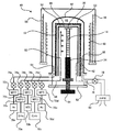
始めに、図1乃至図3を参照して、本発明の第1実施形態に係るSiC成膜装置の構成について一部その動作を交えて説明する。ここに、図1は、本発明の第1実施形態に係るSiC成膜装置の構成を示す斜視図である。
<First Embodiment>
First, with reference to FIG. 1 to FIG. 3, the configuration of the SiC film forming apparatus according to the first embodiment of the present invention will be described with some operations. FIG. 1 is a perspective view showing the configuration of the SiC film forming apparatus according to the first embodiment of the present invention.
本発明の第1実施形態に係るSiC成膜装置としての半導体製造装置10は、バッチ式縦型のSiC成膜装置であり、主要部が配置される筐体12を有する。半導体製造装置10には、例えば、Si又はSiC等で構成された基板としてのウェハ14(図2参照)を収納する基板収納器としてフープ(以下、ポッドという)16が、ウェハキャリアとして使用される。この筐体12の正面側には、ポッドステージ18が配置されており、このポッドステージ18にポッド16が搬送される。ポッド16には、例えば25枚のウェハ14が収納され、蓋が閉じられた状態でポッドステージ18にセットされる。
A
筐体12内の正面側であって、ポッドステージ18に対向する位置にはポッド搬送装置20が配置されている。また、このポッド搬送装置20の近傍にはポッド棚22、ポッドオープナ24及び基板枚数検知器26が配置されている。ポッド棚22はポッドオープナ24の上方に配置されポッド16を複数個載置した状態で保持するように構成されている。基板枚数検知器26はポッドオープナ24に隣接して配置される。ポッド搬送装置20はポッドステージ18とポッド棚22とポッドオープナ24との間でポッド16を搬送する。ポッドオープナ24はポッド16の蓋を開けるものであり、基板枚数検知器26は蓋を開けられたポッド16内のウェハ14の枚数を検知する。
A
筐体12内には基板移載機28、基板支持具としてのボート30が配置されている。基板移載機28は、アーム(ツィーザ)32を有し、図示しない駆動手段により、上下回転動作が可能な構造になっている。アーム32は例えば5枚のウェハを取り出すことができ、このアーム32を動かすことにより、ポッドオープナ24の位置に置かれたポッド16及びボート30間にてウェハ14を搬送する。
A
ボート30は、例えばカーボングラファイトやSiC等の耐熱性材料で構成されており、複数枚のウェハ14を水平姿勢でかつ互いに中心を揃えた状態で整列させて縦方向に積み上げて保持するように構成されている。なお、ボート30の下部には例えばカーボングラファイトや石英やSiC等の耐熱性材料で構成された円盤形状の断熱部材としてのボート断熱部34が配置されており、後述する被加熱体46からの熱が処理炉40の下方側に伝わりにくくなるように構成されている(図2参照)。
The
筐体12内の背面側上部には処理炉40が配置されている。この処理炉40内に複数枚のウェハ14を装填したボート30が搬入され熱処理が行われる。
A
次に、図2を参照しながら、本発明の第1実施形態に係る処理炉40の構成を説明する。図2は、本発明の第1実施形態に係る半導体製造装置10の処理炉40の側面断面図である。
Next, the configuration of the
処理炉40は、円筒形状の反応室44を形成する反応管42を備える。反応管42は、石英またはSiC等の耐熱材料からなり、上端が閉塞し下端が開口した円筒形状に形成されている。反応管42の内側の筒中空部には、反応室44が形成されており、Si又はSiC等で構成された基板としてウェハ14を後述するウェハホルダを介してボート30によって水平姿勢でかつ互いに中心を揃えた状態で整列させて縦方向に積み上げて保持した状態で収納可能に構成されている。
The
反応管42の下方には、この反応管42と同心円状にマニホールドが配設されている。マニホールドはたとえばステンレス等からなり、上端及び下端が開口した円筒形状に形成されている。このマニホールドは反応管42を支持するように設けられている。なお、このマニホールドと反応管42との間にはシール部材としてOリングが設けられている。このマニホールドが図示しない保持体に支持されることにより、反応管42は垂直に据えつけられた状態になっている。この反応管42とマニホールドにより反応容器が形成されている。
Below the
処理炉40は、加熱される被加熱体46及び磁場発生部として誘導加熱源である、たとえば誘導コイル48を備える。被加熱体46は処理室44内に配設されており、該被加熱体は少なくとも基板であるウェハ14の配列領域を囲むように設けられている。この被加熱体46は反応管42の外側に設けられた誘導コイル48により発生される磁場によって加熱される構成となっている。被加熱体46が発熱することにより、処理室44内が加熱される。
The
被加熱体46は、一端(即ち図示上側)が閉塞された筒形状となるように形成されている。これより供給されるガスを封止することができる。更に反応室44上部からの放熱を抑制することができる。
The
被加熱体46の近傍には、反応室44内の温度を検出する温度検出体として図示しない温度センサが設けられている。誘導加熱源としての誘導コイル48及び温度センサには、電気的に図示しない温度制御部が接続されており、温度センサにより検出された温度情報に基づき誘導コイル48への通電具合を調節することにより反応室44内の温度が所定の温度分布となるよう所定のタイミングにて制御するように構成されている。
In the vicinity of the body to be heated 46, a temperature sensor (not shown) is provided as a temperature detector for detecting the temperature in the
被加熱体46と反応管42の間には、例えば誘導されにくいカーボンフェルト等で構成された断熱材50が設けられ、この断熱材50を設けることにより、被加熱体46の熱が反応管42あるいは反応管42の外側へ伝達するのを抑制することができる。
Between the
図2に示されるように、断熱材50は筒形状の側壁部52と、断熱材50の一端(即ち図示上側)を閉塞する蓋部54とで構成されている。これにより、側壁部52と蓋部54とで断熱材50の内側に中空部を設けることができ、その内側に被加熱体46を設ける反応炉構成をつくることができる。また、誘導コイル48が被加熱体46を誘導加熱させて、被加熱体46の内部に載置される基板としてのウェハ14に所定の処理を行う際に発生する被加熱体46からのふく射熱の影響を断熱材50により遮断することができる。また、側壁部52と蓋部54とは別の部材で構成されてもよい。
As shown in FIG. 2, the
また、誘導コイル48の外側には、反応室44内の熱が外側に伝達するのを抑制するための、例えば水冷構造である外側断熱壁56が反応室44を囲むように設けられている。更に、外側断熱壁56の外側には、誘導コイル48により発生された磁場が外側に漏れるのを防止する磁気シール58が設けられている。
Further, outside the
図2に示すように被加熱体46とウェハ14との間に設置され、少なくともSi(シリコン)原子含有ガスとCl(塩素)原子含有ガスとC(炭素)原子含有ガスと還元ガスを供給する第1のガス供給口60と第1の排気口62、反応管42と断熱材50の間に1つの第2のガス供給口64、第2の排気口66が配置されている。それぞれについて詳細に説明をする。
As shown in FIG. 2, it is installed between the object to be heated 46 and the
少なくともSi(シリコン)原子含有ガスとして例えばモノシラン(以下SiH4とする)ガス、Cl(塩素)原子含有ガスとして例えば塩化水素(以下HClとする)ガスとC(炭素)原子含有ガスとして例えばプロパン(以下C3H8とする)ガス、還元ガスとして例えば水素(以下H2とする)ガスとを供給する第1のガス供給口60は、例えばカーボングラファイトで構成され、被加熱体46内側においてウェハ14の側面に設けられており、マニホールドを貫通するようにマニホールドに取り付けられている。
At least Si (silicon) atom-containing gas, for example, monosilane (hereinafter referred to as SiH4) gas, Cl (chlorine) atom-containing gas, for example, hydrogen chloride (hereinafter referred to as HCl) gas, and C (carbon) atom-containing gas, for example, propane (hereinafter, referred to as gas) A first
ガス供給口60は、第1のガスライン68に接続されている。この第1のガスライン68は、例えばSiH4ガス、HClガス、C3H8ガス、H2ガスそれぞれに対して流量制御器(流量制御手段)としてのマスフローコントローラ(以下、MFCとする)72a、72b、72c、72d及びバルブ74a、74b、74c、74dを介して例えばSiH4ガス源70a、HClガス源70b、C3H8ガス源70c、H2ガス源70dに接続されている。
The
この構成により、例えばSiH4ガス、HClガス、C3H8ガス、H2ガスそれぞれの供給流量、濃度、分圧を反応室44内において制御することができる。バルブ74a、74b、74c、74d、MFC72a、72b、72c、72dは、図示しないガス流量制御部によって電気的に接続されており、それぞれ供給するガスの流量が所定流量となるよう、所定のタイミングにて制御するようにされ、例えばSiH4ガス、HClガス、C3H8ガス、H2ガスそれぞれのガス源70a、70b、70c、70d、バルブ74a、74b、74c、74d、MFC72a、72b、72c、72d、第1のガスライン68、第1のガス供給口60によりガス供給系として、第1のガス供給系を構成される。
With this configuration, for example, the supply flow rate, concentration, and partial pressure of each of SiH 4 gas, HCl gas, C 3 H 8 gas, and H 2 gas can be controlled in the
なお、上述はガス供給口60より少なくともSi(シリコン)原子含有ガスとCl(塩素)原子含有ガスとC(炭素)原子含有ガスと還元ガスとを供給したが、これに限らず、それぞれに対応したガス供給口を設けても良く、また、これらのガスは組み合わせて供給できるようにガス供給口を設けても良い。
In the above description, at least the Si (silicon) atom-containing gas, the Cl (chlorine) atom-containing gas, the C (carbon) atom-containing gas, and the reducing gas are supplied from the
なお、Cl(塩素)原子含有ガスとしてHClガスを例示したがCl2ガス(塩素ガス)を用いても良い。 In addition, although HCl gas was illustrated as Cl (chlorine) atom containing gas, you may use Cl2 gas (chlorine gas).
なお、上述では、Si(シリコン)原子含有ガスとCl(塩素)原子含有ガスを供給したが、Si(シリコン)原子とCl(塩素)原子を含むガス、例えば、テトラクロロシラン(以下、SiCl4とする)ガス、トリクロロシラン(以下、SiHCl3とする)ガス、ジクロロシラン(以下SiH2Cl2)ガスを供給しても良い。 In the above description, the Si (silicon) atom-containing gas and the Cl (chlorine) atom-containing gas are supplied. However, a gas containing Si (silicon) atoms and Cl (chlorine) atoms, for example, tetrachlorosilane (hereinafter referred to as SiCl4). ) Gas, trichlorosilane (hereinafter referred to as SiHCl3) gas, or dichlorosilane (hereinafter referred to as SiH2Cl2) gas may be supplied.
なお、C(炭素)原子含有ガスとしてC3H8ガスを例示したが、エチレン(以下C2H4とする)ガス、アセチレン(以下、C2H2とする)ガスを用いても良い。 In addition, although C3H8 gas was illustrated as C (carbon) atom containing gas, you may use ethylene (henceforth C2H4) gas and acetylene (henceforth C2H2) gas.
なお、ガス供給口60から、更にドーパントガスも供給しても良いし、ドーパントガスを供給するためのガス供給口を設けて、ドーパントガスを供給しても良い。
The dopant gas may be further supplied from the
また、第1の排気口62は、第1の供給口60の位置に対して対向面に位置するように配置され、マニホールドには、第1の排気口62に接続されたガス排気管76が貫通するように設けられている。
Further, the
このように、第1のガス供給口60から少なくともSi(シリコン)原子含有ガスとCl(塩素)原子含有ガスとC(炭素)原子含有ガスと還元ガスとを供給し、供給されたガスはSi又はSiCで構成されたウェハ14に対し平行に流れ、第1の排気口62に向かって流れるため、ウェハ14全体が効率的にかつ均一にガスに晒される。
Thus, at least the Si (silicon) atom-containing gas, the Cl (chlorine) atom-containing gas, the C (carbon) atom-containing gas, and the reducing gas are supplied from the first
なお、好ましくは、反応室内であって、被加熱体46とウェハ14との間には第1のガス供給口60と第1の排気口62との間には、図示しない構造物を設けると良い。構造物として、好ましくは断熱材、又はカーボングラファイト材等で構成され、耐熱やパーティクル発生を抑制することができる。これにより、第1のガス供給口60より供給されるガスはウェハ14全体に効率的にかつ均一に晒され、ウェハ14上に成膜されるSiCエピタキシャル膜の膜厚均一性は向上する。
Preferably, a structure (not shown) is provided between the first
第2のガス供給口64は反応管42と断熱材50との間に配置されており、マニホールドを貫通するように取り付けられている。更に第2の排気口66が、反応管42と断熱材50との間に配置され、第2のガス供給口64に対して対向面に位置するように配置され、マニホールドには第2の排気口66に接続されたガス排気管76が貫通するように設けられている。この第2のガス供給口64は不活性ガスとして例えばアルゴン(以下、Arとする)ガスが供給され、SiCエピタキシャル膜成長に寄与するガスとして、例えばSi(シリコン)原子含有ガス又はC(炭素)原子含有ガス又はCl(塩素)原子含有ガス又はそれらの混合ガスが反応管42と断熱材50との間に侵入するのを防ぎ、反応管42の内壁又は断熱材50の外壁に不要な生成物が付着するのを防止することができる。
The second
また、ガス排気管76の下流側には図示しない圧力検出器として圧力センサ及び圧力調整器としてのAPC(Auto Pressure Controller、以下APCとする)バルブ78を介して真空ポンプ等の真空排気装置80が接続されている。圧力センサ及びAPCバルブ78には、図示しない圧力制御部が電気的に接続されており、この圧力制御部は圧力センサにより検出された圧力に基づいて、APCバルブ78の開度を調整することにより、被加熱体46内側の圧力及び反応管42と断熱材50との間の空間の圧力が所定の圧力になるよう、所定のタイミングにて制御するように構成されている。
Further, on the downstream side of the
なお、不活性ガスとしてArガスを例示したが、これに限らず、ヘリウム(以下Heとする)ガス、ネオン(以下Neとする)ガス、クリプトン(以下Krとする)、キセノン(以下Xeとする)等の希ガスより少なくとも1つのガス、又は上述の希ガスより少なくとも1つのガスとの組み合わせされたガスを供給しても良い。 In addition, although Ar gas was illustrated as an inert gas, it is not restricted to this, Helium (hereinafter referred to as He) gas, Neon (hereinafter referred to as Ne) gas, krypton (hereinafter referred to as Kr), xenon (hereinafter referred to as Xe) ) Or the like, or a gas combined with at least one gas from the rare gases described above may be supplied.
次に、処理炉40周辺の構成について説明する。処理炉40の下方には、この処理炉40の下端開口を機密に閉塞するための炉口蓋体としてシールキャップ82が設けられている。シールキャップ82は例えばステンレス等の金属よりなり、円盤状に形成されている。シールキャップ82の上面には処理炉40の下端と当接するシール材としてのOリングが設けられている。シールキャップ82には回転機構84が設けられている。回転機構84の回転軸はシールキャップ82を貫通してボート30に接続されており、このボート30を回転させることで、ウェハ14を回転させるように構成されている。シールキャップ82は処理炉40の外側に向けられた昇降機構として図示しない昇降モータによって垂直方向に昇降されるように構成されており、これにより、ボート30を処理炉40に対し搬入搬出することが可能となっている。回転機構84及び昇降モータには、図示しない駆動制御部が電気的に接続されており、所定の動作をするよう所定のタイミングにて制御するよう構成されている。
Next, the configuration around the
次に、上述したように構成された半導体製造装置10を用いて、半導体デバイスの製造工程の一工程として、例えばSiC等で構成されたウェハなどの基板上に、SiCエピタキシャル膜を形成する方法について説明する。なお、以下の説明において、半導体製造装置10を構成する各部の動作は、図示しないコントローラにより制御される。
Next, as a step of the semiconductor device manufacturing process using the
まず、ポッドステージ18に複数枚のウェハ14を収容したポッド16がセットされると、ポッド搬送装置20によりポッド16をポッドステージ18からポッド棚20へ搬送し、このポッド棚22にストックする。次に、ポッド搬送装置20により、ポッド棚22にストックされたポッド16をポッドオープナ24に搬送してセットし、このポッドオープナ24によりポッド16の蓋を開き、基板枚数検知器26によりポッド16に収容されているウェハ14の枚数を検知する。
First, when a
次に、基板移載機28により、ポッドオープナ24の位置にあるポッド16からウェハ14を取り出し、ボート30に移載する。
Next, the
複数枚のウェハ14がボート30に装填されると、複数枚のウェハ14を保持したボート30は、昇降モータによる図示しない昇降台及び昇降シャフトの昇降動作により反応室44内に搬入(ボートローディング)される。この状態で、シールキャップ82はOリングを介してマニホールドの下端をシールした状態となる。
When a plurality of
被加熱体46内側が所定の圧力(真空度)となるように真空排気装置80によって真空排気される。この際、被加熱体46内側の圧力は、圧力センサで測定され、この測定された圧力に基づき第1の排気口62及第2の排気口66に連通するAPCバルブ78がフィードバック制御される。また、ウェハ14及び被加熱体46内側が所定の温度となるように誘導加熱源としての誘導コイル48により加熱され、被加熱体46、基板であるウェハ14が加熱される。この際、被加熱体46内側が所定の温度分布となるように温度センサが検出した温度情報に基づき誘導コイル48への通電具合がフィードバック制御される。続いて、回転機構84により、ボート30が回転されることでウェハ14が周方向に回転される。
The inside of the object to be heated 46 is evacuated by the
続いて、SiCエピタキシャル成長反応に寄与するSi(シリコン)原子含有ガス及びCl(塩素)原子含有ガス、C(炭素)原子含有ガス及び還元ガスであるH2ガスはそれぞれ、ガス源70a、70b、70c、70dから供給され、被加熱体46内側に少なくとも1つ設けられる第1のガス供給口60より被加熱体46内側に噴出され、SiCエピタキシャル成長反応が行われる。
Subsequently, the Si (silicon) atom-containing gas, the Cl (chlorine) atom-containing gas, the C (carbon) atom-containing gas, and the H2 gas that is a reducing gas that contribute to the SiC epitaxial growth reaction are respectively supplied to the
このとき、Si(シリコン)原子含有ガス及びCl(塩素)原子含有ガス及び、C(炭素)原子含有ガス及び還元ガスであるH2ガスは、所定の流量となるように対応するMFC72a、72b、72c、72dの開度が調整された後、バルブ74a、74b、74c、74dが開かれ、それぞれのガスが第1のガスライン68を流通して、第1のガス供給口60から被加熱体46内側に供給される。
At this time, the Si (silicon) atom-containing gas, the Cl (chlorine) atom-containing gas, the C (carbon) atom-containing gas, and the H2 gas that is the reducing gas correspond to MFCs 72a, 72b, 72c corresponding to predetermined flow rates. 72d, the
第1のガス供給口60より供給されたガスは、反応室44内の被加熱体46内側を通り、第1の排気口62からガス排気管76を通り排気される。供給されたガスは、被加熱体46内側を通過する際にウェハ14の側面から供給され、ウェハ14と接触しウェハ14の表面上にSiCエピタキシャル膜成長がなされる。
The gas supplied from the first
またガス供給源70eより不活性ガスである例えばArガスは所定の流量となるように、対応するMFC72eの開度が調整された後、バルブ74eが開かれ、ガス供給管を流通して、第2のガス供給口64から反応管42と断熱材50との間に形成される空間に供給される。第2のガス供給口64から供給された不活性ガスであるArガスは、処理室44内の断熱材50と反応管42との間に形成される空間を通過し、第2の排気口66から排気される。
Further, after the opening degree of the corresponding
SiCエピタキシャル膜成長は、予め設定された時間が経過すると、上述のガスの供給を停止し、図示しない不活性ガス供給源から不活性ガスが供給され、被加熱体46内側が不活性ガスで置換されると共に、処理室44内の圧力が常圧に復帰される。
In the SiC epitaxial film growth, when a preset time elapses, the supply of the gas is stopped, an inert gas is supplied from an inert gas supply source (not shown), and the inside of the object to be heated 46 is replaced with the inert gas. At the same time, the pressure in the
その後、昇降モータによりシールキャップ82が下降されて、マニホールドの下端が開口されると共に、処理済ウェハ14がボート30に保持された状態でマニホールドの下端から反応管42の外部に搬出(ボートアンローディング)し、ボート30に支持された全てのウェハ14が冷えるまで、ボート30を所定位置で待機させる。次に、待機させたボート30のウェハ14が所定温度まで冷却されると、基板移載機28により、ボート30からウェハ14を取り出し、ポッドオープナ24にセットされている空のポッド16に搬送して収容する。その後、ポッド搬送装置20により、ウェハ14が収容されたポッド16をポッド棚22、またはポッドステージ18に搬送する。このようにして半導体製造装置10の一連の作用が完了する。
Thereafter, the
次に、図3を参照しながら、本発明の第1実施形態に係るウェハ14及びウェハホルダの詳細について説明する。図3は、本発明の第1実施形態に係るウェハ14及びウェハホルダの拡大詳細図である。
Next, details of the
本発明の第1実施形態に係るウェハホルダは、略円板状のウェハホルダ上100であり、ボート30の柱に支持されたウェハ14の裏面(即ち図示上面)を覆うように構成されている。ウェハホルダ上100は、ウェハ14の裏面を覆うように形成された内周部104と、内周部104より厚い外周部102を有している、即ちウェハホルダ上100は、その側面断面形状が逆凹型となるように構成されている。
The wafer holder according to the first embodiment of the present invention is a substantially disk-shaped
図3に示されるように、外周部102と内周部104との厚さの差は、ウェハ14の厚さより小さくなるように構成されている。即ち、ウェハホルダ上100は、ウェハ14により支持され、その内周部104がウェハ14の裏面に接するように構成されている。従って、ウェハ14の裏面にはガスが流入する隙間がなくウェハ14の裏面に接する内周部104全体が「ガス流入抑制部」を構成する。このように、本発明に係る「ガス流入抑制部」の一例たる内周部104が設けられることで、ウェハ14の裏面への反応ガスの回り込みが抑制され、ウェハ14の裏面へのSiC膜の形成を抑制できる。
As shown in FIG. 3, the difference in thickness between the outer
本発明の第1実施形態において、ウェハホルダ上100の態様は、ウェハ14の裏面への反応ガスの流入を抑止するようにウェハ14の周囲を囲うように設けられたガス流入抑止部を有することが可能である限りにおいて、特に限定されず各種の態様を有してよい。
In the first embodiment of the present invention, the aspect of the
<第2実施形態>
次に、図4乃至図6を参照しながら第2実施形態に係るウェハホルダについて説明する。ここに、図4は、本発明の第2実施形態に係るウェハ14及びウェハホルダの構成を示す分解斜視図であり、図5は、本発明の第2実施形態に係るウェハ14及びウェハホルダの拡大詳細図であり、図6は、本発明の第2実施形態に係るウェハホルダ下の拡大詳細図である。なお、図4乃至図6において、図3と重複する箇所には同一の符合を付してその説明を適宜省略することとする。
Second Embodiment
Next, a wafer holder according to the second embodiment will be described with reference to FIGS. FIG. 4 is an exploded perspective view showing the configuration of the
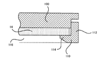
第1実施形態では、ウェハホルダがウェハホルダ上100のみを有するように構成されていたが、第2実施形態では、図4及び図5に示されるように、ウェハ14の裏面を覆うように形成された略円板状のウェハホルダ上100と、ウェハ14を支持するとともにウェハ14の正面(即ち図示下面)へ反応ガスを回り込ませるように形成された略環状のウェハホルダ下110とを有するように構成されている。
In the first embodiment, the wafer holder is configured to have only the wafer holder upper 100, but in the second embodiment, as shown in FIGS. 4 and 5, the wafer holder is formed so as to cover the back surface of the
図5に示されるように、第2実施形態に係るウェハホルダ上100は、その外周部102が内周部104より薄くなる、即ち側面断面形状が逆凸型となるように構成されている。ウェハホルダ下110は、その外周部112が内周部114より厚くなる、即ち側面断面形状が略凹型となるように構成されている。
As shown in FIG. 5, the
本発明の第2実施形態に係るウェハホルダは、ウェハホルダ下110を有しているため、基板移載機28のアーム(ツィーザ)32は、ウェハホルダ下110を保持することになり、ウェハ14を触らずにボート30に移載することが可能となる。
Since the wafer holder according to the second embodiment of the present invention has the
また、ウェハホルダ下110の外周部112と内周部114との厚さの差と、ウェハホルダ上100の外周部102と内周部104との厚さの差との差は、ウェハ14の厚さより小さくなるように構成するとよい。即ち、ウェハホルダ上100とウェハホルダ下110とが組み合わされた場合、ウェハホルダ上100は、ウェハ14により支持され、その内周部104(即ち図示下側に向けた突出部)がウェハ14の裏面に接するように構成されている。従って、ウェハ14の裏面にはガスが流入する隙間がなくウェハ14の裏面に接する内周部104全体が「ガス流入抑制部」を構成する。このように、本発明に係る「ガス流入抑制部」の一例たる内周部104が設けられることで、ウェハ14の裏面への反応ガスの回り込みが抑制され、ウェハ14の裏面へのSiC膜の形成を抑制できる。
Further, the difference between the thickness difference between the outer
また、ウェハホルダ上100とウェハホルダ下110とが組み合わされた場合は、ウェハホルダ上100の内周部104の先端(即ち図示下側に向けた突出部の下面)は、ウェハホルダ下110の外周部112の上端(即ち図示上側に向けた上面)より下に位置するように構成されるとよい。この構成によれば、反応ガスが横から吹き付けられたとしても、ウェハホルダ上100がウェハホルダ下110から外れることを防止することができる。特にSiC基板は滑りやすく、有効な構成となる。また、本発明の第2実施形態のウェハホルダ上100とウェハホルダ下110の構成によれば、第1実施形態に係るウェハホルダと比較して、ウェハホルダ全体の厚さは大きくなるものの、嵌合する量を自由に設計でき、ウェハホルダ上が横から吹き付けられる反応ガスにより外れてしまうことを防止できる。
When the
本発明の第2実施形態においては、ウェハホルダ上100の態様は、ウェハ14の裏面への反応ガスの流入を抑止するようにウェハ14の周囲を囲うように設けられたガス流入抑止部を有することが可能である限りにおいて、特に限定されず各種の態様を有してよい。
In the second embodiment of the present invention, the aspect of the wafer holder upper 100 has a gas inflow suppressing portion provided so as to surround the periphery of the
また、図6に示されるように、ウェハホルダ下110の下面は、ウェハホルダ下110の中心部116に向かって薄くなるように構成されるとよい。この構成によれば、横から吹き付けられるガスの流れをウェハ14の成膜面(即ち図示下面)に向かわせるためにガイドすることができる。
Further, as shown in FIG. 6, the lower surface of the
なお、ウェハホルダ下110の下面の態様は、横から吹き付けられるガスの流れをウェハ14の成膜面(即ち図示下面)に向かわせるためにガイドすることが可能である限りにおいて、特に限定されず各種の態様を有してよい。例えば、ウェハホルダ下110の下面は、図6に示されるように、ウェハホルダ下110の内周部114の下面のみがウェハホルダ下110の中心部116に向かって薄くなるように形成されているが、ウェハホルダ下110の外周面112及び内周面114が共にウェハホルダ下110の中心部116に向かって薄くなるように形成されてもよい。
The aspect of the lower surface of the
<第3実施形態>
次に、図7を参照しながら、本発明の第3実施形態について説明する。図7は、本発明の第3実施形態に係るウェハ14及びウェハホルダの拡大詳細図である。同図において、図6と重複する箇所には同一の符合を付してその説明を適宜省略することとする。
<Third Embodiment>
Next, a third embodiment of the present invention will be described with reference to FIG. FIG. 7 is an enlarged detailed view of the
上述した本発明の第2実施形態の変形例として、本発明の第3実施形態では、ウェハホルダ上100の内周部104の外側には、ウェハホルダ上100の外周部102より厚く、かつ、内周部104の中心部より厚いリング状の突出部106が形成されている。従って、ウェハホルダ上100とウェハホルダ下110が組み合わされた場合は、リング状の突出部106がウェハ14の裏面と接触することによって、ウェハ14の裏面への反応ガスの回り込みが抑制され、ウェハ14の裏面へのSiC膜の形成を抑制できる。従って、ウェハ14の裏面に接するリング状の突出部106が「ガス流入阻止部」を構成する。
As a modification of the second embodiment of the present invention described above, in the third embodiment of the present invention, the outer periphery of the inner
このように、ウェハホルダ上100の内周部104にリング状の突出部106を形成することで、ウェハホルダ上100の内周部104の中心部とウェハ14の裏面との間に、中空部120が形成されている。これによって、ウェハホルダ上100とウェハ14の裏面との接触面積を低減している。よって、ウェハ14とウェハホルダ上100との貼り付きを抑制することができる。
Thus, by forming the ring-shaped protruding
なお、本発明の第3実施形態において、ウェハホルダ上100の内周部104とウェハ14の裏面との間に中空部120が形成されていたが、ウェハホルダ上100の態様は、ウェハ14の裏面への反応ガスの流入を抑止するようにウェハ14の周囲を囲うように設けられたガス流入抑止部を有することが可能である限りにおいて、特に限定されず各種の態様を有してよい。例えば、ウェハホルダ上100の内周部104には、上述したウェハ14の裏面に接触する突出部106が設けられなく、ウェハホルダ上100の外周部102とウェハホルダ下110の外周部112とを接触させ、ウェハホルダ上100の内周部104をウェハ14の裏面に全く接触させないように形成されてもよい。
In the third embodiment of the present invention, the
また、本発明の第3実施形態では、中空部120が処理炉40の内部を真空に引いた際の空気溜りとなり、真空度到達時間に影響を与える可能性がある。そこで、完全な中空部にせずに空気の流通口を形成してもよい。この際、この形成された流通口を介してウェハ14の裏面へ到達する反応ガスの量が少なくなり、成膜される膜の厚さも薄くなるため、研磨工程の時間も少なくなり、結果としてスループットも向上できる。即ち、中空部120及び流通口を形成することによって、成膜工程のスループットを向上する共に、真空成膜の真空度を維持することができる。
Moreover, in 3rd Embodiment of this invention, the
〔付記〕
以下に、本実施形態に係る好ましい態様を付記する。
[Appendix]
Below, the preferable aspect which concerns on this embodiment is appended.
〔付記1〕
複数のウェハを保持するボートと、前記ボートに保持された前記複数のウェハの側面から反応ガスを供給する反応ガス供給部とを有する成膜装置に用いられるウェハホルダであって、前記ウェハホルダは、前記ボートに保持された際に前記ウェハの上面を覆うように載置され、前記ウェハの裏面への前記反応ガスの流入を抑止するように前記ウェハの周囲を囲うように設けられたガス流入抑止部を有するウェハホルダ上を具備するウェハホルダ。
[Appendix 1]
A wafer holder for use in a film forming apparatus having a boat for holding a plurality of wafers, and a reaction gas supply unit for supplying a reaction gas from a side surface of the plurality of wafers held in the boat, A gas inflow restraint unit that is placed so as to cover the upper surface of the wafer when held on the boat and surrounds the periphery of the wafer so as to restrain the reaction gas from flowing into the back surface of the wafer. A wafer holder comprising:
〔付記2〕
付記1において、前記ガス流入抑止部は、前記ウェハにより支持されるウェハホルダ。
[Appendix 2]
In Appendix 1, the gas inflow suppression part is a wafer holder supported by the wafer.
〔付記3〕
付記2において、前記ウェハホルダ上は、ウェハホルダ上の外周部がウェハホルダ上の内周部より厚い凹型をしており、前記ウェハホルダ上の内周部の上面から前記ウェハホルだの外周部の先端面までの高さは、前記ウェハの厚さより小さく、前記ウェハホルダ上の内周部が前記ウェハに接触することによりガス流入抑止部を形成するウェハホルダ。
[Appendix 3]
In Supplementary Note 2, the wafer holder has a concave shape in which the outer peripheral portion on the wafer holder is thicker than the inner peripheral portion on the wafer holder, and from the upper surface of the inner peripheral portion on the wafer holder to the front end surface of the outer peripheral portion of the wafer holder A wafer holder having a height smaller than the thickness of the wafer and forming a gas inflow restraint portion when an inner peripheral portion on the wafer holder contacts the wafer.
〔付記4〕
付記2において、前記ウェハホルダは、前記ウェハを保持するウェハホルダ下を更に有し、前記ウェハホルダ下が前記ボートに支持されるウェハホルダ。
[Appendix 4]
The wafer holder according to appendix 2, wherein the wafer holder further has a lower wafer holder for holding the wafer, and the lower wafer holder is supported by the boat.
〔付記5〕
付記4において、前記ウェハホルダ上は、ウェハホルダ上の外周部がウェハホルダ上の内周部より薄い凸型をしており、前記ウェハホルダ下は、ウェハホルダ下の外周部がウェハホルダ下の内周部より厚い円環状の凹型をしており、前記ウェハホルダ上と前記ウェハホルダ下が組み合わされた際に、前記ウェハホルダの上の内周部の先端面が前記ウェハホルダ下の外周部の先端面より下に位置するウェハホルダ。
[Appendix 5]
In Supplementary Note 4, the wafer holder has a convex shape in which the outer peripheral part on the wafer holder is thinner than the inner peripheral part on the wafer holder, and the outer peripheral part below the wafer holder is thicker than the inner peripheral part below the wafer holder on the wafer holder. A wafer holder, which has an annular concave shape, and has a tip surface of an inner peripheral portion on the wafer holder located below a tip surface of an outer peripheral portion under the wafer holder when the wafer holder and the wafer holder are combined.
〔付記6〕
付記5において、前記ウェハホルダ上と前記ウェハホルダ下が組み合わされた際に、前記ウェハホルダ上の内周部の先端面が、前記ウェハホルダ下に保持されたウェハの裏面に接触することにより前記ガス流入抑止部を形成するウェハホルダ。
[Appendix 6]
In Supplementary Note 5, when the top of the wafer holder and the bottom of the wafer holder are combined, the front end surface of the inner peripheral portion on the wafer holder comes into contact with the back surface of the wafer held under the wafer holder, whereby the gas inflow suppression portion Forming a wafer holder.
〔付記7〕
付記4において、前記ウェハホルダ下の下面は、前記ウェハホルダ下の中心部に向かって薄くなるウェハホルダ。
[Appendix 7]
The wafer holder according to appendix 4, wherein the lower surface under the wafer holder becomes thinner toward the center under the wafer holder.
〔付記8〕
付記4において、前記ウェハホルダ上は、ウェハホルダ上の外周部より厚く、かつ、ウェハホルダ上の中心部より厚いリング状の突出部を有し、前記ウェハホルダ上と前記ウェハホルダ下が組み合わされた際に、前記リング状の突出部がウェハの裏面と接触することにより前記ガス流入抑止部を形成するウェハホルダ。
[Appendix 8]
In Supplementary Note 4, the wafer holder has a ring-shaped protrusion that is thicker than the outer peripheral portion on the wafer holder and thicker than the center portion on the wafer holder, and when the wafer holder and the lower portion of the wafer holder are combined, A wafer holder that forms the gas inflow restraint portion by a ring-shaped protrusion contacting a back surface of a wafer.
〔付記9〕
付記1において、前記ウェハホルダは、前記ボートに支持されると共に前記ウェハを保持するウェハホルダ下を更に有し、前記ウェハホルダ上の外周部と前記ウェハホルダ下の外周部とが接触することにより前記ガス流入抑止部を形成するウェハホルダ。
[Appendix 9]
In Supplementary Note 1, the wafer holder further includes a wafer holder below the wafer holder that is supported by the boat and holds the wafer, and the outer periphery of the wafer holder is in contact with the outer periphery of the wafer holder so that the gas inflow is suppressed. Wafer holder forming part.
〔付記10〕
処理されるべきウェハを保持した、付記1〜9のいずれか一つに記載のウェハホルダを複数保持するボートと、前記ボートに保持された前記複数のウェハの側面から反応ガスを供給する反応ガス供給部とを有する成膜装置。
[Appendix 10]
A boat that holds a plurality of wafer holders according to any one of appendices 1 to 9 that holds a wafer to be processed, and a reactive gas supply that supplies a reactive gas from a side surface of the plurality of wafers held in the boat A film forming apparatus.
〔付記11〕
ウェハの裏面への反応ガスの流入を抑止するようにウェハの周囲を囲うように設けられたガス流入抑止部を有するウェハホルダ上をウェハの上面を覆うように載置するウェハホルダ載置工程と、前記ウェハホルダ上が載置された状態でボート移載に移載工程と、前記ボートを反応室内に移動するボートローディング工程と、反応ガスを供給し、前記ウェハの下面に膜を形成する成膜工程とを有する成膜方法。
[Appendix 11]
A wafer holder placing step of placing a wafer holder on a wafer holder having a gas inflow restraining portion provided so as to surround the periphery of the wafer so as to inhibit the inflow of reaction gas to the back surface of the wafer; A transfer process for transferring a boat with the wafer holder placed thereon, a boat loading process for moving the boat into a reaction chamber, a film forming process for supplying a reaction gas and forming a film on the lower surface of the wafer; A film forming method comprising:
本発明に係るウェハホルダ及び成膜方法は、SiCエピタキシャル膜を基板上に成膜する成膜装置に用いられるウェハホルダ及び成膜方法に利用可能である。 The wafer holder and film forming method according to the present invention can be used for a wafer holder and film forming method used in a film forming apparatus for forming a SiC epitaxial film on a substrate.
10 半導体製造装置
12 筐体
14 ウェハ
16 ポッド
30 ボート
40 処理炉
42 反応管
44 処理室
46 被加熱体
48 磁気コイル
50 断熱部
56 外側断熱壁
60 第1のガス供給口
62 第1の排気口
100 ウェハホルダ上
102 外周部
104 内周部
106 突出部
110 ウェハホルダ下
112 外周部
114 内周部
116 中心部
120 中空部
DESCRIPTION OF
Claims (2)
前記ウェハホルダは、前記ボートに保持された際に前記ウェハの上面を覆うように載置され、前記ウェハの裏面への前記反応ガスの流入を抑止するように前記ウェハの周囲を囲うように設けられたガス流入抑止部を有するウェハホルダ上を具備する成膜装置。 A boat that holds a plurality of wafer holders in a state where wafers are mounted, and a reaction gas supply unit that supplies a reaction gas from a side surface of the plurality of wafers held in the boat,
The wafer holder is placed so as to cover the upper surface of the wafer when held by the boat, and is provided so as to surround the periphery of the wafer so as to prevent the reaction gas from flowing into the back surface of the wafer. A film forming apparatus comprising a wafer holder having a gas inflow suppressing portion.
前記ウェハホルダ上が載置された状態でボート移載に移載工程と、
前記ボートを反応室内に移動するボートローディング工程と、
反応ガスを供給し、前記ウェハの下面に膜を形成する成膜工程とを有する成膜方法。 A wafer holder placing step of placing the wafer holder on the wafer holder so as to cover the upper surface of the wafer, having a gas inflow restraining portion provided so as to surround the periphery of the wafer so as to inhibit the inflow of the reaction gas to the back surface of the wafer;
A transfer process to the boat transfer in a state where the wafer holder is mounted;
A boat loading step of moving the boat into the reaction chamber;
A film forming method including supplying a reaction gas and forming a film on a lower surface of the wafer.
Priority Applications (2)
| Application Number | Priority Date | Filing Date | Title |
|---|---|---|---|
| JP2010211878A JP2012069635A (en) | 2010-09-22 | 2010-09-22 | Deposition device, wafer holder and deposition method |
| US13/036,304 US20120067274A1 (en) | 2010-09-22 | 2011-02-28 | Film forming apparatus, wafer holder, and film forming method |
Applications Claiming Priority (1)
| Application Number | Priority Date | Filing Date | Title |
|---|---|---|---|
| JP2010211878A JP2012069635A (en) | 2010-09-22 | 2010-09-22 | Deposition device, wafer holder and deposition method |
Publications (2)
| Publication Number | Publication Date |
|---|---|
| JP2012069635A true JP2012069635A (en) | 2012-04-05 |
| JP2012069635A5 JP2012069635A5 (en) | 2013-10-31 |
Family
ID=45816560
Family Applications (1)
| Application Number | Title | Priority Date | Filing Date |
|---|---|---|---|
| JP2010211878A Pending JP2012069635A (en) | 2010-09-22 | 2010-09-22 | Deposition device, wafer holder and deposition method |
Country Status (2)
| Country | Link |
|---|---|
| US (1) | US20120067274A1 (en) |
| JP (1) | JP2012069635A (en) |
Cited By (3)
| Publication number | Priority date | Publication date | Assignee | Title |
|---|---|---|---|---|
| US9716010B2 (en) | 2013-11-12 | 2017-07-25 | Globalfoundries Inc. | Handle wafer |
| JP2019192688A (en) * | 2018-04-19 | 2019-10-31 | 三菱電機株式会社 | Wafer boat and method of manufacturing the same |
| WO2020158657A1 (en) * | 2019-02-01 | 2020-08-06 | 東京エレクトロン株式会社 | Film forming apparatus and film forming method |
Families Citing this family (6)
| Publication number | Priority date | Publication date | Assignee | Title |
|---|---|---|---|---|
| TWI575631B (en) | 2011-06-28 | 2017-03-21 | Dynamic Micro Systems | Semiconductor stocker systems and methods |
| JP5906318B2 (en) * | 2012-08-17 | 2016-04-20 | 株式会社Ihi | Manufacturing method and manufacturing apparatus for heat-resistant composite material |
| WO2014191621A1 (en) * | 2013-05-29 | 2014-12-04 | Beneq Oy | Substrate carrier and arrangement for supporting substrates |
| DE112015004190A5 (en) * | 2014-11-26 | 2017-06-14 | Von Ardenne Gmbh | Substrate holding device, substrate transport device, processing device and method for processing a substrate |
| US10712005B2 (en) * | 2017-07-14 | 2020-07-14 | Goodrich Corporation | Ceramic matrix composite manufacturing |
| US10790466B2 (en) * | 2018-12-11 | 2020-09-29 | Feng-wen Yen | In-line system for mass production of organic optoelectronic device and manufacturing method using the same system |
Citations (3)
| Publication number | Priority date | Publication date | Assignee | Title |
|---|---|---|---|---|
| JP2002222806A (en) * | 2001-01-26 | 2002-08-09 | Ebara Corp | Substrate processor |
| JP2004055672A (en) * | 2002-07-17 | 2004-02-19 | Nikko Materials Co Ltd | Chemical vapor deposition apparatus and method |
| JP2004172374A (en) * | 2002-11-20 | 2004-06-17 | Shin Etsu Handotai Co Ltd | Holding jig, manufacturing method of semiconductor wafer, and method for mounting semiconductor substrate and holding jig |
Family Cites Families (3)
| Publication number | Priority date | Publication date | Assignee | Title |
|---|---|---|---|---|
| US5262029A (en) * | 1988-05-23 | 1993-11-16 | Lam Research | Method and system for clamping semiconductor wafers |
| DE4305750C2 (en) * | 1993-02-25 | 2002-03-21 | Unaxis Deutschland Holding | Device for holding flat, circular disk-shaped substrates in the vacuum chamber of a coating or etching system |
| JPH08153682A (en) * | 1994-11-29 | 1996-06-11 | Nec Corp | Plasma cvd device |
-
2010
- 2010-09-22 JP JP2010211878A patent/JP2012069635A/en active Pending
-
2011
- 2011-02-28 US US13/036,304 patent/US20120067274A1/en not_active Abandoned
Patent Citations (3)
| Publication number | Priority date | Publication date | Assignee | Title |
|---|---|---|---|---|
| JP2002222806A (en) * | 2001-01-26 | 2002-08-09 | Ebara Corp | Substrate processor |
| JP2004055672A (en) * | 2002-07-17 | 2004-02-19 | Nikko Materials Co Ltd | Chemical vapor deposition apparatus and method |
| JP2004172374A (en) * | 2002-11-20 | 2004-06-17 | Shin Etsu Handotai Co Ltd | Holding jig, manufacturing method of semiconductor wafer, and method for mounting semiconductor substrate and holding jig |
Cited By (4)
| Publication number | Priority date | Publication date | Assignee | Title |
|---|---|---|---|---|
| US9716010B2 (en) | 2013-11-12 | 2017-07-25 | Globalfoundries Inc. | Handle wafer |
| JP2019192688A (en) * | 2018-04-19 | 2019-10-31 | 三菱電機株式会社 | Wafer boat and method of manufacturing the same |
| JP7030604B2 (en) | 2018-04-19 | 2022-03-07 | 三菱電機株式会社 | Wafer boat and its manufacturing method |
| WO2020158657A1 (en) * | 2019-02-01 | 2020-08-06 | 東京エレクトロン株式会社 | Film forming apparatus and film forming method |
Also Published As
| Publication number | Publication date |
|---|---|
| US20120067274A1 (en) | 2012-03-22 |
Similar Documents
| Publication | Publication Date | Title |
|---|---|---|
| JP2012069635A (en) | Deposition device, wafer holder and deposition method | |
| US9074284B2 (en) | Heat treatment apparatus | |
| JP5735304B2 (en) | Substrate processing apparatus, substrate manufacturing method, semiconductor device manufacturing method, and gas supply pipe | |
| JP5564311B2 (en) | Semiconductor device manufacturing method, substrate processing apparatus, and substrate manufacturing method | |
| US20110306212A1 (en) | Substrate processing apparatus, semiconductor device manufacturing method and substrate manufacturing method | |
| JP5562409B2 (en) | Semiconductor device manufacturing method, substrate manufacturing method, and substrate processing apparatus | |
| US20120214317A1 (en) | Substrate processing apparatus and method, and semiconductor device manufacturing method | |
| JP2012195565A (en) | Substrate processing apparatus, substrate processing method, and manufacturing method of semiconductor device | |
| US20100282166A1 (en) | Heat treatment apparatus and method of heat treatment | |
| JP2011205059A (en) | Method of manufacturing semiconductor device, method of manufacturing substrate and substrate processing apparatus | |
| JP2012178492A (en) | Substrate processing device, gas nozzle, and method of manufacturing substrate or semiconductor device | |
| JP2013197474A (en) | Substrate processing method, semiconductor device manufacturing method and substrate processing apparatus | |
| JP5632190B2 (en) | Semiconductor device manufacturing method, substrate manufacturing method, and substrate processing apparatus | |
| JP2015018869A (en) | Substrate processing apparatus | |
| WO2012120991A1 (en) | Substrate processing apparatus and method for manufacturing substrate | |
| JP2012193985A (en) | Substrate processing device and manufacturing method for substrate | |
| JP2013207057A (en) | Substrate processing apparatus, substrate manufacturing method, and substrate processing apparatus cleaning method | |
| JP2013197507A (en) | Substrate processing apparatus, substrate processing method, and semiconductor device manufacturing method | |
| JP2012178390A (en) | Substrate processing apparatus | |
| JP2012175077A (en) | Substrate processing device, method of manufacturing substrate, and method of manufacturing semiconductor device | |
| JP2012191191A (en) | Substrate processing apparatus | |
| JP2012195355A (en) | Substrate processing device and substrate manufacturing method | |
| JP2011216848A (en) | Method of manufacturing semiconductor device, and manufacturing method and processing apparatus for substrate | |
| JP2012175072A (en) | Substrate processing apparatus | |
| JP2014179550A (en) | Substrate processing apparatus |
Legal Events
| Date | Code | Title | Description |
|---|---|---|---|
| A521 | Written amendment |
Free format text: JAPANESE INTERMEDIATE CODE: A523 Effective date: 20130912 |
|
| A621 | Written request for application examination |
Free format text: JAPANESE INTERMEDIATE CODE: A621 Effective date: 20130912 |
|
| A977 | Report on retrieval |
Free format text: JAPANESE INTERMEDIATE CODE: A971007 Effective date: 20140425 |
|
| A131 | Notification of reasons for refusal |
Free format text: JAPANESE INTERMEDIATE CODE: A131 Effective date: 20140508 |
|
| A02 | Decision of refusal |
Free format text: JAPANESE INTERMEDIATE CODE: A02 Effective date: 20141002 |