EP2890835B1 - Verfahren zur abscheidung einer aluminiumnitridschicht - Google Patents
Verfahren zur abscheidung einer aluminiumnitridschicht Download PDFInfo
- Publication number
- EP2890835B1 EP2890835B1 EP13777342.0A EP13777342A EP2890835B1 EP 2890835 B1 EP2890835 B1 EP 2890835B1 EP 13777342 A EP13777342 A EP 13777342A EP 2890835 B1 EP2890835 B1 EP 2890835B1
- Authority
- EP
- European Patent Office
- Prior art keywords
- substrate
- aluminium
- depositing
- nitride layer
- vacuum chamber
- Prior art date
- Legal status (The legal status is an assumption and is not a legal conclusion. Google has not performed a legal analysis and makes no representation as to the accuracy of the status listed.)
- Active
Links
Images
Classifications
-
- H10P14/3416—
-
- C—CHEMISTRY; METALLURGY
- C30—CRYSTAL GROWTH
- C30B—SINGLE-CRYSTAL GROWTH; UNIDIRECTIONAL SOLIDIFICATION OF EUTECTIC MATERIAL OR UNIDIRECTIONAL DEMIXING OF EUTECTOID MATERIAL; REFINING BY ZONE-MELTING OF MATERIAL; PRODUCTION OF A HOMOGENEOUS POLYCRYSTALLINE MATERIAL WITH DEFINED STRUCTURE; SINGLE CRYSTALS OR HOMOGENEOUS POLYCRYSTALLINE MATERIAL WITH DEFINED STRUCTURE; AFTER-TREATMENT OF SINGLE CRYSTALS OR A HOMOGENEOUS POLYCRYSTALLINE MATERIAL WITH DEFINED STRUCTURE; APPARATUS THEREFOR
- C30B25/00—Single-crystal growth by chemical reaction of reactive gases, e.g. chemical vapour-deposition growth
- C30B25/02—Epitaxial-layer growth
- C30B25/06—Epitaxial-layer growth by reactive sputtering
-
- C—CHEMISTRY; METALLURGY
- C30—CRYSTAL GROWTH
- C30B—SINGLE-CRYSTAL GROWTH; UNIDIRECTIONAL SOLIDIFICATION OF EUTECTIC MATERIAL OR UNIDIRECTIONAL DEMIXING OF EUTECTOID MATERIAL; REFINING BY ZONE-MELTING OF MATERIAL; PRODUCTION OF A HOMOGENEOUS POLYCRYSTALLINE MATERIAL WITH DEFINED STRUCTURE; SINGLE CRYSTALS OR HOMOGENEOUS POLYCRYSTALLINE MATERIAL WITH DEFINED STRUCTURE; AFTER-TREATMENT OF SINGLE CRYSTALS OR A HOMOGENEOUS POLYCRYSTALLINE MATERIAL WITH DEFINED STRUCTURE; APPARATUS THEREFOR
- C30B25/00—Single-crystal growth by chemical reaction of reactive gases, e.g. chemical vapour-deposition growth
- C30B25/02—Epitaxial-layer growth
- C30B25/18—Epitaxial-layer growth characterised by the substrate
- C30B25/186—Epitaxial-layer growth characterised by the substrate being specially pre-treated by, e.g. chemical or physical means
-
- C—CHEMISTRY; METALLURGY
- C30—CRYSTAL GROWTH
- C30B—SINGLE-CRYSTAL GROWTH; UNIDIRECTIONAL SOLIDIFICATION OF EUTECTIC MATERIAL OR UNIDIRECTIONAL DEMIXING OF EUTECTOID MATERIAL; REFINING BY ZONE-MELTING OF MATERIAL; PRODUCTION OF A HOMOGENEOUS POLYCRYSTALLINE MATERIAL WITH DEFINED STRUCTURE; SINGLE CRYSTALS OR HOMOGENEOUS POLYCRYSTALLINE MATERIAL WITH DEFINED STRUCTURE; AFTER-TREATMENT OF SINGLE CRYSTALS OR A HOMOGENEOUS POLYCRYSTALLINE MATERIAL WITH DEFINED STRUCTURE; APPARATUS THEREFOR
- C30B29/00—Single crystals or homogeneous polycrystalline material with defined structure characterised by the material or by their shape
- C30B29/10—Inorganic compounds or compositions
- C30B29/40—AIIIBV compounds wherein A is B, Al, Ga, In or Tl and B is N, P, As, Sb or Bi
- C30B29/403—AIII-nitrides
-
- H10P14/22—
-
- H10P14/2905—
-
- H10P14/2926—
-
- H10P14/3241—
-
- H10P14/3602—
-
- H10P50/242—
Definitions
- a method for depositing an aluminium nitride layer is described herein.
- AlGaN/GaN based semiconductors are used in various devices such as light emitting diodes, laser diodes, photovoltaic solar cells and power devices such as high electron mobility transistors.
- the basic structure of a light emitting diode corresponds to a pn-semiconductor diode so that they exhibit comparable characteristics. A difference lies in the semiconductor materials used for LEDs. While non-luminescent diodes are manufactured from silicon, or sometimes germanium or selenium, the semiconductor material for LEDs is a III-V semiconductor, usually a gallium compound.
- the wavelength of the light emitted depends on the band gap energy of the materials forming the pn-junction.
- the electrons and holes recombine by a non-radiative transition, which produces no optical emission, because these are indirect band gap materials.
- the materials used for the LED have a direct band gap with energies corresponding to near-infrared, visible, or near-ultraviolet light.
- LEDs are usually built on an n-type substrate, with an electrode attached to the p-type layer deposited on its surface. P-type substrates, while less common, are used as well. Some commercial LEDs, especially GaN/InGaN, use a silicon substrate.
- the large lattice mismatch between GaN and silicon substrates can be matched by using multiple growth steps to accommodate the lattice strain and enable the growth of high quality GaN films.
- An intermediate epitaxially grown AlN layer may be deposited on the substrate and serves as a template upon which GaN can be grown, due to the smaller lattice mismatch between AlN and silicon substrates. Therefore, the use of an AlN buffer layer may be used to bypass the challenging nucleation steps needed for the MOCVD process to grow GaN on various substrates, such as silicon.
- US 6,391,748 B1 discloses an epitaxial film forming method capable of fabricating an aluminium nitride layer on a silicon substrate by molecular beam epitaxial growth.
- the AlN layer is initially grown by subjecting the silicon substrate to background ammonia followed by repetitively alternating the flux of 1) A1 without ammonia and 2) ammonia without Al.
- the wafer is further subjected to a flux of ammonia and aluminium applied simultaneously to continue the epitaxial growth process.
- the process minimizes the formation of amorphous silicone nitride, SiN x , compounds on the surface of the substrate which form due to background nitrogen levels in the molecular beam epitaxial growth apparatus.
- a surface free of amorphous silicon nitride is necessary for formation of high quality AlN.
- US 2004/230271 A1 describes a method for manufacturing an aluminium nitride layer on a silicon substrate by means of a sputtering process, wherein the method comprises a preliminary cleaning of a surface of the substrate, wherein the surface is atomized.
- US 5,633,194 A describes an ion beam assisted deposition method, wherein an ion bean is used and directed on a substrate to sputter-clean the substrate.
- a method for depositing an aluminium nitride semiconductor layer on a silicon substrate comprises providing a silicon substrate; placing the substrate in a vacuum chamber; conditioning a surface of the substrate by etching and providing a conditioned surface; heating the substrate to a temperature T 1; depositing an aluminium film onto the conditioned surface of the substrate by a sputtering method under an atmosphere of Argon and depositing an epitaxial aluminium nitride layer on the aluminium film by a sputtering method under an atmosphere of Nitrogen and Argon.
- etching process to provide a conditioned surface and depositing an aluminium film onto this conditioned surface has been found to facilitate the formation of a essentially Al-terminated silicon substrate.
- One possible mechanism, by which this feature may be provided, may lie in the formation of an Al-terminated conditioned structure after the etching step which encourages the formation of a N-face polarity aluminium nitride semiconductor layer deposited onto this Al-terminated substrate surface.
- the conditioning the surface of the substrate comprises plasma soft-etching the surface under vacuum.
- the plasma soft-etching comprises heating the substrate to a temperature T 2 , introducing Ar gas into the vacuum chamber and subjecting the surface of the substrate to a plasma.
- the temperature T 2 may lie in the range of 35°C to 70°C, for example 50°C.
- the plasma soft-etching is carried out at a pressure of 2.10 -4 mbar to 8.10 -4 mbar with a RF plasma comprising Ar + ions.
- a RF power of 50W may be used, for example.
- T 2 at which the plasma soft-etching is carried out is less than the temperature T 1 of the substrate at which the aluminium film is deposited.
- T 1 may lie in the range of 650°C to 800°C.
- the silicon substrate is a ⁇ 111> silicon substrate. It has been shown that that the ⁇ 111>-Orientation of a silicon substrate may be used to encourage the epitaxial growth of hexagonal AlN.
- the conditioning of the surface of the substrate may comprise chemical etching the surface in addition to the plasma soft-etching of the surface.
- the conditioned silicon surface may be free of native oxides.
- the etching may comprise preferentially removing chemically bound oxygen from the substrate in order to provide an essentially Si-terminated surface on the silicon substrate.
- the method further comprises flowing Argon (Ar) gas over the substrate whilst the substrate is heated up to the temperature T 1 .
- Ar Argon
- the method of any one of the embodiments described herein may be carried out in a multiple chamber system such as a cluster tool.
- the conditioning may be carried out in a first vacuum chamber and the depositing of the aluminium film and the depositing of the aluminium nitride film layer may be carried out in a second, different, vacuum chamber.
- the substrate may be transferred between the first and the second chambers via a transfer chamber which is also under vacuum.
- the method may further comprise reducing the pressure in the vacuum chamber. This may be used to clean the vacuum chamber.
- the pressure in the chamber may also be reduced before the conditioning and/or before the depositing to clean the vacuum chamber.
- the sputtering process may be RF magnetron sputtering, DC sputtering or a pulsed DC sputtering.
- the aluminium film is deposited onto the conditioned surface of the substrate by DC sputtering.
- the target may be an aluminium target, and the process gas may comprise argon.
- a DC power supply may be used as the power supply for the target.
- a DC power of 100 W is used to sputter the aluminium film onto the conditioned surface.
- the aluminium nitride layer is deposited onto the aluminium film by reactive sputtering.
- the target may be an aluminium target, and the process gas may comprise nitrogen and optionally argon.
- the nitrogen of the process gas reacts with the aluminium removed or sputtered from the target so as to form an aluminium nitride layer on the aluminium film.
- a DC power supply may be used as the power supply for the target.
- a DC power of 1.0 kW to 3 kW is used to sputter the aluminium nitride layer onto the conditioned surface.
- the aluminium nitride layer is deposited onto the aluminium film by RF sputtering.
- RF sputtering may be used if the target is non-electrically conductive.
- the target may comprise the aluminium nitride which is to be deposited onto the aluminium film.
- the process gas may be an inert gas such as Argon.
- the substrate may be actively cooled. Active cooling may be used to assist in reducing thermal stress on the substrate whilst the substrate cools down.
- One exemplary method for manufacturing a epitaxially grown AlN layer on a silicon substrate comprises: providing ⁇ 111> silicon substrate and providing a plasma soft-etching at least one surface of this silicon substrate in a vacuum environment.
- the cleaned substrate surface may be exposed to nitrogen gas.
- An aluminium film is sputtered in an atmosphere of argon while keeping the substrate at a temperature above 650°C. After that an aluminium nitride layer is sputtered on the aluminium film.
- Fig. 1 illustrates a schematic diagram of a suitable semiconductor manufacturing tool 10 with four independent process stations 11, 12, 13, 14, a common transfer module 15 and a load lock 16 providing an interface to the ambient.
- a transfer module 15 is an enclosure preferably under vacuum conditions comprising a handling system capable to transfer substrates between the evaluable load lock 16 and the process stations 11, 12, 13, 14.
- the process stations 11, 12, 13, 14 may have valves allowing them to be isolated from the common transfer module 16 to avoid cross contamination.
- Such an arrangement of process stations 11, 12, 13, 14 and the common transfer module 15 and the load lock(s) 16 is known in the art as cluster tool.
- the process chambers 11, 12, 13, 14 may be equipped according to the process to be performed and may include provide for various treatments for substrates such as cleaning, heating, irradiating, depositing, etching and the like.
- One of the process stations 11 is used for conditioning the silicon substrate and a further process station 12 is used to deposit the aluminium film by sputtering onto the conditioned surface and to deposit subsequently the aluminium nitride layer by reactive sputtering onto the aluminium film.
- the process station 11 comprises a RF power supply 17 for producing a RF plasma 18 comprising Ar+ ions which are used to plasma soft-etch the silicon substrate and produce a conditioned surface which may be free of native oxides.
- the substrate is placed in the process station 11, the vacuum chamber pumped down and the temperature of the substrate raised to around 50°C, for example.
- An argon gas flow is introduced and the RF power supply is switched on to produce a plasma at the surface of the substrate which is used to plasma soft-etch the surface of the substrate and produce a conditioned surface which is-free of native oxides.
- the substrate is then transferred to the process station 12.
- the process station 12 comprises a target, for example an aluminium target, and a pulsed DC power supply for the aluminium target so as to enable the aluminium film to be deposited using DC sputtering.
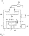
- Fig. 2 illustrates the process station 12 in more detail.
- the process station 12 includes a vacuum chamber 20, a target holder 21 supporting a target 22 of aluminium and a heater 23 which is positioned below a substrate 24 with a conditioned surface 25.
- the process station 12 further comprises nitrogen gas source 26 and an argon gas source 27 from which the process gases may be allowed to flow into the vacuum chamber 20.
- the heater 23 includes a heater element 28 and a substrate facing surface 29 which is spaced at a predetermined distance 30 from the rear side 31 of the substrate 24.
- the substrate 24 may be held at the predetermined distance 30 by means of a height adjustable substrate holder 32 having a ring 33 which is used to support the periphery of the rear side 31 of the substrate 24.
- the substrate 24 is positioned directly opposing the target 22.
- the target 22 is coupled to a DC power supply 34.
- the vacuum chamber 20 is pumped out, the substrate 24 is heated to a process temperature such as 770°C by the heater 23.
- a process temperature such as 770°C by the heater 23.
- the substrate 24 argon process gas may be allowed to flow into the vacuum chamber 20 and the DC power supply is applied to the target 22 so that aluminium is sputtered from the target 22 to form an aluminium film on the conditioned surface 25 of the substrate 24.
- the vacuum chamber 20 is pumped out. After that, the nitrogen and argon process gases are allowed to flow into the vacuum chamber 20 and the DC power supply is applied to the target 22 so that aluminium is sputtered from the target 22, reacts with the nitrogen process gas to form an aluminium nitride layer on the conditioned surface 25 of the substrate 24.
- One exemplary method comprises the single-substrate-treatment of a 6 inch ⁇ 111> silicon substrate in an individual treatment chamber.
- the ⁇ 111> silicon substrate is introduced into a semiconductor manufacturing tool and transferred to a processing station configured to perform an etching step.
- the process environment is pumped down to remove unwanted gases and remains of earlier process steps, for example for 10 s, and in parallel the temperature of substrate is adjusted to a temperature T 2 which may be about 50°C, for example.
- Ar gas is introduced, and the pressure and gas flow allowed to stabilize, for example at a chamber pressure of 5x10 -4 mbar.
- a substrate surface is soft-etched with Ar ions of the RF plasma. Conditions of about 50 W for 10 s -30 s may be used.
- the chamber may be pumped down to clean from used gases before removal of the substrate from etch process station.
- the substrate having a surface conditioned by soft-etching is transferred to a processing station configured to perform an AlN deposition step.
- the process chamber may be a PVD / sputtering chamber equipped with an Al target (300mm diameter) and a pulsed DC power supply.
- the process environment is pumped down to remove unwanted gases and remains of earlier process steps, for example for 10s.
- the substrate is heated up to a temperature T 1 , which may be in the range of 650-800°C, for example 770°C.
- the duration of heat up depends on the heater power and time to stabilize the substrate temperature, and may be 100-600s.
- the cleaned and heated surface is exposed to a hydrogen containing gas, e.g. ammonia.
- an Ar gas flow for example 15 sccm, can be used during heat up.
- the Ar is introduced and, allowed to stabilize, for example for about 5 s.
- a thin aluminium film is deposited while controlling flow of Ar.
- the flow of Ar may be 35 sccm.
- Sputtering may be carried out using DC power of, for example, 100 W for 4 s which may be sufficient for a thin layer with a thickness of around 0.9 nm.
- the process environment is pumped down to remove unwanted gases and remains of this process step, for example for 60s.
- the process gas(es) Ar and N 2 are introduced and, allowed to stabilize, for example for about 10s.
- An AlN layer is deposited while controlling flow of N 2 and Ar.
- the flow of N 2 may 60sccm and the flow of Ar may be 30 sccm.
- Sputtering may be carried out using DC power of, for example, 1.25kW for 470 s which may be sufficient for a layer with a thickness of 100 nm.
- the deposition rate is, therefore, about 0.2 nm/s in this embodiment.
- the process chamber may be pump cleaned from process gas remains.
- the substrate is allowed to cool, over a time period of 10-300s for example, to avoid excessive thermal stress for substrate, limitations of handling equipment and the processed substrate is removed from semiconductor manufacturing tool.
- active cooling before removing the substrate from the processing environment may be performed.
- the temperature decrease may be adjusted to avoid excessive thermal stress on substrate.
- heat up and cool down times are in part dependent on the hardware utilized. They may, depending on respective capabilities, allow for different heat up and cool down times without deviating from the underlying substrate treatment and deposition process.
- the deposition of the AlN layer may be performed by RF sputtering and may be formed by RF sputtering with a variation of the RF power.
- nitridation methods utilize MOCVD and MBE deposition systems, which require the use of nitrogen plasma etching or ammonia exposure at very high temperatures, which are often not suitable for magnetron sputtering.
- nitrogen plasma etching may promote the incorporation of nitrogen by ion bombardment within the silicon substrate and/or the formation of an amorphous oxynitride.
- One limitation of nitridation by ammonia for magnetron sputtering may be that it would complicate the deposition process due to an additional step.
Landscapes
- Chemical & Material Sciences (AREA)
- Engineering & Computer Science (AREA)
- Crystallography & Structural Chemistry (AREA)
- Materials Engineering (AREA)
- Metallurgy (AREA)
- Organic Chemistry (AREA)
- Chemical Kinetics & Catalysis (AREA)
- General Chemical & Material Sciences (AREA)
- Inorganic Chemistry (AREA)
- Physics & Mathematics (AREA)
- General Physics & Mathematics (AREA)
- Condensed Matter Physics & Semiconductors (AREA)
- Manufacturing & Machinery (AREA)
- Computer Hardware Design (AREA)
- Microelectronics & Electronic Packaging (AREA)
- Power Engineering (AREA)
- Physical Vapour Deposition (AREA)
- Drying Of Semiconductors (AREA)
- Plasma & Fusion (AREA)
- Physical Deposition Of Substances That Are Components Of Semiconductor Devices (AREA)
Claims (14)
- Verfahren zum Abscheiden einer Aluminiumnitrid-Schicht auf einem Siliziumsubstrat, umfassend:- Bereitstellen eines Siliziumsubstrats;- Platzieren des Substrats in einer Vakuumkammer;- Konditionieren eine Oberfläche des Substrats durch Ätzen und Herstellen einer konditionierten Oberfläche;- Erwärmen des Substrats auf eine Temperatur T1;- Abscheiden eines Aluminiumfilms auf die konditionierte Oberfläche des Substrats durch ein Sputterverfahren unter einer Argon-Atmosphäre undAbscheiden einer epitaktischen Aluminiumnitrid-Schicht auf dem Aluminiumfilm durch ein Sputterverfahren unter einer Atmosphäre von Stickstoff und Argon, wobei das Konditionieren der Substratoberfläche ein mildes Plasmaätzen der Oberfläche unter Vakuum umfasst, das milde Plasmaätzen ein Erhitzen des Substrats auf eine Temperatur T2, ein Einlassen von Argon in die Vakuumkammer und das Behandeln der Oberfläche des Substrats mit einem Plasma umfasst, wobei T2 < T1, und das milde Plasmaätzen bei einem Druck von 2 * 10-4 mbar bis 8 * 10-4 mbar mit einem RF-Plasma welches Ar+ Ionen umfasst, durchgeführt wird.
- Verfahren nach Anspruch 1, wobei T2 auf 35° C bis 70°C eingestellt ist.
- Verfahren nach Anspruch 1 bis 2, wobei das Bereitstellen des Siliziumubstrats das Bereitstellen eines <111> Siliziumsubstrats umfasst.
- Verfahren nach einem der Ansprüche 1 bis 3, wobei das Ätzen vorzugseise das Entfernen chemisch gebundenen Sauerstoffs vom Substrat umfasst.
- Verfahren nach einem der Ansprüche 1 bis 4, wobei nach dem Abscheiden des Aluminiumfilms die Oberfläche hauptsächlich aluminium-terminiert ist.
- Verfahren nach einem der Ansprüche 1 bis 5, bei dem die konditionierte Oberfläche des Weiteren nach dem Konditionieren in der Vakuumkammer einem wasserstoffhaltigen Gasfluss ausgesetzt wird.
- Verfahren nach einem der Ansprüche 1 bis 6, wobei T1 in einem Bereich von 650°C bis 800°C liegt.
- Verfahren nach einem der Ansprüche 1 bis 7, des Weiteren umfassend das Überströmen des Substrats mit Argongas, während das Substrat auf die Temperatur T1 erhitzt wird.
- Verfahren nach einem der Ansprüche 1 bis 8, wobei die Konditionierung in einer ersten Vakuumkammer und das Abscheiden in einer zweiten Vakuumkammer erfolgt.
- Verfahren nach einem der Ansprüche 1 bis 9, des Weiteren umfassend eine Druckreduzierung in der Vakuumkammer nach der Konditionierung.
- Verfahren nach einem der Ansprüche 1 bis 10, wobei die der Aluminiumnitridfilm auf der konditionierten Oberfläche des Substrats durch reaktives Sputtern abgeschieden und eine Gleichstromleistung von ca. 100 W zum Sputtern des Aluminiumfilms auf die konditionierte Oberfläche verwendet wird.
- Verfahren nach einem der Ansprüche 1 bis 11, wobei die Aluminiumnitridschicht durch reaktives Sputtern auf dem Aluminiumfilm abgeschieden wird.
- Verfahren nach Anspruch 12, wobei eine Gleichstromleistung von ca. 1,0 bis 3 kW zum Sputtern der Aluminiumnitridschicht auf den Aluminiumfilm verwendet wird.
- Verfahren nach einem der Ansprüche 1 bis 13, des Weiteren umfassend ein aktives Kühlen des Substrats nach dem Abscheiden der Aluminiumnitridschicht.
Applications Claiming Priority (2)
| Application Number | Priority Date | Filing Date | Title |
|---|---|---|---|
| US201261695551P | 2012-08-31 | 2012-08-31 | |
| PCT/IB2013/058101 WO2014033649A1 (en) | 2012-08-31 | 2013-08-29 | Method for depositing an aluminium nitride layer |
Publications (2)
| Publication Number | Publication Date |
|---|---|
| EP2890835A1 EP2890835A1 (de) | 2015-07-08 |
| EP2890835B1 true EP2890835B1 (de) | 2021-09-08 |
Family
ID=49382553
Family Applications (1)
| Application Number | Title | Priority Date | Filing Date |
|---|---|---|---|
| EP13777342.0A Active EP2890835B1 (de) | 2012-08-31 | 2013-08-29 | Verfahren zur abscheidung einer aluminiumnitridschicht |
Country Status (7)
| Country | Link |
|---|---|
| US (1) | US9607831B2 (de) |
| EP (1) | EP2890835B1 (de) |
| KR (1) | KR101657915B1 (de) |
| CN (1) | CN104583468A (de) |
| SG (1) | SG11201500330VA (de) |
| TW (1) | TWI601855B (de) |
| WO (1) | WO2014033649A1 (de) |
Families Citing this family (6)
| Publication number | Priority date | Publication date | Assignee | Title |
|---|---|---|---|---|
| CN106328759B (zh) * | 2016-08-24 | 2018-03-02 | 山西潞安太阳能科技有限责任公司 | 一种提高多晶硅双面太阳能电池背面开压的镀膜工艺 |
| US10715099B2 (en) * | 2016-10-28 | 2020-07-14 | Samsung Electro-Mechanics Co., Ltd. | Bulk acoustic wave resonator and method for manufacturing the same |
| CN110534403B (zh) * | 2018-05-25 | 2022-09-16 | 北京北方华创微电子装备有限公司 | 硅衬底上沉积氮化铝薄膜的方法和硅片 |
| CN111005072B (zh) * | 2019-12-27 | 2021-07-02 | 河北工业大学 | 一种可优化表面平整度的氮化铝单晶薄膜制备方法 |
| JP7668806B2 (ja) * | 2020-02-06 | 2025-04-25 | アプライド マテリアルズ インコーポレイテッド | 薄膜堆積中に膜特性を調整するための方法及び装置 |
| CN117512511A (zh) * | 2023-12-01 | 2024-02-06 | 福州大学 | 一种在难熔金属基底上生长AlN缓冲层的方法 |
Family Cites Families (11)
| Publication number | Priority date | Publication date | Assignee | Title |
|---|---|---|---|---|
| KR0170387B1 (ko) * | 1989-10-03 | 1999-03-30 | 제임스 조셉 드롱 | 고주파 반도체 웨이퍼 가공장치 및 방법 |
| US5759360A (en) | 1995-03-13 | 1998-06-02 | Applied Materials, Inc. | Wafer clean sputtering process |
| CA2147198A1 (en) * | 1995-04-18 | 1996-10-19 | Chettypalayam R. Selvakumar | Low temperature ion-beam assisted deposition method for realizing sige/si heterostructures |
| US6255179B1 (en) | 1999-08-04 | 2001-07-03 | International Business Machines Corporation | Plasma etch pre-silicide clean |
| DE10006108A1 (de) * | 2000-02-11 | 2001-08-16 | Wolfgang Richter | Verfahren zur Epitaxie einkristalliner Aluminiumnitrid-Schichten |
| US6391748B1 (en) | 2000-10-03 | 2002-05-21 | Texas Tech University | Method of epitaxial growth of high quality nitride layers on silicon substrates |
| US7091412B2 (en) * | 2002-03-04 | 2006-08-15 | Nanoset, Llc | Magnetically shielded assembly |
| US20060124956A1 (en) * | 2004-12-13 | 2006-06-15 | Hui Peng | Quasi group III-nitride substrates and methods of mass production of the same |
| US8227284B2 (en) * | 2006-08-18 | 2012-07-24 | Showa Denko K.K. | Group-III nitride compound semiconductor light-emitting device, method of manufacturing group-III nitride compound semiconductor light-emitting device, and lamp |
| US20100176369A2 (en) | 2008-04-15 | 2010-07-15 | Mark Oliver | Metalized Silicon Substrate for Indium Gallium Nitride Light-Emitting Diodes |
| US8956761B2 (en) * | 2009-11-30 | 2015-02-17 | Oerlikon Advanced Technologies Ag | Lithium ion battery and method for manufacturing of such battery |
-
2013
- 2013-08-29 EP EP13777342.0A patent/EP2890835B1/de active Active
- 2013-08-29 CN CN201380045033.1A patent/CN104583468A/zh active Pending
- 2013-08-29 KR KR1020157002024A patent/KR101657915B1/ko active Active
- 2013-08-29 SG SG11201500330VA patent/SG11201500330VA/en unknown
- 2013-08-29 WO PCT/IB2013/058101 patent/WO2014033649A1/en not_active Ceased
- 2013-08-30 TW TW102131437A patent/TWI601855B/zh active
-
2015
- 2015-02-27 US US14/633,639 patent/US9607831B2/en active Active
Also Published As
| Publication number | Publication date |
|---|---|
| KR20150023882A (ko) | 2015-03-05 |
| TW201418530A (zh) | 2014-05-16 |
| EP2890835A1 (de) | 2015-07-08 |
| KR101657915B1 (ko) | 2016-09-19 |
| TWI601855B (zh) | 2017-10-11 |
| US9607831B2 (en) | 2017-03-28 |
| US20150179430A1 (en) | 2015-06-25 |
| CN104583468A (zh) | 2015-04-29 |
| SG11201500330VA (en) | 2015-02-27 |
| WO2014033649A1 (en) | 2014-03-06 |
Similar Documents
| Publication | Publication Date | Title |
|---|---|---|
| US9478420B2 (en) | Method for depositing a group III nitride semiconductor film | |
| US9607831B2 (en) | Method for depositing an aluminium nitride layer | |
| US11011676B2 (en) | PVD buffer layers for LED fabrication | |
| CN100361320C (zh) | 含p型掺杂剂的氧化锌膜及其制造方法 | |
| KR100504161B1 (ko) | Ⅲ족 질화물계 화합물 반도체 소자의 제조 방법 | |
| TWI651767B (zh) | 形成應力鬆弛緩衝層的方法 | |
| EP2820173B1 (de) | Substrat für galliumnitrid-auf-diamant wafer abscheidung | |
| KR101687595B1 (ko) | 질화물 반도체층의 성막 방법 및 반도체 장치의 제조 방법 | |
| KR101564251B1 (ko) | 에피텍셜 막 형성방법, 스퍼터링 장치, 반도체 발광소자 제조방법, 반도체 발광소자, 및 조명장치 | |
| WO2011136016A1 (ja) | エピタキシャル膜形成方法、真空処理装置、半導体発光素子の製造方法、半導体発光素子、照明装置 | |
| CN101111945A (zh) | 氮化物半导体元件和氮化物半导体结晶层的生长方法 | |
| US20100248458A1 (en) | Coating apparatus and coating method | |
| TW201413783A (zh) | 碳化矽紋層 | |
| JP6364079B2 (ja) | 少なくとも1つの機能層を有する複合体を生産するための方法、または電子もしくは光電子部品をさらに生産するための方法 | |
| US6911079B2 (en) | Method for reducing the resistivity of p-type II-VI and III-V semiconductors | |
| US20030160264A1 (en) | Hetero-junction semiconductor device and manufacturing method thereof | |
| KR102712496B1 (ko) | 갈륨 산화물 박막의 제조 방법 및 이를 이용한 반도체 소자의 제조 방법 | |
| TWI899939B (zh) | 用於uv led結構的方法及系統 | |
| JP2007103955A (ja) | 窒化物半導体素子および窒化物半導体結晶層の成長方法 |
Legal Events
| Date | Code | Title | Description |
|---|---|---|---|
| PUAI | Public reference made under article 153(3) epc to a published international application that has entered the european phase |
Free format text: ORIGINAL CODE: 0009012 |
|
| 17P | Request for examination filed |
Effective date: 20150331 |
|
| AK | Designated contracting states |
Kind code of ref document: A1 Designated state(s): AL AT BE BG CH CY CZ DE DK EE ES FI FR GB GR HR HU IE IS IT LI LT LU LV MC MK MT NL NO PL PT RO RS SE SI SK SM TR |
|
| AX | Request for extension of the european patent |
Extension state: BA ME |
|
| DAX | Request for extension of the european patent (deleted) | ||
| RAP1 | Party data changed (applicant data changed or rights of an application transferred) |
Owner name: EVATEC AG |
|
| STAA | Information on the status of an ep patent application or granted ep patent |
Free format text: STATUS: EXAMINATION IS IN PROGRESS |
|
| 17Q | First examination report despatched |
Effective date: 20170920 |
|
| REG | Reference to a national code |
Ref country code: DE Ref legal event code: R079 Ref document number: 602013079187 Country of ref document: DE Free format text: PREVIOUS MAIN CLASS: C30B0023020000 Ipc: C30B0025060000 |
|
| GRAP | Despatch of communication of intention to grant a patent |
Free format text: ORIGINAL CODE: EPIDOSNIGR1 |
|
| RIC1 | Information provided on ipc code assigned before grant |
Ipc: C30B 25/18 20060101ALI20210315BHEP Ipc: H01L 21/02 20060101ALI20210315BHEP Ipc: C30B 29/40 20060101ALI20210315BHEP Ipc: C30B 25/06 20060101AFI20210315BHEP |
|
| STAA | Information on the status of an ep patent application or granted ep patent |
Free format text: STATUS: GRANT OF PATENT IS INTENDED |
|
| INTG | Intention to grant announced |
Effective date: 20210422 |
|
| GRAS | Grant fee paid |
Free format text: ORIGINAL CODE: EPIDOSNIGR3 |
|
| GRAA | (expected) grant |
Free format text: ORIGINAL CODE: 0009210 |
|
| STAA | Information on the status of an ep patent application or granted ep patent |
Free format text: STATUS: THE PATENT HAS BEEN GRANTED |
|
| AK | Designated contracting states |
Kind code of ref document: B1 Designated state(s): AL AT BE BG CH CY CZ DE DK EE ES FI FR GB GR HR HU IE IS IT LI LT LU LV MC MK MT NL NO PL PT RO RS SE SI SK SM TR |
|
| REG | Reference to a national code |
Ref country code: GB Ref legal event code: FG4D |
|
| REG | Reference to a national code |
Ref country code: AT Ref legal event code: REF Ref document number: 1428675 Country of ref document: AT Kind code of ref document: T Effective date: 20210915 Ref country code: CH Ref legal event code: EP |
|
| REG | Reference to a national code |
Ref country code: IE Ref legal event code: FG4D |
|
| REG | Reference to a national code |
Ref country code: DE Ref legal event code: R096 Ref document number: 602013079187 Country of ref document: DE |
|
| REG | Reference to a national code |
Ref country code: LT Ref legal event code: MG9D |
|
| REG | Reference to a national code |
Ref country code: NL Ref legal event code: MP Effective date: 20210908 |
|
| PG25 | Lapsed in a contracting state [announced via postgrant information from national office to epo] |
Ref country code: LT Free format text: LAPSE BECAUSE OF FAILURE TO SUBMIT A TRANSLATION OF THE DESCRIPTION OR TO PAY THE FEE WITHIN THE PRESCRIBED TIME-LIMIT Effective date: 20210908 Ref country code: BG Free format text: LAPSE BECAUSE OF FAILURE TO SUBMIT A TRANSLATION OF THE DESCRIPTION OR TO PAY THE FEE WITHIN THE PRESCRIBED TIME-LIMIT Effective date: 20211208 Ref country code: NO Free format text: LAPSE BECAUSE OF FAILURE TO SUBMIT A TRANSLATION OF THE DESCRIPTION OR TO PAY THE FEE WITHIN THE PRESCRIBED TIME-LIMIT Effective date: 20211208 Ref country code: RS Free format text: LAPSE BECAUSE OF FAILURE TO SUBMIT A TRANSLATION OF THE DESCRIPTION OR TO PAY THE FEE WITHIN THE PRESCRIBED TIME-LIMIT Effective date: 20210908 Ref country code: FI Free format text: LAPSE BECAUSE OF FAILURE TO SUBMIT A TRANSLATION OF THE DESCRIPTION OR TO PAY THE FEE WITHIN THE PRESCRIBED TIME-LIMIT Effective date: 20210908 Ref country code: ES Free format text: LAPSE BECAUSE OF FAILURE TO SUBMIT A TRANSLATION OF THE DESCRIPTION OR TO PAY THE FEE WITHIN THE PRESCRIBED TIME-LIMIT Effective date: 20210908 Ref country code: SE Free format text: LAPSE BECAUSE OF FAILURE TO SUBMIT A TRANSLATION OF THE DESCRIPTION OR TO PAY THE FEE WITHIN THE PRESCRIBED TIME-LIMIT Effective date: 20210908 Ref country code: HR Free format text: LAPSE BECAUSE OF FAILURE TO SUBMIT A TRANSLATION OF THE DESCRIPTION OR TO PAY THE FEE WITHIN THE PRESCRIBED TIME-LIMIT Effective date: 20210908 |
|
| REG | Reference to a national code |
Ref country code: AT Ref legal event code: MK05 Ref document number: 1428675 Country of ref document: AT Kind code of ref document: T Effective date: 20210908 |
|
| PG25 | Lapsed in a contracting state [announced via postgrant information from national office to epo] |
Ref country code: LV Free format text: LAPSE BECAUSE OF FAILURE TO SUBMIT A TRANSLATION OF THE DESCRIPTION OR TO PAY THE FEE WITHIN THE PRESCRIBED TIME-LIMIT Effective date: 20210908 Ref country code: GR Free format text: LAPSE BECAUSE OF FAILURE TO SUBMIT A TRANSLATION OF THE DESCRIPTION OR TO PAY THE FEE WITHIN THE PRESCRIBED TIME-LIMIT Effective date: 20211209 |
|
| PG25 | Lapsed in a contracting state [announced via postgrant information from national office to epo] |
Ref country code: AT Free format text: LAPSE BECAUSE OF FAILURE TO SUBMIT A TRANSLATION OF THE DESCRIPTION OR TO PAY THE FEE WITHIN THE PRESCRIBED TIME-LIMIT Effective date: 20210908 |
|
| PG25 | Lapsed in a contracting state [announced via postgrant information from national office to epo] |
Ref country code: IS Free format text: LAPSE BECAUSE OF FAILURE TO SUBMIT A TRANSLATION OF THE DESCRIPTION OR TO PAY THE FEE WITHIN THE PRESCRIBED TIME-LIMIT Effective date: 20220108 Ref country code: SM Free format text: LAPSE BECAUSE OF FAILURE TO SUBMIT A TRANSLATION OF THE DESCRIPTION OR TO PAY THE FEE WITHIN THE PRESCRIBED TIME-LIMIT Effective date: 20210908 Ref country code: SK Free format text: LAPSE BECAUSE OF FAILURE TO SUBMIT A TRANSLATION OF THE DESCRIPTION OR TO PAY THE FEE WITHIN THE PRESCRIBED TIME-LIMIT Effective date: 20210908 Ref country code: RO Free format text: LAPSE BECAUSE OF FAILURE TO SUBMIT A TRANSLATION OF THE DESCRIPTION OR TO PAY THE FEE WITHIN THE PRESCRIBED TIME-LIMIT Effective date: 20210908 Ref country code: PT Free format text: LAPSE BECAUSE OF FAILURE TO SUBMIT A TRANSLATION OF THE DESCRIPTION OR TO PAY THE FEE WITHIN THE PRESCRIBED TIME-LIMIT Effective date: 20220110 Ref country code: PL Free format text: LAPSE BECAUSE OF FAILURE TO SUBMIT A TRANSLATION OF THE DESCRIPTION OR TO PAY THE FEE WITHIN THE PRESCRIBED TIME-LIMIT Effective date: 20210908 Ref country code: NL Free format text: LAPSE BECAUSE OF FAILURE TO SUBMIT A TRANSLATION OF THE DESCRIPTION OR TO PAY THE FEE WITHIN THE PRESCRIBED TIME-LIMIT Effective date: 20210908 Ref country code: EE Free format text: LAPSE BECAUSE OF FAILURE TO SUBMIT A TRANSLATION OF THE DESCRIPTION OR TO PAY THE FEE WITHIN THE PRESCRIBED TIME-LIMIT Effective date: 20210908 Ref country code: CZ Free format text: LAPSE BECAUSE OF FAILURE TO SUBMIT A TRANSLATION OF THE DESCRIPTION OR TO PAY THE FEE WITHIN THE PRESCRIBED TIME-LIMIT Effective date: 20210908 Ref country code: AL Free format text: LAPSE BECAUSE OF FAILURE TO SUBMIT A TRANSLATION OF THE DESCRIPTION OR TO PAY THE FEE WITHIN THE PRESCRIBED TIME-LIMIT Effective date: 20210908 |
|
| REG | Reference to a national code |
Ref country code: DE Ref legal event code: R097 Ref document number: 602013079187 Country of ref document: DE |
|
| PLBE | No opposition filed within time limit |
Free format text: ORIGINAL CODE: 0009261 |
|
| STAA | Information on the status of an ep patent application or granted ep patent |
Free format text: STATUS: NO OPPOSITION FILED WITHIN TIME LIMIT |
|
| PG25 | Lapsed in a contracting state [announced via postgrant information from national office to epo] |
Ref country code: DK Free format text: LAPSE BECAUSE OF FAILURE TO SUBMIT A TRANSLATION OF THE DESCRIPTION OR TO PAY THE FEE WITHIN THE PRESCRIBED TIME-LIMIT Effective date: 20210908 |
|
| 26N | No opposition filed |
Effective date: 20220609 |
|
| PG25 | Lapsed in a contracting state [announced via postgrant information from national office to epo] |
Ref country code: SI Free format text: LAPSE BECAUSE OF FAILURE TO SUBMIT A TRANSLATION OF THE DESCRIPTION OR TO PAY THE FEE WITHIN THE PRESCRIBED TIME-LIMIT Effective date: 20210908 |
|
| PG25 | Lapsed in a contracting state [announced via postgrant information from national office to epo] |
Ref country code: IT Free format text: LAPSE BECAUSE OF FAILURE TO SUBMIT A TRANSLATION OF THE DESCRIPTION OR TO PAY THE FEE WITHIN THE PRESCRIBED TIME-LIMIT Effective date: 20210908 |
|
| REG | Reference to a national code |
Ref country code: DE Ref legal event code: R082 Ref document number: 602013079187 Country of ref document: DE Representative=s name: SKM-IP SCHMID KRAUSS KUTTENKEULER MALESCHA SCH, DE |
|
| PG25 | Lapsed in a contracting state [announced via postgrant information from national office to epo] |
Ref country code: MC Free format text: LAPSE BECAUSE OF FAILURE TO SUBMIT A TRANSLATION OF THE DESCRIPTION OR TO PAY THE FEE WITHIN THE PRESCRIBED TIME-LIMIT Effective date: 20210908 |
|
| REG | Reference to a national code |
Ref country code: CH Ref legal event code: PL |
|
| GBPC | Gb: european patent ceased through non-payment of renewal fee |
Effective date: 20220829 |
|
| PG25 | Lapsed in a contracting state [announced via postgrant information from national office to epo] |
Ref country code: LU Free format text: LAPSE BECAUSE OF NON-PAYMENT OF DUE FEES Effective date: 20220829 Ref country code: LI Free format text: LAPSE BECAUSE OF NON-PAYMENT OF DUE FEES Effective date: 20220831 Ref country code: CH Free format text: LAPSE BECAUSE OF NON-PAYMENT OF DUE FEES Effective date: 20220831 |
|
| REG | Reference to a national code |
Ref country code: BE Ref legal event code: MM Effective date: 20220831 |
|
| P01 | Opt-out of the competence of the unified patent court (upc) registered |
Effective date: 20230526 |
|
| PG25 | Lapsed in a contracting state [announced via postgrant information from national office to epo] |
Ref country code: IE Free format text: LAPSE BECAUSE OF NON-PAYMENT OF DUE FEES Effective date: 20220829 Ref country code: FR Free format text: LAPSE BECAUSE OF NON-PAYMENT OF DUE FEES Effective date: 20220831 |
|
| PG25 | Lapsed in a contracting state [announced via postgrant information from national office to epo] |
Ref country code: BE Free format text: LAPSE BECAUSE OF NON-PAYMENT OF DUE FEES Effective date: 20220831 |
|
| PG25 | Lapsed in a contracting state [announced via postgrant information from national office to epo] |
Ref country code: GB Free format text: LAPSE BECAUSE OF NON-PAYMENT OF DUE FEES Effective date: 20220829 |
|
| PG25 | Lapsed in a contracting state [announced via postgrant information from national office to epo] |
Ref country code: HU Free format text: LAPSE BECAUSE OF FAILURE TO SUBMIT A TRANSLATION OF THE DESCRIPTION OR TO PAY THE FEE WITHIN THE PRESCRIBED TIME-LIMIT; INVALID AB INITIO Effective date: 20130829 |
|
| PG25 | Lapsed in a contracting state [announced via postgrant information from national office to epo] |
Ref country code: CY Free format text: LAPSE BECAUSE OF FAILURE TO SUBMIT A TRANSLATION OF THE DESCRIPTION OR TO PAY THE FEE WITHIN THE PRESCRIBED TIME-LIMIT Effective date: 20210908 |
|
| PG25 | Lapsed in a contracting state [announced via postgrant information from national office to epo] |
Ref country code: MK Free format text: LAPSE BECAUSE OF FAILURE TO SUBMIT A TRANSLATION OF THE DESCRIPTION OR TO PAY THE FEE WITHIN THE PRESCRIBED TIME-LIMIT Effective date: 20210908 |
|
| PG25 | Lapsed in a contracting state [announced via postgrant information from national office to epo] |
Ref country code: MT Free format text: LAPSE BECAUSE OF FAILURE TO SUBMIT A TRANSLATION OF THE DESCRIPTION OR TO PAY THE FEE WITHIN THE PRESCRIBED TIME-LIMIT Effective date: 20210908 |
|
| PGFP | Annual fee paid to national office [announced via postgrant information from national office to epo] |
Ref country code: DE Payment date: 20250801 Year of fee payment: 13 |
|
| PG25 | Lapsed in a contracting state [announced via postgrant information from national office to epo] |
Ref country code: TR Free format text: LAPSE BECAUSE OF FAILURE TO SUBMIT A TRANSLATION OF THE DESCRIPTION OR TO PAY THE FEE WITHIN THE PRESCRIBED TIME-LIMIT Effective date: 20210908 |