EP2889902A1 - Electric power semiconductor device - Google Patents
Electric power semiconductor device Download PDFInfo
- Publication number
- EP2889902A1 EP2889902A1 EP13832786.1A EP13832786A EP2889902A1 EP 2889902 A1 EP2889902 A1 EP 2889902A1 EP 13832786 A EP13832786 A EP 13832786A EP 2889902 A1 EP2889902 A1 EP 2889902A1
- Authority
- EP
- European Patent Office
- Prior art keywords
- electric power
- power semiconductor
- electrode
- bonding
- semiconductor device
- Prior art date
- Legal status (The legal status is an assumption and is not a legal conclusion. Google has not performed a legal analysis and makes no representation as to the accuracy of the status listed.)
- Granted
Links
Images

Classifications
-
- H—ELECTRICITY
- H05—ELECTRIC TECHNIQUES NOT OTHERWISE PROVIDED FOR
- H05K—PRINTED CIRCUITS; CASINGS OR CONSTRUCTIONAL DETAILS OF ELECTRIC APPARATUS; MANUFACTURE OF ASSEMBLAGES OF ELECTRICAL COMPONENTS
- H05K1/00—Printed circuits
- H05K1/02—Details
- H05K1/0201—Thermal arrangements, e.g. for cooling, heating or preventing overheating
- H05K1/0203—Cooling of mounted components
-
- H—ELECTRICITY
- H10—SEMICONDUCTOR DEVICES; ELECTRIC SOLID-STATE DEVICES NOT OTHERWISE PROVIDED FOR
- H10W—GENERIC PACKAGES, INTERCONNECTIONS, CONNECTORS OR OTHER CONSTRUCTIONAL DETAILS OF DEVICES COVERED BY CLASS H10
- H10W40/00—Arrangements for thermal protection or thermal control
- H10W40/10—Arrangements for heating
-
- H—ELECTRICITY
- H10—SEMICONDUCTOR DEVICES; ELECTRIC SOLID-STATE DEVICES NOT OTHERWISE PROVIDED FOR
- H10W—GENERIC PACKAGES, INTERCONNECTIONS, CONNECTORS OR OTHER CONSTRUCTIONAL DETAILS OF DEVICES COVERED BY CLASS H10
- H10W40/00—Arrangements for thermal protection or thermal control
- H10W40/20—Arrangements for cooling
- H10W40/25—Arrangements for cooling characterised by their materials
- H10W40/255—Arrangements for cooling characterised by their materials having a laminate or multilayered structure, e.g. direct bond copper [DBC] ceramic substrates
-
- H—ELECTRICITY
- H10—SEMICONDUCTOR DEVICES; ELECTRIC SOLID-STATE DEVICES NOT OTHERWISE PROVIDED FOR
- H10W—GENERIC PACKAGES, INTERCONNECTIONS, CONNECTORS OR OTHER CONSTRUCTIONAL DETAILS OF DEVICES COVERED BY CLASS H10
- H10W70/00—Package substrates; Interposers; Redistribution layers [RDL]
- H10W70/20—Conductive package substrates serving as an interconnection, e.g. metal plates
-
- H—ELECTRICITY
- H10—SEMICONDUCTOR DEVICES; ELECTRIC SOLID-STATE DEVICES NOT OTHERWISE PROVIDED FOR
- H10W—GENERIC PACKAGES, INTERCONNECTIONS, CONNECTORS OR OTHER CONSTRUCTIONAL DETAILS OF DEVICES COVERED BY CLASS H10
- H10W70/00—Package substrates; Interposers; Redistribution layers [RDL]
- H10W70/60—Insulating or insulated package substrates; Interposers; Redistribution layers
- H10W70/67—Insulating or insulated package substrates; Interposers; Redistribution layers characterised by their insulating layers or insulating parts
- H10W70/68—Shapes or dispositions thereof
-
- H—ELECTRICITY
- H10—SEMICONDUCTOR DEVICES; ELECTRIC SOLID-STATE DEVICES NOT OTHERWISE PROVIDED FOR
- H10W—GENERIC PACKAGES, INTERCONNECTIONS, CONNECTORS OR OTHER CONSTRUCTIONAL DETAILS OF DEVICES COVERED BY CLASS H10
- H10W72/00—Interconnections or connectors in packages
- H10W72/071—Connecting or disconnecting
- H10W72/073—Connecting or disconnecting of die-attach connectors
-
- H—ELECTRICITY
- H10—SEMICONDUCTOR DEVICES; ELECTRIC SOLID-STATE DEVICES NOT OTHERWISE PROVIDED FOR
- H10W—GENERIC PACKAGES, INTERCONNECTIONS, CONNECTORS OR OTHER CONSTRUCTIONAL DETAILS OF DEVICES COVERED BY CLASS H10
- H10W72/00—Interconnections or connectors in packages
- H10W72/071—Connecting or disconnecting
- H10W72/075—Connecting or disconnecting of bond wires
-
- H—ELECTRICITY
- H10—SEMICONDUCTOR DEVICES; ELECTRIC SOLID-STATE DEVICES NOT OTHERWISE PROVIDED FOR
- H10W—GENERIC PACKAGES, INTERCONNECTIONS, CONNECTORS OR OTHER CONSTRUCTIONAL DETAILS OF DEVICES COVERED BY CLASS H10
- H10W72/00—Interconnections or connectors in packages
- H10W72/30—Die-attach connectors
-
- H—ELECTRICITY
- H10—SEMICONDUCTOR DEVICES; ELECTRIC SOLID-STATE DEVICES NOT OTHERWISE PROVIDED FOR
- H10W—GENERIC PACKAGES, INTERCONNECTIONS, CONNECTORS OR OTHER CONSTRUCTIONAL DETAILS OF DEVICES COVERED BY CLASS H10
- H10W72/00—Interconnections or connectors in packages
- H10W72/50—Bond wires
-
- H—ELECTRICITY
- H10—SEMICONDUCTOR DEVICES; ELECTRIC SOLID-STATE DEVICES NOT OTHERWISE PROVIDED FOR
- H10W—GENERIC PACKAGES, INTERCONNECTIONS, CONNECTORS OR OTHER CONSTRUCTIONAL DETAILS OF DEVICES COVERED BY CLASS H10
- H10W72/00—Interconnections or connectors in packages
- H10W72/851—Dispositions of multiple connectors or interconnections
-
- H—ELECTRICITY
- H10—SEMICONDUCTOR DEVICES; ELECTRIC SOLID-STATE DEVICES NOT OTHERWISE PROVIDED FOR
- H10W—GENERIC PACKAGES, INTERCONNECTIONS, CONNECTORS OR OTHER CONSTRUCTIONAL DETAILS OF DEVICES COVERED BY CLASS H10
- H10W72/00—Interconnections or connectors in packages
- H10W72/90—Bond pads, in general
-
- H—ELECTRICITY
- H10—SEMICONDUCTOR DEVICES; ELECTRIC SOLID-STATE DEVICES NOT OTHERWISE PROVIDED FOR
- H10W—GENERIC PACKAGES, INTERCONNECTIONS, CONNECTORS OR OTHER CONSTRUCTIONAL DETAILS OF DEVICES COVERED BY CLASS H10
- H10W90/00—Package configurations
-
- H—ELECTRICITY
- H10—SEMICONDUCTOR DEVICES; ELECTRIC SOLID-STATE DEVICES NOT OTHERWISE PROVIDED FOR
- H10W—GENERIC PACKAGES, INTERCONNECTIONS, CONNECTORS OR OTHER CONSTRUCTIONAL DETAILS OF DEVICES COVERED BY CLASS H10
- H10W99/00—Subject matter not provided for in other groups of this subclass
-
- H—ELECTRICITY
- H10—SEMICONDUCTOR DEVICES; ELECTRIC SOLID-STATE DEVICES NOT OTHERWISE PROVIDED FOR
- H10W—GENERIC PACKAGES, INTERCONNECTIONS, CONNECTORS OR OTHER CONSTRUCTIONAL DETAILS OF DEVICES COVERED BY CLASS H10
- H10W72/00—Interconnections or connectors in packages
- H10W72/071—Connecting or disconnecting
- H10W72/073—Connecting or disconnecting of die-attach connectors
- H10W72/07331—Connecting techniques
- H10W72/07336—Soldering or alloying
-
- H—ELECTRICITY
- H10—SEMICONDUCTOR DEVICES; ELECTRIC SOLID-STATE DEVICES NOT OTHERWISE PROVIDED FOR
- H10W—GENERIC PACKAGES, INTERCONNECTIONS, CONNECTORS OR OTHER CONSTRUCTIONAL DETAILS OF DEVICES COVERED BY CLASS H10
- H10W72/00—Interconnections or connectors in packages
- H10W72/071—Connecting or disconnecting
- H10W72/075—Connecting or disconnecting of bond wires
- H10W72/07531—Techniques
- H10W72/07532—Compression bonding, e.g. thermocompression bonding
- H10W72/07533—Ultrasonic bonding, e.g. thermosonic bonding
-
- H—ELECTRICITY
- H10—SEMICONDUCTOR DEVICES; ELECTRIC SOLID-STATE DEVICES NOT OTHERWISE PROVIDED FOR
- H10W—GENERIC PACKAGES, INTERCONNECTIONS, CONNECTORS OR OTHER CONSTRUCTIONAL DETAILS OF DEVICES COVERED BY CLASS H10
- H10W72/00—Interconnections or connectors in packages
- H10W72/071—Connecting or disconnecting
- H10W72/076—Connecting or disconnecting of strap connectors
-
- H—ELECTRICITY
- H10—SEMICONDUCTOR DEVICES; ELECTRIC SOLID-STATE DEVICES NOT OTHERWISE PROVIDED FOR
- H10W—GENERIC PACKAGES, INTERCONNECTIONS, CONNECTORS OR OTHER CONSTRUCTIONAL DETAILS OF DEVICES COVERED BY CLASS H10
- H10W72/00—Interconnections or connectors in packages
- H10W72/071—Connecting or disconnecting
- H10W72/076—Connecting or disconnecting of strap connectors
- H10W72/07631—Techniques
- H10W72/07636—Soldering or alloying
-
- H—ELECTRICITY
- H10—SEMICONDUCTOR DEVICES; ELECTRIC SOLID-STATE DEVICES NOT OTHERWISE PROVIDED FOR
- H10W—GENERIC PACKAGES, INTERCONNECTIONS, CONNECTORS OR OTHER CONSTRUCTIONAL DETAILS OF DEVICES COVERED BY CLASS H10
- H10W72/00—Interconnections or connectors in packages
- H10W72/071—Connecting or disconnecting
- H10W72/076—Connecting or disconnecting of strap connectors
- H10W72/07651—Connecting or disconnecting of strap connectors characterised by changes in properties of the strap connectors during connecting
- H10W72/07653—Connecting or disconnecting of strap connectors characterised by changes in properties of the strap connectors during connecting changes in shapes
-
- H—ELECTRICITY
- H10—SEMICONDUCTOR DEVICES; ELECTRIC SOLID-STATE DEVICES NOT OTHERWISE PROVIDED FOR
- H10W—GENERIC PACKAGES, INTERCONNECTIONS, CONNECTORS OR OTHER CONSTRUCTIONAL DETAILS OF DEVICES COVERED BY CLASS H10
- H10W72/00—Interconnections or connectors in packages
- H10W72/071—Connecting or disconnecting
- H10W72/076—Connecting or disconnecting of strap connectors
- H10W72/07651—Connecting or disconnecting of strap connectors characterised by changes in properties of the strap connectors during connecting
- H10W72/07654—Connecting or disconnecting of strap connectors characterised by changes in properties of the strap connectors during connecting changes in dispositions
-
- H—ELECTRICITY
- H10—SEMICONDUCTOR DEVICES; ELECTRIC SOLID-STATE DEVICES NOT OTHERWISE PROVIDED FOR
- H10W—GENERIC PACKAGES, INTERCONNECTIONS, CONNECTORS OR OTHER CONSTRUCTIONAL DETAILS OF DEVICES COVERED BY CLASS H10
- H10W72/00—Interconnections or connectors in packages
- H10W72/30—Die-attach connectors
- H10W72/351—Materials of die-attach connectors
- H10W72/352—Materials of die-attach connectors comprising metals or metalloids, e.g. solders
-
- H—ELECTRICITY
- H10—SEMICONDUCTOR DEVICES; ELECTRIC SOLID-STATE DEVICES NOT OTHERWISE PROVIDED FOR
- H10W—GENERIC PACKAGES, INTERCONNECTIONS, CONNECTORS OR OTHER CONSTRUCTIONAL DETAILS OF DEVICES COVERED BY CLASS H10
- H10W72/00—Interconnections or connectors in packages
- H10W72/50—Bond wires
- H10W72/531—Shapes of wire connectors
- H10W72/5363—Shapes of wire connectors the connected ends being wedge-shaped
-
- H—ELECTRICITY
- H10—SEMICONDUCTOR DEVICES; ELECTRIC SOLID-STATE DEVICES NOT OTHERWISE PROVIDED FOR
- H10W—GENERIC PACKAGES, INTERCONNECTIONS, CONNECTORS OR OTHER CONSTRUCTIONAL DETAILS OF DEVICES COVERED BY CLASS H10
- H10W72/00—Interconnections or connectors in packages
- H10W72/50—Bond wires
- H10W72/541—Dispositions of bond wires
- H10W72/5445—Dispositions of bond wires being orthogonal to a side surface of the chip, e.g. parallel arrangements
-
- H—ELECTRICITY
- H10—SEMICONDUCTOR DEVICES; ELECTRIC SOLID-STATE DEVICES NOT OTHERWISE PROVIDED FOR
- H10W—GENERIC PACKAGES, INTERCONNECTIONS, CONNECTORS OR OTHER CONSTRUCTIONAL DETAILS OF DEVICES COVERED BY CLASS H10
- H10W72/00—Interconnections or connectors in packages
- H10W72/50—Bond wires
- H10W72/551—Materials of bond wires
- H10W72/552—Materials of bond wires comprising metals or metalloids, e.g. silver
- H10W72/5522—Materials of bond wires comprising metals or metalloids, e.g. silver comprising gold [Au]
-
- H—ELECTRICITY
- H10—SEMICONDUCTOR DEVICES; ELECTRIC SOLID-STATE DEVICES NOT OTHERWISE PROVIDED FOR
- H10W—GENERIC PACKAGES, INTERCONNECTIONS, CONNECTORS OR OTHER CONSTRUCTIONAL DETAILS OF DEVICES COVERED BY CLASS H10
- H10W72/00—Interconnections or connectors in packages
- H10W72/50—Bond wires
- H10W72/551—Materials of bond wires
- H10W72/552—Materials of bond wires comprising metals or metalloids, e.g. silver
- H10W72/5524—Materials of bond wires comprising metals or metalloids, e.g. silver comprising aluminium [Al]
-
- H—ELECTRICITY
- H10—SEMICONDUCTOR DEVICES; ELECTRIC SOLID-STATE DEVICES NOT OTHERWISE PROVIDED FOR
- H10W—GENERIC PACKAGES, INTERCONNECTIONS, CONNECTORS OR OTHER CONSTRUCTIONAL DETAILS OF DEVICES COVERED BY CLASS H10
- H10W72/00—Interconnections or connectors in packages
- H10W72/50—Bond wires
- H10W72/551—Materials of bond wires
- H10W72/552—Materials of bond wires comprising metals or metalloids, e.g. silver
- H10W72/5525—Materials of bond wires comprising metals or metalloids, e.g. silver comprising copper [Cu]
-
- H—ELECTRICITY
- H10—SEMICONDUCTOR DEVICES; ELECTRIC SOLID-STATE DEVICES NOT OTHERWISE PROVIDED FOR
- H10W—GENERIC PACKAGES, INTERCONNECTIONS, CONNECTORS OR OTHER CONSTRUCTIONAL DETAILS OF DEVICES COVERED BY CLASS H10
- H10W72/00—Interconnections or connectors in packages
- H10W72/50—Bond wires
- H10W72/59—Bond pads specially adapted therefor
-
- H—ELECTRICITY
- H10—SEMICONDUCTOR DEVICES; ELECTRIC SOLID-STATE DEVICES NOT OTHERWISE PROVIDED FOR
- H10W—GENERIC PACKAGES, INTERCONNECTIONS, CONNECTORS OR OTHER CONSTRUCTIONAL DETAILS OF DEVICES COVERED BY CLASS H10
- H10W72/00—Interconnections or connectors in packages
- H10W72/60—Strap connectors, e.g. thick copper clips for grounding of power devices
- H10W72/631—Shapes of strap connectors
-
- H—ELECTRICITY
- H10—SEMICONDUCTOR DEVICES; ELECTRIC SOLID-STATE DEVICES NOT OTHERWISE PROVIDED FOR
- H10W—GENERIC PACKAGES, INTERCONNECTIONS, CONNECTORS OR OTHER CONSTRUCTIONAL DETAILS OF DEVICES COVERED BY CLASS H10
- H10W72/00—Interconnections or connectors in packages
- H10W72/60—Strap connectors, e.g. thick copper clips for grounding of power devices
- H10W72/631—Shapes of strap connectors
- H10W72/634—Cross-sectional shape
-
- H—ELECTRICITY
- H10—SEMICONDUCTOR DEVICES; ELECTRIC SOLID-STATE DEVICES NOT OTHERWISE PROVIDED FOR
- H10W—GENERIC PACKAGES, INTERCONNECTIONS, CONNECTORS OR OTHER CONSTRUCTIONAL DETAILS OF DEVICES COVERED BY CLASS H10
- H10W72/00—Interconnections or connectors in packages
- H10W72/60—Strap connectors, e.g. thick copper clips for grounding of power devices
- H10W72/641—Dispositions of strap connectors
- H10W72/647—Dispositions of multiple strap connectors
-
- H—ELECTRICITY
- H10—SEMICONDUCTOR DEVICES; ELECTRIC SOLID-STATE DEVICES NOT OTHERWISE PROVIDED FOR
- H10W—GENERIC PACKAGES, INTERCONNECTIONS, CONNECTORS OR OTHER CONSTRUCTIONAL DETAILS OF DEVICES COVERED BY CLASS H10
- H10W72/00—Interconnections or connectors in packages
- H10W72/60—Strap connectors, e.g. thick copper clips for grounding of power devices
- H10W72/651—Materials of strap connectors
- H10W72/652—Materials of strap connectors comprising metals or metalloids, e.g. silver
-
- H—ELECTRICITY
- H10—SEMICONDUCTOR DEVICES; ELECTRIC SOLID-STATE DEVICES NOT OTHERWISE PROVIDED FOR
- H10W—GENERIC PACKAGES, INTERCONNECTIONS, CONNECTORS OR OTHER CONSTRUCTIONAL DETAILS OF DEVICES COVERED BY CLASS H10
- H10W72/00—Interconnections or connectors in packages
- H10W72/60—Strap connectors, e.g. thick copper clips for grounding of power devices
- H10W72/691—Bond pads specially adapted therefor
-
- H—ELECTRICITY
- H10—SEMICONDUCTOR DEVICES; ELECTRIC SOLID-STATE DEVICES NOT OTHERWISE PROVIDED FOR
- H10W—GENERIC PACKAGES, INTERCONNECTIONS, CONNECTORS OR OTHER CONSTRUCTIONAL DETAILS OF DEVICES COVERED BY CLASS H10
- H10W72/00—Interconnections or connectors in packages
- H10W72/851—Dispositions of multiple connectors or interconnections
- H10W72/874—On different surfaces
- H10W72/884—Die-attach connectors and bond wires
-
- H—ELECTRICITY
- H10—SEMICONDUCTOR DEVICES; ELECTRIC SOLID-STATE DEVICES NOT OTHERWISE PROVIDED FOR
- H10W—GENERIC PACKAGES, INTERCONNECTIONS, CONNECTORS OR OTHER CONSTRUCTIONAL DETAILS OF DEVICES COVERED BY CLASS H10
- H10W72/00—Interconnections or connectors in packages
- H10W72/851—Dispositions of multiple connectors or interconnections
- H10W72/874—On different surfaces
- H10W72/886—Die-attach connectors and strap connectors
-
- H—ELECTRICITY
- H10—SEMICONDUCTOR DEVICES; ELECTRIC SOLID-STATE DEVICES NOT OTHERWISE PROVIDED FOR
- H10W—GENERIC PACKAGES, INTERCONNECTIONS, CONNECTORS OR OTHER CONSTRUCTIONAL DETAILS OF DEVICES COVERED BY CLASS H10
- H10W72/00—Interconnections or connectors in packages
- H10W72/90—Bond pads, in general
- H10W72/921—Structures or relative sizes of bond pads
- H10W72/926—Multiple bond pads having different sizes
-
- H—ELECTRICITY
- H10—SEMICONDUCTOR DEVICES; ELECTRIC SOLID-STATE DEVICES NOT OTHERWISE PROVIDED FOR
- H10W—GENERIC PACKAGES, INTERCONNECTIONS, CONNECTORS OR OTHER CONSTRUCTIONAL DETAILS OF DEVICES COVERED BY CLASS H10
- H10W72/00—Interconnections or connectors in packages
- H10W72/90—Bond pads, in general
- H10W72/941—Dispositions of bond pads
- H10W72/944—Dispositions of multiple bond pads
-
- H—ELECTRICITY
- H10—SEMICONDUCTOR DEVICES; ELECTRIC SOLID-STATE DEVICES NOT OTHERWISE PROVIDED FOR
- H10W—GENERIC PACKAGES, INTERCONNECTIONS, CONNECTORS OR OTHER CONSTRUCTIONAL DETAILS OF DEVICES COVERED BY CLASS H10
- H10W72/00—Interconnections or connectors in packages
- H10W72/90—Bond pads, in general
- H10W72/951—Materials of bond pads
- H10W72/952—Materials of bond pads comprising metals or metalloids, e.g. PbSn, Ag or Cu
-
- H—ELECTRICITY
- H10—SEMICONDUCTOR DEVICES; ELECTRIC SOLID-STATE DEVICES NOT OTHERWISE PROVIDED FOR
- H10W—GENERIC PACKAGES, INTERCONNECTIONS, CONNECTORS OR OTHER CONSTRUCTIONAL DETAILS OF DEVICES COVERED BY CLASS H10
- H10W74/00—Encapsulations, e.g. protective coatings
-
- H—ELECTRICITY
- H10—SEMICONDUCTOR DEVICES; ELECTRIC SOLID-STATE DEVICES NOT OTHERWISE PROVIDED FOR
- H10W—GENERIC PACKAGES, INTERCONNECTIONS, CONNECTORS OR OTHER CONSTRUCTIONAL DETAILS OF DEVICES COVERED BY CLASS H10
- H10W90/00—Package configurations
- H10W90/701—Package configurations characterised by the relative positions of pads or connectors relative to package parts
- H10W90/731—Package configurations characterised by the relative positions of pads or connectors relative to package parts of die-attach connectors
- H10W90/736—Package configurations characterised by the relative positions of pads or connectors relative to package parts of die-attach connectors between a chip and a stacked lead frame, conducting package substrate or heat sink
-
- H—ELECTRICITY
- H10—SEMICONDUCTOR DEVICES; ELECTRIC SOLID-STATE DEVICES NOT OTHERWISE PROVIDED FOR
- H10W—GENERIC PACKAGES, INTERCONNECTIONS, CONNECTORS OR OTHER CONSTRUCTIONAL DETAILS OF DEVICES COVERED BY CLASS H10
- H10W90/00—Package configurations
- H10W90/701—Package configurations characterised by the relative positions of pads or connectors relative to package parts
- H10W90/751—Package configurations characterised by the relative positions of pads or connectors relative to package parts of bond wires
- H10W90/754—Package configurations characterised by the relative positions of pads or connectors relative to package parts of bond wires between a chip and a stacked insulating package substrate, interposer or RDL
-
- H—ELECTRICITY
- H10—SEMICONDUCTOR DEVICES; ELECTRIC SOLID-STATE DEVICES NOT OTHERWISE PROVIDED FOR
- H10W—GENERIC PACKAGES, INTERCONNECTIONS, CONNECTORS OR OTHER CONSTRUCTIONAL DETAILS OF DEVICES COVERED BY CLASS H10
- H10W90/00—Package configurations
- H10W90/701—Package configurations characterised by the relative positions of pads or connectors relative to package parts
- H10W90/761—Package configurations characterised by the relative positions of pads or connectors relative to package parts of strap connectors
- H10W90/764—Package configurations characterised by the relative positions of pads or connectors relative to package parts of strap connectors between a chip and a stacked insulating package substrate, interposer or RDL
Definitions
- the present invention relates to a semiconductor device and particularly to an electric power semiconductor device that needs heat radiation performance.
- Electric power semiconductor devices have been widely spreading in all products such as industrial apparatuses, consumer electrical appliances, and information terminals; in particular, downsizing and high-reliability are required in consumer electrical appliances. Moreover, because an electric power semiconductor device deals with a high voltage and a large current, a great deal of heat is generated; thus, it is required to efficiently radiate the heat to the outside.
- a wide bandgap semiconductor material such as SiC, which may be mainly utilized in the years to come because of a high operating temperature and a high efficiency thereof, can be applied to an electric power semiconductor device.
- an electric power semiconductor element is often disposed on a substrate on which an electric circuit is formed; when heat generated in the electric power semiconductor element is radiated to the outside through the substrate, the heat conductivity of the substrate itself provides a large effect to the heat radiation performance.
- an AlN substrate which allegedly has superior heat conductivity, is difficult to obtain.
- an alumina substrate or a glass-epoxy substrate which is easily obtained, has heat conductivity of only one-twentieth to one-thousandth of the heat conductivity of high-heat-conductivity metal such as copper; therefore, high heat radiation performance cannot be expected.
- the rear side of an electric power semiconductor element is directly connected with a heat radiation material through a high-heat-conductivity insulating layer.
- wiring of the front side thereof is implemented by soldering the front side with an interposer substrate (e.g., refer to Patent Document 1).
- the present invention has been implemented in order to solve the foregoing problems; the object thereof is to readily obtain a small-size electric power semiconductor device that has superior heat radiation performance.
- An electric power semiconductor device is provided with a heat transfer plate, to the side opposite to the mounting side of which a heat radiation material is adhered through an insulating layer, a printed wire board that is disposed in such a way as to face, with a predetermined gap, the mounting side of the heat transfer plate, on the side of which, opposite to the side facing the heat transfer plate, an electrode strip is formed, and in the vicinity of the electrode strip of which, an opening portion is provided, an electric power semiconductor element that is disposed between the heat transfer plate and the printed wire board and whose rear side is adhered to the mounting side of the heat transfer plate, and a wiring member, one end of which is bonded to a first bonding portion of an element electrode formed on the front side of the electric power semiconductor element and the other end of which is bonded to a second bonding portion of the electrode strip.
- the electric power semiconductor device is characterized in that the electrode strip and the opening portion are arranged in such a way that at least part of the second bonding portion is included in a space that extends from the element electrode to the printed wire board in a direction vertical to the mounting side and in such a way that the first bonding portion is included in a space that extends from the opening portion to the element electrode in the vertical direction.
- the present invention makes it possible to make the electrode strip of the printed wire board approach the electrode-surface region of the electric power semiconductor element, it is made possible to readily obtain a small-size electric power semiconductor device that has superior heat radiation performance.
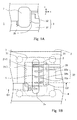
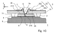
- FIG. 1A, FIG. 1B and FIG. 1C are views for explaining the configurations of an electric power semiconductor device according to Embodiment 1 of the present invention
- FIG. 1A is a partial plan view of the electric power semiconductor device
- FIG. 1B is a plan view illustrating the same portion as FIG. 1A when looked through a sealing resin and the base material portion of an interposer substrate
- FIG. 1C is a cross-sectional view including different cross-sectional positions taken by the line C1—C2 (parallel lines) in FIG. 1B when the sealing resin portion is removed.
- the rear side electrode of an electric power semiconductor element is adhered to one side, of a heat spreader, that is opposite to the other side, of the heat spreader, on which a heat radiation material is mounted.
- the front side electrode, on the surface of the electric power semiconductor element, for making main power flow is electrically connected through wire bonding with the portions, of electrode strips formed on the interposer substrate, that overlap part of the front side electrode when viewed in a direction that is perpendicular to the plane of the front side electrode.
- an aluminum chassis which functions as a heat radiation material 9, is attached to the rear side of a copper heat spreader 4 (15 mm ⁇ 20 mm ⁇ 1 mm (thickness)) through an insulating layer 8; a rear side electrode 21E of an IGBT (Insulated Gate Bipolar Transistor) of 10 mm ⁇ 10 mm, which is an electric power semiconductor element 2, is adhered to the front side of the heat spreader 4 by use of solder 6 (Sn-Ag-Cu, melting point: 217 °C).
- IGBT Insulated Gate Bipolar Transistor
- an interposer substrate 3 is disposed through a potting resin 71 in such a way as to face, with a predetermined gap, the heat spreader 4.
- the electric power semiconductor element 2 is disposed in the gap between the heat spreader 4 and the interposer substrate 3 in such a way that the rear side thereof is adhered to the heat spreader 4 and the front side thereof faces the rear side of the interposer substrate 3.
- a copper electrode strip 32 is formed on an glass-epoxy substrate 31 formed by impregnating glass fibers with an epoxy resin; the interposer substrate 3 is provided in such a way that at least part of a main power electrode 21C and a control electrode 21G, which are electrodes at the front side of the electric power semiconductor element 2, are exposed from an opening portion 3a (width 2 mm ⁇ length 15 mm).
- At least a bonding electrode 32p (wire bonding pad) to be connected with the main power electrode 21C (for example, a collector electrode) at the front side of the electric power semiconductor element 2 is disposed at a position where the bonding electrode 32p overlaps at least part of the main power electrode 21C when viewed in a direction (z) that is perpendicular to the plane of the interposer substrate 3.
- the portions exposed from the opening portion 3a of the main power electrode 21C include a bonding position for connecting the main power electrode 21C with the bonding electrode 32p and a space required for bonding.
- the main power electrode 21C on the front side of the electric power semiconductor element 2 and the bonding electrode 32p can be connected with each other through wire bonding utilizing an aluminum bonding wire 5 having a thickness of 0.5 mm from a position above the interposer substrate.
- the stroke length, in the extending direction of the plane (xy), of the bonding wire 5 is shorter than the distance (5 mm) between the center and the end of the main power electrode 21C.
- a bonding electrode 32p to be connected with the control electrode 21G (for example, a gate electrode) is also disposed at a position where the bonding electrode 32p overlaps at least part of the main power electrode 21C when viewed in the direction that is perpendicular to the plane of the interposer substrate 3.
- control electrode 21G is electrically connected with the gate-electrode bonding electrode 32p by use of a short-stroke-length bonding wire 5.
- the opening portion 3a has an opening that is longer than the y-direction length of the electric power semiconductor element 2.
- a predetermined position, of the heat spreader 4, that is exposed from the opening portion 3a is electrically connected with another bonding electrode 32p by use of the bonding wire 5.
- the space between the heat spreader 4 and the interposer substrate 3 and a predetermined region on the front side of the interposer substrate 3 is sealed with a sealing member 7 formed of a resin in such a way that the electric power semiconductor element 2 and the bonding wires 5 are wrapped.
- a sealing member 7 formed of a resin in such a way that the electric power semiconductor element 2 and the bonding wires 5 are wrapped.
- the bonding electrode 32p communicates with an external terminal portion 32e (the exposed portion thereof in FIG. 1A ) by way of a portion coated with a solder resist 35.
- the external terminal portion 32e exposed from the sealing member 7 electrically connects the respective electrodes 21 C, 21 G, and 21E formed on the electric power semiconductor element 2 with the outside.
- the opening portion 3a provided in the interposer substrate 3 is disposed in the situation where the bonding electrode 32p to be connected with the main power electrode 21C on the front side of the electric power semiconductor element 2 overlaps at least part of the main power electrode 21 C.
- the electrode strip 32 can be formed in such a way as to occupy some part of the region of the electric power semiconductor element 2 in the plane-extending direction (xy); thus, the mounting area can be suppressed. Because it is not required that the insulating layer 8 for making the heat spreader 4 and the heat radiation material 9 adhere to each other has such a rigidity as that of a circuit board, the heat conductivity can readily be secured.
- the electric power semiconductor element 2 communicates with the heat radiation material 9 through materials having a high heat conductivity; therefore, the generated heat can efficiently be radiated from the heat radiation material 9.
- the opening portion 3a the positional relationship with the electric power semiconductor element 2 is adjusted, is provided so that no processing for soldering is implemented.
- the width (in a direction that is parallel to the wire bonding: in the x direction in FIG. 1 ) of the opening portion 3a is larger than the bonding length of the wire bonding; when the insertion space of the tool for wire bonding is taken into consideration, the width should be the same as or larger than 200 % of the wire diameter.
- a high-flexibility material is utilized for the sealing member 7 in order to prevent the bonding wire 5 from being deformed and to secure the high insulating performance.
- the potting resin 71 which functions as a spacer, is required in order to form a desired gap between the heat spreader 4 and the interposer substrate 3; the potting resin 71 demonstrates an effect of preventing the surface of the electric power semiconductor element 2 having a complex shape such as a trench structure from directly making contact with the interposer substrate 3.
- the interposer substrate 3 is often screwed to the heat radiation material 9 for the purpose of pressing the heat spreader 4 against the heat radiation material 9.
- the potting resin 71 which functions as a spacer, receives the stress and transfers it to the heat spreader 4, so that there is demonstrated an effect of preventing the high-flexibility sealing member from being deformed and transferring the stress to the electric power semiconductor element 2 and the bonding wire 5.
- Embodiments after and including Embodiment 1 are explained with the interposer substrate 3, as an example, that is a kind of printed wire board; however, the embodiments are not limited to the interposer substrate 3, but can be applied to various kinds of printed wire board including, for example, a mother substrate.
- the interposer substrate 3 can be utilized as a printed wire board.
- the electric power semiconductor device 1 according to Embodiment 1 is provided with a heat spreader 4, which is a heat transfer plate, to the side opposite to the mounting side of which the heat radiation material 9 is adhered through the insulating layer 8; a printed wire board (the interposer substrate 3) that is disposed in such a way as to face, with a predetermined gap, the mounting side of the heat transfer plate (heat spreader 4), on the (outer) side of which, opposite to the (inner) side facing the heat transfer plate (heat spreader 4), the electrode strip 32 is formed, and in the vicinity of the electrode strip 32 of which, the opening portion 3a is provided; the electric power semiconductor element 2 that is disposed between the heat transfer plate (heat spreader 4) and the printed wire board (interposer substrate 3) and whose rear side is adhered to the mounting side of the heat transfer plate (heat spreader 4); and the bonding wire 5, which is a wiring member, one end of which is bonded to a first bonding portion of, for example,
- At least part of the second bonding portion (bonding electrode 32p) is included in a space that extends from the element electrode (main power electrode 21C) to the printed wire board (interposer substrate 3) in the direction (z) vertical to the mounting side, and the electrode strip 32 and the opening portion 3a are arranged in such a way that the first bonding portion is included in a space that extends from the opening portion 3a to the element electrode (main power electrode 21C) in the vertical (z) direction.
- the heat radiation performance can be secured; on top of that, even when without utilizing an electric power semiconductor element whose surface electrode is adjusted for soldering, wiring is implemented through ultrasonic bonding that requires operation from the front side, it is made possible that the electrode strip 32 overlaps the region of the front side electrode so that the mounting area is reduced.
- At least part of the electrode strip 32 on the printed wire board (interposer substrate 3) to be connected overlaps the front side electrode of the electric power semiconductor element 2 when viewed from the upper side (from a position apart from the electric power semiconductor element 2 in a direction vertical to the mounting side).
- downsizing of the slit (opening portion 3a) makes it possible to achieve downsizing of the mounting area and the occupation area of the printed wire board (interposer substrate 3).
- the wiring member is the bonding wire 5, which is a wire for bonding
- the opening portion 3a includes a region required for bonding the bonding wire 5 to the first bonding portion of the element electrode (main power electrode 21C).
- the electric power semiconductor element 2 is a vertical semiconductor element such as an IGBT, also on the rear side of which the electrode 21E is formed, and the bonding wire 5, which is a wiring member, electrically connects the heat transfer plate (heat spreader 4) to which the electrode 21E is adhered with another bonding portion (another bonding electrode 32p) of the electrode strip 32, through the opening portion 3a; therefore, it is made possible to readily obtain electric power semiconductor device 1 that is small-size and has superior heat radiation performance.
- Embodiment 2 the supporting structure for the interposer substrate is changed, in comparison with Embodiment 1, and the electric connection path is also changed by utilizing the supporting structure.
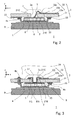
- FIG. 2 is a partial cross-sectional view for explaining the configuration of an electric power semiconductor device according to Embodiment 2 and corresponds to FIG. 1C in Embodiment 1; however, the cutting position corresponds to the portion where the line C2 in FIG. 1B is extended.
- FIG. 2 the constituent elements that are the same as those explained in Embodiment 1 are designated by the same characters and the explanation therefor will be omitted.
- the both ends of the heat spreader 4 are made to rise from the mounting side so that a tray shape is formed; then, a supporting portion 4s formed at each of the both ends supports the interposer substrate 3.
- a rear side electrode strip 33 is formed at a position corresponding to the position of the supporting portion 4s; by soldering the rear side electrode strip 33 with the supporting portion 4s, the position, with respect to the heat spreader 4, of the interposer substrate 3 is fixed. Accordingly, the potting resin 71 explained in Embodiment 1 is not utilized.
- part of the rear side electrode strip 33 of the interposer substrate 3 extends to the outside of the sealing member 7 and can be electrically connected with the outside at that portion.
- connection with the rear side electrode 21E of the electric power semiconductor element 2 does not require the wire bonding through the opening portion 3a described in Embodiment 1, the length of the opening portion 3a can be made shorter than the length of the main power electrode 21C on the front side. Accordingly, the restriction on the arrangement of the front side electrode strip 32 is reduced; thus, the mounting area can further be reduced.
- the supporting portion 4s that rises from the mounting side to the printed wire board (interposer substrate 3) and supports the printed wire board (interposer substrate 3) is formed at each of the both ends, of the heat transfer plate (heat spreader 4), that face each other.
- the electric power semiconductor element 2 is a vertical semiconductor element such as an IGBT, also on the rear side of which the electrode 21E is formed, and the electrode portion (rear side electrode strip 33) formed on the printed wire board (interposer substrate 3) and the supporting portion 4s are electrically connected with each other; therefore, for example, the length of the opening portion 3a can be made shorter than the size of the element and hence the mounting area can further be reduced.
- the electric connection member between the front side electrode of the electric power semiconductor element and the interposer substrate is changed in Embodiment 3. Moreover, in comparison with Embodiment 2, the structure of the portion where the interposer substrate and the heat spreader are electrically connected is changed.
- FIG. 3 is a partial cross-sectional view for explaining the configuration of an electric power semiconductor device according to Embodiment 3 and corresponds to the partial cross-sectional view in Embodiment 2.
- the constituent elements that are the same as those explained in Embodiment 2 are designated by the same characters and the explanation therefor will be omitted.
- Embodiment 3 not a bonding wire but an electrode member 51 is utilized for connecting the main power electrode 21C on the front side of the electric power semiconductor element 2 with a bonding electrode 32j (corresponding to the bonding electrode 32p explained in each of Embodiments 1 and 2) of the interposer substrate 3.
- the electrode member 51 is made of copper and has the shape of a so-called boater, i.e., a flat bottom portion 51t is formed on one end of a cylindrical body and a flange-shaped terminal portion 51j that extends toward the outer edge thereof is formed at the other end of the cylindrical body.
- the bottom portion 51t is inserted through the opening portion 3a, and ultrasonic bonding is applied to bond the main power electrode 21C with the bottom portion 51t; then, the terminal portion 51j is soldered with the bonding electrode 32j.
- an electric connection path from the main power electrode 21C on the front side of the electric power semiconductor element 2 to the outside is formed.
- the cross-sectional area of the electric connection path can readily be increased; thus, it is made possible to perform small-electric-resistance and high-reliability electric connection.
- one of the both ends of the heat spreader 4 is formed so as to be the supporting portion 4s as is the case with Embodiment 2; however, after being extended in the plane-extending direction (xy), as is the case with the supporting portion 4s, the other one thereof is formed so as to be a protrusion 4p that protrudes in the vertical direction (z).
- a through-hole coated with copper is formed at a position, in the interposer substrate 3, that corresponds to the protrusion 4p; the protrusion 4p that penetrates the through-hole is soldered with an electrode 34 in the through-hole.
- the position, with respect to the heat spreader 4, of the interposer substrate 3 is fixed, and an electric connection path to the rear side electrode 21E is formed on the front side of the interposer substrate 3.
- the opening portion 3a is downsized, so that the restriction on the arrangement of the front side electrode strip 32 is reduced; thus, the mounting area can further be decreased.
- the electrode member 51 in which the bottom portion 51t, which is a flat portion to be ultrasonic-bonded with the first bonding portion, and the terminal portion 51 j to be soldered with the bonding electrode 32j, which is the second bonding portion, are provided.
- At least one of the supporting portions 4s formed at both ends, of the heat transfer plate (heat spreader 4), that face each other is provided with the protrusion 4p that penetrates the through-hole provided in the printed wire board (interposer substrate 3) and is exposed at the second side (the outside).
- the electric power semiconductor element 2 is a vertical semiconductor element such as an IGBT, also on the rear side of which the electrode 21E is formed, and the electrode 34 in the through-hole, which is the electrode portion of the printed wire board (interposer substrate 3) and the protrusion 4p of the supporting portion 4s are electrically connected with each other.
- the wiring can be performed by utilizing only one side (outer side) of the printed wire board (interposer substrate 3); thus, the wiring can efficiently be performed.
- the heat spreader is divided into a plurality of independent plates by an insulator in Embodiment 4; respective electric power semiconductor elements mounted on the independent plates are connected directly through wire bonding without utilizing wiring leads on the interposer substrate.
- FIG. 4 is a partial cross-sectional view for explaining the configuration of an electric power semiconductor device according to Embodiment 4 and corresponds to the partial cross-sectional view in Embodiment 2.
- FIG. 4 the constituent elements that are the same as those explained in Embodiments 1 through 3 are designated by the same characters and the explanation therefor will be omitted.
- an insulating portion 4i formed of an insulating resin divides the heat spreader 4 into independent plates 4a and 4b and unillustrated depth-direction independent plates.
- a rear side electrode 21Ea of an electric power semiconductor element 2a and the independent plate 4a are soldered with the solder 6; a rear side electrode 21Eb of an electric power semiconductor element 2b and the independent plate 4b are soldered with the solder 6.
- the supporting portion 4s that protrudes toward the interposer substrate 3 but does not reach the interposer substrate 3.
- potting resin 71 which functions as a spacer, potting resins 71s and 71r are formed between the interposer substrate 3 and the heat spreader 4; as is the case with Embodiment 1, the potting resin 71r is formed in such a way as to be interposed between the independent plate 4b and the interposer substrate 3.
- one end of the potting resin 71s abuts on the interposer substrate 3; however, the other end thereof is formed in such a way as to be penetrated by the supporting portion 4s.
- the interposer substrate 3 is provided in such a way that at least part of a main power electrode 21Ca, which is the front side electrode of the electric power semiconductor element 2a adhered to the independent plate 4a, and an unillustrated control electrode 21Ga are exposed from the opening portion 3a formed therein.
- At least a bonding electrode 32p to be connected with the main power electrode 21 Ca at the front side of the electric power semiconductor element 2a is disposed at a position where the bonding electrode 32p overlaps at least part of the main power electrode 21Ca when viewed in a direction (z) that is perpendicular to the plane of the interposer substrate 3.
- the main power electrode 21 Ca on the front side of the electric power semiconductor element 2a and the bonding electrode 32p are electrically connected with each other through wire bonding utilizing an aluminum bonding wire 5a having a thickness of 0.5 mm from a position above the interposer substrate 3.
- the bonding electrode 32p to be connected with the control electrode 21Ga is also disposed at a position where the bonding electrode 32p overlaps at least part of the main power electrode 21Ca when viewed in the direction that is perpendicular to the plane of the interposer substrate 3.
- control electrode 21 Ga is electrically connected with the gate-electrode bonding electrode 32p by use of a short-stroke-length bonding wire.
- the protrusion 4p electrically connects the front side electrode 34 of the interposer substrate 3 with the independent plate 4b to which the rear side electrode 21Eb of the electric power semiconductor element 2b is adhered.
- the electric power semiconductor elements 2a and 2b are connected in series with each other; one end thereof can be connected with the electrode strip 32 through the opening portion 3a, and the other end thereof can be connected with the electrode 34 by way of the protrusion 4p.
- An unillustrated gate electrode 21 Gb of the electric power semiconductor element 2b is electrically connected with an unillustrated independent plate 4c (situated at a position behind the independent plate 4b in the drawing) by use of the bonding wire 5; furthermore, the gate electrode 21Gb can be connected with the front side of the interposer substrate 3 by way of another unillustrated protrusion insulated from the protrusion 4p in the drawing.
- the heat spreader 4 is preliminarily divided into a plurality of independent plates, and then an opening portion is provided for the electric power semiconductor element situated at a position that is one electrical end.
- the respective opening portions are provided for the both electric power semiconductor elements; however, it may also be allowed that as is the case with Embodiment 4, the protrusion 4p is utilized for the electric power semiconductor element situated at the other end.
- the protrusions can be utilized as external electrodes for electric connection.
- Coating the supporting portion 4s of the heat spreader 4 with an insulating resin (potting resin 71s) makes it possible to reinforce the supporting portion 4s while electrically insulating the supporting portion 4s.
- independent plates 4a, 4b, and so forth which are insulated from one another, are mechanically coupled by the insulating portions 4i, electric connection (wire bonding) between the electric power semiconductor elements (one electric power semiconductor element and its neighboring independent plate) can be implemented on a single heat spreader 4.
- the heat transfer plate (heat spreader 4) is configured with a plurality of electrically insulated independent plates 4a, 4b, and so forth; on the plurality of independent plates 4a, 4b, and so forth, a plurality of electric power semiconductor elements (2a, 2b) including the electric power semiconductor element 2a to which a wiring member (bonding wire 5a) is bonded, are separately mounted.
- the electric power semiconductor elements mounted on different independent plates are electrically connected with each other by use of another wiring member (bonding wire 5b) disposed between the heat transfer plate (heat spreader 4) and the printed wire board (interposer substrate 3).
- bonding wire 5b another wiring member disposed between the heat transfer plate (heat spreader 4) and the printed wire board (interposer substrate 3).
- the potting resin 71 can reduce the stress of screwing the board exerted on the soldering portion of the protrusion 4p. Accordingly, also in the electric power semiconductor device 1 according to any one of Embodiments 2 and 3, forming the potting resin 71, which is an insulator that functions as a spacer, as in Embodiment 1, makes it possible to reduce the stress of screwing the board exerted on the soldering portions of the supporting portion 4s and the protrusion 4p.
- the resin forming the sealing member 7 can be replaced by a silicone gel, or the sealing member 7 may be omitted when no weather problem is posed.
- the position of the opening portion 3a is specified at least for the main power electrode among the front side electrodes. This is because in the case where the control electrode (21G) and the main power electrode (21C) are formed on the same side, the main power electrode (collector electrode 21C) occupies most part of the side and hence the method of making the electrode occupying the side and the opening portion 3a overlap each other raises the effect of reducing the mounting area.
- the opening portion 3a is made to overlap an electrode occupying small area, some effect is demonstrated; therefore, it is not necessarily required to make the opening portion 3a overlap the main power electrode.
- the electric power semiconductor element 2 which is a main heat source in the electric power semiconductor device 1, is not limited to an IGBT, but may be another switching device such as a MOSFET (Metal Oxide Semiconductor Field Effect Transistor) or a device that as a rectifying device, controls electric power.
- MOSFET Metal Oxide Semiconductor Field Effect Transistor
- a so-called wide bandgap semiconductor whose base material is silicon carbide (SiC) is an example of suitable semiconductor material for remarkably demonstrating the effect of an electric power semiconductor device according to the present invention.
- a gallium nitride-based material, a diamond, or the like is utilized in addition to silicon carbide.
- the electric power semiconductor element 2 that functions as a switching device or a rectifying device, a wide bandgap semiconductor element is utilized, the power loss thereof is smaller than that of a conventional element formed of silicon; thus, the efficiency of the electric power semiconductor device can be raised. Because the withstanding voltage and the allowable current density thereof are high, the electric power semiconductor device can be downsized.
- a wide bandgap semiconductor element can be operated at a high temperature and hence it is made possible to downsize the heat radiation material 9 and to replace water cooling by air cooling; thus, the electric power semiconductor device can further be downsized.
- an SiC element is characterized by being capable of withstanding a higher temperature than an Si element is; therefore, the use-temperature environment of an electric power semiconductor device in which the foregoing electric power semiconductor element 2 is mounted may reach a temperature region where the temperature is higher than a conventional temperature.
Landscapes
- Engineering & Computer Science (AREA)
- Microelectronics & Electronic Packaging (AREA)
- Cooling Or The Like Of Semiconductors Or Solid State Devices (AREA)
- Chemical & Material Sciences (AREA)
- Materials Engineering (AREA)
- Ceramic Engineering (AREA)
Abstract
Description
- The present invention relates to a semiconductor device and particularly to an electric power semiconductor device that needs heat radiation performance.
- Electric power semiconductor devices have been widely spreading in all products such as industrial apparatuses, consumer electrical appliances, and information terminals; in particular, downsizing and high-reliability are required in consumer electrical appliances. Moreover, because an electric power semiconductor device deals with a high voltage and a large current, a great deal of heat is generated; thus, it is required to efficiently radiate the heat to the outside.
- Furthermore, it is also required that a wide bandgap semiconductor material such as SiC, which may be mainly utilized in the years to come because of a high operating temperature and a high efficiency thereof, can be applied to an electric power semiconductor device.
- In general, in a small electric power semiconductor device, an electric power semiconductor element is often disposed on a substrate on which an electric circuit is formed; when heat generated in the electric power semiconductor element is radiated to the outside through the substrate, the heat conductivity of the substrate itself provides a large effect to the heat radiation performance.
- However, an AlN substrate, which allegedly has superior heat conductivity, is difficult to obtain. In contrast, an alumina substrate or a glass-epoxy substrate, which is easily obtained, has heat conductivity of only one-twentieth to one-thousandth of the heat conductivity of high-heat-conductivity metal such as copper; therefore, high heat radiation performance cannot be expected.
- Accordingly, it is conceivable that in order to secure the heat radiation performance, the rear side of an electric power semiconductor element is directly connected with a heat radiation material through a high-heat-conductivity insulating layer. In that case, it is conceivable that wiring of the front side thereof is implemented by soldering the front side with an interposer substrate (e.g., refer to Patent Document 1).
- However, the electrode on the surface of a common electric power semiconductor element formed under the assumption of wire bonding is not suitable for soldering; therefore, soldering requires special machining. Thus, it is conceivable that an electric power semiconductor element is inserted into the opening of an interposer substrate and a technology (e.g., refer to
Patent Document 2 or 3) in which wiring of a common electric power semiconductor element can be implemented through wire bonding is utilized. -
-
Patent Document 1 - Japanese Patent Application Laid-Open
JP H10-012 812 A FIGS. 4 and 5) -
Patent Document 2 - Japanese Patent Application Laid-Open
JP H7-007 033 A FIGS. 1 and2 ) -
Patent Document 3 - Japanese Patent Application Laid-Open
JP 2004—014 0522 A FIG. 3 ) - However, such a structure as described above requires that a gap is provided in the plane-extending direction between the electric power semiconductor element and the interposer substrate; therefore, there has been a problem that in comparison with normal bare chip mounting in which an electric power semiconductor element and an electrode strip are arranged on a substrate, the mounting area is enlarged.
- The present invention has been implemented in order to solve the foregoing problems; the object thereof is to readily obtain a small-size electric power semiconductor device that has superior heat radiation performance.
- An electric power semiconductor device according to the present invention is provided with a heat transfer plate, to the side opposite to the mounting side of which a heat radiation material is adhered through an insulating layer, a printed wire board that is disposed in such a way as to face, with a predetermined gap, the mounting side of the heat transfer plate, on the side of which, opposite to the side facing the heat transfer plate, an electrode strip is formed, and in the vicinity of the electrode strip of which, an opening portion is provided, an electric power semiconductor element that is disposed between the heat transfer plate and the printed wire board and whose rear side is adhered to the mounting side of the heat transfer plate, and a wiring member, one end of which is bonded to a first bonding portion of an element electrode formed on the front side of the electric power semiconductor element and the other end of which is bonded to a second bonding portion of the electrode strip.
- The electric power semiconductor device is characterized in that the electrode strip and the opening portion are arranged in such a way that at least part of the second bonding portion is included in a space that extends from the element electrode to the printed wire board in a direction vertical to the mounting side and in such a way that the first bonding portion is included in a space that extends from the opening portion to the element electrode in the vertical direction.
- Because the present invention makes it possible to make the electrode strip of the printed wire board approach the electrode-surface region of the electric power semiconductor element, it is made possible to readily obtain a small-size electric power semiconductor device that has superior heat radiation performance.
-
- FIG. 1A, FIG. 1B and FIG. 1C
- are views for explaining the configuration of an electric power semiconductor device according to
Embodiment 1 of the present invention, including a partial plan view of the electric power semiconductor device, a partial plan view when looked through some materials, and a partial cross-sectional view; - FIG. 2
- is a partial cross-sectional view for explaining the configuration of an electric power semiconductor device according to
Embodiment 2 of the present invention; - FIG. 3
- is a partial cross-sectional view for explaining the configuration of an electric power semiconductor device according to
Embodiment 3 of the present invention; and - FIG. 4
- is a partial cross-sectional view for explaining the configuration of an electric power semiconductor device according to
Embodiment 4 of the present invention. -
FIG. 1A, FIG. 1B andFIG. 1C are views for explaining the configurations of an electric power semiconductor device according toEmbodiment 1 of the present invention;FIG. 1A is a partial plan view of the electric power semiconductor device;FIG. 1B is a plan view illustrating the same portion asFIG. 1A when looked through a sealing resin and the base material portion of an interposer substrate;FIG. 1C is a cross-sectional view including different cross-sectional positions taken by the line C1—C2 (parallel lines) inFIG. 1B when the sealing resin portion is removed. - In an electric
power semiconductor device 1 according toEmbodiment 1, the rear side electrode of an electric power semiconductor element is adhered to one side, of a heat spreader, that is opposite to the other side, of the heat spreader, on which a heat radiation material is mounted. - Furthermore, the front side electrode, on the surface of the electric power semiconductor element, for making main power flow is electrically connected through wire bonding with the portions, of electrode strips formed on the interposer substrate, that overlap part of the front side electrode when viewed in a direction that is perpendicular to the plane of the front side electrode. The details will be explained below.
- As illustrated in
FIGS. 1B and1C , an aluminum chassis, which functions as aheat radiation material 9, is attached to the rear side of a copper heat spreader 4 (15 mm × 20 mm × 1 mm (thickness)) through aninsulating layer 8; arear side electrode 21E of an IGBT (Insulated Gate Bipolar Transistor) of 10 mm × 10 mm, which is an electricpower semiconductor element 2, is adhered to the front side of theheat spreader 4 by use of solder 6 (Sn-Ag-Cu, melting point: 217 °C). - At the front side, of the
heat spreader 4, to which the electricpower semiconductor element 2 is adhered, aninterposer substrate 3 is disposed through apotting resin 71 in such a way as to face, with a predetermined gap, theheat spreader 4. - In other words, the electric
power semiconductor element 2 is disposed in the gap between theheat spreader 4 and theinterposer substrate 3 in such a way that the rear side thereof is adhered to theheat spreader 4 and the front side thereof faces the rear side of theinterposer substrate 3. - In the
interposer substrate 3, acopper electrode strip 32 is formed on an glass-epoxy substrate 31 formed by impregnating glass fibers with an epoxy resin; theinterposer substrate 3 is provided in such a way that at least part of amain power electrode 21C and acontrol electrode 21G, which are electrodes at the front side of the electricpower semiconductor element 2, are exposed from anopening portion 3a (width 2 mm × length 15 mm). - Out of the
electrode strip 32, at least abonding electrode 32p (wire bonding pad) to be connected with themain power electrode 21C (for example, a collector electrode) at the front side of the electricpower semiconductor element 2 is disposed at a position where thebonding electrode 32p overlaps at least part of themain power electrode 21C when viewed in a direction (z) that is perpendicular to the plane of theinterposer substrate 3. - The portions exposed from the
opening portion 3a of themain power electrode 21C include a bonding position for connecting themain power electrode 21C with thebonding electrode 32p and a space required for bonding. - Accordingly, the
main power electrode 21C on the front side of the electricpower semiconductor element 2 and thebonding electrode 32p can be connected with each other through wire bonding utilizing analuminum bonding wire 5 having a thickness of 0.5 mm from a position above the interposer substrate. - In this situation, the stroke length, in the extending direction of the plane (xy), of the
bonding wire 5 is shorter than the distance (5 mm) between the center and the end of themain power electrode 21C. - In
Embodiment 1, abonding electrode 32p to be connected with thecontrol electrode 21G (for example, a gate electrode) is also disposed at a position where thebonding electrode 32p overlaps at least part of themain power electrode 21C when viewed in the direction that is perpendicular to the plane of theinterposer substrate 3. - As is the case with the
main power electrode 21C, thecontrol electrode 21G is electrically connected with the gate-electrode bonding electrode 32p by use of a short-stroke-length bonding wire 5. - The
opening portion 3a has an opening that is longer than the y-direction length of the electricpower semiconductor element 2. A predetermined position, of theheat spreader 4, that is exposed from theopening portion 3a is electrically connected with anotherbonding electrode 32p by use of thebonding wire 5. - The space between the
heat spreader 4 and theinterposer substrate 3 and a predetermined region on the front side of theinterposer substrate 3 is sealed with a sealingmember 7 formed of a resin in such a way that the electricpower semiconductor element 2 and thebonding wires 5 are wrapped. As a result, the electricpower semiconductor device 1 having such an appearance (partial appearance) as illustrated inFIG. 1A is formed. - In the
electrode strip 32, thebonding electrode 32p communicates with anexternal terminal portion 32e (the exposed portion thereof inFIG. 1A ) by way of a portion coated with a solder resist 35. As a result, the externalterminal portion 32e exposed from the sealingmember 7 electrically connects therespective electrodes power semiconductor element 2 with the outside. - In the electric
power semiconductor device 1 configured as described above, theopening portion 3a provided in theinterposer substrate 3 is disposed in the situation where thebonding electrode 32p to be connected with themain power electrode 21C on the front side of the electricpower semiconductor element 2 overlaps at least part of themain power electrode 21 C. - Accordingly, the
electrode strip 32 can be formed in such a way as to occupy some part of the region of the electricpower semiconductor element 2 in the plane-extending direction (xy); thus, the mounting area can be suppressed. Because it is not required that the insulatinglayer 8 for making theheat spreader 4 and theheat radiation material 9 adhere to each other has such a rigidity as that of a circuit board, the heat conductivity can readily be secured. - When the electric
power semiconductor device 1 configured as described above is made to operate, a current flows in the electricpower semiconductor element 2 and hence the electricpower semiconductor element 2 develops heat. The heat generated in the electricpower semiconductor element 2 is transferred to theheat radiation material 9 through theheat spreader 4. - In this situation, the electric
power semiconductor element 2 communicates with theheat radiation material 9 through materials having a high heat conductivity; therefore, the generated heat can efficiently be radiated from theheat radiation material 9. In other words, theopening portion 3a, the positional relationship with the electricpower semiconductor element 2 is adjusted, is provided so that no processing for soldering is implemented. - Therefore, even when there is utilized an electric power semiconductor element for which it is required to implement wiring that needs operation in a predetermined direction as is the case with ultrasonic wire bonding, a compact, high-radiation-performance, and high-reliability electric power semiconductor device can be obtained.
- It is required that the width (in a direction that is parallel to the wire bonding: in the x direction in
FIG. 1 ) of theopening portion 3a is larger than the bonding length of the wire bonding; when the insertion space of the tool for wire bonding is taken into consideration, the width should be the same as or larger than 200 % of the wire diameter. - In many cases, a high-flexibility material is utilized for the sealing
member 7 in order to prevent thebonding wire 5 from being deformed and to secure the high insulating performance. The pottingresin 71, which functions as a spacer, is required in order to form a desired gap between theheat spreader 4 and theinterposer substrate 3; thepotting resin 71 demonstrates an effect of preventing the surface of the electricpower semiconductor element 2 having a complex shape such as a trench structure from directly making contact with theinterposer substrate 3. - In order to secure the heat radiation performance, the
interposer substrate 3 is often screwed to theheat radiation material 9 for the purpose of pressing theheat spreader 4 against theheat radiation material 9. The pottingresin 71, which functions as a spacer, receives the stress and transfers it to theheat spreader 4, so that there is demonstrated an effect of preventing the high-flexibility sealing member from being deformed and transferring the stress to the electricpower semiconductor element 2 and thebonding wire 5. - Accordingly, the harder is the potting resin 71 (the higher is the elastic modulus thereof) in comparison with the sealing
member 7, the larger effect can be demonstrated. - Embodiments after and including
Embodiment 1 are explained with theinterposer substrate 3, as an example, that is a kind of printed wire board; however, the embodiments are not limited to theinterposer substrate 3, but can be applied to various kinds of printed wire board including, for example, a mother substrate. - In other words, in an electric power semiconductor device according to each of the embodiments after and including
Embodiment 1, theinterposer substrate 3 can be utilized as a printed wire board. - As described above, the electric power semiconductor device 1 according to Embodiment 1 is provided with a heat spreader 4, which is a heat transfer plate, to the side opposite to the mounting side of which the heat radiation material 9 is adhered through the insulating layer 8; a printed wire board (the interposer substrate 3) that is disposed in such a way as to face, with a predetermined gap, the mounting side of the heat transfer plate (heat spreader 4), on the (outer) side of which, opposite to the (inner) side facing the heat transfer plate (heat spreader 4), the electrode strip 32 is formed, and in the vicinity of the electrode strip 32 of which, the opening portion 3a is provided; the electric power semiconductor element 2 that is disposed between the heat transfer plate (heat spreader 4) and the printed wire board (interposer substrate 3) and whose rear side is adhered to the mounting side of the heat transfer plate (heat spreader 4); and the bonding wire 5, which is a wiring member, one end of which is bonded to a first bonding portion of, for example, the main power electrode 21C which is an element electrode formed on the front side of the electric power semiconductor element 2 and the other end of which is bonded to the bonding electrode 32p which is a second bonding portion of the electrode strip 32.
- At least part of the second bonding portion (
bonding electrode 32p) is included in a space that extends from the element electrode (main power electrode 21C) to the printed wire board (interposer substrate 3) in the direction (z) vertical to the mounting side, and theelectrode strip 32 and theopening portion 3a are arranged in such a way that the first bonding portion is included in a space that extends from theopening portion 3a to the element electrode (main power electrode 21C) in the vertical (z) direction. - As a result, the heat radiation performance can be secured; on top of that, even when without utilizing an electric power semiconductor element whose surface electrode is adjusted for soldering, wiring is implemented through ultrasonic bonding that requires operation from the front side, it is made possible that the
electrode strip 32 overlaps the region of the front side electrode so that the mounting area is reduced. - In other words, it is made possible to readily obtain a small-size electric power semiconductor device that has superior heat radiation performance.
- Almost all of the front side of the electric
power semiconductor element 2 is configured with wire bonding electrodes, and in order to expose all of the electrodes, it is required to form a slit (corresponding to theopening portion 3a in Embodiment 1) larger than the electricpower semiconductor element 2; therefore, there has been a problem that the mounting area is enlarged in comparison with a normal bare chip mounting. - However, in the electric
power semiconductor device 1 according toEmbodiment 1, at least part of theelectrode strip 32 on the printed wire board (interposer substrate 3) to be connected overlaps the front side electrode of the electricpower semiconductor element 2 when viewed from the upper side (from a position apart from the electricpower semiconductor element 2 in a direction vertical to the mounting side). - Accordingly, downsizing of the slit (opening
portion 3a) makes it possible to achieve downsizing of the mounting area and the occupation area of the printed wire board (interposer substrate 3). - In particular, the wiring member is the
bonding wire 5, which is a wire for bonding, and theopening portion 3a includes a region required for bonding thebonding wire 5 to the first bonding portion of the element electrode (main power electrode 21C). - Therefore, it is made possible to implement bonding through the
opening portion 3a and hence an electric power semiconductor device can efficiently be produced. Moreover, because the stroke length of the bonding is reduced, the electric resistance can also be decreased. - The electric
power semiconductor element 2 is a vertical semiconductor element such as an IGBT, also on the rear side of which theelectrode 21E is formed, and thebonding wire 5, which is a wiring member, electrically connects the heat transfer plate (heat spreader 4) to which theelectrode 21E is adhered with another bonding portion (anotherbonding electrode 32p) of theelectrode strip 32, through theopening portion 3a; therefore, it is made possible to readily obtain electricpower semiconductor device 1 that is small-size and has superior heat radiation performance. - In
Embodiment 2, the supporting structure for the interposer substrate is changed, in comparison withEmbodiment 1, and the electric connection path is also changed by utilizing the supporting structure. -
FIG. 2 is a partial cross-sectional view for explaining the configuration of an electric power semiconductor device according toEmbodiment 2 and corresponds toFIG. 1C inEmbodiment 1; however, the cutting position corresponds to the portion where the line C2 inFIG. 1B is extended. - In
FIG. 2 , the constituent elements that are the same as those explained inEmbodiment 1 are designated by the same characters and the explanation therefor will be omitted. - As illustrated in
FIG. 2 , inEmbodiment 2, the both ends of theheat spreader 4 are made to rise from the mounting side so that a tray shape is formed; then, a supportingportion 4s formed at each of the both ends supports theinterposer substrate 3. - On the rear side of the
interposer substrate 3, a rearside electrode strip 33 is formed at a position corresponding to the position of the supportingportion 4s; by soldering the rearside electrode strip 33 with the supportingportion 4s, the position, with respect to theheat spreader 4, of theinterposer substrate 3 is fixed. Accordingly, the pottingresin 71 explained inEmbodiment 1 is not utilized. - Furthermore, part of the rear
side electrode strip 33 of theinterposer substrate 3 extends to the outside of the sealingmember 7 and can be electrically connected with the outside at that portion. As a result, because connection with therear side electrode 21E of the electricpower semiconductor element 2 does not require the wire bonding through theopening portion 3a described inEmbodiment 1, the length of theopening portion 3a can be made shorter than the length of themain power electrode 21C on the front side. Accordingly, the restriction on the arrangement of the frontside electrode strip 32 is reduced; thus, the mounting area can further be reduced. - As described above, in the electric
power semiconductor device 1 according toEmbodiment 2 of the present invention, the supportingportion 4s that rises from the mounting side to the printed wire board (interposer substrate 3) and supports the printed wire board (interposer substrate 3) is formed at each of the both ends, of the heat transfer plate (heat spreader 4), that face each other. - Therefore, it is made possible that the gap between the printed wire board (interposer substrate 3) and the
heat spreader 4 is secured, that the productivity is raised, and that the airtightness of the sealingmember 7 is enhanced. - The electric
power semiconductor element 2 is a vertical semiconductor element such as an IGBT, also on the rear side of which theelectrode 21E is formed, and the electrode portion (rear side electrode strip 33) formed on the printed wire board (interposer substrate 3) and the supportingportion 4s are electrically connected with each other; therefore, for example, the length of theopening portion 3a can be made shorter than the size of the element and hence the mounting area can further be reduced. - In comparison with each of
Embodiments Embodiment 3. Moreover, in comparison withEmbodiment 2, the structure of the portion where the interposer substrate and the heat spreader are electrically connected is changed. -
FIG. 3 is a partial cross-sectional view for explaining the configuration of an electric power semiconductor device according toEmbodiment 3 and corresponds to the partial cross-sectional view inEmbodiment 2. InFIG. 3 , the constituent elements that are the same as those explained inEmbodiment 2 are designated by the same characters and the explanation therefor will be omitted. - As illustrated in
FIG. 3 , inEmbodiment 3, not a bonding wire but anelectrode member 51 is utilized for connecting themain power electrode 21C on the front side of the electricpower semiconductor element 2 with abonding electrode 32j (corresponding to thebonding electrode 32p explained in each ofEmbodiments 1 and 2) of theinterposer substrate 3. - The
electrode member 51 is made of copper and has the shape of a so-called boater, i.e., aflat bottom portion 51t is formed on one end of a cylindrical body and a flange-shapedterminal portion 51j that extends toward the outer edge thereof is formed at the other end of the cylindrical body. - The
bottom portion 51t is inserted through theopening portion 3a, and ultrasonic bonding is applied to bond themain power electrode 21C with thebottom portion 51t; then, theterminal portion 51j is soldered with thebonding electrode 32j. - As a result, an electric connection path from the
main power electrode 21C on the front side of the electricpower semiconductor element 2 to the outside is formed. In this case, the cross-sectional area of the electric connection path can readily be increased; thus, it is made possible to perform small-electric-resistance and high-reliability electric connection. - Moreover, one of the both ends of the
heat spreader 4 is formed so as to be the supportingportion 4s as is the case withEmbodiment 2; however, after being extended in the plane-extending direction (xy), as is the case with the supportingportion 4s, the other one thereof is formed so as to be aprotrusion 4p that protrudes in the vertical direction (z). - A through-hole coated with copper is formed at a position, in the
interposer substrate 3, that corresponds to theprotrusion 4p; theprotrusion 4p that penetrates the through-hole is soldered with anelectrode 34 in the through-hole. - Accordingly, the position, with respect to the
heat spreader 4, of theinterposer substrate 3 is fixed, and an electric connection path to therear side electrode 21E is formed on the front side of theinterposer substrate 3. - As a result, it is made possible to fix the gap between the
interposer substrate 3 and theheat spreader 4 without utilizing the pottingresin 71 and to perform positioning in the plane-extending direction (xy). Additionally, as is the case withEmbodiment 2, theopening portion 3a is downsized, so that the restriction on the arrangement of the frontside electrode strip 32 is reduced; thus, the mounting area can further be decreased. - As described above, in the electric
power semiconductor device 1 according toEmbodiment 3, as the wiring member to be bonded with themain power electrode 21C, there is utilized theelectrode member 51 in which thebottom portion 51t, which is a flat portion to be ultrasonic-bonded with the first bonding portion, and theterminal portion 51 j to be soldered with thebonding electrode 32j, which is the second bonding portion, are provided. - Therefore, it is made possible to form a circuit whose electric resistance is smaller than that at a time when, for example, a solder bump and a through-hole are utilized.
- Moreover, at least one of the supporting
portions 4s formed at both ends, of the heat transfer plate (heat spreader 4), that face each other is provided with theprotrusion 4p that penetrates the through-hole provided in the printed wire board (interposer substrate 3) and is exposed at the second side (the outside). - Therefore, positioning of the printed wire board (interposer substrate 3) in the plane-extending direction (xy) can readily be implemented.
- Furthermore, the electric
power semiconductor element 2 is a vertical semiconductor element such as an IGBT, also on the rear side of which theelectrode 21E is formed, and theelectrode 34 in the through-hole, which is the electrode portion of the printed wire board (interposer substrate 3) and theprotrusion 4p of the supportingportion 4s are electrically connected with each other. - Therefore, the wiring can be performed by utilizing only one side (outer side) of the printed wire board (interposer substrate 3); thus, the wiring can efficiently be performed.
- In comparison with each of
Embodiments 1 through 3, the heat spreader is divided into a plurality of independent plates by an insulator inEmbodiment 4; respective electric power semiconductor elements mounted on the independent plates are connected directly through wire bonding without utilizing wiring leads on the interposer substrate. - Moreover, the protrusion of the heat spreader is divided into a plurality portions through insulation so that the respective portions can be utilized as external electrodes.
FIG. 4 is a partial cross-sectional view for explaining the configuration of an electric power semiconductor device according toEmbodiment 4 and corresponds to the partial cross-sectional view inEmbodiment 2. - In
FIG. 4 , the constituent elements that are the same as those explained inEmbodiments 1 through 3 are designated by the same characters and the explanation therefor will be omitted. - As illustrated in
FIG. 4 , an insulatingportion 4i formed of an insulating resin divides theheat spreader 4 intoindependent plates - A rear side electrode 21Ea of an electric
power semiconductor element 2a and theindependent plate 4a are soldered with thesolder 6; a rear side electrode 21Eb of an electricpower semiconductor element 2b and theindependent plate 4b are soldered with thesolder 6. - As is the case with
Embodiment 3, at one end (at the right side of the drawing) of theindependent plate 4b, there is formed theprotrusion 4p that penetrates a through-hole formed in theinterposer substrate 3 and is soldered with theelectrode 34 in the through-hole. - In contrast, at one end (at the left side of the drawing) of the
independent plate 4a, there is formed the supportingportion 4s that protrudes toward theinterposer substrate 3 but does not reach theinterposer substrate 3. - As the
potting resin 71 which functions as a spacer, potting resins 71s and 71r are formed between theinterposer substrate 3 and theheat spreader 4; as is the case withEmbodiment 1, thepotting resin 71r is formed in such a way as to be interposed between theindependent plate 4b and theinterposer substrate 3. - In contrast, one end of the
potting resin 71s abuts on theinterposer substrate 3; however, the other end thereof is formed in such a way as to be penetrated by the supportingportion 4s. - The
interposer substrate 3 is provided in such a way that at least part of a main power electrode 21Ca, which is the front side electrode of the electricpower semiconductor element 2a adhered to theindependent plate 4a, and an unillustrated control electrode 21Ga are exposed from theopening portion 3a formed therein. - Out of the
electrode strip 32, at least abonding electrode 32p to be connected with the main power electrode 21 Ca at the front side of the electricpower semiconductor element 2a is disposed at a position where thebonding electrode 32p overlaps at least part of the main power electrode 21Ca when viewed in a direction (z) that is perpendicular to the plane of theinterposer substrate 3. - The main power electrode 21 Ca on the front side of the electric
power semiconductor element 2a and thebonding electrode 32p are electrically connected with each other through wire bonding utilizing analuminum bonding wire 5a having a thickness of 0.5 mm from a position above theinterposer substrate 3. - Also in
Embodiment 4, thebonding electrode 32p to be connected with the control electrode 21Ga is also disposed at a position where thebonding electrode 32p overlaps at least part of the main power electrode 21Ca when viewed in the direction that is perpendicular to the plane of theinterposer substrate 3. - As is the case with the main power electrode 21 Ca, the control electrode 21 Ga is electrically connected with the gate-
electrode bonding electrode 32p by use of a short-stroke-length bonding wire. - In contrast, no opening portion is formed at a position, in the
interposer substrate 3, that is right above the electricpower semiconductor element 2b adhered to theindependent plate 4b; a main power electrode 21Cb of the electricpower semiconductor element 2b is electrically connected with theindependent plate 4a by use of abonding wire 5b. - The
protrusion 4p electrically connects thefront side electrode 34 of theinterposer substrate 3 with theindependent plate 4b to which the rear side electrode 21Eb of the electricpower semiconductor element 2b is adhered. - In other words, the electric
power semiconductor elements electrode strip 32 through theopening portion 3a, and the other end thereof can be connected with theelectrode 34 by way of theprotrusion 4p. - An unillustrated gate electrode 21 Gb of the electric
power semiconductor element 2b is electrically connected with an unillustrated independent plate 4c (situated at a position behind theindependent plate 4b in the drawing) by use of thebonding wire 5; furthermore, the gate electrode 21Gb can be connected with the front side of theinterposer substrate 3 by way of another unillustrated protrusion insulated from theprotrusion 4p in the drawing. - In many cases, when in an electric power semiconductor device, a plurality of electric power semiconductor elements are utilized, a plurality of electric power semiconductor devices are utilized in such a way as to be connected with one another.
- In this situation, when the electric power semiconductor elements are connected directly with one another, the number of wiring leads can be reduced, in comparison with the case where all the electrodes of the electric power semiconductor elements are connected with interposer substrates by use of bonding wires.
- In this situation, the
heat spreader 4 is preliminarily divided into a plurality of independent plates, and then an opening portion is provided for the electric power semiconductor element situated at a position that is one electrical end. - In that case, it may also possible that the respective opening portions are provided for the both electric power semiconductor elements; however, it may also be allowed that as is the case with
Embodiment 4, theprotrusion 4p is utilized for the electric power semiconductor element situated at the other end. - In that case, when the two or more protrusions are insulated from one another, the protrusions can be utilized as external electrodes for electric connection. Coating the supporting
portion 4s of theheat spreader 4 with an insulating resin (pottingresin 71s) makes it possible to reinforce the supportingportion 4s while electrically insulating the supportingportion 4s. - Furthermore, because the
independent plates portions 4i, electric connection (wire bonding) between the electric power semiconductor elements (one electric power semiconductor element and its neighboring independent plate) can be implemented on asingle heat spreader 4. - As described above, in the electric
power semiconductor device 1 according toEmbodiment 4, the heat transfer plate (heat spreader 4) is configured with a plurality of electrically insulatedindependent plates independent plates power semiconductor element 2a to which a wiring member (bonding wire 5a) is bonded, are separately mounted. - Among the plurality of electric power semiconductor elements, the electric power semiconductor elements mounted on different independent plates are electrically connected with each other by use of another wiring member (
bonding wire 5b) disposed between the heat transfer plate (heat spreader 4) and the printed wire board (interposer substrate 3). Thus, by utilizing the space, downsizing can further be achieved. - As described in
Embodiment 4, even when theprotrusion 4p is formed in theheat spreader 4, the pottingresin 71 can reduce the stress of screwing the board exerted on the soldering portion of theprotrusion 4p. Accordingly, also in the electricpower semiconductor device 1 according to any one ofEmbodiments resin 71, which is an insulator that functions as a spacer, as inEmbodiment 1, makes it possible to reduce the stress of screwing the board exerted on the soldering portions of the supportingportion 4s and theprotrusion 4p. - In each of forgoing Embodiments, even when instead of copper, aluminum, iron, or copper-tungsten is utilized as the material of the
heat spreader 4, the same effect can be demonstrated. In each of forgoing Embodiments, there has been described a case where as the material for the wire bonding, aluminum is utilized; however, use of copper or a metal wire can demonstrate the same effect. - There has been described a case where as the material for the soldering, Sn—Ag—Cu system is utilized; however, use of SnSb or SnBi can obtain the same effect. Furthermore, even when instead of solder, a conductive adhesive is utilized, the same effect can be obtained.
- It is also made possible to utilize heat conductive grease for the insulating
layer 8, instead of a so-called insulation sheet. The resin forming the sealingmember 7 can be replaced by a silicone gel, or the sealingmember 7 may be omitted when no weather problem is posed. - In each of foregoing Embodiments, as an example of material, of the interposer substrate, that can readily be obtained without considering the heat conductivity, a glass-epoxy substrate has been described; however, even when a paper phenol substrate, a polyimide substrate, an alumina substrate, or an aluminum-based metal substrate is utilized, the same effect can be obtained.
- In each of foregoing Embodiments, the position of the
opening portion 3a is specified at least for the main power electrode among the front side electrodes. This is because in the case where the control electrode (21G) and the main power electrode (21C) are formed on the same side, the main power electrode (collector electrode 21C) occupies most part of the side and hence the method of making the electrode occupying the side and theopening portion 3a overlap each other raises the effect of reducing the mounting area. - However, even when the
opening portion 3a is made to overlap an electrode occupying small area, some effect is demonstrated; therefore, it is not necessarily required to make theopening portion 3a overlap the main power electrode. - It goes without saying that the constituent elements in each of foregoing
Embodiments 1 through 3 can be increased or decreased in number or can be combined with one another in an appropriate manner. - Each of the drawings utilized in the foregoing explanation of the electric
power semiconductor device 1 is a schematic diagram in which only main members are illustrated; it goes without saying that in a practical electric power semiconductor device, various configurations are utilized. - In each of the drawings, the electric
power semiconductor element 2, which is a main heat source in the electricpower semiconductor device 1, is not limited to an IGBT, but may be another switching device such as a MOSFET (Metal Oxide Semiconductor Field Effect Transistor) or a device that as a rectifying device, controls electric power. - As an effect of the present invention, it has been described that even when a device whose front side electrode does not fit soldering is utilized, the heat radiation performance and downsizing can be secured; however, this does not suggest that a device that fits soldering, for example, a device having a front side electrode on which a copper or gold layer is formed, is excluded.
- A so-called wide bandgap semiconductor whose base material is silicon carbide (SiC) is an example of suitable semiconductor material for remarkably demonstrating the effect of an electric power semiconductor device according to the present invention. As the material of a wide bandgap semiconductor, a gallium nitride-based material, a diamond, or the like is utilized in addition to silicon carbide.
- For example, when as the electric
power semiconductor element 2 that functions as a switching device or a rectifying device, a wide bandgap semiconductor element is utilized, the power loss thereof is smaller than that of a conventional element formed of silicon; thus, the efficiency of the electric power semiconductor device can be raised. Because the withstanding voltage and the allowable current density thereof are high, the electric power semiconductor device can be downsized. - Moreover, because having a high heat resistance, a wide bandgap semiconductor element can be operated at a high temperature and hence it is made possible to downsize the
heat radiation material 9 and to replace water cooling by air cooling; thus, the electric power semiconductor device can further be downsized. - However, an SiC element is characterized by being capable of withstanding a higher temperature than an Si element is; therefore, the use-temperature environment of an electric power semiconductor device in which the foregoing electric
power semiconductor element 2 is mounted may reach a temperature region where the temperature is higher than a conventional temperature. - Accordingly, the importance of the heat radiation performance further increases, and hence the effect of the present invention, i.e., the high heat radiation performance and the capability of downsizing are more remarkably demonstrated.
- In other words, even when by taking advantage of the characteristics of a wide bandgap semiconductor, the downsizing and the efficiency hike are promoted, it is made possible to improve the heat-cycle resistance and the power-cycle resistance of an electric power semiconductor device and to achieve the lifetime prolongation of the electric power semiconductor device. That is to say, by exerting an effect of the present invention, the characteristics of a wide bandgap semiconductor can be utilized.
-
- 1
- electric power semiconductor device
- 2
- electric power semiconductor element
- 21C
- main power electrode (element electrode)
- 21E
- rear side electrode
- 3
- interposer substrate (printed wire board)
- 3a
- opening portion
- 31
- base material
- 32
- electrode strip
- 32p
- bonding electrode (2nd bonding portion)
- 32j
- bonding electrode (2nd bonding portion)
- 33
- rear side electrode strip (electrode portion)
- 34
- through-hole electrode (electrode portion)
- 35
- solder resist
- 4
- heat spreader (heat transfer plate)
- 4s
- supporting portion
- 4p
- protrusion
- 5
- bonding wire (wiring member)
- 8
- insulating layer
- 9
- heat radiation material
- 51
- electrode member (wiring member)
- 51t
- bottom portion (flat portion)
- 51j
- terminal portion
Claims (10)
- An electric power semiconductor device comprising:- a heat transfer plate, to the side opposite to the mounting side of which a heat radiation material is adhered through an insulating layer;- a printed wire board that is disposed in such a way as to face, with a predetermined gap, the mounting side of the heat transfer plate, on the side of which, opposite to the side facing the heat transfer plate, an electrode strip is formed, and in the vicinity of the electrode strip of which, an opening portion is provided;- an electric power semiconductor element that is disposed between the heat transfer plate and the printed wire board and whose rear side is adhered to the mounting side of the heat transfer plate; and- a wiring member, one end of which is bonded to a first bonding portion of an element electrode formed on the front side of the electric power semiconductor element and the other end of which is bonded to a second bonding portion of the electrode strip,- wherein the electrode strip and the opening portion are arranged in such a way that at least part of the second bonding portion is included in a space that extends from the element electrode to the printed wire board in a direction vertical to the mounting side and in such a way that the first bonding portion is included in a space that extends from the opening portion to the element electrode in the vertical direction.
- The electric power semiconductor device according to claim 1,
wherein the wiring member is a bonding wire, and the opening portion has a region necessary for bonding the bonding wire to the first bonding portion. - The electric power semiconductor device according to claim 1,
wherein the wiring member is an electrode member in which a flat portion to be ultrasonic-bonded to the first bonding portion and a terminal portion to be soldered with the second bonding portion are provided. - The electric power semiconductor device according to any one of claims 1 through 3,
wherein a supporting portion that rises from the mounting side to the printed wire board and supports the printed wire board is formed at each of both ends, of the heat transfer plate, that face each other. - The electric power semiconductor device according to claim 4,
wherein at least one of the supporting portions formed at both ends that face each other is provided with a protrusion that penetrates a through-hole provided in the printed wire board and is exposed at a second side. - The electric power semiconductor device according to any one of claims 1 through 5,
wherein the electric power semiconductor element is a vertical semiconductor element, also on the rear side of which an electrode is formed, and
wherein a wiring member electrically connects the heat transfer plate with another bonding portion of the electrode strip through the opening portion. - The electric power semiconductor device according to any one of claims 4 and 5,
wherein the electric power semiconductor element is a vertical semiconductor element, also on the rear side of which an electrode is formed, and
wherein an electrode portion formed on the printed wire board and the supporting portion are electrically connected with each other. - The electric power semiconductor device according to any one of claims 1 through 7,
wherein the heat transfer plate is formed of a plurality of independent plates that are insulated from one another,
wherein respective electric power semiconductor elements including electric power semiconductor elements, to each of which a wiring member is bonded, are mounted on the plurality of independent plates, and wherein among the plurality of electric power semiconductor elements, the electric power semiconductor elements mounted on different independent plates are electrically connected with each other by use of another wiring member disposed between the heat transfer plate and the printed wire board. - The electric power semiconductor device according to any one of claims 1 through 8,
wherein the electric power semiconductor element is formed of a wide bandgap semiconductor material. - The electric power semiconductor device according to claim 9,
wherein the wide bandgap semiconductor material is any one of a silicon carbide, a gallium-nitride material, and a diamond.
Applications Claiming Priority (2)
| Application Number | Priority Date | Filing Date | Title |
|---|---|---|---|
| JP2012186243 | 2012-08-27 | ||
| PCT/JP2013/071622 WO2014034411A1 (en) | 2012-08-27 | 2013-08-09 | Electric power semiconductor device |
Publications (3)
| Publication Number | Publication Date |
|---|---|
| EP2889902A1 true EP2889902A1 (en) | 2015-07-01 |
| EP2889902A4 EP2889902A4 (en) | 2016-05-04 |
| EP2889902B1 EP2889902B1 (en) | 2021-09-22 |
Family
ID=50183227
Family Applications (1)
| Application Number | Title | Priority Date | Filing Date |
|---|---|---|---|
| EP13832786.1A Not-in-force EP2889902B1 (en) | 2012-08-27 | 2013-08-09 | Electric power semiconductor device |
Country Status (6)
| Country | Link |
|---|---|
| US (1) | US9433075B2 (en) |
| EP (1) | EP2889902B1 (en) |
| JP (2) | JPWO2014034411A1 (en) |
| KR (1) | KR101614669B1 (en) |
| CN (1) | CN104603934B (en) |
| WO (1) | WO2014034411A1 (en) |
Cited By (1)
| Publication number | Priority date | Publication date | Assignee | Title |
|---|---|---|---|---|
| WO2018189276A1 (en) * | 2017-04-11 | 2018-10-18 | Audi Ag | Power electronics module |
Families Citing this family (9)
| Publication number | Priority date | Publication date | Assignee | Title |
|---|---|---|---|---|
| JP6332439B2 (en) * | 2014-03-31 | 2018-05-30 | 富士電機株式会社 | Power converter |
| JP6207460B2 (en) * | 2014-05-19 | 2017-10-04 | 三菱電機株式会社 | Semiconductor device |
| CN104332458B (en) * | 2014-11-05 | 2018-06-15 | 中国电子科技集团公司第四十三研究所 | Power chip interconnection structure and its interconnecting method |
| US10600764B2 (en) | 2016-06-01 | 2020-03-24 | Rohm Co., Ltd. | Semiconductor power module |
| WO2018212342A1 (en) * | 2017-05-19 | 2018-11-22 | 学校法人早稲田大学 | Power semiconductor module device and power semiconductor module manufacturing method |
| CN111433910B (en) * | 2017-12-13 | 2023-10-10 | 三菱电机株式会社 | Semiconductor device and method of manufacturing semiconductor device |
| TWI692291B (en) * | 2018-01-05 | 2020-04-21 | 威剛科技股份有限公司 | Dynamic random access memory module |
| JP7042651B2 (en) * | 2018-02-28 | 2022-03-28 | 三菱電機株式会社 | Power semiconductor devices and power converters |
| JP7156230B2 (en) * | 2019-10-02 | 2022-10-19 | 株式会社デンソー | semiconductor module |
Family Cites Families (50)
| Publication number | Priority date | Publication date | Assignee | Title |
|---|---|---|---|---|
| DE3406528A1 (en) * | 1984-02-23 | 1985-08-29 | Brown, Boveri & Cie Ag, 6800 Mannheim | PERFORMANCE SEMICONDUCTOR MODULE |
| JP2753767B2 (en) * | 1990-08-29 | 1998-05-20 | イビデン株式会社 | Substrate for mounting electronic components |
| US5340771A (en) * | 1993-03-18 | 1994-08-23 | Lsi Logic Corporation | Techniques for providing high I/O count connections to semiconductor dies |
| JPH077033A (en) | 1993-06-17 | 1995-01-10 | Ibiden Co Ltd | Method for manufacturing electronic component mounting device |
| US5467251A (en) * | 1993-10-08 | 1995-11-14 | Northern Telecom Limited | Printed circuit boards and heat sink structures |
| JPH07161925A (en) * | 1993-12-09 | 1995-06-23 | Mitsubishi Electric Corp | Power module |
| US5463250A (en) | 1994-04-29 | 1995-10-31 | Westinghouse Electric Corp. | Semiconductor component package |
| JP3448159B2 (en) | 1996-06-20 | 2003-09-16 | 株式会社東芝 | Power semiconductor device |
| US5811878A (en) * | 1996-07-09 | 1998-09-22 | Asea Brown Boveri Ag | High-power semiconductor module |
| US6060772A (en) | 1997-06-30 | 2000-05-09 | Kabushiki Kaisha Toshiba | Power semiconductor module with a plurality of semiconductor chips |
| JP3410969B2 (en) | 1997-06-30 | 2003-05-26 | 株式会社東芝 | Semiconductor device |
| JP3690171B2 (en) * | 1999-03-16 | 2005-08-31 | 株式会社日立製作所 | Composite material and its production method and application |
| JP4114902B2 (en) * | 1999-07-12 | 2008-07-09 | 日本インター株式会社 | Composite semiconductor device |
| US6424026B1 (en) | 1999-08-02 | 2002-07-23 | International Rectifier Corporation | Power module with closely spaced printed circuit board and substrate |
| EP2234154B1 (en) * | 2000-04-19 | 2016-03-30 | Denso Corporation | Coolant cooled type semiconductor device |
| JP4009056B2 (en) * | 2000-05-25 | 2007-11-14 | 三菱電機株式会社 | Power module |
| US6483705B2 (en) * | 2001-03-19 | 2002-11-19 | Harris Corporation | Electronic module including a cooling substrate and related methods |
| JP4479121B2 (en) * | 2001-04-25 | 2010-06-09 | 株式会社デンソー | Manufacturing method of semiconductor device |
| JP2002359329A (en) * | 2001-05-30 | 2002-12-13 | Hitachi Ltd | Semiconductor device |
| US7278474B2 (en) * | 2001-10-09 | 2007-10-09 | Mikros Manufacturing, Inc. | Heat exchanger |
| JP3676719B2 (en) * | 2001-10-09 | 2005-07-27 | 株式会社日立製作所 | Water-cooled inverter |
| JP2004014052A (en) | 2002-06-10 | 2004-01-15 | Toshiba Corp | Nonvolatile semiconductor memory device |
| JP4064741B2 (en) | 2002-06-25 | 2008-03-19 | 株式会社日立製作所 | Semiconductor device |
| US7420807B2 (en) * | 2002-08-16 | 2008-09-02 | Nec Corporation | Cooling device for electronic apparatus |
| JP4099072B2 (en) | 2003-01-08 | 2008-06-11 | イビデン株式会社 | Built-in module |
| TWI226689B (en) | 2003-02-25 | 2005-01-11 | Via Tech Inc | Chip package and process for forming the same |
| JP4160889B2 (en) * | 2003-09-30 | 2008-10-08 | 富士通株式会社 | Manufacturing method of semiconductor device |
| JP4426341B2 (en) | 2004-03-05 | 2010-03-03 | 本田技研工業株式会社 | Heat transfer device |
| JP4565879B2 (en) | 2004-04-19 | 2010-10-20 | ルネサスエレクトロニクス株式会社 | Semiconductor device |
| JP4158738B2 (en) * | 2004-04-20 | 2008-10-01 | 株式会社デンソー | Semiconductor module mounting structure, card-like semiconductor module, and heat-receiving member for adhering to card-like semiconductor module |
| US7696532B2 (en) * | 2004-12-16 | 2010-04-13 | Abb Research Ltd | Power semiconductor module |
| CN100435324C (en) * | 2004-12-20 | 2008-11-19 | 半导体元件工业有限责任公司 | Semiconductor package structure with enhanced heat dissipation |
| KR100719702B1 (en) * | 2005-05-25 | 2007-05-17 | 삼성에스디아이 주식회사 | Plasma display device |
| CN101681905B (en) * | 2007-05-18 | 2012-06-13 | 株式会社三社电机制作所 | Arc discharge device |
| KR100838089B1 (en) * | 2007-07-30 | 2008-06-16 | 삼성에스디아이 주식회사 | Circuit board assembly and plasma display device having same |
| JP5277597B2 (en) * | 2007-09-21 | 2013-08-28 | ダイキン工業株式会社 | module |
| TW200915970A (en) * | 2007-09-27 | 2009-04-01 | Sanyo Electric Co | Circuit device, circuit module and outdoor equipment |
| TWM338433U (en) | 2008-02-14 | 2008-08-11 | Orient Semiconductor Elect Ltd | Multi-chip package structure |
| US7911792B2 (en) * | 2008-03-11 | 2011-03-22 | Ford Global Technologies Llc | Direct dipping cooled power module and packaging |
| JP4647673B2 (en) * | 2008-03-19 | 2011-03-09 | 力成科技股▲分▼有限公司 | Heat dissipation type multi-hole semiconductor package |
| JP2009252771A (en) | 2008-04-01 | 2009-10-29 | Toshiba Corp | Semiconductor device and method of manufacturing the same |
| JP2010010434A (en) | 2008-06-27 | 2010-01-14 | Sumitomo Electric Ind Ltd | Semiconductor device and semiconductor module |
| US8885350B2 (en) * | 2008-09-17 | 2014-11-11 | Sharp Kabushiki Kaisha | Display device and television receiver |
| JP4797077B2 (en) * | 2009-02-18 | 2011-10-19 | 株式会社日立製作所 | Semiconductor power module, power converter, and method for manufacturing semiconductor power module |
| JP4775475B2 (en) * | 2009-04-14 | 2011-09-21 | 株式会社デンソー | Power converter |
| US8570132B2 (en) * | 2009-10-27 | 2013-10-29 | GM Global Technology Operations LLC | Power electronics assembly with multi-sided inductor cooling |
| JP2011249582A (en) | 2010-05-27 | 2011-12-08 | Elpida Memory Inc | Semiconductor device |
| US8218320B2 (en) * | 2010-06-29 | 2012-07-10 | General Electric Company | Heat sinks with C-shaped manifolds and millichannel cooling |
| JP4910220B1 (en) | 2010-10-19 | 2012-04-04 | 国立大学法人九州工業大学 | LED module device and manufacturing method thereof |
| JP2012169520A (en) * | 2011-02-16 | 2012-09-06 | Semiconductor Components Industries Llc | Circuit device |
-
2013
- 2013-08-09 WO PCT/JP2013/071622 patent/WO2014034411A1/en not_active Ceased
- 2013-08-09 US US14/417,370 patent/US9433075B2/en active Active
- 2013-08-09 JP JP2014532910A patent/JPWO2014034411A1/en active Pending
- 2013-08-09 EP EP13832786.1A patent/EP2889902B1/en not_active Not-in-force
- 2013-08-09 KR KR1020157004946A patent/KR101614669B1/en not_active Expired - Fee Related
- 2013-08-09 CN CN201380044807.9A patent/CN104603934B/en active Active
-
2016
- 2016-08-09 JP JP2016156174A patent/JP6218898B2/en active Active
Cited By (2)
| Publication number | Priority date | Publication date | Assignee | Title |
|---|---|---|---|---|
| WO2018189276A1 (en) * | 2017-04-11 | 2018-10-18 | Audi Ag | Power electronics module |
| US11183489B2 (en) | 2017-04-11 | 2021-11-23 | Audi Ag | Power electronics module |
Also Published As
| Publication number | Publication date |
|---|---|
| WO2014034411A1 (en) | 2014-03-06 |
| KR20150038364A (en) | 2015-04-08 |
| JPWO2014034411A1 (en) | 2016-08-08 |
| CN104603934A (en) | 2015-05-06 |
| CN104603934B (en) | 2018-01-16 |
| US20150223316A1 (en) | 2015-08-06 |
| JP6218898B2 (en) | 2017-10-25 |
| KR101614669B1 (en) | 2016-04-21 |
| JP2017005259A (en) | 2017-01-05 |
| US9433075B2 (en) | 2016-08-30 |
| EP2889902B1 (en) | 2021-09-22 |
| EP2889902A4 (en) | 2016-05-04 |
Similar Documents
| Publication | Publication Date | Title |
|---|---|---|
| US9433075B2 (en) | Electric power semiconductor device | |
| US9196577B2 (en) | Semiconductor packaging arrangement | |
| US8546926B2 (en) | Power converter | |
| US10672677B2 (en) | Semiconductor package structure | |
| US11942449B2 (en) | Semiconductor arrangement and method for producing the same | |
| CN100435333C (en) | power semiconductor device | |
| CN102074538A (en) | Semiconductor device and lead frame thereof | |
| JP2007234690A (en) | Power semiconductor module | |
| WO2021002132A1 (en) | Semiconductor module circuit structure | |
| CN114446916A (en) | Three level interconnect clip | |
| JP6480856B2 (en) | Semiconductor module | |
| CN112530915A (en) | Semiconductor device with a plurality of semiconductor chips | |
| CN111834307B (en) | Semiconductor Module | |
| US20240030080A1 (en) | Semiconductor device | |
| JP5880664B1 (en) | Semiconductor device | |
| US11217512B2 (en) | Semiconductor module | |
| EP4421868B1 (en) | Semiconductor module arrangement | |
| EP4113605B1 (en) | Power semiconductor module arrangement | |
| US20250183131A1 (en) | Semiconductor device, electronic device, and method of manufacturing electronic device | |
| US20250279388A1 (en) | Semiconductor device | |
| JP7722864B2 (en) | Semiconductor Devices | |
| US12021323B2 (en) | Semiconductor module | |
| US20250218887A1 (en) | Semiconductor device and manufacturing method of semiconductor device | |
| CN121969141A (en) | Packaging structure and its formation method | |
| KR20160009950A (en) | Leadframe and power semicondductor package |
Legal Events
| Date | Code | Title | Description |
|---|---|---|---|
| PUAI | Public reference made under article 153(3) epc to a published international application that has entered the european phase |
Free format text: ORIGINAL CODE: 0009012 |
|
| 17P | Request for examination filed |
Effective date: 20150219 |
|
| AK | Designated contracting states |
Kind code of ref document: A1 Designated state(s): AL AT BE BG CH CY CZ DE DK EE ES FI FR GB GR HR HU IE IS IT LI LT LU LV MC MK MT NL NO PL PT RO RS SE SI SK SM TR |
|
| AX | Request for extension of the european patent |
Extension state: BA ME |
|
| DAX | Request for extension of the european patent (deleted) | ||
| RA4 | Supplementary search report drawn up and despatched (corrected) |
Effective date: 20160406 |
|
| RIC1 | Information provided on ipc code assigned before grant |
Ipc: H01L 23/373 20060101ALI20160331BHEP Ipc: H01L 23/492 20060101ALI20160331BHEP Ipc: H01L 23/13 20060101ALI20160331BHEP Ipc: H01L 23/49 20060101AFI20160331BHEP Ipc: H05K 1/02 20060101ALI20160331BHEP Ipc: H01L 25/18 20060101ALI20160331BHEP Ipc: H01L 25/07 20060101ALI20160331BHEP Ipc: H05K 7/20 20060101ALI20160331BHEP |
|
| STAA | Information on the status of an ep patent application or granted ep patent |
Free format text: STATUS: EXAMINATION IS IN PROGRESS |
|
| RIC1 | Information provided on ipc code assigned before grant |
Ipc: H01L 23/492 20060101ALI20190723BHEP Ipc: H01L 23/49 20060101AFI20190723BHEP Ipc: H01L 23/373 20060101ALI20190723BHEP Ipc: H01L 25/07 20060101ALI20190723BHEP Ipc: H01L 23/13 20060101ALI20190723BHEP |
|
| 17Q | First examination report despatched |
Effective date: 20190826 |
|
| RIC1 | Information provided on ipc code assigned before grant |
Ipc: H01L 23/49 20060101ALI20201005BHEP Ipc: H01L 23/36 20060101AFI20201005BHEP |
|
| RIC1 | Information provided on ipc code assigned before grant |
Ipc: H01L 23/373 20060101ALI20201027BHEP Ipc: H01L 25/07 20060101ALI20201027BHEP Ipc: H01L 23/13 20060101ALI20201027BHEP Ipc: H01L 23/492 20060101AFI20201027BHEP |
|
| RIC1 | Information provided on ipc code assigned before grant |
Ipc: H01L 25/07 20060101ALI20201104BHEP Ipc: H01L 23/36 20060101AFI20201104BHEP Ipc: H01L 23/373 20060101ALI20201104BHEP Ipc: H01L 23/492 20060101ALI20201104BHEP Ipc: H01L 23/49 20060101ALI20201104BHEP Ipc: H01L 23/13 20060101ALI20201104BHEP |
|
| GRAP | Despatch of communication of intention to grant a patent |
Free format text: ORIGINAL CODE: EPIDOSNIGR1 |
|
| STAA | Information on the status of an ep patent application or granted ep patent |
Free format text: STATUS: GRANT OF PATENT IS INTENDED |
|
| INTG | Intention to grant announced |
Effective date: 20210325 |
|
| RIN1 | Information on inventor provided before grant (corrected) |
Inventor name: SUGAWARA, MASAFUMI Inventor name: ONISHI, YOSHITAKA Inventor name: YONEDA, YUTAKA Inventor name: FUJINO, JUNJI |
|
| GRAS | Grant fee paid |
Free format text: ORIGINAL CODE: EPIDOSNIGR3 |
|
| GRAA | (expected) grant |
Free format text: ORIGINAL CODE: 0009210 |
|
| STAA | Information on the status of an ep patent application or granted ep patent |
Free format text: STATUS: THE PATENT HAS BEEN GRANTED |
|
| AK | Designated contracting states |
Kind code of ref document: B1 Designated state(s): AL AT BE BG CH CY CZ DE DK EE ES FI FR GB GR HR HU IE IS IT LI LT LU LV MC MK MT NL NO PL PT RO RS SE SI SK SM TR |
|
| REG | Reference to a national code |
Ref country code: GB Ref legal event code: FG4D |
|
| REG | Reference to a national code |
Ref country code: DE Ref legal event code: R096 Ref document number: 602013079388 Country of ref document: DE |
|
| REG | Reference to a national code |
Ref country code: IE Ref legal event code: FG4D |
|
| REG | Reference to a national code |
Ref country code: CH Ref legal event code: EP Ref country code: AT Ref legal event code: REF Ref document number: 1432971 Country of ref document: AT Kind code of ref document: T Effective date: 20211015 |
|
| REG | Reference to a national code |
Ref country code: LT Ref legal event code: MG9D |
|
| REG | Reference to a national code |
Ref country code: NL Ref legal event code: MP Effective date: 20210922 |
|
| PG25 | Lapsed in a contracting state [announced via postgrant information from national office to epo] |
Ref country code: LT Free format text: LAPSE BECAUSE OF FAILURE TO SUBMIT A TRANSLATION OF THE DESCRIPTION OR TO PAY THE FEE WITHIN THE PRESCRIBED TIME-LIMIT Effective date: 20210922 Ref country code: BG Free format text: LAPSE BECAUSE OF FAILURE TO SUBMIT A TRANSLATION OF THE DESCRIPTION OR TO PAY THE FEE WITHIN THE PRESCRIBED TIME-LIMIT Effective date: 20211222 Ref country code: FI Free format text: LAPSE BECAUSE OF FAILURE TO SUBMIT A TRANSLATION OF THE DESCRIPTION OR TO PAY THE FEE WITHIN THE PRESCRIBED TIME-LIMIT Effective date: 20210922 Ref country code: NO Free format text: LAPSE BECAUSE OF FAILURE TO SUBMIT A TRANSLATION OF THE DESCRIPTION OR TO PAY THE FEE WITHIN THE PRESCRIBED TIME-LIMIT Effective date: 20211222 Ref country code: HR Free format text: LAPSE BECAUSE OF FAILURE TO SUBMIT A TRANSLATION OF THE DESCRIPTION OR TO PAY THE FEE WITHIN THE PRESCRIBED TIME-LIMIT Effective date: 20210922 Ref country code: SE Free format text: LAPSE BECAUSE OF FAILURE TO SUBMIT A TRANSLATION OF THE DESCRIPTION OR TO PAY THE FEE WITHIN THE PRESCRIBED TIME-LIMIT Effective date: 20210922 Ref country code: RS Free format text: LAPSE BECAUSE OF FAILURE TO SUBMIT A TRANSLATION OF THE DESCRIPTION OR TO PAY THE FEE WITHIN THE PRESCRIBED TIME-LIMIT Effective date: 20210922 |
|
| REG | Reference to a national code |
Ref country code: AT Ref legal event code: MK05 Ref document number: 1432971 Country of ref document: AT Kind code of ref document: T Effective date: 20210922 |
|
| PG25 | Lapsed in a contracting state [announced via postgrant information from national office to epo] |
Ref country code: LV Free format text: LAPSE BECAUSE OF FAILURE TO SUBMIT A TRANSLATION OF THE DESCRIPTION OR TO PAY THE FEE WITHIN THE PRESCRIBED TIME-LIMIT Effective date: 20210922 Ref country code: GR Free format text: LAPSE BECAUSE OF FAILURE TO SUBMIT A TRANSLATION OF THE DESCRIPTION OR TO PAY THE FEE WITHIN THE PRESCRIBED TIME-LIMIT Effective date: 20211223 |
|
| PG25 | Lapsed in a contracting state [announced via postgrant information from national office to epo] |
Ref country code: AT Free format text: LAPSE BECAUSE OF FAILURE TO SUBMIT A TRANSLATION OF THE DESCRIPTION OR TO PAY THE FEE WITHIN THE PRESCRIBED TIME-LIMIT Effective date: 20210922 |
|
| PG25 | Lapsed in a contracting state [announced via postgrant information from national office to epo] |
Ref country code: IS Free format text: LAPSE BECAUSE OF FAILURE TO SUBMIT A TRANSLATION OF THE DESCRIPTION OR TO PAY THE FEE WITHIN THE PRESCRIBED TIME-LIMIT Effective date: 20220122 Ref country code: SK Free format text: LAPSE BECAUSE OF FAILURE TO SUBMIT A TRANSLATION OF THE DESCRIPTION OR TO PAY THE FEE WITHIN THE PRESCRIBED TIME-LIMIT Effective date: 20210922 Ref country code: RO Free format text: LAPSE BECAUSE OF FAILURE TO SUBMIT A TRANSLATION OF THE DESCRIPTION OR TO PAY THE FEE WITHIN THE PRESCRIBED TIME-LIMIT Effective date: 20210922 Ref country code: PT Free format text: LAPSE BECAUSE OF FAILURE TO SUBMIT A TRANSLATION OF THE DESCRIPTION OR TO PAY THE FEE WITHIN THE PRESCRIBED TIME-LIMIT Effective date: 20220124 Ref country code: PL Free format text: LAPSE BECAUSE OF FAILURE TO SUBMIT A TRANSLATION OF THE DESCRIPTION OR TO PAY THE FEE WITHIN THE PRESCRIBED TIME-LIMIT Effective date: 20210922 Ref country code: NL Free format text: LAPSE BECAUSE OF FAILURE TO SUBMIT A TRANSLATION OF THE DESCRIPTION OR TO PAY THE FEE WITHIN THE PRESCRIBED TIME-LIMIT Effective date: 20210922 Ref country code: ES Free format text: LAPSE BECAUSE OF FAILURE TO SUBMIT A TRANSLATION OF THE DESCRIPTION OR TO PAY THE FEE WITHIN THE PRESCRIBED TIME-LIMIT Effective date: 20210922 Ref country code: EE Free format text: LAPSE BECAUSE OF FAILURE TO SUBMIT A TRANSLATION OF THE DESCRIPTION OR TO PAY THE FEE WITHIN THE PRESCRIBED TIME-LIMIT Effective date: 20210922 Ref country code: CZ Free format text: LAPSE BECAUSE OF FAILURE TO SUBMIT A TRANSLATION OF THE DESCRIPTION OR TO PAY THE FEE WITHIN THE PRESCRIBED TIME-LIMIT Effective date: 20210922 Ref country code: AL Free format text: LAPSE BECAUSE OF FAILURE TO SUBMIT A TRANSLATION OF THE DESCRIPTION OR TO PAY THE FEE WITHIN THE PRESCRIBED TIME-LIMIT Effective date: 20210922 |
|
| REG | Reference to a national code |
Ref country code: DE Ref legal event code: R097 Ref document number: 602013079388 Country of ref document: DE |
|
| PG25 | Lapsed in a contracting state [announced via postgrant information from national office to epo] |
Ref country code: DK Free format text: LAPSE BECAUSE OF FAILURE TO SUBMIT A TRANSLATION OF THE DESCRIPTION OR TO PAY THE FEE WITHIN THE PRESCRIBED TIME-LIMIT Effective date: 20210922 |
|
| PLBE | No opposition filed within time limit |
Free format text: ORIGINAL CODE: 0009261 |
|
| STAA | Information on the status of an ep patent application or granted ep patent |
Free format text: STATUS: NO OPPOSITION FILED WITHIN TIME LIMIT |
|
| 26N | No opposition filed |
Effective date: 20220623 |
|
| PG25 | Lapsed in a contracting state [announced via postgrant information from national office to epo] |
Ref country code: SI Free format text: LAPSE BECAUSE OF FAILURE TO SUBMIT A TRANSLATION OF THE DESCRIPTION OR TO PAY THE FEE WITHIN THE PRESCRIBED TIME-LIMIT Effective date: 20210922 |
|
| PG25 | Lapsed in a contracting state [announced via postgrant information from national office to epo] |
Ref country code: IT Free format text: LAPSE BECAUSE OF FAILURE TO SUBMIT A TRANSLATION OF THE DESCRIPTION OR TO PAY THE FEE WITHIN THE PRESCRIBED TIME-LIMIT Effective date: 20210922 |
|
| PG25 | Lapsed in a contracting state [announced via postgrant information from national office to epo] |
Ref country code: MC Free format text: LAPSE BECAUSE OF FAILURE TO SUBMIT A TRANSLATION OF THE DESCRIPTION OR TO PAY THE FEE WITHIN THE PRESCRIBED TIME-LIMIT Effective date: 20210922 |
|
| REG | Reference to a national code |
Ref country code: CH Ref legal event code: PL |
|
| GBPC | Gb: european patent ceased through non-payment of renewal fee |
Effective date: 20220809 |
|
| PG25 | Lapsed in a contracting state [announced via postgrant information from national office to epo] |
Ref country code: LU Free format text: LAPSE BECAUSE OF NON-PAYMENT OF DUE FEES Effective date: 20220809 Ref country code: LI Free format text: LAPSE BECAUSE OF NON-PAYMENT OF DUE FEES Effective date: 20220831 Ref country code: CH Free format text: LAPSE BECAUSE OF NON-PAYMENT OF DUE FEES Effective date: 20220831 |
|
| REG | Reference to a national code |
Ref country code: BE Ref legal event code: MM Effective date: 20220831 |
|
| P01 | Opt-out of the competence of the unified patent court (upc) registered |
Effective date: 20230512 |
|
| PG25 | Lapsed in a contracting state [announced via postgrant information from national office to epo] |
Ref country code: IE Free format text: LAPSE BECAUSE OF NON-PAYMENT OF DUE FEES Effective date: 20220809 Ref country code: FR Free format text: LAPSE BECAUSE OF NON-PAYMENT OF DUE FEES Effective date: 20220831 |
|
| PG25 | Lapsed in a contracting state [announced via postgrant information from national office to epo] |
Ref country code: BE Free format text: LAPSE BECAUSE OF NON-PAYMENT OF DUE FEES Effective date: 20220831 |
|
| PG25 | Lapsed in a contracting state [announced via postgrant information from national office to epo] |
Ref country code: GB Free format text: LAPSE BECAUSE OF NON-PAYMENT OF DUE FEES Effective date: 20220809 |
|
| PGFP | Annual fee paid to national office [announced via postgrant information from national office to epo] |
Ref country code: DE Payment date: 20230627 Year of fee payment: 11 |
|
| REG | Reference to a national code |
Ref country code: DE Ref legal event code: R084 Ref document number: 602013079388 Country of ref document: DE |
|
| PG25 | Lapsed in a contracting state [announced via postgrant information from national office to epo] |
Ref country code: HU Free format text: LAPSE BECAUSE OF FAILURE TO SUBMIT A TRANSLATION OF THE DESCRIPTION OR TO PAY THE FEE WITHIN THE PRESCRIBED TIME-LIMIT; INVALID AB INITIO Effective date: 20130809 |
|
| PG25 | Lapsed in a contracting state [announced via postgrant information from national office to epo] |
Ref country code: SM Free format text: LAPSE BECAUSE OF FAILURE TO SUBMIT A TRANSLATION OF THE DESCRIPTION OR TO PAY THE FEE WITHIN THE PRESCRIBED TIME-LIMIT Effective date: 20210922 Ref country code: CY Free format text: LAPSE BECAUSE OF FAILURE TO SUBMIT A TRANSLATION OF THE DESCRIPTION OR TO PAY THE FEE WITHIN THE PRESCRIBED TIME-LIMIT Effective date: 20210922 |
|
| PG25 | Lapsed in a contracting state [announced via postgrant information from national office to epo] |
Ref country code: MK Free format text: LAPSE BECAUSE OF FAILURE TO SUBMIT A TRANSLATION OF THE DESCRIPTION OR TO PAY THE FEE WITHIN THE PRESCRIBED TIME-LIMIT Effective date: 20210922 |
|
| PG25 | Lapsed in a contracting state [announced via postgrant information from national office to epo] |
Ref country code: MT Free format text: LAPSE BECAUSE OF FAILURE TO SUBMIT A TRANSLATION OF THE DESCRIPTION OR TO PAY THE FEE WITHIN THE PRESCRIBED TIME-LIMIT Effective date: 20210922 |
|
| REG | Reference to a national code |
Ref country code: DE Ref legal event code: R119 Ref document number: 602013079388 Country of ref document: DE |
|
| PG25 | Lapsed in a contracting state [announced via postgrant information from national office to epo] |
Ref country code: DE Free format text: LAPSE BECAUSE OF NON-PAYMENT OF DUE FEES Effective date: 20250301 |
|
| PG25 | Lapsed in a contracting state [announced via postgrant information from national office to epo] |
Ref country code: TR Free format text: LAPSE BECAUSE OF FAILURE TO SUBMIT A TRANSLATION OF THE DESCRIPTION OR TO PAY THE FEE WITHIN THE PRESCRIBED TIME-LIMIT Effective date: 20210922 |