EP2887176A1 - Electronic circuit with self-calibrated PTAT current reference, and method for operating same - Google Patents
Electronic circuit with self-calibrated PTAT current reference, and method for operating same Download PDFInfo
- Publication number
- EP2887176A1 EP2887176A1 EP13198965.9A EP13198965A EP2887176A1 EP 2887176 A1 EP2887176 A1 EP 2887176A1 EP 13198965 A EP13198965 A EP 13198965A EP 2887176 A1 EP2887176 A1 EP 2887176A1
- Authority
- EP
- European Patent Office
- Prior art keywords
- current
- ptat
- electronic circuit
- transistors
- transistor
- Prior art date
- Legal status (The legal status is an assumption and is not a legal conclusion. Google has not performed a legal analysis and makes no representation as to the accuracy of the status listed.)
- Granted
Links
- 238000000034 method Methods 0.000 title claims description 10
- 239000003990 capacitor Substances 0.000 claims abstract description 34
- 230000001419 dependent effect Effects 0.000 claims abstract description 8
- 230000006978 adaptation Effects 0.000 claims description 10
- 230000006870 function Effects 0.000 claims description 2
- 125000004122 cyclic group Chemical group 0.000 claims 1
- 238000004519 manufacturing process Methods 0.000 description 7
- 239000000758 substrate Substances 0.000 description 4
- XUIMIQQOPSSXEZ-UHFFFAOYSA-N Silicon Chemical compound [Si] XUIMIQQOPSSXEZ-UHFFFAOYSA-N 0.000 description 3
- 229910052710 silicon Inorganic materials 0.000 description 3
- 239000010703 silicon Substances 0.000 description 3
- 239000013078 crystal Substances 0.000 description 1
- 239000002184 metal Substances 0.000 description 1
- 239000010453 quartz Substances 0.000 description 1
- 239000004065 semiconductor Substances 0.000 description 1
- VYPSYNLAJGMNEJ-UHFFFAOYSA-N silicon dioxide Inorganic materials O=[Si]=O VYPSYNLAJGMNEJ-UHFFFAOYSA-N 0.000 description 1
- 230000003595 spectral effect Effects 0.000 description 1
Images
Classifications
-
- G—PHYSICS
- G05—CONTROLLING; REGULATING
- G05F—SYSTEMS FOR REGULATING ELECTRIC OR MAGNETIC VARIABLES
- G05F3/00—Non-retroactive systems for regulating electric variables by using an uncontrolled element, or an uncontrolled combination of elements, such element or such combination having self-regulating properties
- G05F3/02—Regulating voltage or current
- G05F3/08—Regulating voltage or current wherein the variable is dc
- G05F3/10—Regulating voltage or current wherein the variable is dc using uncontrolled devices with non-linear characteristics
- G05F3/16—Regulating voltage or current wherein the variable is dc using uncontrolled devices with non-linear characteristics being semiconductor devices
- G05F3/20—Regulating voltage or current wherein the variable is dc using uncontrolled devices with non-linear characteristics being semiconductor devices using diode- transistor combinations
- G05F3/24—Regulating voltage or current wherein the variable is dc using uncontrolled devices with non-linear characteristics being semiconductor devices using diode- transistor combinations wherein the transistors are of the field-effect type only
- G05F3/242—Regulating voltage or current wherein the variable is dc using uncontrolled devices with non-linear characteristics being semiconductor devices using diode- transistor combinations wherein the transistors are of the field-effect type only with compensation for device parameters, e.g. channel width modulation, threshold voltage, processing, or external variations, e.g. temperature, loading, supply voltage
-
- G—PHYSICS
- G05—CONTROLLING; REGULATING
- G05F—SYSTEMS FOR REGULATING ELECTRIC OR MAGNETIC VARIABLES
- G05F3/00—Non-retroactive systems for regulating electric variables by using an uncontrolled element, or an uncontrolled combination of elements, such element or such combination having self-regulating properties
- G05F3/02—Regulating voltage or current
- G05F3/08—Regulating voltage or current wherein the variable is dc
- G05F3/10—Regulating voltage or current wherein the variable is dc using uncontrolled devices with non-linear characteristics
- G05F3/16—Regulating voltage or current wherein the variable is dc using uncontrolled devices with non-linear characteristics being semiconductor devices
- G05F3/20—Regulating voltage or current wherein the variable is dc using uncontrolled devices with non-linear characteristics being semiconductor devices using diode- transistor combinations
- G05F3/26—Current mirrors
- G05F3/262—Current mirrors using field-effect transistors only
Definitions
- This programmable resistor 8 can be composed of a network of resistors and programmable switches.
- the resistor network comprises several resistors of unit value in series and / or partly in parallel.
- switches may be provided by being connected in parallel with each unit resistor or groups of unit resistors, which is well known. The switches are controlled by digital signals or a control bit word from the processing unit 7 so as to bypass a number of unit resistors to adapt the resistive value of the programmable resistor 8.
- the first current mirror comprises a first NMOS transistor N1 whose source is connected to ground, and the drain and the gate are connected together, and a second NMOS transistor N2 whose gate is connected to the gate of the first transistor NMOS N1 and the source is connected to the switched capacitor resistor 12, as well as to a filter capacitor C f .
- the switched capacitor resistor 12 and the filter capacitor C f are also connected to the ground terminal in this embodiment.
- the switched capacitor resistor 12 therefore comprises a capacitor C, a first electrode of which is connected to a first switch 4 and to a second switch 5.
- a second electrode of the capacitor C is connected to the ground terminal.
- this capacitor C may be a CMOS capacitor type capacitor or a thin oxide metal electrode capacitor. This makes it possible to have a switched capacitor resistor 12 with an accuracy of the order of ⁇ 5%, whereas an integrated standard resistor 8 is produced with an accuracy of the order of ⁇ 30%.
- the first current mirror with the NMOS transistors can be replaced by a first current mirror with PMOS transistors, which is connected to the high potential terminal V DD
- the second current mirror with the PMOS transistors can be replaced by a second current mirror with NMOS transistors, which is connected to the ground terminal.
- the switched capacitor resistor 12 and the programmable resistor 8 are connected to the high potential terminal V DD .
Landscapes
- Engineering & Computer Science (AREA)
- Microelectronics & Electronic Packaging (AREA)
- Physics & Mathematics (AREA)
- Nonlinear Science (AREA)
- Electromagnetism (AREA)
- General Physics & Mathematics (AREA)
- Radar, Positioning & Navigation (AREA)
- Automation & Control Theory (AREA)
- Control Of Electrical Variables (AREA)
- Semiconductor Integrated Circuits (AREA)
- Networks Using Active Elements (AREA)
Abstract
Le circuit électronique (1) à référence de courant du type PTAT auto-calibrée, comprend un générateur de courant PTAT (3) dépendant d'une résistance intégrée (8) pour la fourniture d'un courant de sortie PTAT (I OUT ). Il comprend encore un générateur de courant de référence (2) dépendant d'au moins une résistance à condensateur commuté (12), pour la fourniture d'un courant de référence (I ref ). Le courant de référence (I ref ) et le courant de sortie PTAT (I OUT ) sont comparés dans un comparateur (6) pour adapter numériquement la résistance intégrée programmable (8) ou un rapport dimensionnel de transistors (P11, P12, P13) d'un miroir de courant dans le générateur du courant PTAT, pour la fourniture du courant de sortie PTAT (I OUT ) adapté.The electronic circuit (1) with current reference of the self-calibrated PTAT type comprises a PTAT current generator (3) dependent on an integrated resistor (8) for supplying a PTAT output current (I OUT). It further comprises a reference current generator (2) dependent on at least one switched capacitor resistor (12) for providing a reference current (I ref). The reference current (I ref) and the output current PTAT (I OUT) are compared in a comparator (6) to digitally adapt the programmable integrated resistor (8) or a transistor aspect ratio (P11, P12, P13) d a current mirror in the PTAT current generator for supplying the adapted PTAT (I OUT) output current.
Description
L'invention concerne un circuit électronique muni d'une référence de courant du type PTAT auto-calibrée.The invention relates to an electronic circuit provided with a self-calibrated PTAT current reference.
L'invention concerne également le procédé de calibration d'une source de courant du type PTAT du circuit électronique.The invention also relates to the method of calibrating a current source of the PTAT type of the electronic circuit.
Un courant de type PTAT est un courant proportionnel à la température absolue. Des sources de courant de type PTAT sont utilisées dans des circuits électroniques pour la fourniture d'au moins un courant dépendant de la température. Elles peuvent servir également dans des circuits électroniques à capteur de température ou dans des circuits de gestion de fonctions en liaison avec une base de temps.A PTAT type current is a current proportional to the absolute temperature. PTAT current sources are used in electronic circuits for providing at least one temperature dependent current. They can also be used in electronic circuits with a temperature sensor or in function management circuits in connection with a time base.
Généralement pour la génération d'une référence de courant du type PTAT dans un circuit électronique intégré dans un substrat en silicium, il est utilisé dans une branche de génération de courant une résistance classique. La précision d'une telle résistance peut varier de ±30% par rapport à une valeur estimée selon le procédé de fabrication par exemple de type MOS. Il doit souvent être prévu de calibrer une telle résistance au terme du procédé de fabrication pour pouvoir assurer une précision suffisante d'une référence de courant du type PTAT, ce qui est un inconvénient.Generally for the generation of a current reference of the PTAT type in an electronic circuit integrated in a silicon substrate, it is used in a current generation branch a conventional resistor. The accuracy of such a resistance can vary by ± 30% with respect to a value estimated according to the manufacturing method, for example of the MOS type. It often has to be planned to calibrate such a resistance at the end of the manufacturing process to be able to ensure a sufficient accuracy of a current reference of the PTAT type, which is a drawback.
Pour calibrer la référence de courant du type PTAT, il peut être utilisé un réseau de résistances et de commutateurs programmables liés aux résistances pour la génération de ce courant. Cela nécessite au terme de tout procédé de fabrication de mesurer la valeur de ce courant et de commander la connexion de plusieurs résistances pour obtenir la référence désirée de ce courant PTAT. Cela complique les opérations d'adaptation de cette référence de courant, ce qui constitue un inconvénient.To calibrate the current reference of the PTAT type, it is possible to use a network of resistors and programmable switches connected to the resistors for the generation of this current. This requires at the end of any manufacturing process to measure the value of this current and to control the connection of several resistors to obtain the desired reference of this current PTAT. This complicates the adaptation operations of this current reference, which is a drawback.
L'invention a donc pour but de fournir un circuit électronique muni d'une référence de courant du type PTAT auto-calibrée pour améliorer la précision de référence de courant indépendamment de toute variation du procédé de fabrication du circuit électronique et palliant les inconvénients susmentionnés de l'état de la technique.The object of the invention is therefore to provide an electronic circuit provided with a self-calibrated PTAT type current reference to improve the current reference accuracy independently of any variation in the manufacturing process of the electronic circuit and overcoming the aforementioned drawbacks of the state of the art.
A cet effet, l'invention concerne un circuit électronique muni d'une référence de courant du type PTAT auto-calibrée, qui comprend les caractéristiques mentionnées dans la revendication indépendante 1.To this end, the invention relates to an electronic circuit provided with a self-calibrated PTAT type current reference, which comprises the characteristics mentioned in the
Des formes d'exécution particulières du circuit électronique sont définies dans les revendications dépendantes 2 à 13.Particular embodiments of the electronic circuit are defined in the dependent claims 2 to 13.
Un avantage du circuit électronique réside dans le fait qu'il est possible d'ajuster numériquement un réseau de résistances pour la génération d'une référence de courant PTAT, en comparant un courant de sortie d'une unité de génération du courant PTAT à un courant de référence. Le courant de référence est généré dans un générateur de courant de référence sur la base d'une résistance équivalente à condensateur commuté.An advantage of the electronic circuit lies in the fact that it is possible to numerically adjust a resistor network for the generation of a PTAT current reference, by comparing an output current of a PTAT current generating unit with a current. reference current. The reference current is generated in a reference current generator based on a switched capacitor equivalent resistance.
Avantageusement, il est également possible d'adapter numériquement un rapport dimensionnel de transistors d'un miroir de courant de l'unité de génération du courant PTAT par la comparaison entre le courant de sortie PTAT et le courant de référence. Plusieurs transistors sont donc connectables en parallèle dans un miroir de courant de l'unité de génération pour la fourniture du courant PTAT.Advantageously, it is also possible to digitally adapt a dimensional ratio of transistors of a current mirror of the PTAT current generation unit by the comparison between the PTAT output current and the reference current. Several transistors are therefore connectable in parallel in a current mirror of the generation unit for supplying the PTAT current.
Avantageusement, une calibration de la référence de courant PTAT du circuit électronique peut être effectuée automatiquement dès la mise en fonction du circuit électronique. La calibration s'effectue par plusieurs comparaisons successives du courant de sortie PTAT avec le courant de référence par dichotomie. La comparaison peut être effectuée dans un comparateur. Une adaptation de la valeur résistive du réseau de résistances ou de la valeur du courant de sortie par la mise en parallèle de transistors d'un miroir de courant est commandée par l'intermédiaire d'une unité de traitement recevant l'information du comparateur.Advantageously, a calibration of the PTAT current reference of the electronic circuit can be performed automatically as soon as the electronic circuit is turned on. The calibration is performed by several successive comparisons of the PTAT output current with the reference current by dichotomy. The comparison can be performed in a comparator. An adaptation of the resistive value of the resistance network or of the value of the output current by paralleling transistors of a current mirror is controlled via a processing unit receiving the information of the comparator.
Avantageusement après la calibration de la référence de courant PTAT dans une première phase, l'unité de référence, qui fournit le courant de référence pour la comparaison avec le courant de sortie PTAT, peut être déconnectée. Les signaux de cadencement des commutateurs de la résistance à condensateur commuté, qui proviennent d'une base de temps, sont supprimés pour réduire la consommation et éviter toute pollution spectrale. Avec cette calibration automatique du courant de sortie PTAT, ce courant PTAT peut être au moins de 2 à 3 fois plus précis qu'un tel courant obtenu avec une résistance standard intégrée de l'état de la technique, tout en tenant compte des erreurs d'appariement des miroirs de courant et du comparateur de courants.Advantageously after the calibration of the PTAT current reference in a first phase, the reference unit, which supplies the reference current for comparison with the PTAT output current, can be disconnected. The timing signals of the switches of the switched capacitor resistor, which come from a time base, are suppressed to reduce consumption and avoid spectral pollution. With this automatic calibration of the PTAT output current, this PTAT current can be at least 2 to 3 times more accurate than such a current obtained with a standard integrated resistance of the state of the art, while taking into account the errors of pairing of the current mirrors and the current comparator.
A cet effet, l'invention concerne également un procédé de calibration d'une source de courant du type PTAT du circuit électronique, qui comprend les caractéristiques définies dans la revendication indépendante 14.For this purpose, the invention also relates to a method for calibrating a current source of the PTAT type of the electronic circuit, which comprises the characteristics defined in the independent claim 14.
Des étapes particulières du procédé sont définies dans les revendications dépendantes 15 à 17.Particular steps of the process are defined in dependent claims 15 to 17.
Les buts, avantages et caractéristiques du circuit électronique à référence de courant PTAT auto-calibrée, ainsi que le procédé de calibration d'une source de courant de type PTAT, apparaîtront mieux dans la description suivante sur la base d'au moins une forme d'exécution non limitative et illustrée par les dessins sur lesquels :
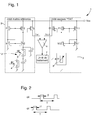
- la
figure 1 représente de manière simplifiée les différents composants du circuit électronique à référence de courant PTAT auto-calibrée selon l'invention, et - la
figure 2 représente un graphique des signaux de cadencement des commutateurs en liaison à au moins un condensateur pour l'unité maître référence du circuit électronique à référence de courant PTAT auto-calibrée selon l'invention.
- the
figure 1 represents in a simplified manner the various components of the self-calibrated PTAT current reference electronic circuit according to the invention, and - the
figure 2 represents a graph of the timing signals of the switches in connection with at least one capacitor for the reference master unit of the self-calibrated PTAT current reference electronic circuit according to the invention.
Dans la description suivante, tous les composants électroniques du circuit électronique à référence de courant PTAT, qui sont bien connus d'un homme du métier dans ce domaine technique, ne sont décrits que de manière simplifiée.In the following description, all the electronic components of the PTAT current reference electronic circuit, which are well known to those skilled in the art, are only described in a simplified manner.
A la
Pour adapter le courant de sortie PTAT IOUT, une comparaison dans un comparateur 6 est effectuée entre le courant de référence Iref de calibration de l'unité maître 2 et le courant de sortie PTAT IOUT de l'unité esclave 3. Dans un cas idéal ou après calibration, le courant de sortie PTAT IOUT est identique au courant de référence Iref. Cependant comme le circuit électronique avec la résistance 8 est intégré dans un substrat semiconducteur, tel qu'un substrat en silicium, la valeur résistive de la résistance 8 à la sortie du procédé de fabrication de type MOS n'est pas précise. De ce fait, le courant de sortie PTAT IOUT n'est pas identique au courant Iref. Dans ces conditions, la résistance programmable 8 est adaptée numériquement. La résistance programmable 8 peut être adaptée pour devenir équivalente à la résistance à condensateur commuté 12. En fonction de la comparaison entre les deux courants, une information en sortie du comparateur 6 est fournie à une unité de traitement 7 de manière à commander une adaptation numérique de la résistance programmable 8.To adapt the output current PTAT I OUT , a comparison in a
Cette résistance programmable 8 peut être composée d'un réseau de résistances et de commutateurs programmables. Le réseau de résistances comprend plusieurs résistances de valeur unitaire en série et/ou également en partie en parallèle. Dans le cas de résistances unitaires en série, des commutateurs peuvent être prévus en étant connectés en parallèle de chaque résistance unitaire ou de groupes de résistances unitaires, ce qui est bien connu. Les commutateurs sont commandés par des signaux numériques ou un mot binaire de commande provenant de l'unité de traitement 7 de manière à court-circuiter un certain nombre de résistances unitaires pour adapter la valeur résistive de la résistance programmable 8.This
L'unité de traitement 7 fournit donc un mot binaire pour commander les commutateurs et adapter la résistance programmable. Il peut être prévu un mot binaire de commande par exemple sur 16 bits de manière à ajuster ladite résistance programmable 8. Ceci permet de garantir une précision au moins de l'ordre de ±5% par rapport à la résistance estimée, alors que sans calibration, l'erreur de la résistance programmable peut être voisine de ±30% comme susmentionné. Cependant il doit être tenu compte dans la précision des erreurs d'appariement des miroirs de courant et du comparateur de courants 6, ce qui peut réduire quelque peu la précision.The
Pour adapter la résistance programmable 8, il est de préférence utilisé un algorithme de dichotomie dans l'unité de traitement 7. Cela permet de converger rapidement vers une valeur finale de la résistance programmable. Cette adaptation est effectuée pendant un certain nombre de cycles selon l'algorithme de dichotomie. Une fois que le courant de sortie PTAT IOUT devient identique au courant de référence Iref, une mémorisation du mot binaire de programmation de la résistance programmable est effectuée notamment dans une mémoire dans l'unité de traitement 7.To adapt the
L'unité maître ou générateur de courant de référence 2 comprend tout d'abord un premier miroir de courant composé de transistors N1, N2 d'un premier type de conductivité, par exemple de transistors de type NMOS. L'unité maître 2 comprend encore un second miroir de courant composé de transistors P1, P2, P3 d'un second type de conductivité, par exemple de transistors de type PMOS. Les premier et second miroirs de courant sont montés en série entre deux bornes d'une source de tension d'alimentation VDD. Le premier miroir de courant est de préférence relié à une première borne de la source de tension, qui est dans ce cas une borne de masse, alors que le second miroir de courant est de préférence relié à une seconde borne de la source de tension, qui est la borne de potentiel haut VDD.The master unit or reference current generator 2 comprises, first of all, a first current mirror composed of transistors N1, N2 of a first type of conductivity, for example NMOS type transistors. The master unit 2 further comprises a second current mirror composed of transistors P1, P2, P3 of a second conductivity type, for example PMOS type transistors. The first and second current mirrors are connected in series between two terminals of a supply voltage source V DD . The first current mirror is preferably connected to a first terminal of the voltage source, which in this case is a ground terminal, while the second current mirror is preferably connected to a second terminal of the voltage source, which is the potential terminal high V DD .
Selon la première forme d'exécution de la
Le drain et la grille du premier transistor NMOS N1 sont reliés au drain d'un premier transistor PMOS P1 du second miroir de courant. Le drain du second transistor NMOS N2 est relié à la grille et au drain d'un second transistor PMOS P2 du second miroir de courant. La grille du premier transistor PMOS P1 est reliée à la grille du second transistor PMOS P2. Le second miroir de courant comprend encore un troisième transistor PMOS P3 monté en parallèle des premier et second transistors PMOS P1, P2. La grille du troisième transistor PMOS P3 est reliée aux grilles des premier et second transistors PMOS P1, P2. Les sources des premier, second et troisième transistors PMOS P1, P2, P3 sont connectées à la borne de potentiel haut VDD de la source de tension. Le drain du troisième transistor PMOS P3 fournit le courant de référence Iref du générateur de courant de référence 2.The drain and the gate of the first NMOS transistor N1 are connected to the drain of a first PMOS transistor P1 of the second current mirror. The drain of the second NMOS transistor N2 is connected to the gate and the drain of a second PMOS transistor P2 of the second current mirror. The gate of the first PMOS transistor P1 is connected to the gate of the second PMOS transistor P2. The second current mirror further comprises a third PMOS transistor P3 connected in parallel with the first and second PMOS transistors P1, P2. The gate of the third PMOS transistor P3 is connected to the gates of the first and second PMOS transistors P1, P2. The sources of the first, second and third PMOS transistors P1, P2, P3 are connected to the high potential terminal V DD of the voltage source. The drain of the third PMOS transistor P3 provides the reference current I ref of the reference current generator 2.
Comme une résistance à condensateur commuté 12 est reliée à la source du second transistor NMOS N2, ce transistor NMOS N2 est N fois plus grand que le premier transistor NMOS N1, qui est considéré comme un transistor unitaire. Cela signifie que le second transistor NMOS N2 est composé de N premiers transistors NMOS N1, où N est un nombre entier plus grand ou égal à 2. Il peut par exemple être choisi N = 6 de manière à avoir un second transistor N2 6 fois plus grand que le premier transistor N1 ou au moins avoir une largeur de canal MOS 6 fois plus grande que la largeur de canal MOS du premier transistor N1.Since a switched
La résistance à condensateur commuté 12 comprend donc un condensateur C, dont une première électrode est reliée à un premier commutateur 4 et à un second commutateur 5. Une seconde électrode du condensateur C est reliée à la borne de masse. Dans la technologie CMOS du procédé de fabrication du circuit électronique, ce condensateur C peut être un condensateur du type CMOS à accumulation ou un condensateur à électrode métallique à oxyde mince. Cela permet d'avoir une résistance à condensateur commuté 12 avec une précision de l'ordre de ±5%, alors qu'une résistance standard intégrée 8 est réalisée avec une précision de l'ordre de ±30%.The switched
Le premier commutateur 4 est disposé entre la première électrode du condensateur C et la borne de masse, alors que le second commutateur 5 est disposé entre la première électrode du condensateur C et la source du second transistor NMOS N2. Le premier commutateur 4 est commandé par un premier signal de commande φ1, alors que le second commutateur 5 est commandé alternativement par un second signal de commande φ2. Le premier commutateur 4 est fermé, quand le second commutateur 5 est ouvert, dans une première phase, et le premier commutateur 4 est ouvert, quand le second commutateur 5 est fermé, dans une seconde phase. Chaque commutateur peut avantageusement être réalisé au moyen d'un transistor MOS, par exemple un transistor NMOS, qui est commandé sur sa grille par le signal de commande correspondant.The
La
La résistance équivalente, obtenue par la commande des premier et second commutateurs 4 et 5 avec les premier et second signaux de commande φ1 et φ2, est égale à T/C. T est la période de chaque signal de commande et C définit la capacité du condensateur. En modifiant la période T, la valeur résistive de la résistance équivalente peut être modifiée. Cette résistance équivalente de l'unité maître 2 peut être établie avec une précision de ±5% selon le procédé de fabrication du circuit électronique intégré dans un substrat en silicium traditionnel. Cette résistance équivalente 12 peut être identique à la résistance programmable 8 adaptée numériquement dans l'unité esclave 3 après la calibration du courant PTAT.The equivalent resistance, obtained by controlling the first and
A la suite de la calibration du courant de sortie PTAT IOUT, le générateur du courant de référence 2 et la base de temps pour la fourniture des signaux de commande φ1 et φ2 peuvent être déconnectés. Uniquement le générateur du courant PTAT calibré reste fonctionnel avec une précision du courant de sortie PTAT IOUT garanti avec une précision, qui peut être d'au moins ±5% de la valeur attendue.As a result of the calibration of the output current PTAT I OUT , the generator of the reference current 2 and the time base for the supply of the control signals φ1 and φ2 can be disconnected. Only the calibrated PTAT current generator remains operational with a PTAT I OUT output current accuracy guaranteed with accuracy, which can be at least ± 5% of the expected value.
De manière similaire à l'unité maître 2, l'unité esclave PTAT 3 ou le générateur de courant PTAT 3 comprend un premier miroir de courant composé de transistors N11, N12 d'un premier type de conductivité, par exemple de transistors de type NMOS. L'unité esclave PTAT 3 comprend encore un second miroir de courant composé de transistors P11, P12, P13 d'un second type de conductivité, par exemple de transistors de type PMOS. Les premier et second miroirs de courant sont montés en série entre deux bornes d'une source de tension d'alimentation VDD. Le premier miroir de courant est de préférence relié à la première borne de la source de tension, qui est dans ce cas la borne de masse, alors que le second miroir de courant est de préférence relié à la seconde borne de la source de tension, qui est la borne de potentiel haut VDD.In a manner similar to the master unit 2, the slave unit PTAT 3 or the current generator PTAT 3 comprises a first current mirror composed of transistors N11, N12 of a first conductivity type, for example NMOS type transistors. The slave unit PTAT 3 further comprises a second current mirror composed of transistors P11, P12, P13 of a second conductivity type, for example of PMOS type transistors. The first and second current mirrors are connected in series between two terminals of a supply voltage source V DD . The first current mirror is preferably connected to the first terminal of the voltage source, which in this case is the ground terminal, while the second current mirror is preferably connected to the second terminal of the voltage source, which is the potential terminal high V DD .
Comme montré à la
Le drain et la grille, du premier transistor NMOS N11 sont reliés au drain d'un premier transistor PMOS P11 du second miroir de courant. Le drain du second transistor NMOS N12 est relié à la grille et au drain d'un second transistor PMOS P12 du second miroir de courant. La grille du premier transistor PMOS P11 est reliée à la grille du second transistor PMOS P12. Le second miroir de courant de l'unité esclave PTAT 3 comprend encore un troisième transistor PMOS P13 monté en parallèle des premier et second transistors PMOS P11, P12. La grille du troisième transistor PMOS P13 est reliée aux grilles des premier et second transistors PMOS P11, P12. Les sources des premier, second et troisième transistors PMOS P11, P12, P13 sont connectées à la borne de potentiel haut VDD de la source de tension. Le drain du troisième transistor PMOS P13 fournit le courant de sortie PTAT IOUT du générateur de courant PTAT 3.The drain and the gate of the first NMOS transistor N11 are connected to the drain of a first PMOS transistor P11 of the second current mirror. The drain of the second NMOS transistor N12 is connected to the gate and the drain of a second PMOS transistor P12 of the second current mirror. The gate of the first PMOS transistor P11 is connected to the gate of the second PMOS transistor P12. The second current mirror of the slave unit PTAT 3 further comprises a third PMOS transistor P13 connected in parallel with the first and second PMOS transistors P11, P12. The gate of the third PMOS transistor P13 is connected to the gates of the first and second PMOS transistors P11, P12. The sources of the first, second and third PMOS transistors P11, P12, P13 are connected to the high potential terminal V DD of the voltage source. The drain of the third PMOS transistor P13 provides the output current PTAT I OUT of the current generator PTAT 3.
Comme la résistance programmable 8 est reliée à la source du second transistor NMOS N12, ce transistor NMOS N2 est N' fois plus grand que le premier transistor NMOS N11, qui est considéré comme un transistor unitaire. Cela signifie que le second transistor NMOS N12 est composé de N' premiers transistors NMOS N11, où N' est un nombre entier plus grand ou égal à 2. Il peut par exemple être choisi N' = 6 comme pour le second transistor N2 de l'unité maître 2. Cela permet d'avoir un second transistor N12 6 fois plus grand que le premier transistor N11 ou au moins avoir une largeur de canal MOS 6 fois plus grande que la largeur de canal MOS du premier transistor N11. Cependant le nombre N' peut être différent du nombre N.Since the
Il est encore à noter que le troisième transistor PMOS P13 peut également être prévu M fois plus grand que le premier transistor PMOS P11 et le second transistor PMOS P12 du second miroir de courant de l'unité esclave PTAT 3. M est un nombre entier plus grand ou égal à 1. Dans le cas où M est égal à 1, la résistance programmable 8, qui a été adaptée, peut être équivalente à la résistance à condensateur commuté 12 de l'unité maître 2.It should also be noted that the third PMOS transistor P13 may also be provided M times larger than the first PMOS transistor P11 and the second PMOS transistor P12 of the second current mirror of the slave unit PTAT 3. M is an integer more greater than or equal to 1. In the case where M is equal to 1, the
Selon une variante d'exécution du circuit électronique 1 non illustrée, il peut être utilisé à la place du troisième transistor PMOS P13, un ensemble de transistors unitaires combinés avec des commutateurs contrôlés numériquement. En lieu et place d'adapter numériquement la résistance programmable 8, il peut être envisagé d'avoir une résistance 8 de valeur définie, et d'adapter numériquement un rapport dimensionnel de transistors PMOS du second miroir de courant, qui fournissent le courant de sortie PTAT IOUT. Un mot binaire d'adaptation est fourni au terme des cycles de calibration par l'algorithme de dichotomie. Ce mot binaire pour configurer l'ensemble de transistors est mémorisé dans l'unité de traitement 7.According to an alternative embodiment of the
Il peut aussi être envisagé d'inverser la structure électronique de l'unité maître 2 et de l'unité esclave 3. Le premier miroir de courant avec les transistors NMOS peut être remplacé par un premier miroir de courant avec des transistors PMOS, qui est relié à la borne de potentiel haut VDD, alors que le second miroir de courant avec les transistors PMOS peut être remplacé par un second miroir de courant avec des transistors NMOS, qui est relié à la borne de masse. Dans ce cas de figure, la résistance à condensateur commuté 12 et la résistance programmable 8 sont reliées à la borne de potentiel haut VDD.It can also be envisaged to invert the electronic structure of the master unit 2 and of the slave unit 3. The first current mirror with the NMOS transistors can be replaced by a first current mirror with PMOS transistors, which is connected to the high potential terminal V DD , while the second current mirror with the PMOS transistors can be replaced by a second current mirror with NMOS transistors, which is connected to the ground terminal. In this case, the switched
Il peut aussi être envisagé d'avoir plusieurs résistances à condensateur commuté disposés en parallèle et commandées chacune par deux signaux de commande propres à chaque résistance à condensateur commuté.It may also be envisaged to have several switched capacitor resistors arranged in parallel and each controlled by two control signals specific to each switched capacitor resistor.
A partir de la description qui vient d'être faite, plusieurs variantes de réalisation du circuit électronique à référence de courant PTAT peuvent être conçues par l'homme du métier sans sortir du cadre de l'invention définie par les revendications.From the description that has just been given, several alternative embodiments of the current reference electronic circuit PTAT can be designed by those skilled in the art without departing from the scope of the invention defined by the claims.
Claims (17)
caractérisé en ce que le circuit électronique (1) comprend en outre un générateur de courant de référence (2) dépendant d'au moins une résistance à condensateur commuté (12), pour la fourniture d'un courant de référence (Iref), et
en ce que le courant de référence (Iref) et le courant de sortie PTAT (IOUT) sont comparés dans un comparateur (6) de manière à adapter numériquement la résistance intégrée (8), qui est programmable, ou à adapter numériquement un rapport dimensionnel de transistors (P11, P12, P13) d'un miroir de courant dans le générateur du courant PTAT, pour la fourniture du courant de sortie PTAT (IOUT) adapté.Electronic circuit (1) with self-calibrated PTAT type current reference, the electronic circuit (1) comprising a PTAT current generator (3) depending on at least one integrated resistor (8) for supplying a current PTAT output (I OUT ),
characterized in that the electronic circuit (1) further comprises a reference current generator (2) dependent on at least one switched capacitor resistor (12) for supplying a reference current (I ref ), and
in that the reference current (I ref ) and the output current PTAT (I OUT ) are compared in a comparator (6) so as to digitally adapt the integrated resistor (8), which is programmable, or to digitally adapt a dimensional ratio of transistors (P11, P12, P13) of a current mirror in the PTAT current generator, for providing the adapted PTAT (I OUT ) output current.
Priority Applications (7)
| Application Number | Priority Date | Filing Date | Title |
|---|---|---|---|
| EP13198965.9A EP2887176B1 (en) | 2013-12-20 | 2013-12-20 | Electronic circuit with self-calibrated PTAT current reference, and method for operating same |
| US14/558,839 US9442509B2 (en) | 2013-12-20 | 2014-12-03 | Electronic circuit with self-calibrated PTAT current reference and method for actuating the same |
| TW103142196A TWI675275B (en) | 2013-12-20 | 2014-12-04 | Electronic circuit with self-calibrated ptat current reference and method for actuating the same |
| JP2014253730A JP5918344B2 (en) | 2013-12-20 | 2014-12-16 | Electronic circuit with self-calibrated PTAT current reference and method of operating same |
| CN201410784806.4A CN104731148B (en) | 2013-12-20 | 2014-12-17 | There is the electronic circuit of PTAT current benchmark and activate the method for this circuit |
| KR1020140184793A KR101749794B1 (en) | 2013-12-20 | 2014-12-19 | Electronic circuit with self-calibrated ptat current reference and method for actuating the same |
| HK15112380.6A HK1211715A1 (en) | 2013-12-20 | 2015-12-16 | Electronic circuit with self-calibrated ptat current reference and method for actuating the same ptat |
Applications Claiming Priority (1)
| Application Number | Priority Date | Filing Date | Title |
|---|---|---|---|
| EP13198965.9A EP2887176B1 (en) | 2013-12-20 | 2013-12-20 | Electronic circuit with self-calibrated PTAT current reference, and method for operating same |
Publications (2)
| Publication Number | Publication Date |
|---|---|
| EP2887176A1 true EP2887176A1 (en) | 2015-06-24 |
| EP2887176B1 EP2887176B1 (en) | 2022-09-14 |
Family
ID=50189474
Family Applications (1)
| Application Number | Title | Priority Date | Filing Date |
|---|---|---|---|
| EP13198965.9A Active EP2887176B1 (en) | 2013-12-20 | 2013-12-20 | Electronic circuit with self-calibrated PTAT current reference, and method for operating same |
Country Status (7)
| Country | Link |
|---|---|
| US (1) | US9442509B2 (en) |
| EP (1) | EP2887176B1 (en) |
| JP (1) | JP5918344B2 (en) |
| KR (1) | KR101749794B1 (en) |
| CN (1) | CN104731148B (en) |
| HK (1) | HK1211715A1 (en) |
| TW (1) | TWI675275B (en) |
Families Citing this family (8)
| Publication number | Priority date | Publication date | Assignee | Title |
|---|---|---|---|---|
| US10078016B2 (en) | 2016-02-10 | 2018-09-18 | Nxp Usa, Inc. | On-die temperature sensor for integrated circuit |
| CN106055009A (en) * | 2016-06-17 | 2016-10-26 | 中国科学院微电子研究所 | High-precision band-gap reference circuit |
| CN108566173A (en) * | 2018-06-11 | 2018-09-21 | 杨俊杰 | A kind of RC time constant correcting circuits using CMOS technology chip interior |
| CN109341890B (en) * | 2018-10-22 | 2021-05-14 | 安徽鸿创新能源动力有限公司 | BMS temperature acquisition system and measurement method based on NTC temperature sensor |
| US10747254B1 (en) * | 2019-09-03 | 2020-08-18 | Globalfoundries Inc. | Circuit structure for adjusting PTAT current to compensate for process variations in device transistor |
| CN113253787A (en) * | 2021-06-17 | 2021-08-13 | 苏州裕太微电子有限公司 | On-chip resistor correction circuit |
| US11962311B2 (en) | 2021-10-20 | 2024-04-16 | Samsung Electronics Co., Ltd. | Sub-sampling phase locked loop with compensated loop bandwidth and integrated circuit including the same |
| CN116795165B (en) * | 2023-07-25 | 2024-04-05 | 南京米乐为微电子科技股份有限公司 | Output regulating circuit of PTAT current source |
Citations (4)
| Publication number | Priority date | Publication date | Assignee | Title |
|---|---|---|---|---|
| US6844711B1 (en) * | 2003-04-15 | 2005-01-18 | Marvell International Ltd. | Low power and high accuracy band gap voltage circuit |
| US7076384B1 (en) * | 2004-09-29 | 2006-07-11 | Xilinx, Inc. | Method and apparatus for calibrating a current-based circuit |
| EP1712973A2 (en) * | 2005-04-12 | 2006-10-18 | St Microelectronics S.A. | Circuit generating a reference current |
| US20060276986A1 (en) * | 2005-06-06 | 2006-12-07 | Standard Microsystems Corporation | Automatic reference voltage trimming technique |
Family Cites Families (17)
| Publication number | Priority date | Publication date | Assignee | Title |
|---|---|---|---|---|
| AU2780399A (en) * | 1999-02-22 | 2000-09-14 | Rose Research, L.L.C. | Self-calibrating self-regenerative comparator circuit and method |
| US6987966B1 (en) * | 1999-10-21 | 2006-01-17 | Broadcom Corporation | Adaptive radio transceiver with polyphase calibration |
| TW476418U (en) * | 1999-11-26 | 2002-02-11 | Ind Tech Res Inst | Peak value collection and its calibration circuit |
| US6622927B2 (en) * | 2001-05-08 | 2003-09-23 | Ion E. Opris | Low voltage thermostat circuit |
| US6954059B1 (en) * | 2003-04-16 | 2005-10-11 | National Semiconductor Corporation | Method and apparatus for output voltage temperature dependence adjustment of a low voltage band gap circuit |
| JP2005128939A (en) * | 2003-10-27 | 2005-05-19 | Fujitsu Ltd | Semiconductor integrated circuit |
| US20090146751A1 (en) * | 2007-12-05 | 2009-06-11 | Mobius Microsystems, Inc. | Clock, Frequency Reference, and Other Reference Signal Generator |
| WO2005092042A2 (en) * | 2004-03-22 | 2005-10-06 | Mobius Microsystems, Inc. | Transconductance and current modulation for resonant frequency control and selection |
| CN1937045B (en) * | 2005-09-23 | 2010-10-06 | 马维尔国际贸易有限公司 | Automatic write strategy calibration system for optical drive |
| US8237492B2 (en) * | 2006-12-06 | 2012-08-07 | Broadcom Corporation | Method and system for a process sensor to compensate SOC parameters in the presence of IC process manufacturing variations |
| US8022744B2 (en) * | 2008-10-03 | 2011-09-20 | Cambridge Semiconductor Limited | Signal generator |
| US8183849B2 (en) * | 2009-05-12 | 2012-05-22 | Mediatek Inc. | Calibration apparatus and calibration method thereof |
| JP5515708B2 (en) * | 2009-12-11 | 2014-06-11 | 富士通株式会社 | Bias circuit and amplifier circuit having the same |
| US8680840B2 (en) * | 2010-02-11 | 2014-03-25 | Semiconductor Components Industries, Llc | Circuits and methods of producing a reference current or voltage |
| JP5674401B2 (en) | 2010-09-24 | 2015-02-25 | ルネサスエレクトロニクス株式会社 | Semiconductor device |
| JP2013142944A (en) * | 2012-01-07 | 2013-07-22 | Toshiba Corp | Constant current circuit |
| JP2013214915A (en) * | 2012-04-04 | 2013-10-17 | Renesas Electronics Corp | Oscillating device, semiconductor device, and method of operating oscillating device |
-
2013
- 2013-12-20 EP EP13198965.9A patent/EP2887176B1/en active Active
-
2014
- 2014-12-03 US US14/558,839 patent/US9442509B2/en active Active
- 2014-12-04 TW TW103142196A patent/TWI675275B/en active
- 2014-12-16 JP JP2014253730A patent/JP5918344B2/en active Active
- 2014-12-17 CN CN201410784806.4A patent/CN104731148B/en active Active
- 2014-12-19 KR KR1020140184793A patent/KR101749794B1/en active IP Right Grant
-
2015
- 2015-12-16 HK HK15112380.6A patent/HK1211715A1/en unknown
Patent Citations (4)
| Publication number | Priority date | Publication date | Assignee | Title |
|---|---|---|---|---|
| US6844711B1 (en) * | 2003-04-15 | 2005-01-18 | Marvell International Ltd. | Low power and high accuracy band gap voltage circuit |
| US7076384B1 (en) * | 2004-09-29 | 2006-07-11 | Xilinx, Inc. | Method and apparatus for calibrating a current-based circuit |
| EP1712973A2 (en) * | 2005-04-12 | 2006-10-18 | St Microelectronics S.A. | Circuit generating a reference current |
| US20060276986A1 (en) * | 2005-06-06 | 2006-12-07 | Standard Microsystems Corporation | Automatic reference voltage trimming technique |
Non-Patent Citations (1)
| Title |
|---|
| TALEBBEYDOKHTI N ET AL: "Constant transconductance bias circuit with an on-chip resistor", 2006 IEEE INTERNATIONAL SYMPOSIUM ON CIRCUITS AND SYSTEMS 21-24 MAY 2006 ISLAND OF KOS, GREECE, IEEE - PISCATAWAY, NJ, USA, 21 May 2006 (2006-05-21), pages 4pp - 2860, XP032458343, ISBN: 978-0-7803-9389-9, DOI: 10.1109/ISCAS.2006.1693220 * |
Also Published As
| Publication number | Publication date |
|---|---|
| EP2887176B1 (en) | 2022-09-14 |
| TW201541219A (en) | 2015-11-01 |
| KR20150073122A (en) | 2015-06-30 |
| JP2015122494A (en) | 2015-07-02 |
| US9442509B2 (en) | 2016-09-13 |
| KR101749794B1 (en) | 2017-06-21 |
| JP5918344B2 (en) | 2016-05-18 |
| US20150177772A1 (en) | 2015-06-25 |
| HK1211715A1 (en) | 2016-05-27 |
| TWI675275B (en) | 2019-10-21 |
| CN104731148B (en) | 2016-08-31 |
| CN104731148A (en) | 2015-06-24 |
Similar Documents
| Publication | Publication Date | Title |
|---|---|---|
| EP2887176A1 (en) | Electronic circuit with self-calibrated PTAT current reference, and method for operating same | |
| EP0407269B1 (en) | Integrated circuit with adjustable oscillator and frequency independent of the supply voltage | |
| EP1890122A1 (en) | Temperature sensor providing a temperature signal in digital form | |
| EP2966454A1 (en) | Method for measuring a physical parameter, and electronic circuit for implementing same | |
| FR2887650A1 (en) | CIRCUIT PROVIDING REFERENCE VOLTAGE | |
| EP0718887A1 (en) | Calibration circuit for resistors | |
| EP2015038A1 (en) | Electronic sensor with integrated thermal adjustment | |
| FR2711285A1 (en) | Method and device for controlling the pulse rate of an oscillator | |
| EP1321752A1 (en) | Temperature threshold sensor with means for testing at ambiant temperature | |
| FR2887710A1 (en) | DIFFERENTIAL PAUSE POWER SWITCH OF TRANSISTORS POWERED BY LOW VCC VOLTAGE | |
| WO2007010115A1 (en) | Reading amplifier for non-volatile memory | |
| EP1712973A2 (en) | Circuit generating a reference current | |
| EP1291817B1 (en) | Variation detection of an integrated circuit environment | |
| FR2936118A1 (en) | ANALOGUE AND IMAGEUR COUNTER INCORPORATING SUCH A COUNTER. | |
| FR2958471A1 (en) | PARALLEL ANALOG / DIGITAL CONVERSION METHOD, DEVICE USING THE SAME, AND IMAGING DETECTOR COMPRISING SUCH A DEVICE | |
| EP3667915A1 (en) | Delay circuit | |
| FR2879373A1 (en) | Integrated circuit, has calibrating circuit producing adjustment value for resistor of pair of components to compensate error on resistor and capacitor product, where value is then applied to capacitor of another pair of components | |
| EP3545621B1 (en) | Switching device of a power circuit | |
| EP0379817B1 (en) | Integrated circuit with offset correction, and process for using same | |
| EP3667914B1 (en) | Calibration of a delay circuit | |
| FR2842917A1 (en) | Equipment for adjusting an operating parameter on an analogue electronic circuit, comprises adjusting resistors to change the value of circuit resistors and control by means of logic circuit and fuses | |
| FR3052271A1 (en) | VOLTAGE SUPPRESSION DEVICE | |
| FR3018137A1 (en) | ||
| FR3106026A1 (en) | Integrated circuit comprising at least one ring oscillator and method for controlling the operation of such an oscillator | |
| FR2825802A1 (en) | Device for comparing two resistances and a system incorporating the device for compensation of integrated resistances, especially for use in CMOS integrated circuits, with adjustment for resistance variations caused by temperature |
Legal Events
| Date | Code | Title | Description |
|---|---|---|---|
| PUAI | Public reference made under article 153(3) epc to a published international application that has entered the european phase |
Free format text: ORIGINAL CODE: 0009012 |
|
| 17P | Request for examination filed |
Effective date: 20131220 |
|
| AK | Designated contracting states |
Kind code of ref document: A1 Designated state(s): AL AT BE BG CH CY CZ DE DK EE ES FI FR GB GR HR HU IE IS IT LI LT LU LV MC MK MT NL NO PL PT RO RS SE SI SK SM TR |
|
| AX | Request for extension of the european patent |
Extension state: BA ME |
|
| R17P | Request for examination filed (corrected) |
Effective date: 20160104 |
|
| RBV | Designated contracting states (corrected) |
Designated state(s): AL AT BE BG CH CY CZ DE DK EE ES FI FR GB GR HR HU IE IS IT LI LT LU LV MC MK MT NL NO PL PT RO RS SE SI SK SM TR |
|
| STAA | Information on the status of an ep patent application or granted ep patent |
Free format text: STATUS: EXAMINATION IS IN PROGRESS |
|
| 17Q | First examination report despatched |
Effective date: 20201105 |
|
| STAA | Information on the status of an ep patent application or granted ep patent |
Free format text: STATUS: EXAMINATION IS IN PROGRESS |
|
| GRAP | Despatch of communication of intention to grant a patent |
Free format text: ORIGINAL CODE: EPIDOSNIGR1 |
|
| STAA | Information on the status of an ep patent application or granted ep patent |
Free format text: STATUS: GRANT OF PATENT IS INTENDED |
|
| INTG | Intention to grant announced |
Effective date: 20220628 |
|
| GRAS | Grant fee paid |
Free format text: ORIGINAL CODE: EPIDOSNIGR3 |
|
| GRAA | (expected) grant |
Free format text: ORIGINAL CODE: 0009210 |
|
| STAA | Information on the status of an ep patent application or granted ep patent |
Free format text: STATUS: THE PATENT HAS BEEN GRANTED |
|
| AK | Designated contracting states |
Kind code of ref document: B1 Designated state(s): AL AT BE BG CH CY CZ DE DK EE ES FI FR GB GR HR HU IE IS IT LI LT LU LV MC MK MT NL NO PL PT RO RS SE SI SK SM TR |
|
| REG | Reference to a national code |
Ref country code: GB Ref legal event code: FG4D Free format text: NOT ENGLISH |
|
| REG | Reference to a national code |
Ref country code: CH Ref legal event code: EP |
|
| REG | Reference to a national code |
Ref country code: DE Ref legal event code: R096 Ref document number: 602013082504 Country of ref document: DE |
|
| REG | Reference to a national code |
Ref country code: IE Ref legal event code: FG4D Free format text: LANGUAGE OF EP DOCUMENT: FRENCH |
|
| REG | Reference to a national code |
Ref country code: AT Ref legal event code: REF Ref document number: 1519101 Country of ref document: AT Kind code of ref document: T Effective date: 20221015 |
|
| REG | Reference to a national code |
Ref country code: LT Ref legal event code: MG9D |
|
| REG | Reference to a national code |
Ref country code: NL Ref legal event code: MP Effective date: 20220914 |
|
| PG25 | Lapsed in a contracting state [announced via postgrant information from national office to epo] |
Ref country code: SE Free format text: LAPSE BECAUSE OF FAILURE TO SUBMIT A TRANSLATION OF THE DESCRIPTION OR TO PAY THE FEE WITHIN THE PRESCRIBED TIME-LIMIT Effective date: 20220914 Ref country code: RS Free format text: LAPSE BECAUSE OF FAILURE TO SUBMIT A TRANSLATION OF THE DESCRIPTION OR TO PAY THE FEE WITHIN THE PRESCRIBED TIME-LIMIT Effective date: 20220914 Ref country code: NO Free format text: LAPSE BECAUSE OF FAILURE TO SUBMIT A TRANSLATION OF THE DESCRIPTION OR TO PAY THE FEE WITHIN THE PRESCRIBED TIME-LIMIT Effective date: 20221214 Ref country code: LV Free format text: LAPSE BECAUSE OF FAILURE TO SUBMIT A TRANSLATION OF THE DESCRIPTION OR TO PAY THE FEE WITHIN THE PRESCRIBED TIME-LIMIT Effective date: 20220914 Ref country code: LT Free format text: LAPSE BECAUSE OF FAILURE TO SUBMIT A TRANSLATION OF THE DESCRIPTION OR TO PAY THE FEE WITHIN THE PRESCRIBED TIME-LIMIT Effective date: 20220914 Ref country code: FI Free format text: LAPSE BECAUSE OF FAILURE TO SUBMIT A TRANSLATION OF THE DESCRIPTION OR TO PAY THE FEE WITHIN THE PRESCRIBED TIME-LIMIT Effective date: 20220914 |
|
| REG | Reference to a national code |
Ref country code: AT Ref legal event code: MK05 Ref document number: 1519101 Country of ref document: AT Kind code of ref document: T Effective date: 20220914 |
|
| PG25 | Lapsed in a contracting state [announced via postgrant information from national office to epo] |
Ref country code: HR Free format text: LAPSE BECAUSE OF FAILURE TO SUBMIT A TRANSLATION OF THE DESCRIPTION OR TO PAY THE FEE WITHIN THE PRESCRIBED TIME-LIMIT Effective date: 20220914 Ref country code: GR Free format text: LAPSE BECAUSE OF FAILURE TO SUBMIT A TRANSLATION OF THE DESCRIPTION OR TO PAY THE FEE WITHIN THE PRESCRIBED TIME-LIMIT Effective date: 20221215 |
|
| PG25 | Lapsed in a contracting state [announced via postgrant information from national office to epo] |
Ref country code: SM Free format text: LAPSE BECAUSE OF FAILURE TO SUBMIT A TRANSLATION OF THE DESCRIPTION OR TO PAY THE FEE WITHIN THE PRESCRIBED TIME-LIMIT Effective date: 20220914 Ref country code: RO Free format text: LAPSE BECAUSE OF FAILURE TO SUBMIT A TRANSLATION OF THE DESCRIPTION OR TO PAY THE FEE WITHIN THE PRESCRIBED TIME-LIMIT Effective date: 20220914 Ref country code: PT Free format text: LAPSE BECAUSE OF FAILURE TO SUBMIT A TRANSLATION OF THE DESCRIPTION OR TO PAY THE FEE WITHIN THE PRESCRIBED TIME-LIMIT Effective date: 20230116 Ref country code: ES Free format text: LAPSE BECAUSE OF FAILURE TO SUBMIT A TRANSLATION OF THE DESCRIPTION OR TO PAY THE FEE WITHIN THE PRESCRIBED TIME-LIMIT Effective date: 20220914 Ref country code: CZ Free format text: LAPSE BECAUSE OF FAILURE TO SUBMIT A TRANSLATION OF THE DESCRIPTION OR TO PAY THE FEE WITHIN THE PRESCRIBED TIME-LIMIT Effective date: 20220914 Ref country code: AT Free format text: LAPSE BECAUSE OF FAILURE TO SUBMIT A TRANSLATION OF THE DESCRIPTION OR TO PAY THE FEE WITHIN THE PRESCRIBED TIME-LIMIT Effective date: 20220914 |
|
| PGFP | Annual fee paid to national office [announced via postgrant information from national office to epo] |
Ref country code: CH Payment date: 20230101 Year of fee payment: 10 |
|
| PG25 | Lapsed in a contracting state [announced via postgrant information from national office to epo] |
Ref country code: SK Free format text: LAPSE BECAUSE OF FAILURE TO SUBMIT A TRANSLATION OF THE DESCRIPTION OR TO PAY THE FEE WITHIN THE PRESCRIBED TIME-LIMIT Effective date: 20220914 Ref country code: PL Free format text: LAPSE BECAUSE OF FAILURE TO SUBMIT A TRANSLATION OF THE DESCRIPTION OR TO PAY THE FEE WITHIN THE PRESCRIBED TIME-LIMIT Effective date: 20220914 Ref country code: IS Free format text: LAPSE BECAUSE OF FAILURE TO SUBMIT A TRANSLATION OF THE DESCRIPTION OR TO PAY THE FEE WITHIN THE PRESCRIBED TIME-LIMIT Effective date: 20230114 Ref country code: EE Free format text: LAPSE BECAUSE OF FAILURE TO SUBMIT A TRANSLATION OF THE DESCRIPTION OR TO PAY THE FEE WITHIN THE PRESCRIBED TIME-LIMIT Effective date: 20220914 |
|
| REG | Reference to a national code |
Ref country code: DE Ref legal event code: R097 Ref document number: 602013082504 Country of ref document: DE |
|
| PG25 | Lapsed in a contracting state [announced via postgrant information from national office to epo] |
Ref country code: NL Free format text: LAPSE BECAUSE OF FAILURE TO SUBMIT A TRANSLATION OF THE DESCRIPTION OR TO PAY THE FEE WITHIN THE PRESCRIBED TIME-LIMIT Effective date: 20220914 Ref country code: AL Free format text: LAPSE BECAUSE OF FAILURE TO SUBMIT A TRANSLATION OF THE DESCRIPTION OR TO PAY THE FEE WITHIN THE PRESCRIBED TIME-LIMIT Effective date: 20220914 |
|
| PLBE | No opposition filed within time limit |
Free format text: ORIGINAL CODE: 0009261 |
|
| STAA | Information on the status of an ep patent application or granted ep patent |
Free format text: STATUS: NO OPPOSITION FILED WITHIN TIME LIMIT |
|
| P01 | Opt-out of the competence of the unified patent court (upc) registered |
Effective date: 20230615 |
|
| PG25 | Lapsed in a contracting state [announced via postgrant information from national office to epo] |
Ref country code: DK Free format text: LAPSE BECAUSE OF FAILURE TO SUBMIT A TRANSLATION OF THE DESCRIPTION OR TO PAY THE FEE WITHIN THE PRESCRIBED TIME-LIMIT Effective date: 20220914 |
|
| 26N | No opposition filed |
Effective date: 20230615 |
|
| GBPC | Gb: european patent ceased through non-payment of renewal fee |
Effective date: 20221220 |
|
| REG | Reference to a national code |
Ref country code: BE Ref legal event code: MM Effective date: 20221231 |
|
| PG25 | Lapsed in a contracting state [announced via postgrant information from national office to epo] |
Ref country code: SI Free format text: LAPSE BECAUSE OF FAILURE TO SUBMIT A TRANSLATION OF THE DESCRIPTION OR TO PAY THE FEE WITHIN THE PRESCRIBED TIME-LIMIT Effective date: 20220914 Ref country code: LU Free format text: LAPSE BECAUSE OF NON-PAYMENT OF DUE FEES Effective date: 20221220 |
|
| PG25 | Lapsed in a contracting state [announced via postgrant information from national office to epo] |
Ref country code: IE Free format text: LAPSE BECAUSE OF NON-PAYMENT OF DUE FEES Effective date: 20221220 Ref country code: GB Free format text: LAPSE BECAUSE OF NON-PAYMENT OF DUE FEES Effective date: 20221220 |
|
| PG25 | Lapsed in a contracting state [announced via postgrant information from national office to epo] |
Ref country code: BE Free format text: LAPSE BECAUSE OF NON-PAYMENT OF DUE FEES Effective date: 20221231 |
|
| PGFP | Annual fee paid to national office [announced via postgrant information from national office to epo] |
Ref country code: FR Payment date: 20231122 Year of fee payment: 11 Ref country code: DE Payment date: 20231121 Year of fee payment: 11 |
|
| PG25 | Lapsed in a contracting state [announced via postgrant information from national office to epo] |
Ref country code: HU Free format text: LAPSE BECAUSE OF FAILURE TO SUBMIT A TRANSLATION OF THE DESCRIPTION OR TO PAY THE FEE WITHIN THE PRESCRIBED TIME-LIMIT; INVALID AB INITIO Effective date: 20131220 |