EP2884592B1 - Elektrisches Verbindungssystem - Google Patents
Elektrisches Verbindungssystem Download PDFInfo
- Publication number
- EP2884592B1 EP2884592B1 EP14196316.5A EP14196316A EP2884592B1 EP 2884592 B1 EP2884592 B1 EP 2884592B1 EP 14196316 A EP14196316 A EP 14196316A EP 2884592 B1 EP2884592 B1 EP 2884592B1
- Authority
- EP
- European Patent Office
- Prior art keywords
- receptacle
- plug
- shield
- terminals
- terminal
- Prior art date
- Legal status (The legal status is an assumption and is not a legal conclusion. Google has not performed a legal analysis and makes no representation as to the accuracy of the status listed.)
- Active
Links
- 239000004020 conductor Substances 0.000 claims description 100
- 239000003989 dielectric material Substances 0.000 claims description 9
- 238000000926 separation method Methods 0.000 claims description 7
- 230000002146 bilateral effect Effects 0.000 claims description 4
- 230000008878 coupling Effects 0.000 claims description 3
- 238000010168 coupling process Methods 0.000 claims description 3
- 238000005859 coupling reaction Methods 0.000 claims description 3
- 230000003247 decreasing effect Effects 0.000 claims description 2
- 239000012212 insulator Substances 0.000 description 27
- RYGMFSIKBFXOCR-UHFFFAOYSA-N Copper Chemical compound [Cu] RYGMFSIKBFXOCR-UHFFFAOYSA-N 0.000 description 22
- 229910052802 copper Inorganic materials 0.000 description 18
- 239000010949 copper Substances 0.000 description 18
- 238000000034 method Methods 0.000 description 14
- 230000008569 process Effects 0.000 description 13
- 238000012546 transfer Methods 0.000 description 10
- BQCADISMDOOEFD-UHFFFAOYSA-N Silver Chemical compound [Ag] BQCADISMDOOEFD-UHFFFAOYSA-N 0.000 description 9
- 230000008901 benefit Effects 0.000 description 9
- 238000003780 insertion Methods 0.000 description 9
- 230000037431 insertion Effects 0.000 description 9
- 229910052709 silver Inorganic materials 0.000 description 9
- 239000004332 silver Substances 0.000 description 9
- 239000007787 solid Substances 0.000 description 9
- ATJFFYVFTNAWJD-UHFFFAOYSA-N Tin Chemical compound [Sn] ATJFFYVFTNAWJD-UHFFFAOYSA-N 0.000 description 8
- 238000010276 construction Methods 0.000 description 7
- 239000000463 material Substances 0.000 description 6
- 239000000835 fiber Substances 0.000 description 5
- 238000009413 insulation Methods 0.000 description 5
- 230000000670 limiting effect Effects 0.000 description 5
- 229920002799 BoPET Polymers 0.000 description 4
- PXHVJJICTQNCMI-UHFFFAOYSA-N Nickel Chemical compound [Ni] PXHVJJICTQNCMI-UHFFFAOYSA-N 0.000 description 4
- 238000013461 design Methods 0.000 description 4
- 238000003466 welding Methods 0.000 description 4
- 229920000106 Liquid crystal polymer Polymers 0.000 description 3
- 239000004977 Liquid-crystal polymers (LCPs) Substances 0.000 description 3
- 229920000134 Metallised film Polymers 0.000 description 3
- 229910045601 alloy Inorganic materials 0.000 description 3
- 239000000956 alloy Substances 0.000 description 3
- 230000005540 biological transmission Effects 0.000 description 3
- 238000004891 communication Methods 0.000 description 3
- 238000002788 crimping Methods 0.000 description 3
- 230000007613 environmental effect Effects 0.000 description 3
- 238000007373 indentation Methods 0.000 description 3
- 238000000465 moulding Methods 0.000 description 3
- 238000007747 plating Methods 0.000 description 3
- -1 polypropylene Polymers 0.000 description 3
- 238000005299 abrasion Methods 0.000 description 2
- 238000005094 computer simulation Methods 0.000 description 2
- 230000000694 effects Effects 0.000 description 2
- 230000036039 immunity Effects 0.000 description 2
- 230000002401 inhibitory effect Effects 0.000 description 2
- 238000005304 joining Methods 0.000 description 2
- 238000004519 manufacturing process Methods 0.000 description 2
- 230000007246 mechanism Effects 0.000 description 2
- 229910052759 nickel Inorganic materials 0.000 description 2
- 229920000728 polyester Polymers 0.000 description 2
- 230000007704 transition Effects 0.000 description 2
- 239000005041 Mylar™ Substances 0.000 description 1
- 239000004952 Polyamide Substances 0.000 description 1
- 239000004698 Polyethylene Substances 0.000 description 1
- 239000004743 Polypropylene Substances 0.000 description 1
- 230000001154 acute effect Effects 0.000 description 1
- XAGFODPZIPBFFR-UHFFFAOYSA-N aluminium Chemical compound [Al] XAGFODPZIPBFFR-UHFFFAOYSA-N 0.000 description 1
- 229910052782 aluminium Inorganic materials 0.000 description 1
- 238000005452 bending Methods 0.000 description 1
- 230000015572 biosynthetic process Effects 0.000 description 1
- 239000003795 chemical substances by application Substances 0.000 description 1
- 239000011248 coating agent Substances 0.000 description 1
- 238000000576 coating method Methods 0.000 description 1
- 229920003020 cross-linked polyethylene Polymers 0.000 description 1
- 239000004703 cross-linked polyethylene Substances 0.000 description 1
- 230000001419 dependent effect Effects 0.000 description 1
- 230000000881 depressing effect Effects 0.000 description 1
- 238000010292 electrical insulation Methods 0.000 description 1
- 229920006351 engineering plastic Polymers 0.000 description 1
- 239000000446 fuel Substances 0.000 description 1
- 239000010410 layer Substances 0.000 description 1
- 230000013011 mating Effects 0.000 description 1
- 230000036961 partial effect Effects 0.000 description 1
- 230000035699 permeability Effects 0.000 description 1
- 229920002647 polyamide Polymers 0.000 description 1
- 229920001707 polybutylene terephthalate Polymers 0.000 description 1
- 229920000573 polyethylene Polymers 0.000 description 1
- 229920001155 polypropylene Polymers 0.000 description 1
- 239000000843 powder Substances 0.000 description 1
- 238000012545 processing Methods 0.000 description 1
- 230000008054 signal transmission Effects 0.000 description 1
- 239000002356 single layer Substances 0.000 description 1
- 229910000679 solder Inorganic materials 0.000 description 1
- 238000005476 soldering Methods 0.000 description 1
- 125000006850 spacer group Chemical group 0.000 description 1
- 239000000454 talc Substances 0.000 description 1
- 229910052623 talc Inorganic materials 0.000 description 1
Images


Classifications
-
- H—ELECTRICITY
- H01—ELECTRIC ELEMENTS
- H01R—ELECTRICALLY-CONDUCTIVE CONNECTIONS; STRUCTURAL ASSOCIATIONS OF A PLURALITY OF MUTUALLY-INSULATED ELECTRICAL CONNECTING ELEMENTS; COUPLING DEVICES; CURRENT COLLECTORS
- H01R13/00—Details of coupling devices of the kinds covered by groups H01R12/70 or H01R24/00 - H01R33/00
- H01R13/46—Bases; Cases
-
- H—ELECTRICITY
- H01—ELECTRIC ELEMENTS
- H01R—ELECTRICALLY-CONDUCTIVE CONNECTIONS; STRUCTURAL ASSOCIATIONS OF A PLURALITY OF MUTUALLY-INSULATED ELECTRICAL CONNECTING ELEMENTS; COUPLING DEVICES; CURRENT COLLECTORS
- H01R13/00—Details of coupling devices of the kinds covered by groups H01R12/70 or H01R24/00 - H01R33/00
- H01R13/02—Contact members
- H01R13/26—Pin or blade contacts for sliding co-operation on one side only
-
- H—ELECTRICITY
- H01—ELECTRIC ELEMENTS
- H01R—ELECTRICALLY-CONDUCTIVE CONNECTIONS; STRUCTURAL ASSOCIATIONS OF A PLURALITY OF MUTUALLY-INSULATED ELECTRICAL CONNECTING ELEMENTS; COUPLING DEVICES; CURRENT COLLECTORS
- H01R13/00—Details of coupling devices of the kinds covered by groups H01R12/70 or H01R24/00 - H01R33/00
- H01R13/62—Means for facilitating engagement or disengagement of coupling parts or for holding them in engagement
- H01R13/627—Snap or like fastening
-
- H—ELECTRICITY
- H01—ELECTRIC ELEMENTS
- H01R—ELECTRICALLY-CONDUCTIVE CONNECTIONS; STRUCTURAL ASSOCIATIONS OF A PLURALITY OF MUTUALLY-INSULATED ELECTRICAL CONNECTING ELEMENTS; COUPLING DEVICES; CURRENT COLLECTORS
- H01R24/00—Two-part coupling devices, or either of their cooperating parts, characterised by their overall structure
- H01R24/28—Coupling parts carrying pins, blades or analogous contacts and secured only to wire or cable
-
- H—ELECTRICITY
- H01—ELECTRIC ELEMENTS
- H01R—ELECTRICALLY-CONDUCTIVE CONNECTIONS; STRUCTURAL ASSOCIATIONS OF A PLURALITY OF MUTUALLY-INSULATED ELECTRICAL CONNECTING ELEMENTS; COUPLING DEVICES; CURRENT COLLECTORS
- H01R13/00—Details of coupling devices of the kinds covered by groups H01R12/70 or H01R24/00 - H01R33/00
- H01R13/40—Securing contact members in or to a base or case; Insulating of contact members
- H01R13/42—Securing in a demountable manner
- H01R13/428—Securing in a demountable manner by resilient locking means on the contact members; by locking means on resilient contact members
- H01R13/432—Securing in a demountable manner by resilient locking means on the contact members; by locking means on resilient contact members by stamped-out resilient tongue snapping behind shoulder in base or case
-
- H—ELECTRICITY
- H01—ELECTRIC ELEMENTS
- H01R—ELECTRICALLY-CONDUCTIVE CONNECTIONS; STRUCTURAL ASSOCIATIONS OF A PLURALITY OF MUTUALLY-INSULATED ELECTRICAL CONNECTING ELEMENTS; COUPLING DEVICES; CURRENT COLLECTORS
- H01R13/00—Details of coupling devices of the kinds covered by groups H01R12/70 or H01R24/00 - H01R33/00
- H01R13/46—Bases; Cases
- H01R13/50—Bases; Cases formed as an integral body
-
- H—ELECTRICITY
- H01—ELECTRIC ELEMENTS
- H01R—ELECTRICALLY-CONDUCTIVE CONNECTIONS; STRUCTURAL ASSOCIATIONS OF A PLURALITY OF MUTUALLY-INSULATED ELECTRICAL CONNECTING ELEMENTS; COUPLING DEVICES; CURRENT COLLECTORS
- H01R13/00—Details of coupling devices of the kinds covered by groups H01R12/70 or H01R24/00 - H01R33/00
- H01R13/648—Protective earth or shield arrangements on coupling devices, e.g. anti-static shielding
- H01R13/658—High frequency shielding arrangements, e.g. against EMI [Electro-Magnetic Interference] or EMP [Electro-Magnetic Pulse]
- H01R13/6581—Shield structure
- H01R13/6582—Shield structure with resilient means for engaging mating connector
-
- H—ELECTRICITY
- H01—ELECTRIC ELEMENTS
- H01R—ELECTRICALLY-CONDUCTIVE CONNECTIONS; STRUCTURAL ASSOCIATIONS OF A PLURALITY OF MUTUALLY-INSULATED ELECTRICAL CONNECTING ELEMENTS; COUPLING DEVICES; CURRENT COLLECTORS
- H01R2103/00—Two poles
-
- H—ELECTRICITY
- H01—ELECTRIC ELEMENTS
- H01R—ELECTRICALLY-CONDUCTIVE CONNECTIONS; STRUCTURAL ASSOCIATIONS OF A PLURALITY OF MUTUALLY-INSULATED ELECTRICAL CONNECTING ELEMENTS; COUPLING DEVICES; CURRENT COLLECTORS
- H01R4/00—Electrically-conductive connections between two or more conductive members in direct contact, i.e. touching one another; Means for effecting or maintaining such contact; Electrically-conductive connections having two or more spaced connecting locations for conductors and using contact members penetrating insulation
- H01R4/10—Electrically-conductive connections between two or more conductive members in direct contact, i.e. touching one another; Means for effecting or maintaining such contact; Electrically-conductive connections having two or more spaced connecting locations for conductors and using contact members penetrating insulation effected solely by twisting, wrapping, bending, crimping, or other permanent deformation
- H01R4/18—Electrically-conductive connections between two or more conductive members in direct contact, i.e. touching one another; Means for effecting or maintaining such contact; Electrically-conductive connections having two or more spaced connecting locations for conductors and using contact members penetrating insulation effected solely by twisting, wrapping, bending, crimping, or other permanent deformation by crimping
- H01R4/183—Electrically-conductive connections between two or more conductive members in direct contact, i.e. touching one another; Means for effecting or maintaining such contact; Electrically-conductive connections having two or more spaced connecting locations for conductors and using contact members penetrating insulation effected solely by twisting, wrapping, bending, crimping, or other permanent deformation by crimping for cylindrical elongated bodies, e.g. cables having circular cross-section
- H01R4/184—Electrically-conductive connections between two or more conductive members in direct contact, i.e. touching one another; Means for effecting or maintaining such contact; Electrically-conductive connections having two or more spaced connecting locations for conductors and using contact members penetrating insulation effected solely by twisting, wrapping, bending, crimping, or other permanent deformation by crimping for cylindrical elongated bodies, e.g. cables having circular cross-section comprising a U-shaped wire-receiving portion
- H01R4/185—Electrically-conductive connections between two or more conductive members in direct contact, i.e. touching one another; Means for effecting or maintaining such contact; Electrically-conductive connections having two or more spaced connecting locations for conductors and using contact members penetrating insulation effected solely by twisting, wrapping, bending, crimping, or other permanent deformation by crimping for cylindrical elongated bodies, e.g. cables having circular cross-section comprising a U-shaped wire-receiving portion combined with a U-shaped insulation-receiving portion
-
- H—ELECTRICITY
- H01—ELECTRIC ELEMENTS
- H01R—ELECTRICALLY-CONDUCTIVE CONNECTIONS; STRUCTURAL ASSOCIATIONS OF A PLURALITY OF MUTUALLY-INSULATED ELECTRICAL CONNECTING ELEMENTS; COUPLING DEVICES; CURRENT COLLECTORS
- H01R9/00—Structural associations of a plurality of mutually-insulated electrical connecting elements, e.g. terminal strips or terminal blocks; Terminals or binding posts mounted upon a base or in a case; Bases therefor
- H01R9/03—Connectors arranged to contact a plurality of the conductors of a multiconductor cable, e.g. tapping connections
- H01R9/05—Connectors arranged to contact a plurality of the conductors of a multiconductor cable, e.g. tapping connections for coaxial cables
- H01R9/0518—Connection to outer conductor by crimping or by crimping ferrule
-
- H—ELECTRICITY
- H01—ELECTRIC ELEMENTS
- H01R—ELECTRICALLY-CONDUCTIVE CONNECTIONS; STRUCTURAL ASSOCIATIONS OF A PLURALITY OF MUTUALLY-INSULATED ELECTRICAL CONNECTING ELEMENTS; COUPLING DEVICES; CURRENT COLLECTORS
- H01R9/00—Structural associations of a plurality of mutually-insulated electrical connecting elements, e.g. terminal strips or terminal blocks; Terminals or binding posts mounted upon a base or in a case; Bases therefor
- H01R9/03—Connectors arranged to contact a plurality of the conductors of a multiconductor cable, e.g. tapping connections
- H01R9/05—Connectors arranged to contact a plurality of the conductors of a multiconductor cable, e.g. tapping connections for coaxial cables
- H01R9/053—Connectors arranged to contact a plurality of the conductors of a multiconductor cable, e.g. tapping connections for coaxial cables using contact members penetrating insulation
Definitions
- the invention generally relates to an electrical connection system, and more particularly relates to an electrical connection system designed to connect wire cables transmitting digital electrical signals having a data transfer rate of 5 Gigabits per second (Gb/s) or higher.
- Transmission media used to connect electronic components to the digital data processors must be constructed to efficiently transmit the high speed digital signals between the various components.
- Wired media such as fiber optic cable, coaxial cable, or twisted pair cable may be suitable in applications where the components being connected are in fixed locations and are relatively close proximity, e.g. separated by less than 100 meters.
- Fiber optic cable provides a transmission medium that can support data rates of up to nearly 100 Gb/s and is practically immune to electromagnetic interference.
- Coaxial cable typically supports data transfer rates up to 100 Megabits per second (Mb/s) and has good immunity to electromagnetic interference.
- Twisted pair cable can support data rates of up to about 5 Gb/s, although these cables typically require multiple twisted pairs within the cable dedicated to transmit or receive lines.
- the conductors of the twisted pair cables offer good resistance to electromagnetic interference which can be improved by including shielding for the twisted pairs within the cable.
- USB Universal Serial Bus
- HDMI High Definition Multimedia Interface
- Infotainment systems and other electronic systems in automobiles and trucks are beginning to require cables capable of carrying high data rate signals.
- Automotive grade cables must not only be able to meet environmental requirements (e.g. thermal and moisture resistance), they must also be flexible enough to be routed in a vehicle wiring harness and have a low mass to help meet vehicle fuel economy requirements. Therefore, there is a need for a wire cable with a high data transfer rate that has low mass and is flexible enough to be packaged within a vehicle wiring harness, while meeting cost targets that cannot currently be met by fiber optic cable.
- this wire cable is automotive, such a wire cable would also likely find other applications, such as aerospace, industrial control, or other data communications.
- the wire cable assembly includes a wire cable having a pair of conductors (wire pair) and a conductive sheet and braided conductor to isolate the wire pair from electromagnetic interference and determine the characteristic impedance of the cable.
- the wire pair is encased within dielectric belting that helps to provide a consistent radial distance between the wire pair and the shield.
- the belting may also help to maintain a consistent twist angle between the wire pair if they are twisted.
- the consistent radial distance between the wire pair and the shield and the consistent twist angle provides a wire cable with more consistent impedance.
- the wire cable assembly may also include an electrical receptacle connector having a mirrored pair of plug terminals connected to the wire pair and/or an electrical plug connector having a mirrored pair of receptacle terminals connected to the wire pair that is configured to mate with the plug terminals of the plug connector.
- the receptacle and plug terminals each have a generally rectangular cross section and when the first and second electrical connectors are mated, the major widths of the receptacle terminals are substantially perpendicular to the major widths of the plug terminals and the contact points between the receptacle and plug terminals are external to the receptacle and plug terminals.
- Both the receptacle and plug connectors include a shield that longitudinally surrounds the receptacle or plug terminals and is connected to the braided conductor of the wire cable.
- the wire cable assembly may also include an insulative connector body that contains the receptacle or plug terminals and shield.
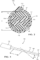
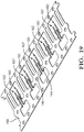
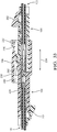
- Figs. 1 and 2 illustrate a non-limiting example of a wire cable 100a used in the wire cable assembly.
- the wire cable 100a includes a central pair of conductors comprising a first inner conductor, hereinafter referred to as the first conductor 102a and a second inner conductor, hereinafter referred to as the second conductor 104a.
- the first and second conductors 102a, 104a are formed of a conductive material with superior conductivity, such as unplated copper or silver plated copper.
- copper refers to elemental copper or a copper-based alloy.
- silver refers to elemental silver or a silver-based alloy.
- the first and second conductors 102a, 104a if wire cable 100a may each consist of seven wire strands 106.
- Each of the wire strands 106 of the first and second conductors 102a, 104a may be characterized as having a diameter of 0.12 millimeters (mm), which is generally equivalent to 28 American Wire Gauge (AWG) stranded wire.
- AWG American Wire Gauge
- the first and second conductors 102a, 104a may be formed of stranded wire having a smaller gauge, such as 30 AWG or 32 AWG.
- the central pair of first and second conductors 102a, 104a is longitudinally twisted over a length L, for example once every 8.89 mm. Twisting the first and second conductors 102a, 104a provides the benefit of reducing low frequency electromagnetic interference of the signal carried by the central pair.
- satisfactory signal transmission performance may also be provided by a wire cable wherein the first and second conductors 102a, 104a are not twisted about one about the other. Not twisting the first and second conductors 102a, 104a may provide the benefit of reducing manufacturing cost of the wire cable by eliminating the twisting process.
- each of the first and second conductors 102a, 104a are enclosed within a respective first dielectric insulator and a second dielectric insulator, hereafter referred to as the first and second insulators 108, 110.
- the first and second insulators 108, 110 are bonded together.
- the first and second insulators 108, 110 run the entire length of the wire cable 100a, except for portions that are removed at the ends of the cable in order to terminate the wire cable 100a.
- the first and second insulators 108, 110 are formed of a flexible dielectric material, such as polypropylene.
- the first and second insulators 108, 110 may be characterized as having a thickness of about 0.85 mm.
- Bonding the first insulator 108 to the second insulators 110 helps to maintain the spacing between the first and second conductors 102a, 104a. It may also keep a twist angle ⁇ (see Fig. 3 ) between the first and second conductors 102a, 104a consistent when the first and second conductors 102a, 104a are twisted.
- the methods required to manufacture a pair of conductors with bonded insulators are well known to those skilled in the art.
- the first and second conductors 102a, 104a and the first and second insulators 108, 110 are completely enclosed within a third dielectric insulator, hereafter referred to as the belting 112, except for portions that are removed at the ends of the cable in order to terminate the wire cable 100a.
- the first and second insulators 108, 110 and the belting 112 together form a dielectric structure 113.
- the belting 112 is formed of a flexible dielectric material, such as polyethylene. As illustrated in Fig. 2 , the belting may be characterized as having a diameter D of 2.22 mm.
- a release agent 114 such as a talc-based powder, may be applied to an outer surface of the bonded first and second insulators 108, 110 in order to facilitate removal of the belting 112 from the first and second insulators 108, 110 when ends of the first and second insulators 108, 110 are stripped from the first and second conductors 102a, 104a to form terminations of the wire cable 100a.
- the belting 112 is completely enclosed within a conductive sheet, hereafter referred to as the inner shield 116, except for portions that may be removed at the ends of the cable in order to terminate the wire cable 100a.
- the inner shield 116 is longitudinally wrapped in a single layer about the belting 112, so that it forms a single seam 118 that runs generally parallel to the central pair of first and second conductors 102a, 104a.
- the inner shield 116 is not spirally wrapped or helically wrapped about the belting 112.
- the seam edges of the inner shield 116 may overlap, so that the inner shield 116 covers at least 100 percent of an outer surface of the belting 112.
- the inner shield 116 is formed of a flexible conductive material, such as aluminized biaxially oriented PET film.
- Biaxially oriented polyethylene terephthalate film is commonly known by the trade name MYLAR and the aluminized biaxially oriented PET film will hereafter be referred to as aluminized MYLAR film.
- the aluminized MYLAR film has a conductive aluminum coating applied to only one of the major surfaces; the other major surface is non-aluminized and therefore non-conductive.
- the design, construction, and sources for single-sided aluminized MYLAR films are well known to those skilled in the art.
- the non- aluminized surface of the inner shield 116 is in contact with an outer surface of the belting 112.
- the inner shield 116 may be characterized as having a thickness of less than or equal to 0.04 mm.
- the belting 112 provides the advantage of maintaining a consistent radial distance between the first and second conductor 102a, 104a and the inner shield 116.
- the belting 112 further provides an advantage of keeping the twist angle ⁇ of the first and second conductors 102a, 104a consistent. Shielded twisted pair cables found in the prior art typically only have air as a dielectric between the twisted pair and the shield. Both the distance between first and second conductors 102a, 104a and the inner shield 116 and the effective twist angle ⁇ of the first and second conductors 102a, 104a affect the wire cable impedance.
- a wire cable with more consistent radial distance between the first and second conductors 102a, 104a and the inner shield 116 provides more consistent impedance.
- a more consistent twist angle ⁇ of the first and second conductors 102a, 104a also provides more consistent impedance.
- a wire cable may be envisioned incorporating a single dielectric structure encasing the first and second insulators to maintain a consistent lateral distance between the first and second insulators and a consistent radial distance between the first and second insulators and the inner shield.
- the dielectric structure may also keep the twist angle ⁇ of the first and second conductors consistent.
- the wire cable 100a additionally includes a ground conductor, hereafter referred to as the drain wire 120a that is disposed outside of the inner shield 116.
- the drain wire 120a extends generally parallel to the first and second conductors 102a, 104a and is in intimate contact or at least in electrical communication with the aluminized outer surface of the inner shield 116.
- the drain wire 120a of wire cable 100a may consist of seven wire strands 122.
- Each of the wire strands 122 of the drain wire 120a may be characterized as having a diameter of 0.12 mm, which is generally equivalent to 28 AWG stranded wire.
- the drain wire 120a may be formed of stranded wire having a smaller gauge, such as 30 AWG or 32 AWG.
- the drain wire 120a is formed of a conductive wire, such as an unplated copper wire or a tin plated copper wire.
- the design, construction, and sources of copper and tin plated copper conductors are well known to those skilled in the art.
- the wire cable 100a further includes a braided wire conductor, hereafter referred to as the outer shield 124, enclosing the inner shield 116 and the drain wire 120a, except for portions that may be removed at the ends of the cable in order to terminate the wire cable 100a.
- the outer shield 124 is formed of a plurality of woven conductors, such as copper or tin plated copper.
- tin refers to elemental tin or a tin-based alloy.
- the design, construction, and sources of braided conductors used to provide such an outer shield are well known to those skilled in the art.
- the outer shield 124 is in intimate contact or at least in electrical communication with both the inner shield 116 and the drain wire 120a.
- the wires forming the outer shield 124 may be in contact with at least 65 percent of an outer surface of the inner shield 116.
- the outer shield 124 may be characterized as having a thickness less than or equal to 0.30 mm.
- the wire cable 100a shown in Figs. 1 and 2 further includes an outer dielectric insulator, hereafter referred to as the jacket 126.
- the jacket 126 encloses the outer shield 124, except for portions that may be removed at the ends of the cable in order to terminate the wire cable 100a.
- the jacket 126 forms an outer insulation layer that provides both electrical insulation and environmental protection for the wire cable 100a.
- the jacket 126 is formed of a flexible dielectric material, such as cross-linked polyethylene.
- the jacket 126 may be characterized as having a thickness of about 0.1 mm.
- the wire cable 100a is constructed so that the inner shield 116 is tight to the belting 112, the outer shield 124 is tight to the drain wire 120a and the inner shield 116, and the jacket 126 is tight to the outer shield 124 so that the formation of air gaps between these elements is minimized or compacted. This provides the wire cable 100a with improved magnetic permeability.
- the wire cable 100a may be characterized as having a characteristic impedance of 95 Ohms.
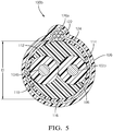
- Figs. 4 and 5 illustrate another non-limiting example of a wire cable 100b for transmitting electrical digital data signals.
- the wire cable 100b illustrated in Figs 4 and 5 is identical in construction to the wire cable 100a shown in Figs. 1 and 2 , with the exception that the first and second conductors 102b, 104b each comprise a solid wire conductor, such as a bare (non-plated) copper wire or silver plated copper wire having a cross section of about 0.321 square millimeters (mm 2 ), which is generally equivalent to 28 AWG solid wire.
- the first and second conductors 102b, 104b may be formed of a solid wire having a smaller gauge, such as 30 AWG or 32 AWG.
- the wire cable 100b may be characterized as having an impedance of 95 Ohms.
- Figs. 6 and 7 illustrate another non-limiting example of a wire cable 100c for transmitting electrical digital data signals.
- the wire cable 100c illustrated in Figs 6 and 7 is identical in construction to the wire cable 100b shown in Figs. 4 and 5 , with the exception that the drain wire 120b comprises a solid wire conductor, such as an unplated copper conductor, tin plated copper conductor, or silver plated copper conductor having a cross section of about 0.321 mm 2 , which is generally equivalent to 28 AWG solid wire.
- the drain wire 120b may be formed of solid wire having a smaller gauge, such as 30 AWG or 32 AWG.
- the wire cable 100c may be characterized as having an impedance of 95 Ohms.
- Fig. 8 illustrates yet another non-limiting example of a wire cable 100d for transmitting electrical digital data signals.
- the wire cable 100d illustrated in Figs 5 is similar to the construction to the wire cables 100a, 100b, 100c shown in Figs. 1-7 , however, wire cable 100d includes multiple pairs of first and second conductors 102b, 104b.
- the belting 112 also eliminates the need for a spacer to maintain separation of the wire pairs as seen in the prior art for wire cables having multiple wire pair conductors.
- the example illustrated in Fig. 8 includes solid wire conductors 102b, 104b, and 120b. However, alternative embodiments may include stranded wires 102a, 104a, and 120a.
- Fig. 9 illustrates the requirements for signal rise time (in picoseconds (ps)) and differential impedance (in Ohms ( ⁇ )) for the USB 3.0 and HDMI 1.3 performance specifications.
- Fig. 9 also illustrates the combined requirements for a wire cable capable of simultaneously meeting both USB 3.0 and HDMI 1.3 standards.
- the wire cable 100a - 100c is expected to meet the combined USB 3.0 and HDMI 1.3 signal rise time and differential impedance requirements shown in Fig. 9 .
- Fig. 10 illustrates the differential impedances that are expected for the wire cables 100a - 100c over a signal frequency range of 0 to 7500 MHz (7.5 GHz).
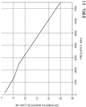
- Fig. 11 illustrates the insertion losses that are expected for wire cable 100a - 100c with a length of 7 m over the signal frequency range of 0 to 7500 MHz (7.5 GHz).
- the wire cable 100a - 100c having a length of up to 7 meters are expected to be capable of transmitting digital data at a speed of up to 5 Gigabits per second with an insertion loss of less than 20 dB.
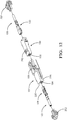
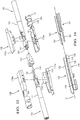
- the wire cable assembly also includes an electrical connector.
- the connector may be a receptacle connector 128 or a plug connector 130 configured to accept the receptacle connector 128.
- the receptacle connector 128 include two terminals, a first receptacle terminal 132 connected to a first inner conductor 102 and a second receptacle terminal 134 connected to a second inner conductor (not shown due to drawing perspective) of the wire cable 100.
- the first receptacle terminal 132 includes a first cantilever beam portion 136 that has a generally rectangular cross section and defines a convex first contact point 138 that depends from the first cantilever beam portion 136 near the free end of the first cantilever beam portion 136.
- the second receptacle terminal 134 also includes a similar second cantilever beam portion 140 having a generally rectangular cross section and defining a convex second contact point 142 depending from the second cantilever beam portion 140 near the free end of the second cantilever beam portion 140.
- the first and second receptacle terminals 132, 134 each comprise an attachment portion 144 that is configured to receive the end of an inner conductor of the wire cable 100 and provide a surface for attaching the first and second inner conductors 102, 104 to the first and second receptacle terminals 132, 134.
- the attachment portion 144 defines an L shape.
- the first and second receptacle terminals 132, 134 form a mirrored terminal pair that has bilateral symmetry about the longitudinal axis A and are substantially parallel to the longitudinal axis A and each other.
- the distance between the first cantilever beam portion 136 and the second cantilever beam portion 140 is 2.85 mm, center to center.
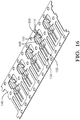
- the first and second receptacle terminals 132, 134 are formed from a sheet of conductive material by a stamping process that cuts out and bends the sheet to form the first and second receptacle terminals 132, 134.
- the stamping process also forms a carrier strip 146 to which the first and second receptacle terminals 132, 134 are attached.
- the first and second receptacle terminals 132, 134 are formed using a fine blanking process that provides a shear cut of at least 80% or greater through the stock thickness. This provides a smoother surface on the minor edges of the cantilever beam portions and the contact point that reduces connection abrasion between the receptacle connector 128 and the plug connector 130.
- the attachment portion 144 is then bent to the L shape in a subsequent forming operation.
- first and second receptacle terminals 132, 134 remain attached to the carrier strip 146 for an insert molding process that forms a receptacle terminal holder 148 that partially encases the first and second receptacle terminal 132, 134.
- the receptacle terminal holder 148 maintains the spatial relationship between the first and second receptacle terminals 132, 134 after they are separated from the carrier strip 146.
- the receptacle terminal holder 148 also defines a pair of wire guide channels 150 that help to maintain a consistent separation between the first and second inner conductors 102, 104 as they transition from the wire cable 100 to the attachment portions 144 of the first and second receptacle terminals 132, 134.
- the receptacle terminal holder 148 is formed of a dielectric material, such as a liquid crystal polymer. This material offers performance advantages over other engineering plastics, such as polyamide or polybutylene terephthalate, for molding, processing, and electrical dielectric characteristics.
- a portion of the carrier strip 146 is removed and a receptacle terminal cover 152 is then attached to the receptacle terminal holder 148.
- the receptacle terminal cover 152 is configured to protect the first and second receptacle terminals 132, 134 from bending while the receptacle connector 128 is being handled and when the plug connector 130 is being connected or disconnected with the receptacle connector 128.
- the receptacle terminal cover 152 defines a pair of grooves 154 that allow the first and second cantilever beam portions 136, 140 to flex when the plug connector 130 is connected to the receptacle connector 128.
- the receptacle terminal cover 152 may also be formed of same liquid crystal polymer material as the receptacle terminal holder 148, although other dielectric materials may alternatively be used.
- the receptacle terminal holder 148 defines an elongate slot 156 that mated to an elongate post 158 defined by the receptacle terminal holder 148.
- the receptacle terminal cover 152 is joined to the receptacle terminal holder 148 by ultrasonically welding the post 158 within the slot 156. Alternatively, other means of joining the receptacle terminal holder 148 to the receptacle terminal cover 152 may be employed.
- the remainder of the carrier strip 146 is removed from the first and second receptacle terminals 132, 134 prior to attaching the first and second inner conductors 102, 104 to the first and second receptacle terminals 132, 134.
- the first and second inner conductors 102, 104 are attached to the attachment portions 144 of the first and second receptacle terminals 132, 134 using an ultrasonic welding process. Sonically welding the conductors to the terminals allows better control of the mass of the joint between the conductor and the terminal than other joining processes such as soldering and therefore provides better control over the capacitance associated with the joint between the conductor and the terminal. It also avoids environmental issues caused by using solder.
- the plug connector 130 also includes two terminals, a first plug terminal 160 connected to a first inner conductor 102 and a second plug terminal 162 connected to a second inner conductor (not shown) of the wire cable 100.
- the first plug terminal 160 includes a first elongate planar portion 164 that has a generally rectangular cross section.
- the second plug terminal 162 also includes a similar second elongate planar portion 166.
- the planar portions of the plug terminals are configured to receive and contact the first and second contact points 138, 142 of the first and second receptacle terminals 132, 134.
- the free ends of the planar portions have a beveled shape to allow the mating first and second receptacle terminals 132, 134 to ride up and over free ends of the first and second planar portions 164, 166when the plug connector 130 and receptacle connector 128 are mated.
- the first and second plug terminals 160, 162 each comprise an attachment portion 144 similar to the attachment portions 144 of the first and second receptacle terminals 132, 134 that are configured to receive the ends of the first and second inner conductors 102, 104 and provide a surface for attaching the first and second inner conductors 102, 104 to the first and second plug terminals 160, 162.
- the attachment portion 144 defines an L shape.
- the first and second plug terminals 160, 162 form a mirrored terminal pair that has bilateral symmetry about the longitudinal axis A and are substantially parallel to the longitudinal axis A and each other.
- the distance between the first planar portion and the second planar portion is 2.85 mm, center to center.
- the inventors have observed through data obtained from computer simulation that the mirrored parallel receptacle terminals and plug terminals have a strong effect on the impedance and insertion loss of the wire cable assembly.
- the plug terminals are formed from a sheet of conductive material by a stamping process that cuts out and bends the sheet to form the plug terminals.
- the stamping process also forms a carrier strip 168 to which the plug terminals are attached.
- the attachment portion 144 is then bent to the L shape in a subsequent forming operation.
- the plug terminals remain attached to the carrier strip 168 for an insert molding process that forms a plug terminal holder 170 that partially encases the first and second plug terminals 160, 162.
- the plug terminal holder 170 maintains the spatial relationship between the first and second plug terminals 160, 162 after they are separated from the carrier strip 168.
- the plug terminal holder 170 similarly to the receptacle terminal holder 148, defines a pair of wire guide channels 150 that help to maintain a consistent separation between the first and second inner conductors 102, 104 as they transition from the wire cable 100 to the attachment portions 144 of the first and second receptacle terminals 132, 134.
- the plug terminal holder 170 is formed of a dielectric material, such as a liquid crystal polymer.
- the carrier strip 168 is removed from the plug terminals prior to attaching the first and second inner conductors 102, 104 to first and second plug terminals 160, 162.
- the first and second inner conductors 102, 104 of the wire cable 100 are attached to the attachment portions 144 of the first and second plug terminals 160, 162 using an ultrasonic welding process.
- the first and second plug terminals 160, 162 and the first and second receptacle terminals 132, 134 are oriented in the plug and receptacle connectors 128, 130 so that when the plug and receptacle connectors 128, 130 are mated, the major widths of the first and second receptacle terminals 132, 134 are substantially perpendicular to the major widths of the first and second plug terminals 160, 162.
- substantially perpendicular means that the major widths are ⁇ 15° of absolutely perpendicular.
- first and second plug terminals 160, 162 and the first and second receptacle terminals 132, 134 have strong effect on insertion loss. Also, when the plug and receptacle connectors 128, 130 are mated, the first and second receptacle terminals 132, 134 overlap the first and second plug terminals 160, 162.
- the plug and receptacle connectors 128, 130 are configured so that only the first and second contact points 138, 142 of the first and second receptacle terminals 132, 134 contacts the planar blade portion of the first and second plug terminals 160, 162 and the contact area defined between the first and second receptacle terminals 132, 134 and the first and second plug terminals 160, 162 is less than the area overlapped between the first and second receptacle terminals 132, 134 and the first and second plug terminals 160, 162. Therefore, the contact area, sometimes referred to as the wipe distance, is determined by the area of the first and second contact points 138, 142 and not by the overlap between the terminals.
- the receptacle and plug terminals provide the benefit of providing a consistent contact area as long as the first and second contact points 138, 142 of the first and second receptacle terminals 132, 134 are fully engaged with the first and second plug terminals 160, 162. Because the both the plug and receptacle terminals are a mirrored pair, a first contact area between the first receptacle terminal 132 and the first plug terminal 160 and a second contact area between the second receptacle terminal 134 and the second plug terminal 162 are substantially equal. As used herein, substantially equal means that the contact area difference between the first contact area and the second contact area is less than 0.1 mm 2 . The inventors have observed through data obtained from computer simulation that the contact area between the plug and receptacle terminals and the difference between the first contact are a and the second contact area have a strong impact on insertion loss of the wire cable assembly.
- the first and second plug terminals 160, 162 are not received within the first and second receptacle terminals 132, 134, therefore the first contact area is on the exterior of the first plug terminal 160 and the second contact area is on the exterior of the second plug terminal 162 when the plug connector 130 is mated to the receptacle connector 128.
- the first and second receptacle terminals 132, 134 and the first and second plug terminals 160, 162 may be formed from a sheet of copper-based material.
- the first and second cantilever beam portions 136, 140 and the first and second planar portions 164, 166 may be selectively plated using copper/nickel/silver based plating.
- the terminals may be plated to a 5 skin thickness.
- the first and second receptacle terminals 132, 134 and the first and second plug terminals 160, 162 are configured so that the receptacle connector 128 and plug connector 130 exhibit a low insertion normal force of about 0.4 Newton (45 grams). The low normal force provides the benefit of reducing abrasion of the plating during connection/disconnection cycles.
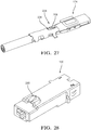
- the plug connector 130 includes a plug shield 172 that is attached to the outer shield 124 of the wire cable 100.
- the plug shield 172 is separated from and longitudinally surrounds the first and second plug terminals 160, 162 and plug terminal holder 170.
- the receptacle connector 128 also includes a receptacle shield 174 that is attached to the outer shield 124 of the wire cable 100 that is separated from and longitudinally surrounds the first and second receptacle terminals 132, 134, receptacle terminal holder 148 and receptacle terminal cover 152.
- the receptacle shield 174 and the plug shield 172 are configured to slidingly contact one another and when mated, provide electrical continuity between the outer shields of the attached wire cables 100 and electromagnetic shielding to the plug and receptacle connectors 128, 130.
- the plug shield 172 is made of two parts.
- the first plug shield 172A illustrated in Fig. 21 includes two pairs of crimping wings, conductor crimp wings 176 and insulator crimp wings 178, adjacent an attachment portion 180 configured to receive the wire cable 100.
- the conductor crimp wings 176 are bypass-type crimp wings that are offset and configured to surround the exposed outer shield 124 of the wire cable 100 when the conductor crimp wings 176 are crimped to the wire cable 110.
- the drain wire 120a is electrically coupled to the first plug shield 172A when the first plug shield 172A is crimped to the outer shield 124 because the drain wire 120a of the wire cable 100 is sandwiched between the outer shield 124 and the inner shield 116 of the wire cable 110. This provides the benefit of coupling the plug shield 172 to the drain wire 120 without having to orient the drain wire 120 in relation to the shield before crimping.
- the attachment portion 180 and the interior of the conductor crimp wings 176 may define a plurality of rhomboid indentations configured to improve electrical connectivity between the first plug shield 172A and the outer shield 124 of the wire cable 100.
- rhomboid indentations are described in U.S. Patent No. 8,485,853 , the entire disclosure of which is hereby incorporated by reference.
- the insulation crimp wings are also bypass type wings that are offset and configured to surround the jacket 126 of the wire cable 100 when the plug shield 172 is crimped to the wire cable 110.
- the each of the insulation crimp wings further include a prong 182 having a pointed end that is configured to penetrate at least the outer insulator of the wire cable 100.
- the prongs 182 inhibit the plug shield 172 from being separated from the wire cable 100 when a force is applied between the plug shield 172 and the wire cable 100.
- the prongs 182 also inhibit the plug shield 172 from rotating about the longitudinal axis A of the wire cable 100.
- the prongs 182 may also penetrate the outer shield 124, inner shield 116, or belting 112 of the wire cable 100 but should not penetrate the first and second insulators 108, 110. While the illustrated example includes two prongs 182, alternative embodiments of the invention may be envisioned using only a single prong 182 define by the first plug shield 172A.
- the first plug shield 172A defines an embossed portion 184 that is proximate to the connection between the attachment portions 144 of the plug terminals and the first and second inner conductors 102, 104.
- the embossed portion 184 increases the distance between the attachment portions 144 and the first plug shield 172A, thus decreasing the capacitive coupling between them.
- the first plug shield 172A further defines a plurality of protrusions 218 or bumps 186 that are configured to interface with a corresponding plurality of holes 188 defined in the second plug shield 172B as shown in Fig. 22 .
- the bumps 186 are configured to snap into the holes 188, thus mechanically securing and electrically connecting the second plug shield 172B to the first plug shield 172A.
- the receptacle shield 174 is similarly made of two parts.
- the first receptacle shield 174A illustrated in Fig. 23 , includes two pairs of crimping wings, conductor crimp wings 176 and insulator crimp wings 178, adjacent an attachment portion 180 configured to receive the wire cable 110.
- the conductor crimp wings 176 are bypass-type crimp wings that are offset and configured to surround the exposed outer shield 124 of the wire cable 100 when the conductor crimp wings 176 are crimped to the wire cable 100.
- the attachment portion 144 and the interior of the conductor crimp wings 176 may define a plurality of rhomboid indentations configured to improve electrical connectivity between the first plug shield 172A and the outer shield 124 of the wire cable 100.
- the insulation crimp wings are also bypass type wings that are offset and configured to surround the jacket 126 of the wire cable 100 when the plug shield 172 is crimped to the wire cable 100.
- the insulation crimp wings further include a prong 182 having a pointed end that is configured to penetrate at least the outer insulator of the wire cable 100.
- the prongs 182 may also penetrate the outer shield 124, inner shield 116, or belting of the wire cable 100. While the illustrated example includes two prongs 182, alternative embodiments of the invention may be envisioned using only a single prong 182.
- the first receptacle shield 174A defines a plurality of protrusions 218 or bumps 186 that are configured to interface with a corresponding plurality of holes 188 defined in the second receptacle shield 174B securing the second receptacle shield 174 to the first receptacle shield 174A.
- the first receptacle shield 174A may not define an embossed portion proximate the connection between the attachment portions 144 of the first and second receptacle terminals 132, 134 and the first and second inner conductors 102, 104 because the distance between the connection and the receptacle shield 174 is larger to accommodate insertion of the plug shield 172 within the receptacle shield 174.
- the exterior of the plug shield 172 of the illustrated example is configured to slideably engage the interior of the receptacle shield 174
- alternative embodiments may be envisioned wherein the exterior of the receptacle shield 174 slidably engages the interior of the plug shield 172.
- the receptacle shield 174 and the plug shield 172 may be formed from a sheet of copper-based material.
- the receptacle shield 174 and the plug shield 172 may be plated using copper/nickel/silver or tin based plating.
- the first and second receptacle shield 174A, 174B and the first and second plug shield 172A, 172B may be formed by stamping processes well known to those skilled in the art.
- plug connector and receptacle connector While the examples of the plug connector and receptacle connector illustrated herein are connected to a wire cable, other embodiments of the plug connector and receptacle connector may be envisioned that are connected to conductive traces on a circuit board.
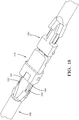
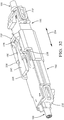
- the wire cable assembly 100 may further include a plug connector body 190 and a receptacle connector body 192 as illustrated in Fig. 12 .
- the plug connector body 190 and the receptacle connector body 192 are formed of a dielectric material, such as a polyester material.
- the receptacle connector body 192 defines a cavity 194 that receives the receptacle connector 128.
- the receptacle connector body 192 also defines a shroud configured to accept the plug connector body 190.
- the receptacle connector body 192 further defines a low profile latching mechanism with a locking arm 196 configured to secure the receptacle connector body 192 to the plug connector body 190 when the plug and receptacle connector bodies 190, 192 are fully mated.
- the plug connector body 190 similarly defines a cavity 198 that receives the plug connector 130.
- the plug connector body 190 defines a lock tab 200 that is engaged by the locking arm 196 to secure the receptacle connector body 192 to the plug connector body 190 when the plug and receptacle connector bodies 190, 192 are fully mated.
- the wire cable assembly 100 also includes connector position assurance devices 202 that hold the receptacle connector 128 and the plug connector 130 within their respective connector body cavities 194, 198.
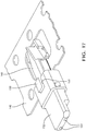
- the first plug shield 172A defines a triangular lock tang 204 that protrudes from the first plug shield 172A and is configured to secure the plug connector 130 within the cavity 198 of the plug connector body 190.
- the lock tang 204 includes a fixed edge (not shown) that is attached to the first plug shield 172A and is substantially parallel with a longitudinal axis A of the plug shield 172, a leading edge 206 that is unattached to the first plug shield 172A and defines an acute angle relative to the longitudinal axis A, and a trailing edge 208 that is also unattached to the first plug shield 172A and is substantially perpendicular to the longitudinal axis A.
- the cavity 198 of the plug connector body 190 includes a narrow portion 210 and a wide portion 212.
- the leading edge 206 of the lock tang 204 contacts a top wall 214 of the narrow portion 210 and compresses the lock tang 204, allowing the plug connector 130 to pass through the narrow portion 210 of the cavity 198.
- the lock tang 204 enters the wide portion 212 of the cavity 198, the lock tang 204 returns to its uncompressed shape.
- the trailing edge 208 of the lock tang 204 then contacts a back wall 216 of the wide portion 212 of the cavity 198, inhibiting the plug connector 130 from passing back through the narrow portion 210 of the plug connector body cavity 198.
- the lock tang 204 may be compressed so that the plug connector 130 may be removed from the cavity 198 by inserting a pick tool in the front of the wide portion 212 of the cavity 198.
- the receptacle shield 174 defines a similar lock tang 204 configured to secure the receptacle connector 128 within the cavity 194 of the receptacle connector body 192.
- the cavity 194 of the receptacle connector body 192 includes similar wide and narrow potions that have similar top walls and back walls.
- the lock tangs 204 may be formed during the stamping process of forming the first plug shield 172A and the first receptacle shield 174A.
- the receptacle shield 174 also includes a pair of protrusions 218 configured interface with a pair of grooves 220 defined in the side walls of the receptacle connector body cavity 194 to align and orient the receptacle connector 128 within the cavity 194 of the receptacle connector body 192.
- the plug shield 172 similarly defines a pair of protrusions 218 configured interface with a pair of grooves (not shown due to drawing perspective) defined in the side walls of the plug connector body cavity 198 to align and orient the plug connector 130 within the cavity 198 of the plug connector body 190.
- receptacle and plug connector bodies 190, 192 illustrated in Fig. 12 include only a single cavity, other embodiments of the connector bodies may be envisioned that include a plurality of cavities so that the connector bodies include multiple plug and receptacle connectors 128, 130 or alternatively contain other connector types in addition to the plug or receptacle connectors 128, 130.
- the receptacle connector body 192 defines the lock tab 200 that extends outwardly from the receptacle connector body 192.
- the plug connector body 190 includes a longitudinally extending lock arm 196.
- a free end 222 of the lock arm 196 defines an inwardly extending lock nib 224 that is configured to engage the lock tab 200 of the receptacle connector body 192.
- the free end 222 of the lock arm 196 also defines an outwardly extending stop 226.
- the lock arm 196 is integrally connected to the socket connector body by a resilient U-shaped strap 228 that is configured to impose a hold-down force 230 on the free end 222 of the lock arm 196 when the lock arm 196 is pivoted from a state of rest.
- the plug connector body 190 further includes a transverse hold down beam 232 integrally that is connected to the plug connector body 190 between fixed ends and configured to engage the stop 226 when a longitudinal separating force 234 applied between the receptacle connector body 192 and the plug connector body 190 exceeds a first threshold.
- a longitudinal separating force 234 applied between the receptacle connector body 192 and the plug connector body 190 exceeds a first threshold when the separating force 234 is applied, the front portion 236 of the U-shaped strap 228 is displaced by the separating force 234 until the stop 226 on the free end 222 of the lock arm 196 contacts the hold down beam 232.
- This contact between the stop 226 and the hold down beam 232 increases the hold-down force 230 on the lock nib 224, thereby maintaining engagement of the lock nib 224 with the lock tab 200, this inhibiting separation of the plug connector body 190 from the receptacle connector body 192.
- the plug connector body 190 further comprises a shoulder 238 that is generally coplanar with the U-shaped strap 228 and is configured to engage the U-shaped strap 228.
- a shoulder 238 that is generally coplanar with the U-shaped strap 228 and is configured to engage the U-shaped strap 228.
- the lock arm 196 also includes a depressible handle 240 that is disposed rearward of the U-shaped strap 228.
- the lock nib 224 is moveable outwardly away from the lock tab 200 by depressing the handle to enable disengagement of the lock nib 224 with the lock tab 200.
- the lock arm 196 further includes an inwardly extending fulcrum 242 disposed between the lock nib 224 and the depressible handle 240.
- a wire cable assembly 100a - 100c is provided.
- the wire cable 100a - 100c is capable of transmitting digital data signals with data rates of 5 Gb/s or higher.
- the wire cable 100a - 100c is capable of transmitting signals at this rate over a single pair of conductors rather than multiple twisted pairs as used in other high speed cables capable of supporting similar data transfer rates, such as Category 7 cable.
- Using a single pair as in wire cable 100a - 100c provides the advantage of eliminating the possibility for cross talk that occurs between twisted pairs in other wire cables 100a having multiple twisted pairs.
- the single wire pair in wire cable 100a - 100c also reduces the mass of the wire cable 100a - 100c; an important factor in weight sensitive applications such as automotive and aerospace.
- the belting 112 between the first and second conductors 102a, 104a, 102b, 104b and the inner shield 116 helps to maintain a consistent radial distance between the first and second conductors 102a, 104a, 102b, 104b and the inner shield 116 especially when the cable is bent as is required in routing the wire cable 100a - 100c within an automotive wiring harness assembly. Maintaining the consistent radial distance between the first and second conductors 102a, 104a, 102b, 104b and the inner shield 116 provides for consistent cable impedance and more reliable data transfer rates.
- the belting 112 and the bonding of the first and second insulators 108, 110 helps to maintain the twist angle ⁇ between the first and second conductors 102a, 104a, 102b, 104b in the wire pair, again, especially when the cable is bent by being routed through the vehicle at angles that would normally induce wire separation between the first and second conductor 102, 104.
- This also provides consistent cable impedance.
- the receptacle connectors 128 and plug connectors 130 cooperate with the wire cable to provide consistent cable impedance.
Claims (12)
- Elektrisches Verbindungssystem, das aufweist:einen Steckverbinder (130) mit einem ersten Steckanschluss (160), der einen planaren ersten Verbindungsteil (164) mit einem im Allgemeinen rechteckigen Querschnitt und einen ersten Befestigungsteil (144) umfasst, der konfiguriert ist zur Befestigung an einem ersten elektrischen Leiter (102), und einem zweiten Steckanschluss (162), der einen planaren zweiten Verbindungsteil (166) mit einem im Allgemeinen rechteckigen Querschnitt und einen zweiten Befestigungsteil (144) umfasst, der konfiguriert ist zur Befestigung an einem zweiten elektrischen Leiter (104), wobei der erste und der zweite Steckanschluss (160, 162) ein erstes gespiegeltes Anschlusspaar mit bilateraler Symmetrie um eine Längsachse (A) bilden; und einen Buchsenverbinder (128), der konfiguriert ist zum Zusammenfügen mit dem Steckverbinder (130) mit einem ersten Buchsenanschluss (132), der einen dritten Befestigungsteil (144) umfasst, der konfiguriert ist zur Befestigung an einem dritten elektrischen Leiter (102), und einen ersten freitragenden Armteil (136) mit einem im Allgemeinen rechteckigen Querschnitt, der einen konvexen ersten Kontaktpunkt (138) abhängig von dem ersten freitragenden Armteil (136) definiert, wobei der erste Kontaktpunkt (138) konfiguriert ist zum Kontaktieren des ersten Verbindungsteils (164) des ersten Steckanschlusses (160), und mit einem zweiten Buchsenanschluss (134), der einen vierten Befestigungsteil (144) umfasst, der konfiguriert ist zur Befestigung an einem vierten elektrischen Leiter (104), und einen zweiten freitragenden Armteil (140) mit einem im Allgemeinen rechteckigen Querschnitt, der einen konvexen zweiten Kontaktpunkt (142) abhängig von dem zweiten freitragenden Armteil (140) definiert, wobei der zweite Kontaktpunkt (142) konfiguriert ist zum Kontaktieren des zweiten Verbindungsteils (166) des zweiten Steckanschlusses (162), wobei der erste und der zweite Buchsenanschluss (132, 134) ein zweites gespiegeltes Anschlusspaar mit bilateraler Symmetrie um die Längsachse (A) bilden, und wobei, wenn der Steckverbinder (130) mit dem Buchsenverbinder (128) verbunden ist, die Hauptbreite des ersten Verbindungsteils (164) im Wesentlichen senkrecht zu der Hauptbreite des ersten freitragenden Armteils (136) ist und der zweite Verbindungsteil (166) im Wesentlichen senkrecht zu der Hauptbreite des zweiten freitragenden Armteils (140) ist, dadurch gekennzeichnet, dass die Befestigungsteile (144) der Steckanschlüsse (160, 162) und die Befestigungsteile (144) der Buchsenanschlüsse (132, 134) eine L-Form haben.
- Das elektrische Verbindungssystem gemäß Anspruch 1, wobei der erste und der zweite Verbindungsteil (164, 166) im Wesentlichen parallel zueinander sind und wobei der erste und der zweite freitragende Armteil (136, 140) im Wesentlichen parallel zueinander sind.
- Das elektrische Verbindungssystem gemäß Anspruch 1 oder 2, wobei ein erster Kontaktbereich, der zwischen dem ersten Verbindungsteil (164) und dem ersten Kontaktpunkt (138) definiert ist, im Wesentlichen gleich zu einem zweiten Kontaktbereich ist, der zwischen dem zweiten Verbindungsteil (166) und dem zweiten Kontaktpunkt (142) definiert ist, wenn der Steckverbinder (130) mit dem Buchsenverbinder (128) zusammengefügt ist.
- Das elektrische Verbindungssystem gemäß Anspruch 3, wobei der erste Kontaktbereich außerhalb des ersten Steckanschlusses (160) ist und der zweite Kontaktbereich außerhalb des zweiten Steckanschlusses (162) ist, wenn der Steckverbinder (130) mit dem Buchsenverbinder (128) zusammengefügt ist.
- Das elektrische Verbindungssystem gemäß Anspruch 2 oder 3, wobei der erste Kontaktbereich konfiguriert ist, kleiner als ein erster Überlappungsbereich zu sein, der durch einen ersten Überlappungsbereich zwischen dem ersten Buchsenanschluss (132) und dem ersten Steckanschluss (160) definiert ist, und der zweite Kontaktbereich konfiguriert ist, kleiner zu sein als ein zweiter Überlappungsbereich, der durch einen zweiten Überlappungsbereich zwischen dem zweiten Buchsenanschluss (134) und dem zweiten Steckanschluss (162) definiert ist, wenn der Steckverbinder (130) mit dem Buchsenverbinder (128) zusammengefügt ist.
- Das elektrische Verbindungssystem gemäß einem der vorhergehenden Ansprüche, wobei der erste und der zweite Steckanschluss (160, 162) teilweise in einem Steckanschlusshalter (170) eingeschlossen sind, der aus einem dielektrischen Material gebildet ist und konfiguriert ist zum Beibehalten einer lateralen Trennung des ersten und des zweiten Steckanschlusses (160, 162).
- Das elektrische Verbindungssystem gemäß einem der vorhergehenden Ansprüche, wobei der erste und der zweite Buchsenanschluss (132, 134) teilweise in einem Buchsenanschlusshalter (148) eingeschlossen sind, der aus einem dielektrischen Material gebildet ist und konfiguriert zum Beibehalten einer lateralen Trennung des ersten und des zweiten Buchsenanschlusses (132, 134).
- Das elektrische Verbindungssystem gemäß Anspruch 7, wobei der Buchsenanschlusshalter (148) ein Paar von Kanälen angrenzend an den ersten und den zweiten Buchsenanschluss (132, 134) definiert, die konfiguriert sind zum Ermöglichen einer vertikalen Ablenkung des ersten und des zweiten Buchsenanschlusses (132, 134).
- Das elektrische Verbindungssystem gemäß einem der vorhergehenden Ansprüche, wobei der erste und der zweite elektrische Leiter (102, 104) aus der Gruppe ausgewählt ist, die aus Drahtleitern und leitenden Leiterplattenbahnen besteht.
- Das elektrische Verbindungssystem gemäß einem der vorhergehenden Ansprüche, wobei der dritte und der vierte elektrische Leiter (102, 104) aus der Gruppe ausgewählt ist, die aus Drahtleitern und leitenden Leiterplattenbahnen besteht.
- Das elektrische Verbindungssystem gemäß einem der vorhergehenden Ansprüche, das weiter aufweist:eine Steckerabschirmung (172), die von dem Steckverbinder (130) elektrisch isoliert ist und konfiguriert ist, an einem ersten Abschirmungsleiter (124) angebracht zu sein und den Steckverbinder (130) in Längsrichtung zu umgeben; undeine Buchsenabschirmung (174), die von dem Buchsenverbinder (128) elektrisch isoliert ist und konfiguriert ist, an einem zweiten Abschirmleiter (124) angebracht zu sein und den Buchsenverbinder (128) in Längsrichtung zu umgeben.
- Das elektrische Verbindungssystem gemäß Anspruch 11, wobei die Buchsenabschirmung (174) konfiguriert ist, gleitend in das Innere der Steckerabschirmung (172) einzugreifen, und wobei die Buchsenabschirmung (174) eine Prägung (184) nahe einer Position einer Verbindung zwischen dem dritten und dem vierten elektrischen Leiter (102, 104) und dem dritten und dem vierten Befestigungsteil (144) definiert, wobei die Prägung (184) einen Abstand zwischen dem dritten und vierten Befestigungsteil (144) und der Buchsenabschirmung (174) vergrößert, wodurch eine kapazitive Kopplung zwischen dem dritten und vierten elektrischen Leiter (102, 104) und der Buchsenabschirmung (174) verringert wird.
Applications Claiming Priority (1)
| Application Number | Priority Date | Filing Date | Title |
|---|---|---|---|
| US14/101,482 US9142907B2 (en) | 2013-12-10 | 2013-12-10 | Electrical connection system |
Publications (2)
| Publication Number | Publication Date |
|---|---|
| EP2884592A1 EP2884592A1 (de) | 2015-06-17 |
| EP2884592B1 true EP2884592B1 (de) | 2018-04-18 |
Family
ID=52002851
Family Applications (1)
| Application Number | Title | Priority Date | Filing Date |
|---|---|---|---|
| EP14196316.5A Active EP2884592B1 (de) | 2013-12-10 | 2014-12-04 | Elektrisches Verbindungssystem |
Country Status (5)
| Country | Link |
|---|---|
| US (1) | US9142907B2 (de) |
| EP (1) | EP2884592B1 (de) |
| JP (2) | JP2015130327A (de) |
| KR (1) | KR101611101B1 (de) |
| CN (1) | CN104701655B (de) |
Families Citing this family (13)
| Publication number | Priority date | Publication date | Assignee | Title |
|---|---|---|---|---|
| WO2015115093A1 (ja) * | 2014-01-31 | 2015-08-06 | パナソニックIpマネジメント株式会社 | コネクタおよびコネクタ装置 |
| JP2017017886A (ja) * | 2015-07-02 | 2017-01-19 | 住友電気工業株式会社 | 多芯ケーブル |
| JP6729273B2 (ja) * | 2016-10-12 | 2020-07-22 | 株式会社オートネットワーク技術研究所 | コネクタ構造 |
| JP6961409B2 (ja) * | 2017-07-12 | 2021-11-05 | ヒロセ電機株式会社 | かしめ構造を有するケーブルコネクタ |
| JP2019106355A (ja) * | 2017-11-03 | 2019-06-27 | アプティブ・テクノロジーズ・リミテッド | シールドされたワイヤケーブル用の電気接続システム |
| JP6752260B2 (ja) * | 2017-11-06 | 2020-09-09 | アプティブ・テクノロジーズ・リミテッド | シールドされたワイヤケーブル用の電気接続システム |
| EP3528343A1 (de) * | 2018-02-16 | 2019-08-21 | Aptiv Technologies Limited | Elektrisches abschirmungselement für einen netzwerkverbinder |
| EP3561967B1 (de) * | 2018-04-25 | 2024-03-20 | Aptiv Technologies Limited | Elektrisches abschirmungselement für einen netzwerkverbinder |
| JP7172750B2 (ja) * | 2019-03-07 | 2022-11-16 | 株式会社オートネットワーク技術研究所 | シールド構造、及びワイヤーハーネス |
| JP7371505B2 (ja) * | 2020-01-20 | 2023-10-31 | 住友電装株式会社 | ワイヤハーネス |
| US11696426B2 (en) * | 2020-02-26 | 2023-07-04 | Marvell Asia Pte Ltd | Automotive network communication devices and cabling with electromagnetic shielding |
| CN115051178A (zh) * | 2021-03-08 | 2022-09-13 | 贝尔威勒电子(昆山)有限公司 | 电流传输组件与电流传输系统 |
| CN114142256A (zh) * | 2021-11-02 | 2022-03-04 | 北京卫星制造厂有限公司 | 一种射频电缆连接器 |
Citations (1)
| Publication number | Priority date | Publication date | Assignee | Title |
|---|---|---|---|---|
| JP2013182753A (ja) * | 2012-03-01 | 2013-09-12 | Hosiden Corp | マイクロusbプラグ |
Family Cites Families (15)
| Publication number | Priority date | Publication date | Assignee | Title |
|---|---|---|---|---|
| JP2988237B2 (ja) * | 1994-01-31 | 1999-12-13 | 住友電装株式会社 | 簡易防水コネクタ |
| US6039610A (en) | 1998-04-08 | 2000-03-21 | The Whitaker Corporation | Multiple circuit fork contact connector |
| CN1100369C (zh) * | 1998-04-28 | 2003-01-29 | 住友电装株式会社 | 阳插接件和阴插接件对及配合插接件套件 |
| JP2000260521A (ja) * | 1999-03-09 | 2000-09-22 | Yazaki Corp | コネクタ |
| US6508678B1 (en) | 2000-08-31 | 2003-01-21 | Advanced Connecteck Inc. | Electrical connector assembly |
| JP4093444B2 (ja) * | 2000-09-05 | 2008-06-04 | ヒロセ電機株式会社 | シールドケース付電気コネクタ |
| JP3921051B2 (ja) * | 2001-01-15 | 2007-05-30 | 矢崎総業株式会社 | コネクタ |
| JP2002367718A (ja) * | 2001-06-07 | 2002-12-20 | Auto Network Gijutsu Kenkyusho:Kk | コネクタ |
| JP2005317260A (ja) * | 2004-04-27 | 2005-11-10 | Tyco Electronics Amp Kk | 同軸コネクタ |
| US7374460B1 (en) * | 2007-04-17 | 2008-05-20 | Traxxas Lp | Electrical connector assembly |
| JP4897626B2 (ja) * | 2007-09-18 | 2012-03-14 | ホシデン株式会社 | コネクタ |
| US7727020B2 (en) * | 2008-09-05 | 2010-06-01 | Delphi Technologies, Inc. | Cable connector |
| US7909646B2 (en) * | 2009-08-10 | 2011-03-22 | 3M Innovative Properties Company | Electrical carrier assembly and system of electrical carrier assemblies |
| US7927123B2 (en) | 2009-09-17 | 2011-04-19 | Cheng Uei Precision Industry Co., Ltd. | Battery connector |
| US8485853B2 (en) | 2011-11-03 | 2013-07-16 | Delphi Technologies, Inc. | Electrical contact having knurl pattern with recessed rhombic elements that each have an axial minor distance |
-
2013
- 2013-12-10 US US14/101,482 patent/US9142907B2/en active Active
-
2014
- 2014-11-21 JP JP2014236124A patent/JP2015130327A/ja not_active Withdrawn
- 2014-12-04 EP EP14196316.5A patent/EP2884592B1/de active Active
- 2014-12-05 KR KR1020140173948A patent/KR101611101B1/ko active IP Right Grant
- 2014-12-09 CN CN201410748457.0A patent/CN104701655B/zh active Active
-
2016
- 2016-12-27 JP JP2016253137A patent/JP2017103236A/ja active Pending
Patent Citations (1)
| Publication number | Priority date | Publication date | Assignee | Title |
|---|---|---|---|---|
| JP2013182753A (ja) * | 2012-03-01 | 2013-09-12 | Hosiden Corp | マイクロusbプラグ |
Also Published As
| Publication number | Publication date |
|---|---|
| EP2884592A1 (de) | 2015-06-17 |
| CN104701655B (zh) | 2017-06-23 |
| KR20150067733A (ko) | 2015-06-18 |
| KR101611101B1 (ko) | 2016-04-08 |
| JP2017103236A (ja) | 2017-06-08 |
| US9142907B2 (en) | 2015-09-22 |
| US20150162692A1 (en) | 2015-06-11 |
| CN104701655A (zh) | 2015-06-10 |
| JP2015130327A (ja) | 2015-07-16 |
Similar Documents
| Publication | Publication Date | Title |
|---|---|---|
| EP2779176B1 (de) | Abgeschirmte Kabelanordnung | |
| US20170110222A1 (en) | Shielded cable assembly | |
| EP2884592B1 (de) | Elektrisches Verbindungssystem | |
| US11336058B2 (en) | Shielded cable assembly | |
| EP2884588B1 (de) | Elektrische Anschlussklemme | |
| EP3091614A1 (de) | Electrical shield connector | |
| EP3096331B1 (de) | Abgeschirmte kabelanordnung | |
| CN109755816B (zh) | 用于屏蔽线缆的电连接系统 | |
| EP3098905A1 (de) | Elektrischer abschirmungsstecker | |
| EP2884596B1 (de) | Verbinderarretiermechanismus mit niedrigem Profil | |
| EP3480899B1 (de) | Stromanschlusssystem für abgeschirmtes drahtkabel | |
| US9698501B2 (en) | Electrical shield connector | |
| US10109958B2 (en) | Electrical connection system for shielded wire cable |
Legal Events
| Date | Code | Title | Description |
|---|---|---|---|
| PUAI | Public reference made under article 153(3) epc to a published international application that has entered the european phase |
Free format text: ORIGINAL CODE: 0009012 |
|
| 17P | Request for examination filed |
Effective date: 20141204 |
|
| AK | Designated contracting states |
Kind code of ref document: A1 Designated state(s): AL AT BE BG CH CY CZ DE DK EE ES FI FR GB GR HR HU IE IS IT LI LT LU LV MC MK MT NL NO PL PT RO RS SE SI SK SM TR |
|
| AX | Request for extension of the european patent |
Extension state: BA ME |
|
| R17P | Request for examination filed (corrected) |
Effective date: 20151217 |
|
| RBV | Designated contracting states (corrected) |
Designated state(s): AL AT BE BG CH CY CZ DE DK EE ES FI FR GB GR HR HU IE IS IT LI LT LU LV MC MK MT NL NO PL PT RO RS SE SI SK SM TR |
|
| 17Q | First examination report despatched |
Effective date: 20161219 |
|
| RIC1 | Information provided on ipc code assigned before grant |
Ipc: H01R 24/28 20110101ALI20170724BHEP Ipc: H01R 13/6582 20110101ALN20170724BHEP Ipc: H01R 13/627 20060101ALN20170724BHEP Ipc: H01R 9/05 20060101ALN20170724BHEP Ipc: H01R 9/053 20060101ALN20170724BHEP Ipc: H01R 4/18 20060101ALN20170724BHEP Ipc: H01R 13/432 20060101ALN20170724BHEP Ipc: H01R 13/26 20060101AFI20170724BHEP Ipc: H01R 103/00 20060101ALN20170724BHEP Ipc: H01R 13/50 20060101ALN20170724BHEP |
|
| GRAP | Despatch of communication of intention to grant a patent |
Free format text: ORIGINAL CODE: EPIDOSNIGR1 |
|
| GRAJ | Information related to disapproval of communication of intention to grant by the applicant or resumption of examination proceedings by the epo deleted |
Free format text: ORIGINAL CODE: EPIDOSDIGR1 |
|
| RIC1 | Information provided on ipc code assigned before grant |
Ipc: H01R 13/26 20060101AFI20171019BHEP Ipc: H01R 4/18 20060101ALN20171019BHEP Ipc: H01R 13/432 20060101ALN20171019BHEP Ipc: H01R 9/05 20060101ALN20171019BHEP Ipc: H01R 13/50 20060101ALN20171019BHEP Ipc: H01R 13/6582 20110101ALN20171019BHEP Ipc: H01R 13/627 20060101ALN20171019BHEP Ipc: H01R 9/053 20060101ALN20171019BHEP Ipc: H01R 103/00 20060101ALN20171019BHEP Ipc: H01R 24/28 20110101ALI20171019BHEP |
|
| GRAP | Despatch of communication of intention to grant a patent |
Free format text: ORIGINAL CODE: EPIDOSNIGR1 |
|
| INTG | Intention to grant announced |
Effective date: 20171120 |
|
| INTG | Intention to grant announced |
Effective date: 20171128 |
|
| GRAS | Grant fee paid |
Free format text: ORIGINAL CODE: EPIDOSNIGR3 |
|
| GRAA | (expected) grant |
Free format text: ORIGINAL CODE: 0009210 |
|
| AK | Designated contracting states |
Kind code of ref document: B1 Designated state(s): AL AT BE BG CH CY CZ DE DK EE ES FI FR GB GR HR HU IE IS IT LI LT LU LV MC MK MT NL NO PL PT RO RS SE SI SK SM TR |
|
| REG | Reference to a national code |
Ref country code: GB Ref legal event code: FG4D |
|
| REG | Reference to a national code |
Ref country code: CH Ref legal event code: EP |
|
| REG | Reference to a national code |
Ref country code: AT Ref legal event code: REF Ref document number: 991414 Country of ref document: AT Kind code of ref document: T Effective date: 20180515 |
|
| REG | Reference to a national code |
Ref country code: IE Ref legal event code: FG4D |
|
| REG | Reference to a national code |
Ref country code: DE Ref legal event code: R096 Ref document number: 602014024032 Country of ref document: DE |
|
| REG | Reference to a national code |
Ref country code: NL Ref legal event code: MP Effective date: 20180418 |
|
| REG | Reference to a national code |
Ref country code: LT Ref legal event code: MG4D |
|
| PG25 | Lapsed in a contracting state [announced via postgrant information from national office to epo] |
Ref country code: NL Free format text: LAPSE BECAUSE OF FAILURE TO SUBMIT A TRANSLATION OF THE DESCRIPTION OR TO PAY THE FEE WITHIN THE PRESCRIBED TIME-LIMIT Effective date: 20180418 |
|
| PG25 | Lapsed in a contracting state [announced via postgrant information from national office to epo] |
Ref country code: LT Free format text: LAPSE BECAUSE OF FAILURE TO SUBMIT A TRANSLATION OF THE DESCRIPTION OR TO PAY THE FEE WITHIN THE PRESCRIBED TIME-LIMIT Effective date: 20180418 Ref country code: PL Free format text: LAPSE BECAUSE OF FAILURE TO SUBMIT A TRANSLATION OF THE DESCRIPTION OR TO PAY THE FEE WITHIN THE PRESCRIBED TIME-LIMIT Effective date: 20180418 Ref country code: ES Free format text: LAPSE BECAUSE OF FAILURE TO SUBMIT A TRANSLATION OF THE DESCRIPTION OR TO PAY THE FEE WITHIN THE PRESCRIBED TIME-LIMIT Effective date: 20180418 Ref country code: SE Free format text: LAPSE BECAUSE OF FAILURE TO SUBMIT A TRANSLATION OF THE DESCRIPTION OR TO PAY THE FEE WITHIN THE PRESCRIBED TIME-LIMIT Effective date: 20180418 Ref country code: BG Free format text: LAPSE BECAUSE OF FAILURE TO SUBMIT A TRANSLATION OF THE DESCRIPTION OR TO PAY THE FEE WITHIN THE PRESCRIBED TIME-LIMIT Effective date: 20180718 Ref country code: NO Free format text: LAPSE BECAUSE OF FAILURE TO SUBMIT A TRANSLATION OF THE DESCRIPTION OR TO PAY THE FEE WITHIN THE PRESCRIBED TIME-LIMIT Effective date: 20180718 Ref country code: FI Free format text: LAPSE BECAUSE OF FAILURE TO SUBMIT A TRANSLATION OF THE DESCRIPTION OR TO PAY THE FEE WITHIN THE PRESCRIBED TIME-LIMIT Effective date: 20180418 Ref country code: AL Free format text: LAPSE BECAUSE OF FAILURE TO SUBMIT A TRANSLATION OF THE DESCRIPTION OR TO PAY THE FEE WITHIN THE PRESCRIBED TIME-LIMIT Effective date: 20180418 |
|
| PG25 | Lapsed in a contracting state [announced via postgrant information from national office to epo] |
Ref country code: RS Free format text: LAPSE BECAUSE OF FAILURE TO SUBMIT A TRANSLATION OF THE DESCRIPTION OR TO PAY THE FEE WITHIN THE PRESCRIBED TIME-LIMIT Effective date: 20180418 Ref country code: LV Free format text: LAPSE BECAUSE OF FAILURE TO SUBMIT A TRANSLATION OF THE DESCRIPTION OR TO PAY THE FEE WITHIN THE PRESCRIBED TIME-LIMIT Effective date: 20180418 Ref country code: HR Free format text: LAPSE BECAUSE OF FAILURE TO SUBMIT A TRANSLATION OF THE DESCRIPTION OR TO PAY THE FEE WITHIN THE PRESCRIBED TIME-LIMIT Effective date: 20180418 Ref country code: GR Free format text: LAPSE BECAUSE OF FAILURE TO SUBMIT A TRANSLATION OF THE DESCRIPTION OR TO PAY THE FEE WITHIN THE PRESCRIBED TIME-LIMIT Effective date: 20180719 |
|
| REG | Reference to a national code |
Ref country code: DE Ref legal event code: R081 Ref document number: 602014024032 Country of ref document: DE Owner name: APTIV TECHNOLOGIES LIMITED, BB Free format text: FORMER OWNER: DELPHI TECHNOLOGIES, INC., TROY, MICH., US |
|
| REG | Reference to a national code |
Ref country code: AT Ref legal event code: MK05 Ref document number: 991414 Country of ref document: AT Kind code of ref document: T Effective date: 20180418 |
|
| PG25 | Lapsed in a contracting state [announced via postgrant information from national office to epo] |
Ref country code: PT Free format text: LAPSE BECAUSE OF FAILURE TO SUBMIT A TRANSLATION OF THE DESCRIPTION OR TO PAY THE FEE WITHIN THE PRESCRIBED TIME-LIMIT Effective date: 20180820 |
|
| REG | Reference to a national code |
Ref country code: DE Ref legal event code: R097 Ref document number: 602014024032 Country of ref document: DE |
|
| PG25 | Lapsed in a contracting state [announced via postgrant information from national office to epo] |
Ref country code: AT Free format text: LAPSE BECAUSE OF FAILURE TO SUBMIT A TRANSLATION OF THE DESCRIPTION OR TO PAY THE FEE WITHIN THE PRESCRIBED TIME-LIMIT Effective date: 20180418 Ref country code: DK Free format text: LAPSE BECAUSE OF FAILURE TO SUBMIT A TRANSLATION OF THE DESCRIPTION OR TO PAY THE FEE WITHIN THE PRESCRIBED TIME-LIMIT Effective date: 20180418 Ref country code: CZ Free format text: LAPSE BECAUSE OF FAILURE TO SUBMIT A TRANSLATION OF THE DESCRIPTION OR TO PAY THE FEE WITHIN THE PRESCRIBED TIME-LIMIT Effective date: 20180418 Ref country code: SK Free format text: LAPSE BECAUSE OF FAILURE TO SUBMIT A TRANSLATION OF THE DESCRIPTION OR TO PAY THE FEE WITHIN THE PRESCRIBED TIME-LIMIT Effective date: 20180418 Ref country code: RO Free format text: LAPSE BECAUSE OF FAILURE TO SUBMIT A TRANSLATION OF THE DESCRIPTION OR TO PAY THE FEE WITHIN THE PRESCRIBED TIME-LIMIT Effective date: 20180418 Ref country code: EE Free format text: LAPSE BECAUSE OF FAILURE TO SUBMIT A TRANSLATION OF THE DESCRIPTION OR TO PAY THE FEE WITHIN THE PRESCRIBED TIME-LIMIT Effective date: 20180418 |
|
| REG | Reference to a national code |
Ref country code: GB Ref legal event code: 732E Free format text: REGISTERED BETWEEN 20190117 AND 20190123 |
|
| REG | Reference to a national code |
Ref country code: GB Ref legal event code: 732E Free format text: REGISTERED BETWEEN 20190124 AND 20190130 |
|
| PLBE | No opposition filed within time limit |
Free format text: ORIGINAL CODE: 0009261 |
|
| STAA | Information on the status of an ep patent application or granted ep patent |
Free format text: STATUS: NO OPPOSITION FILED WITHIN TIME LIMIT |
|
| PG25 | Lapsed in a contracting state [announced via postgrant information from national office to epo] |
Ref country code: IT Free format text: LAPSE BECAUSE OF FAILURE TO SUBMIT A TRANSLATION OF THE DESCRIPTION OR TO PAY THE FEE WITHIN THE PRESCRIBED TIME-LIMIT Effective date: 20180418 Ref country code: SM Free format text: LAPSE BECAUSE OF FAILURE TO SUBMIT A TRANSLATION OF THE DESCRIPTION OR TO PAY THE FEE WITHIN THE PRESCRIBED TIME-LIMIT Effective date: 20180418 |
|
| 26N | No opposition filed |
Effective date: 20190121 |
|
| PG25 | Lapsed in a contracting state [announced via postgrant information from national office to epo] |
Ref country code: SI Free format text: LAPSE BECAUSE OF FAILURE TO SUBMIT A TRANSLATION OF THE DESCRIPTION OR TO PAY THE FEE WITHIN THE PRESCRIBED TIME-LIMIT Effective date: 20180418 |
|
| REG | Reference to a national code |
Ref country code: CH Ref legal event code: PL |
|
| PG25 | Lapsed in a contracting state [announced via postgrant information from national office to epo] |
Ref country code: LU Free format text: LAPSE BECAUSE OF NON-PAYMENT OF DUE FEES Effective date: 20181204 Ref country code: MC Free format text: LAPSE BECAUSE OF FAILURE TO SUBMIT A TRANSLATION OF THE DESCRIPTION OR TO PAY THE FEE WITHIN THE PRESCRIBED TIME-LIMIT Effective date: 20180418 |
|
| REG | Reference to a national code |
Ref country code: IE Ref legal event code: MM4A |
|
| REG | Reference to a national code |
Ref country code: BE Ref legal event code: MM Effective date: 20181231 |
|
| PG25 | Lapsed in a contracting state [announced via postgrant information from national office to epo] |
Ref country code: IE Free format text: LAPSE BECAUSE OF NON-PAYMENT OF DUE FEES Effective date: 20181204 |
|
| PG25 | Lapsed in a contracting state [announced via postgrant information from national office to epo] |
Ref country code: BE Free format text: LAPSE BECAUSE OF NON-PAYMENT OF DUE FEES Effective date: 20181231 |
|
| PG25 | Lapsed in a contracting state [announced via postgrant information from national office to epo] |
Ref country code: CH Free format text: LAPSE BECAUSE OF NON-PAYMENT OF DUE FEES Effective date: 20181231 Ref country code: LI Free format text: LAPSE BECAUSE OF NON-PAYMENT OF DUE FEES Effective date: 20181231 |
|
| PG25 | Lapsed in a contracting state [announced via postgrant information from national office to epo] |
Ref country code: MT Free format text: LAPSE BECAUSE OF NON-PAYMENT OF DUE FEES Effective date: 20181204 |
|
| PG25 | Lapsed in a contracting state [announced via postgrant information from national office to epo] |
Ref country code: TR Free format text: LAPSE BECAUSE OF FAILURE TO SUBMIT A TRANSLATION OF THE DESCRIPTION OR TO PAY THE FEE WITHIN THE PRESCRIBED TIME-LIMIT Effective date: 20180418 |
|
| PG25 | Lapsed in a contracting state [announced via postgrant information from national office to epo] |
Ref country code: HU Free format text: LAPSE BECAUSE OF FAILURE TO SUBMIT A TRANSLATION OF THE DESCRIPTION OR TO PAY THE FEE WITHIN THE PRESCRIBED TIME-LIMIT; INVALID AB INITIO Effective date: 20141204 Ref country code: MK Free format text: LAPSE BECAUSE OF NON-PAYMENT OF DUE FEES Effective date: 20180418 Ref country code: CY Free format text: LAPSE BECAUSE OF FAILURE TO SUBMIT A TRANSLATION OF THE DESCRIPTION OR TO PAY THE FEE WITHIN THE PRESCRIBED TIME-LIMIT Effective date: 20180418 |
|
| PG25 | Lapsed in a contracting state [announced via postgrant information from national office to epo] |
Ref country code: IS Free format text: LAPSE BECAUSE OF FAILURE TO SUBMIT A TRANSLATION OF THE DESCRIPTION OR TO PAY THE FEE WITHIN THE PRESCRIBED TIME-LIMIT Effective date: 20180818 |
|
| P01 | Opt-out of the competence of the unified patent court (upc) registered |
Effective date: 20230425 |
|
| PGFP | Annual fee paid to national office [announced via postgrant information from national office to epo] |
Ref country code: GB Payment date: 20231230 Year of fee payment: 10 |
|
| PGFP | Annual fee paid to national office [announced via postgrant information from national office to epo] |
Ref country code: FR Payment date: 20231229 Year of fee payment: 10 |
|
| PGFP | Annual fee paid to national office [announced via postgrant information from national office to epo] |
Ref country code: DE Payment date: 20231228 Year of fee payment: 10 |