EP2881970A1 - Method of producing a freestanding thin film of nano-crystalline carbon - Google Patents
Method of producing a freestanding thin film of nano-crystalline carbon Download PDFInfo
- Publication number
- EP2881970A1 EP2881970A1 EP13195596.5A EP13195596A EP2881970A1 EP 2881970 A1 EP2881970 A1 EP 2881970A1 EP 13195596 A EP13195596 A EP 13195596A EP 2881970 A1 EP2881970 A1 EP 2881970A1
- Authority
- EP
- European Patent Office
- Prior art keywords
- thin film
- film
- nano
- freestanding
- freestanding thin
- Prior art date
- Legal status (The legal status is an assumption and is not a legal conclusion. Google has not performed a legal analysis and makes no representation as to the accuracy of the status listed.)
- Withdrawn
Links
Images


Classifications
-
- H—ELECTRICITY
- H01—ELECTRIC ELEMENTS
- H01J—ELECTRIC DISCHARGE TUBES OR DISCHARGE LAMPS
- H01J37/00—Discharge tubes with provision for introducing objects or material to be exposed to the discharge, e.g. for the purpose of examination or processing thereof
- H01J37/02—Details
-
- H—ELECTRICITY
- H01—ELECTRIC ELEMENTS
- H01J—ELECTRIC DISCHARGE TUBES OR DISCHARGE LAMPS
- H01J37/00—Discharge tubes with provision for introducing objects or material to be exposed to the discharge, e.g. for the purpose of examination or processing thereof
- H01J37/02—Details
- H01J37/20—Means for supporting or positioning the object or the material; Means for adjusting diaphragms or lenses associated with the support
-
- C—CHEMISTRY; METALLURGY
- C01—INORGANIC CHEMISTRY
- C01B—NON-METALLIC ELEMENTS; COMPOUNDS THEREOF; METALLOIDS OR COMPOUNDS THEREOF NOT COVERED BY SUBCLASS C01C
- C01B32/00—Carbon; Compounds thereof
- C01B32/20—Graphite
-
- C—CHEMISTRY; METALLURGY
- C01—INORGANIC CHEMISTRY
- C01B—NON-METALLIC ELEMENTS; COMPOUNDS THEREOF; METALLOIDS OR COMPOUNDS THEREOF NOT COVERED BY SUBCLASS C01C
- C01B32/00—Carbon; Compounds thereof
- C01B32/20—Graphite
- C01B32/205—Preparation
-
- H—ELECTRICITY
- H01—ELECTRIC ELEMENTS
- H01J—ELECTRIC DISCHARGE TUBES OR DISCHARGE LAMPS
- H01J37/00—Discharge tubes with provision for introducing objects or material to be exposed to the discharge, e.g. for the purpose of examination or processing thereof
- H01J37/02—Details
- H01J37/22—Optical, image processing or photographic arrangements associated with the tube
-
- H—ELECTRICITY
- H01—ELECTRIC ELEMENTS
- H01J—ELECTRIC DISCHARGE TUBES OR DISCHARGE LAMPS
- H01J37/00—Discharge tubes with provision for introducing objects or material to be exposed to the discharge, e.g. for the purpose of examination or processing thereof
- H01J37/26—Electron or ion microscopes; Electron or ion diffraction tubes
-
- H—ELECTRICITY
- H01—ELECTRIC ELEMENTS
- H01J—ELECTRIC DISCHARGE TUBES OR DISCHARGE LAMPS
- H01J37/00—Discharge tubes with provision for introducing objects or material to be exposed to the discharge, e.g. for the purpose of examination or processing thereof
- H01J37/30—Electron-beam or ion-beam tubes for localised treatment of objects
- H01J37/31—Electron-beam or ion-beam tubes for localised treatment of objects for cutting or drilling
-
- H—ELECTRICITY
- H01—ELECTRIC ELEMENTS
- H01J—ELECTRIC DISCHARGE TUBES OR DISCHARGE LAMPS
- H01J2237/00—Discharge tubes exposing object to beam, e.g. for analysis treatment, etching, imaging
- H01J2237/26—Electron or ion microscopes
- H01J2237/2614—Holography or phase contrast, phase related imaging in general, e.g. phase plates
-
- H—ELECTRICITY
- H01—ELECTRIC ELEMENTS
- H01J—ELECTRIC DISCHARGE TUBES OR DISCHARGE LAMPS
- H01J2237/00—Discharge tubes exposing object to beam, e.g. for analysis treatment, etching, imaging
- H01J2237/30—Electron or ion beam tubes for processing objects
- H01J2237/31—Processing objects on a macro-scale
- H01J2237/3114—Machining
Definitions
- the invention relates to a method of producing a freestanding thin film of nano-crystalline carbon.
- Freestanding thin films of amorphous carbon are used in, for example, transmission electron microscopy (TEM) as material in a Zernike phase plate, as described in " Phase Contrast Enhancement with Phase Plates in Biological Electron Microscopy", K. Nagayama et al., Microscopy Today, Vol. 18 No. 4 (July 2010), pp. 10-13 , further referred to as Nagayama [-1-]
- TEM transmission electron microscopy
- TEM Transmission Electron Microscope
- CTF Contrast Transfer Function
- phase plate in the diffraction plane (or a plane conjugate to it): the phase plate introduces a phase difference between the diffracted beams and the undiffracted beam.
- phase plates There are several types of phase plates, of which the Zernike phase plate is of particular interest for the invention.
- the phase of the undiffracted beam is left unchanged, and the phase of the diffracted beams is changed by passing these beams through a thin film of, for example, amorphous carbon.
- the thin film is preferably a homogeneous film.
- a crystal in the diffraction plane would cause two deflected beams (one with a positive deflection, the other with a negative deflection) resulting in a final image consisting of overlapping images of the sample.
- different crystal domains of micrometer size induce a different phase shift to the passing electrons, complicating or obstructing the image formation. Therefore an amorphous film is used, where no or very little crystals are present.
- phase plate changes the sine-like behavior of the CTF to a cosine-like behavior, and thus a maximum contrast for low spatial frequencies.
- phase plates and other contrast enhancing devices see the earlier mentioned publication of K. Nagayama [-1-].
- a disadvantage of the freestanding thin films of amorphous carbon is the change in the bulk or surface electronic structure of the film when irradiated by electrons. This is described in more detail in patent application EP13165356 , and is here referred to as the Volta effect.
- the result is that a part of the film that is irradiated shows so-called "footprints" (areas where the beam deposited a relative large dose of electrons), and when used as material for a phase plate the beam of electrons passing through a "footprinted" part of the film experiences a phase shift that differs from the beam passing through other parts of the beam where no footprint is formed.
- freestanding thin films of amorphous carbon with a thickness of between 1 nm and 5 ⁇ m are commercially available from, for example, Arizona Carbon Foil Co., Inc, Arlington, Arizona, USA, and are described in http://www.emgrid.com.au/pdf/ACF-Metals-Products.pdf , created 14/08/2007, more specifically paragraph 1, most specifically paragraph 1.1, and sold via, for example, Agar Scientific, Stansted, Essex, CM24 8GF, United Kingdom (http://www.agarscientific.com/ultra-smooth-carbon-foils.html ).
- the crystal size should preferably be smaller than the imaged source size at the diffraction plane.
- this imaged source size at the diffraction plane can be as small as 30 nm.
- NCC nano-crystalline carbon
- the invention intends to provide a method for producing a freestanding thin film of nano-crystalline carbon (NCC).
- NCC nano-crystalline carbon
- NCC nano-crystalline carbon
- NCG nano-crystalline graphite
- the heating is done using a laser.
- a laser such as an infrared laser, a visible light laser, with a power of, for example 10 - 100 mW, proved when focused to an extended spot (so working out of focus) an easy way to heat the foil.
- the wave length of the laser, the power of the laser, the size of the irradiated area and the thickness of the thin film should preferably be such that the free-standing thin film absorbs between 0,1 MW/m 2 and 20 MW/m 2 , more preferably between 0,75 MW/m 2 and 12 MW/m 2 .
- the thin film is partly transparent as the film is so thin.
- the transparency also depends on the wavelength of the impinging (laser) light and therefore heating conditions are best expressed in an absorbed power instead of in a power impinging on the film.
- the film is preferably heated for at least 1 second so that a fine control of the deposited energy in the foil can be achieved.
- the thickness of the thin film is less than 1 ⁇ m, more specifically less than 250 nm, most specifically less than 50 nm.
- the thickness of the film should ideally be 19,9 nm to cause a phase shift of ⁇ /2 for 80 keV electrons, 27,6 nm to cause a phase shift of ⁇ /2 for 200 keV electrons and 30,8 nm to cause a phase shift of ⁇ /2 for 300 keV electrons. It is remarked that also thicknesses not too far removed from these ideal values give a marked improvement of the contract transfer for larger structures.
- Thicker foils can be used, as a foil with for example a thickness three times thicker than mentioned causes a phase shift of 3 ⁇ ⁇ /2 and results in a CTF that in absolute value is identical. However, a thicker film also causes more scattering and thus loss of contrast.
- the foil When using the film for other purposes, for example as a carrier film in a sample carrier or as a gas-tight film in an environmental cell, the foil may have other preferred thicknesses, governed by, for example, the strength of the foil.
- the freestanding thin film may be allowed to cool down in an environment of less than 500 K, more specifically at room temperature.
- the foil is allowed to cool to a temperature of below 1000 K in less than 1 ms, more specifically less than 0,25 ms.
- the freestanding thin film may be supported by a TEM grid, more specifically a TEM grid comprising a metal or silicon.
- the method may comprise the additional step of forming one or more holes in the film for passing a beam of undiffracted electrons, as a result of which a phase plate or a phase mask for a Transmission Electron Microscope (TEM) is formed.
- TEM Transmission Electron Microscope
- a phase plate or phase mask is formed for use in a TEM, the hole or holes for passing the beams of undiffracted or diffracted electrons.
- the hole or holes can be formed by focused ion beam milling, or by focusing a laser beam on the film at such power density that a hole is burned, or by focusing an electron beam on the film in the presence of an etchant gas such as water vapour.
- a component for a Transmission Electron Microscope is a component comprising or made of nano-crystalline carbon.
- the component comprising nano-crystalline carbon may be a component coated with nano-crystalline carbon.
- the component may be a component from the group of phase plates, phase masks, and sample carriers.
- a component such as a phase plate, phase mask or a sample carrier (including TEM sample grids) formed from NCC may show better performance than a component of another material, as it combines the properties of carbon (for example low X-ray generation, low backscatter coefficient), without the drawbacks of microcrystalline graphite and without the drawbacks of amorphous carbon ("footprints").
- the absence of footprints indicates the absence of local electric fields, and thus the absence of aberrations and deflections caused by these local electric fields.
- phase masks are used, for example, to form a helical-shaped beam of electrons that could produce significantly higher-resolution images than is possible with conventional TEM, enabling the capture of images with increased signal-to-noise ratio images of weak phase objects such as bacteria and proteins.
- More information about phase masks and helical-shaped beams of electrons is found in, for example, " Electron Vortex Beams with High Quanta of Orbital Angular Momentum", B. J. McMorran et al., Science 331, 192 (2011), pp. 192 - 195 .
- a Transmission Electron Microscope may comprise a component comprising of or made from NCG.
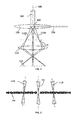
- Figure 1 schematically shows a part of a transmission electron microscope.
- the beam of electrons is formed by an electron source (not shown) and turned in a parallel beam by condenser optics (not shown).
- the condenser optics can vary the diameter of the beam.
- the beam then impinges on the sample 104, that is positioned in the objective lens 108 by positioning unit 106. Due to the wave nature of electrons part of the electrons are scattered by the sample in beams 112A and 112B. These beams, and the central beam of unscattered electrons is focused in the diffraction plane 114. In the diffraction plane thus a Fourier representation of the sample is available.
- the diffraction plane is imaged by the diffraction lens 110, forming an enlarged image of the sample in image plane 116.
- Figure 2 schematically shows a Zernike phase plate.
- the Zernike phase plate consists of a thin film 200 of a material with a small hole.
- the diameter of the hole is typically 1 ⁇ m or less, and the material typically carbon.
- the wavelength of the electrons while passing through the carbon is shorter than when passing through vacuum.
- the contrast transfer function is high, opposed to the situation that would occur when the phase shift was not introduced: then the contrast transfer function would be zero, assuming there are no optical aberrations in the system.
- phase plate is positioned in the diffraction plane on a high precision holder.
- phase plate is not placed in the diffraction plane, but in an image of that plane, preferably an enlarged image, thereby making it easier to position the phase plate.
- Figure 3 schematically shows a layer of nano-crystalline carbon.
- the lattice of NCC is built from hexagons of carbon atoms, the atoms here represented as dots.
- the atoms are in one plane (graphite has many planes stacked on top of each other).
- the smaller distance of d 1 results in a smaller circle 402 in the diffraction pattern shown in figures 4A and 4B
- the smaller distance of d 2 results in the larger circle 404 in the diffraction pattern shown in figures 4A and 4B .
- Figure 4A shows the diffraction pattern of an amorphous thin film.
- a diffuse ring 402 represents electrons that are scattered at structures with a mutual distance of approximately 0,22 nm. Ring 402 is not sharply defined, indicating that there is a relative large variation on the mutual distance of these structures, as can be expected for amorphous material: there is no or little order. That the ring does not show points or arcs with larger intensity implies that there is no rotational preference of the scattering, another feature of amorphous material.
- Ring 404 represents the smaller lattice distance d 2 of approximately 0,122 nm.
- Object 406 is (the image of) the intercept needle blocking the central beam so as to avoid over-illumination and/or damage to the image sensor.
- Figure 4B shows the diffraction pattern of the thin film after treatment.
- the rings are much better defined. Careful analysis of the diffraction pattern showed rings corresponding to lattice distances of 0,211 nm (100%), 0,122 nm (50%), 0,107 nm (7 %), and peaks at 0.081, 0,071 and 0,062 nm (all at less than 5%).
- Figure 5A shows an amorphous carbon film with "footprints”.
- Figure 5A shows an amorphous carbon film 500 with perforations 502. On the film a beam of electrons has impinged, resulting in "footprints” 504. These "footprints” are believed to result from a (temporary) change in electronic structure in the carbon film, and disappear in approximately 1 day.
- Figure 5B shows a laser treated carbon film.
- the film shown in figure 5B is in origin identical to the film shown in figure 5A , but this film is laser treated. No "footprints" are visible. However, the thermal treatment induced some mechanical deformation.
- the rings and central spot are much better defined.
- the rings 202 and 204 do not show any granularity, proving that many crystals are present with a random orientation with respect to each other. Experiments showed that this is the case even for a beam diameter of 100 nm, even for a beam diameter as small as 100 nm.
- the foil was heated with a laser beam having a power of 10 mW and a wave length of 785 nm heating a spot with a diameter of between 25 ⁇ m to 100 ⁇ m. It is estimated that, at these conditions and film thickness, the foil absorbed 10% of this power, resulting in an absorbed power density of between 0,78 MW/m 2 (spot diameter 100 ⁇ m) and 12 MW/m 2 (spot diameter 25 ⁇ m).
- the laser beam was turned off and the foil was allowed to cool down in the sample chamber (the chamber at room temperature) to room temperature. Afterwards the condition of the foil was inspected in a TEM, and the diffraction pattern of figure 4B was recorded.
- the film is cleaned before heating, as a film that is not heated is contaminated.
- a carbon contamination with carbon in another structure than amorphous carbon may results in a film with varying thickness, and it is suggested that a non-amorphous carbon film is also transformed into non-NCC carbon film.
- a focused laser beam will also crack mobile contaminants on the film surface, causing a large build-up of some kind of amorphous carbon (but not of the type wanted), and also leading a large local change in thickness. It appears that heating to 250 °C (the temperature of the heating holder) is optimal. Heating is thus preferably performed by pre-heating in vacuum to a temperature of approximately 250 °C.
- plasma cleaning is possible, but can easily change the thickness of the film through etching. This makes plasma cleaning a less preferred option for cleaning, but a candidate for fine-tuning the thickness of the thin film.
Landscapes
- Chemical & Material Sciences (AREA)
- Analytical Chemistry (AREA)
- Organic Chemistry (AREA)
- Life Sciences & Earth Sciences (AREA)
- General Life Sciences & Earth Sciences (AREA)
- Geology (AREA)
- Inorganic Chemistry (AREA)
- Physics & Mathematics (AREA)
- Engineering & Computer Science (AREA)
- Plasma & Fusion (AREA)
- Carbon And Carbon Compounds (AREA)
- Physical Vapour Deposition (AREA)
Priority Applications (5)
| Application Number | Priority Date | Filing Date | Title |
|---|---|---|---|
| EP13195596.5A EP2881970A1 (en) | 2013-12-04 | 2013-12-04 | Method of producing a freestanding thin film of nano-crystalline carbon |
| EP14195297.8A EP2881971B1 (en) | 2013-12-04 | 2014-11-28 | Method of producing a freestanding thin film of nano-crystalline graphite |
| JP2014244984A JP6224573B2 (ja) | 2013-12-04 | 2014-12-03 | ナノ結晶カーボン自立薄膜の製造方法 |
| US14/560,919 US9908778B2 (en) | 2013-12-04 | 2014-12-04 | Method of producing a freestanding thin film of nano-crystalline graphite |
| CN201410726248.6A CN104701122A (zh) | 2013-12-04 | 2014-12-04 | 产生纳米结晶石墨的独立式薄膜方法 |
Applications Claiming Priority (1)
| Application Number | Priority Date | Filing Date | Title |
|---|---|---|---|
| EP13195596.5A EP2881970A1 (en) | 2013-12-04 | 2013-12-04 | Method of producing a freestanding thin film of nano-crystalline carbon |
Publications (1)
| Publication Number | Publication Date |
|---|---|
| EP2881970A1 true EP2881970A1 (en) | 2015-06-10 |
Family
ID=49752992
Family Applications (2)
| Application Number | Title | Priority Date | Filing Date |
|---|---|---|---|
| EP13195596.5A Withdrawn EP2881970A1 (en) | 2013-12-04 | 2013-12-04 | Method of producing a freestanding thin film of nano-crystalline carbon |
| EP14195297.8A Active EP2881971B1 (en) | 2013-12-04 | 2014-11-28 | Method of producing a freestanding thin film of nano-crystalline graphite |
Family Applications After (1)
| Application Number | Title | Priority Date | Filing Date |
|---|---|---|---|
| EP14195297.8A Active EP2881971B1 (en) | 2013-12-04 | 2014-11-28 | Method of producing a freestanding thin film of nano-crystalline graphite |
Country Status (4)
| Country | Link |
|---|---|
| US (1) | US9908778B2 (enExample) |
| EP (2) | EP2881970A1 (enExample) |
| JP (1) | JP6224573B2 (enExample) |
| CN (1) | CN104701122A (enExample) |
Families Citing this family (4)
| Publication number | Priority date | Publication date | Assignee | Title |
|---|---|---|---|---|
| US9953802B2 (en) * | 2014-01-21 | 2018-04-24 | Ramot At Tel-Aviv University Ltd. | Method and device for manipulating particle beam |
| WO2017183697A1 (ja) * | 2016-04-21 | 2017-10-26 | 株式会社カネカ | 放射性同位元素製造用の支持基板、放射性同位元素製造用ターゲット板、及び支持基板の製造方法 |
| CN107481913B (zh) * | 2016-06-08 | 2019-04-02 | 清华大学 | 一种电子束加工系统 |
| US20210087403A1 (en) * | 2019-09-20 | 2021-03-25 | Merck Patent Gmbh | Pigments |
Citations (4)
| Publication number | Priority date | Publication date | Assignee | Title |
|---|---|---|---|---|
| EP1640482A1 (en) * | 2003-05-30 | 2006-03-29 | Japan Science and Technology Agency | Process for producing extremely flat microcrystalline diamond thin film by laser ablation method |
| US20110200787A1 (en) * | 2010-01-26 | 2011-08-18 | The Regents Of The University Of California | Suspended Thin Film Structures |
| US20120261588A1 (en) * | 2011-04-14 | 2012-10-18 | Hon Hai Precision Industry Co., Ltd. | Transmission electron microscope micro-grid |
| EP2626885A1 (en) * | 2012-02-13 | 2013-08-14 | FEI Company | Forming a vitrified sample for an electron microscopy |
Family Cites Families (17)
| Publication number | Priority date | Publication date | Assignee | Title |
|---|---|---|---|---|
| EP2248645A1 (en) * | 1999-04-07 | 2010-11-10 | GrafTech International Holdings Inc. | Flexible graphite article and method of manufacture |
| EP2091062A1 (en) | 2008-02-13 | 2009-08-19 | FEI Company | TEM with aberration corrector and phase plate |
| EP2131385A1 (en) | 2008-06-05 | 2009-12-09 | FEI Company | Hybrid phase plate |
| US7977633B2 (en) | 2008-08-27 | 2011-07-12 | Max-Planck-Gesellschaft Zur Foerderung Der Wissenschaften E. V. | Phase plate, in particular for an electron microscope |
| JPWO2010090343A1 (ja) * | 2009-02-05 | 2012-08-09 | 帝人株式会社 | 黒鉛化炭素片分散液およびその製造方法 |
| CN101964291B (zh) * | 2009-07-24 | 2012-03-28 | 清华大学 | 透射电镜微栅及其制备方法 |
| CA2789028C (en) * | 2010-02-19 | 2016-01-05 | Incubation Alliance, Inc. | Carbon material and method for producing same |
| TWI417934B (zh) | 2010-03-26 | 2013-12-01 | Hon Hai Prec Ind Co Ltd | 透射電鏡微柵的製備方法 |
| WO2012094634A2 (en) * | 2011-01-07 | 2012-07-12 | Dune Sciences, Inc. | Functionalized carbon membranes |
| EP2485239A1 (en) | 2011-02-07 | 2012-08-08 | FEI Company | Method for centering an optical element in a TEM comprising a contrast enhancing element |
| DE102011014399B4 (de) * | 2011-03-18 | 2017-08-03 | Stiftung Caesar Center Of Advanced European Studies And Research | Phasenplatte, Verfahren zum Herstellen einer Phasenplatte sowie Elektronenmikroskop |
| JP5812342B2 (ja) * | 2011-12-12 | 2015-11-11 | 東海カーボン株式会社 | グラファイトフィルムの製造方法 |
| JP6212050B2 (ja) * | 2011-12-22 | 2017-10-11 | スリーエム イノベイティブ プロパティズ カンパニー | 高い光透過を備えた導電性物品 |
| EP2667399A1 (en) * | 2012-05-23 | 2013-11-27 | FEI Company | Improved phase plate for a TEM |
| EP2704178B1 (en) | 2012-08-30 | 2014-08-20 | Fei Company | Imaging a sample in a TEM equipped with a phase plate |
| JP6286270B2 (ja) | 2013-04-25 | 2018-02-28 | エフ イー アイ カンパニFei Company | 透過型電子顕微鏡内で位相版を用いる方法 |
| DE102013019297A1 (de) | 2013-11-19 | 2015-05-21 | Fei Company | Phasenplatte für ein Transmissionselektronenmikroskop |
-
2013
- 2013-12-04 EP EP13195596.5A patent/EP2881970A1/en not_active Withdrawn
-
2014
- 2014-11-28 EP EP14195297.8A patent/EP2881971B1/en active Active
- 2014-12-03 JP JP2014244984A patent/JP6224573B2/ja active Active
- 2014-12-04 CN CN201410726248.6A patent/CN104701122A/zh active Pending
- 2014-12-04 US US14/560,919 patent/US9908778B2/en active Active
Patent Citations (4)
| Publication number | Priority date | Publication date | Assignee | Title |
|---|---|---|---|---|
| EP1640482A1 (en) * | 2003-05-30 | 2006-03-29 | Japan Science and Technology Agency | Process for producing extremely flat microcrystalline diamond thin film by laser ablation method |
| US20110200787A1 (en) * | 2010-01-26 | 2011-08-18 | The Regents Of The University Of California | Suspended Thin Film Structures |
| US20120261588A1 (en) * | 2011-04-14 | 2012-10-18 | Hon Hai Precision Industry Co., Ltd. | Transmission electron microscope micro-grid |
| EP2626885A1 (en) * | 2012-02-13 | 2013-08-14 | FEI Company | Forming a vitrified sample for an electron microscopy |
Non-Patent Citations (6)
| Title |
|---|
| "Internet brochure", 14 August 2007, ARIZONA CARBON FOIL CO., INC |
| "Page of internet sales brochure", AGAR SCIENTIFIC |
| B. J. MCMORRAN ET AL.: "Electron Vortex Beams with High Quanta of Orbital Angular Momentum", SCIENCE, vol. 331, no. 192, 2011, pages 192 - 195 |
| GRAPHENE LABS: "Graphene Transmission Electron Microscopy Support Films", 23 December 2011 (2011-12-23), XP055115586, Retrieved from the Internet <URL:http://www.graphene-supermarket.com/images/XC/TEM/GrapheneTEMgrids-General info.pdf> [retrieved on 20140428] * |
| J. ROBERTSON: "Diamond-like amorphous carbon", MATERIALS SCIENCE AND ENGINEERING R37, 2002, pages 129 - 281 |
| K. NAGAYAMA ET AL.: "Phase Contrast Enhancement with Phase Plates in Biological Electron Microscopy", MICROSCOPY TODAY, vol. 18, no. 4, July 2010 (2010-07-01), pages 10 - 13 |
Also Published As
| Publication number | Publication date |
|---|---|
| CN104701122A (zh) | 2015-06-10 |
| EP2881971A1 (en) | 2015-06-10 |
| JP2015107913A (ja) | 2015-06-11 |
| US20160096734A2 (en) | 2016-04-07 |
| EP2881971B1 (en) | 2017-01-04 |
| US9908778B2 (en) | 2018-03-06 |
| JP6224573B2 (ja) | 2017-11-01 |
| US20150151972A1 (en) | 2015-06-04 |
Similar Documents
| Publication | Publication Date | Title |
|---|---|---|
| JP4189770B2 (ja) | X線用ターゲット及びそれを用いた装置 | |
| CA2285296C (en) | High resolution x-ray imaging of very small objects | |
| Salomé et al. | The ID21 scanning X-ray microscope at ESRF | |
| US9129774B2 (en) | Method of using a phase plate in a transmission electron microscope | |
| EP2881971B1 (en) | Method of producing a freestanding thin film of nano-crystalline graphite | |
| Egerton | An introduction to microscopy | |
| Wang et al. | Atomic-scale structure analysis by advanced transmission electron microscopy | |
| Hummell et al. | Design and fabrication of multi-metal patterned target anodes for improved quality of hyperspectral x-ray radiography and computed tomography imaging systems | |
| Baksh et al. | Quantitative evaluation of hard x-ray damage to biological samples using EUV ptychography | |
| Wang et al. | Fabrication of nanoscale patterns in lithium fluoride crystal using a 13.5 nm Schwarzschild objective and a laser produced plasma source | |
| JP6636061B2 (ja) | Tem内での特徴のない薄膜の位置合わせ | |
| Peppernick et al. | Near-field focused photoemission from polystyrene microspheres studied with photoemission electron microscopy | |
| Liu et al. | Nanofabrication and characterization of a grating-based condenser for uniform illumination with hard X-rays | |
| Schneider et al. | Novel X-ray microscopes for 3-D and fs-imaging at BESSY | |
| Vallières et al. | Laser-driven proton acceleration with nanostructured targets | |
| Kliuiev | Reconstruction of molecular orbitals from photoemission data with iterative phase retrieval algorithms | |
| AU747809B2 (en) | High resolution X-ray imaging of very small objects | |
| Fardin et al. | Quantitative phase nano-imaging with a laboratory source | |
| Kawasaki et al. | Convenient optics for high dispersion small angle electron diffraction with highly coherent low dose illumination | |
| Farahani | Structural modification of solids by ultra-short X-ray laser pulses | |
| Torrisi et al. | Nanoscale imaging and optimization of a compact" water window" SXR microscope | |
| Dinh et al. | Coherent Diffractive Imaging Using Table-top High Harmonic Generation | |
| Dinh et al. | Coherent diffractive imaging of single layer microspheres | |
| Pearmain | Electron microscopy characterisation of size-selected Pd clusters and industrial Pd catalysts | |
| Gardner Jr | Coherent Diffractive Imaging Near the Spatio-Temporal Limit with High-Harmonic Sources |
Legal Events
| Date | Code | Title | Description |
|---|---|---|---|
| PUAI | Public reference made under article 153(3) epc to a published international application that has entered the european phase |
Free format text: ORIGINAL CODE: 0009012 |
|
| 17P | Request for examination filed |
Effective date: 20131204 |
|
| AK | Designated contracting states |
Kind code of ref document: A1 Designated state(s): AL AT BE BG CH CY CZ DE DK EE ES FI FR GB GR HR HU IE IS IT LI LT LU LV MC MK MT NL NO PL PT RO RS SE SI SK SM TR |
|
| AX | Request for extension of the european patent |
Extension state: BA ME |
|
| STAA | Information on the status of an ep patent application or granted ep patent |
Free format text: STATUS: THE APPLICATION IS DEEMED TO BE WITHDRAWN |
|
| 18D | Application deemed to be withdrawn |
Effective date: 20151211 |