EP2879194A1 - Light emitting diode package, light source module and backlight unit including the same - Google Patents
Light emitting diode package, light source module and backlight unit including the same Download PDFInfo
- Publication number
- EP2879194A1 EP2879194A1 EP14169951.2A EP14169951A EP2879194A1 EP 2879194 A1 EP2879194 A1 EP 2879194A1 EP 14169951 A EP14169951 A EP 14169951A EP 2879194 A1 EP2879194 A1 EP 2879194A1
- Authority
- EP
- European Patent Office
- Prior art keywords
- emitting diode
- light emitting
- lead
- chain structure
- case
- Prior art date
- Legal status (The legal status is an assumption and is not a legal conclusion. Google has not performed a legal analysis and makes no representation as to the accuracy of the status listed.)
- Granted
Links
Images


Classifications
-
- H—ELECTRICITY
- H10—SEMICONDUCTOR DEVICES; ELECTRIC SOLID-STATE DEVICES NOT OTHERWISE PROVIDED FOR
- H10H—INORGANIC LIGHT-EMITTING SEMICONDUCTOR DEVICES HAVING POTENTIAL BARRIERS
- H10H20/00—Individual inorganic light-emitting semiconductor devices having potential barriers, e.g. light-emitting diodes [LED]
- H10H20/80—Constructional details
- H10H20/85—Packages
- H10H20/857—Interconnections, e.g. lead-frames, bond wires or solder balls
-
- G—PHYSICS
- G02—OPTICS
- G02B—OPTICAL ELEMENTS, SYSTEMS OR APPARATUS
- G02B6/00—Light guides; Structural details of arrangements comprising light guides and other optical elements, e.g. couplings
- G02B6/0001—Light guides; Structural details of arrangements comprising light guides and other optical elements, e.g. couplings specially adapted for lighting devices or systems
- G02B6/0011—Light guides; Structural details of arrangements comprising light guides and other optical elements, e.g. couplings specially adapted for lighting devices or systems the light guides being planar or of plate-like form
- G02B6/0066—Light guides; Structural details of arrangements comprising light guides and other optical elements, e.g. couplings specially adapted for lighting devices or systems the light guides being planar or of plate-like form characterised by the light source being coupled to the light guide
- G02B6/0068—Arrangements of plural sources, e.g. multi-colour light sources
-
- G—PHYSICS
- G02—OPTICS
- G02B—OPTICAL ELEMENTS, SYSTEMS OR APPARATUS
- G02B6/00—Light guides; Structural details of arrangements comprising light guides and other optical elements, e.g. couplings
- G02B6/0001—Light guides; Structural details of arrangements comprising light guides and other optical elements, e.g. couplings specially adapted for lighting devices or systems
- G02B6/0011—Light guides; Structural details of arrangements comprising light guides and other optical elements, e.g. couplings specially adapted for lighting devices or systems the light guides being planar or of plate-like form
- G02B6/0066—Light guides; Structural details of arrangements comprising light guides and other optical elements, e.g. couplings specially adapted for lighting devices or systems the light guides being planar or of plate-like form characterised by the light source being coupled to the light guide
- G02B6/0073—Light emitting diode [LED]
-
- G—PHYSICS
- G02—OPTICS
- G02B—OPTICAL ELEMENTS, SYSTEMS OR APPARATUS
- G02B6/00—Light guides; Structural details of arrangements comprising light guides and other optical elements, e.g. couplings
- G02B6/0001—Light guides; Structural details of arrangements comprising light guides and other optical elements, e.g. couplings specially adapted for lighting devices or systems
- G02B6/0011—Light guides; Structural details of arrangements comprising light guides and other optical elements, e.g. couplings specially adapted for lighting devices or systems the light guides being planar or of plate-like form
- G02B6/0081—Mechanical or electrical aspects of the light guide and light source in the lighting device peculiar to the adaptation to planar light guides, e.g. concerning packaging
- G02B6/0083—Details of electrical connections of light sources to drivers, circuit boards, or the like
-
- H—ELECTRICITY
- H10—SEMICONDUCTOR DEVICES; ELECTRIC SOLID-STATE DEVICES NOT OTHERWISE PROVIDED FOR
- H10H—INORGANIC LIGHT-EMITTING SEMICONDUCTOR DEVICES HAVING POTENTIAL BARRIERS
- H10H20/00—Individual inorganic light-emitting semiconductor devices having potential barriers, e.g. light-emitting diodes [LED]
- H10H20/80—Constructional details
- H10H20/85—Packages
-
- H—ELECTRICITY
- H10—SEMICONDUCTOR DEVICES; ELECTRIC SOLID-STATE DEVICES NOT OTHERWISE PROVIDED FOR
- H10H—INORGANIC LIGHT-EMITTING SEMICONDUCTOR DEVICES HAVING POTENTIAL BARRIERS
- H10H20/00—Individual inorganic light-emitting semiconductor devices having potential barriers, e.g. light-emitting diodes [LED]
- H10H20/80—Constructional details
- H10H20/85—Packages
- H10H20/8506—Containers
-
- H—ELECTRICITY
- H10—SEMICONDUCTOR DEVICES; ELECTRIC SOLID-STATE DEVICES NOT OTHERWISE PROVIDED FOR
- H10H—INORGANIC LIGHT-EMITTING SEMICONDUCTOR DEVICES HAVING POTENTIAL BARRIERS
- H10H29/00—Integrated devices, or assemblies of multiple devices, comprising at least one light-emitting semiconductor element covered by group H10H20/00
- H10H29/10—Integrated devices comprising at least one light-emitting semiconductor component covered by group H10H20/00
- H10H29/14—Integrated devices comprising at least one light-emitting semiconductor component covered by group H10H20/00 comprising multiple light-emitting semiconductor components
-
- H—ELECTRICITY
- H10—SEMICONDUCTOR DEVICES; ELECTRIC SOLID-STATE DEVICES NOT OTHERWISE PROVIDED FOR
- H10W—GENERIC PACKAGES, INTERCONNECTIONS, CONNECTORS OR OTHER CONSTRUCTIONAL DETAILS OF DEVICES COVERED BY CLASS H10
- H10W90/00—Package configurations
- H10W90/701—Package configurations characterised by the relative positions of pads or connectors relative to package parts
- H10W90/751—Package configurations characterised by the relative positions of pads or connectors relative to package parts of bond wires
- H10W90/756—Package configurations characterised by the relative positions of pads or connectors relative to package parts of bond wires between a chip and a stacked lead frame, conducting package substrate or heat sink
Definitions
- the present disclosure relates to a light emitting diode package, and particularly, to a light emitting diode package capable of reducing a size of a light source module by forming an additional line therein, a light source module and a backlight unit including the same.
- a liquid crystal display (LCD) device has a small thickness, a light weight, and low power consumption. Owing to such advantages, the LCD device is applied to a large television, etc., as well as a monitor, a notebook computer and a portable phone.
- Such LCD device includes a liquid crystal (LC) panel configured to display an image using an optical transmittance of liquid crystal molecules, and a backlight unit disposed below the LC panel and providing light to the LC panel.
- LC liquid crystal
- the backlight unit includes a light source module configured to generate light to be provided to the LC panel.
- a light source of the light source module may include a Cold Cathode Fluorescent Lamp (CCFL), a Flat Fluorescent Lamp (FFL), a Light Emitting Diode (LED), etc.
- the LED has characteristics of high light-emitting efficiency, long lifespan and low power consumption. Due to such characteristics, the LED is used as a light source of the light source module of the backlight unit.
- the LED is fabricated in the form of packages in which light emitting chips have been mounted, and is used as a light source of the light source module.
- FIG. 1A is a schematic view illustrating a configuration of a light emitting diode (LED) package in accordance with the conventional art
- FIG. 1B is a sectional view taken along line I-I' in FIG. 1A .
- the conventional LED package 1 includes a lead frame 6 composed of two leads separated from each other, i.e., an anode lead 6a and a cathode lead 6b; and a LED chip 4 mounted on one surface of the lead frame 6.
- the LED chip 4 is connected to the anode lead 6a and the cathode lead 6b of the lead frame 6, by a wire 5 formed of gold (Au), silver (Ag), etc.
- the lead frame 6, the LED chip 4 and the wire 5 are enclosed by the case 2 formed of opaque resin, etc. Part of the anode lead 6a and the cathode lead 6b of the lead frame 6 is exposed to outside so as to be mounted on a printed circuit board (not shown).
- the LED chip 4 enclosed by the case 2 is covered by a sealant 3 formed of transparent resin.
- FIG. 2 is a view schematically illustrating a light source module in accordance with the conventional art.
- a plurality of LED packages 1 are mounted on a printed circuit board 11, to thus constitute a light source module 10.
- the plurality of LED packages 1 are implemented in the form of groups, which are called chains.
- an odd-numbered LED package 1 and an even-numbered LED package 1 among the plurality of LED packages 1 mounted on the printed circuit board 11 are arranged in groups with two chain structures.
- the light source module 10 has a plurality of LED packages 1 mounted on the printed circuit board 11 in groups with a first chain structure and a second chain structure. Each group is connected to lines formed at the printed circuit board 11, i.e., power supply lines 13a, 13b and connection lines 14a, 14b.
- the first chain structure is composed of a first LED package 1 connected to the first power supply line 13a of the printed circuit board 11, a third LED package 1 connected to the first LED package 1 by the first connection line 14a, and a fifth LED package 1.
- the second chain structure is composed of a second LED package 1 connected to the second power supply line 13b of the printed circuit board 11, and a fourth LED package 1 connected to the second LED package 1 by the second connection line 14b.
- the plurality of LED packages 1 having the first chain structure, and the plurality of LED packages 1 having the second chain structure are mounted on the printed circuit board 11 so that electrodes thereof can alternate each other in polarity.
- the first LED package 1 having the first chain structure has electrodes (+), (-)
- the third LED package 1 connected to the first LED package 1 through the first connection line 14a has electrodes (-), (+).
- the fifth LED package 1 connected to the third LED package 1 through the first connection line 14a has electrodes (+), (-).
- the plurality of LED packages 1 having the first chain structure are connected to one another in serial.
- the second chain structure is implemented in the same manner as the first chain structure.
- the first chain structure and the second chain structure are implemented in parallel.
- the second connection line 14b should be formed at an upper end or a lower end of the LED package 1 having the first chain structure. Under such configuration, the width (D) of the printed circuit board 11 is increased.
- the printed circuit board 11 of the light source module 10 has a multi-layered structure. Accordingly, lines are formed even on a rear surface of the printed circuit board 11. Lines formed on a front surface of the printed circuit board 11 are connected to lines formed on a rear surface of the printed circuit board 11, through holes 15. As the number of chain structures is increased, the number of lines formed on the rear surface of the printed circuit board 11, and the length of the lines are increased.
- the light source module 10 is accommodated in a side wall of an accommodating container(not shown) of the LCD device. As the LCD device becomes slim, the printed circuit board 11 of the light source module 10 has a limited width.
- the width (D) of the printed circuit board 11 is increased.
- the printed circuit board 11 having a multi-layered structure is used.
- production cost of the light source module 10 is increased.
- an aspect of the detailed description is to provide a light emitting diode package capable of reducing a width of a printed circuit board of a light source module, by forming a line therein, a light source module and a backlight unit including the same.
- a light emitting diode (LED) package comprising: a light emitting diode chip configured to generate light; a case configured to accommodate therein the light emitting diode chip; lead frames spaced from each other in the case, and having an anode lead and a cathode lead electrically-connected to the light emitting diode chip; and at least one dummy lead frame spaced from the lead frames in an insulated state to form a line.
- LED light emitting diode
- the at least one dummy lead frame comprises at least two leads spaced from each other and electrically connected to each other in the case.
- the dummy lead frame comprises: a first dummy lead spaced from the anode lead; and a second dummy lead spaced from the cathode lead, and connected to the first dummy lead in the case through a wire.
- one end of the anode lead and one end of the cathode lead are exposed from two sides of the case, wherein one end of the first dummy lead is exposed from one side of the case to thus be spaced from the anode lead, and one end of the second dummy lead is exposed from another side of the case to thus be spaced from the cathode lead.
- the dummy lead frame includes: a first dummy lead and a third dummy lead spaced from the anode lead; a second dummy lead spaced from the cathode lead, and connected to the first dummy lead in the case through a first wire; and a fourth dummy lead spaced from the cathode lead and the second dummy lead, and connected to the third dummy lead in the case through a second wire.
- one end of the anode lead and one end of the cathode lead are exposed from two sides of the case, and wherein one end of the first dummy lead and one end of the third dummy lead are exposed from one side of the case, to thus face each other in a state where the anode lead is interposed therebetween, and wherein one end of the second dummy lead and one end of the fourth dummy lead are exposed from another side of the case, to thus face each other in a state where the cathode lead is interposed therebetween.
- the dummy lead frame is extending from one side of the case to another side of the case through inside of the case, to thus be integrally formed, and wherein the dummy lead frame is spaced from the lead frame.
- the dummy lead frame is extending from one side of the case to another side of the case through an outer surface of the case, to thus be integrally formed.
- a light source module comprising: a printed circuit board; and a plurality of light emitting diode packages according to one or more embodiments described herein that are mounted sequentially arranged on the printed circuit board, having a first chain structure and a second chain structure, wherein an output of one light emitting diode package having the first chain structure is connected to another light emitting diode package having the first chain structure, through the dummy lead frame of an adjacent light emitting diode package having the second chain structure.
- an output of a first light emitting diode package having the first chain structure is connected to a third light emitting diode package having the first chain structure, through the dummy lead frame of a second light emitting diode package having the second chain structure.
- an output of a second light emitting diode package having the second chain structure is connected to a fourth light emitting diode package having the second chain structure, through the dummy lead frame of a third light emitting diode package having the first chain structure.
- the light source module further comprises: a first connection line formed on the printed circuit board, and configured to connect an output of the plurality of light emitting diode packages having the first chain structure, to the dummy lead frame of the plurality of light emitting diode packages having the second chain structure; and a second connection line formed on the printed circuit board, and configured to connect an output of the plurality of light emitting diode packages having the second chain structure, to the dummy lead frame of the plurality of light emitting diode packages having the first chain structure.
- the plurality of light emitting diode packages having the respective chain structures are arranged on the printed circuit board, such that electrodes thereof alternate each other in polarity.
- a light source module comprising: a printed circuit board; and a plurality of light emitting diode packages according to one or more embodiments described herein that are mounted sequentially arranged on the printed circuit board, having a first chain structure, a second chain structure and a third chain structure, wherein an output of one light emitting diode package having the first chain structure is connected to another light emitting diode package having the first chain structure, through the dummy lead frame of an adjacent light emitting diode package having the second chain structure and the dummy lead frame of the light emitting diode package having the third chain structure.
- a backlight unit comprising: a light source module according to one or more embodiments described herein; a light guiding plate arranged at one side of the light source module, and configured to guide light generated from the light source module; and an accommodation container configured to accommodate therein the light source module and the light guiding plate.
- a light emitting diode package comprising: a light emitting diode chip configured to generate light; a case configured to accommodate therein the light emitting diode chip; lead frames spaced from each other in the case, and having an anode lead and a cathode lead electrically-connected to the light emitting diode chip; and at least one dummy lead frame spaced from the lead frames in an insulated state, and connected to each other in the case to form a line.
- a light source module comprising: a printed circuit board; and a plurality of light emitting diode packages are mounted sequentially arranged on the printed circuit board, having a first chain structure and a second chain structure, wherein each of the plurality of light emitting diode packages including light emitting diode chip configured to generate light, a case configured to accommodate therein the light emitting diode chip, lead frames spaced from each other in the case, and having an anode lead and a cathode lead electrically-connected to the light emitting diode chip, and at least one dummy lead frame spaced from the lead frames in an insulated state, and connected to each other in the case to form a line.
- An output of one light emitting diode package having the first chain structure may be connected to another light emitting diode package having the first chain structure, through the dummy lead frame of an adjacent light emitting diode package having the second chain structure.
- a backlight unit comprising: a light source module; a light guiding plate arranged at one side of the light source module, and configured to guide light generated from the light source module; and an accommodation container configured to accommodate therein the light source module and the light guiding plate.
- the LED package, the light source module and the backlight unit including the same according to the present invention can have the following advantages.
- the plurality of LED packages can be mounted on the PCB without interference therebetween, by using at least one line formed therein. This can reduce a width of the PCB of the light source module, and reduce production cost of the light source module.
- a light emitting diode (LED) package, a light source module and a backlight unit according to the present invention will be explained in more detail with reference to the attached drawings.
- a liquid crystal display (LCD) device will be explained for convenience.
- the present invention may be applicable not only to a LCD device, but also to various flat display devices using a backlight unit.
- FIG. 3 is a view schematically illustrating a configuration of a light emitting diode (LED) package according to a first embodiment of the present invention
- FIG. 4 is a perspective view of the LED package of FIG. 3 .
- LED light emitting diode
- the LED package 100 may include a case 110, lead frames 131, 133, dummy lead frames 141, 143, and a LED chip 120.
- the case 110 may be formed to have a 'U'-shape such that an upper surface is open.
- the case 110 may have an accommodation space for accommodating therein the lead frames 131, 133, the dummy lead frames 141, 143, and the LED chip 120.
- the case 110 may be formed of an insulating material such as polymer or ceramic, in order to insulate and protect the components accommodated therein.
- a sealant (not shown), formed of a transparent resin, etc. in order to diffuse light generated from the LED chip 120, may be filled in the case 110.
- a reflecting material (not shown) may be coated on an inner side surface of the case 110.
- the lead frames 131, 133 may include an anode lead 131 and a cathode lead 133.
- the anode lead 131 and the cathode lead 133 may be arranged at two sides of the case 110, so as to correspond to each other.
- the anode lead 131 and the cathode lead 133 may be electrically-insulated from each other in the case 110, in a spaced state from each other.
- each of the anode lead 131 and the cathode lead 133 may be exposed to outside of the case 110.
- one end of the anode lead 131 may be exposed to outside from one side wall of the case 110
- one end of the cathode lead 133 may be exposed to outside from another side wall of the case 110.
- the LED chip 120 may be mounted on the anode lead 131 in the case 110.
- the LED chip 120 may be mounted on the anode lead 131 in a die-bonding manner by conductive epoxy.
- the present invention is not limited to this. In some cases, the LED chip 120 may be mounted on the cathode lead 133.
- the LED chip 120 may be electrically-connected to each of the anode lead 131 and the cathode lead 133, through a first wire 135.
- an n-type electrode of the LED chip 120 i.e., an anode terminal may be connected to the anode lead 131 through the first wire 135.
- a p-type electrode of the LED chip 120 i.e., a cathode terminal may be connected to the cathode lead 133 through the first wire 135.
- the LED chip 120 may be composed of an n-type semiconductor layer, a p-type semiconductor layer, a light emitting layer formed between the two semiconductor layers, an n-type electrode connected to the n-type semiconductor layer, and a p-type electrode connected to the p-type semiconductor layer.
- the LED chip 120 may be a GaN or GaN/AlGaN-based n-type semiconductor layer implemented as n-type semiconductor impurities have been doped on a substrate (not shown) formed of a transparent material such as sapphire, gallium nitride (GaN) and silicon carbide (SiC).
- the n-type semiconductor impurities may be silicon (Si), germanium (Ge) or tin (Sn).
- a light emitting layer may be formed on the n-type semiconductor layer.
- the light emitting layer may be formed of a GaN-based material, and may have a single quantum well (SQW) structure or a multi quantum well (MQW) structure.
- SQW single quantum well
- MQW multi quantum well
- the p-type semiconductor impurities may be magnesium (Mg).
- the p-type semiconductor layer and the light emitting layer may be etched so that the n-type semiconductor layer can be partially exposed to outside.
- the n-type electrode may be formed on the n-type semiconductor layer exposed to outside by such etching.
- the p-type electrode may be formed on the p-type semiconductor layer having not been etched.
- an electron and a hole may be provided to the light emitting layer from the n-type semiconductor layer and the p-type semiconductor layer. While the electron and the hole are re-coupled to each other at the light emitting layer, energy is generated. The energy may be converted into light, and the generated light may be emitted to outside.
- the dummy lead frames 141, 143 may be spaced from the lead frames 131, 133, and may be electrically-insulated from each other.
- the dummy lead frames 141, 143 may include a first dummy lead 141 and a second dummy lead 143.
- the first dummy lead 141 may be disposed at one side of the case 110, with a distance from the anode lead 131.
- the second dummy lead 142 may be disposed at another side of the case 110, with a distance from the cathode lead 133.
- the first dummy lead 141 and the second dummy lead 143 may be electrically-insulated from each other, in a spaced state from each other in the case 110.
- each of the first dummy lead 141 and the second dummy lead 143 may be exposed to outside of the case 110.
- one end of the first dummy lead 141 may be exposed to outside from one side wall of the case 110
- one end of the second dummy lead 143 may be exposed to outside from another side wall of the case 110.
- the exposed end of the first dummy lead 141 and the exposed end of the second dummy lead 143 may correspond to each other at two sides of the case 110.
- the first dummy lead 141 and the second dummy lead 143 may be electrically-connected to each other in the case 110, through a second wire 145. More specifically, the first dummy lead 141 and the second dummy lead 143 are spaced from the lead frames 131, 133 in an insulated state from each other, and are connected to each other by the second wire 145. Accordingly, the first dummy lead 141 and the second dummy lead 143 may be formed as a single line in the LED package 100.
- the LED package 100 according to the first embodiment of the present invention is provided therein with the dummy lead frames 141, 143 serving as additional lines. Accordingly, in a case where a plurality of LED packages 100 are mounted on a printed circuit board (PCB) of a light source module to be explained later, the number of lines formed on the PCB, or the length of the line can be reduced.
- PCB printed circuit board
- FIG. 5 is a view schematically illustrating a configuration of a light emitting diode (LED) package according to a second embodiment of the present invention
- FIG. 6 is a perspective view of the LED package of FIG. 5 .
- LED light emitting diode
- the LED package 101 may include a case 110, lead frames 131, 133, first dummy lead frames 141, 143, second dummy lead frames 151, 153 and a LED chip 120.
- the case 110 has an open upper surface, and accommodates therein the lead frames 131, 133, the first dummy lead frames 141, 143, the second dummy lead frames 151, 153 and the LED chip 120.
- a sealant may be filled in the case 110, and a reflecting material may be coated on an inner side surface of the case 110.
- the lead frames 131, 133 may include an anode lead 131 and a cathode lead 133.
- the anode lead 131 and the cathode lead 133 are arranged at two sides of the case 110 in correspondence to each other, and may be electrically-insulated from each other in a spaced state from each other in the case 110.
- One end of the anode lead 131 may be exposed to outside from one side wall of the case 110, and one end of the cathode lead 133 may be exposed to outside from another side wall of the case 110.
- the LED chip 120 may be mounted on the anode lead 131 in the case 110.
- the LED chip 120 may be electrically-connected to the anode lead 131 and the cathode lead 133 through the first wire 135.
- An anode terminal of the LED chip 120 may be connected to the anode lead 131 through the first wire 135, and a cathode terminal of the LED chip 120 may be connected to the cathode lead 133 through the first wire 135.
- Each of the first dummy lead frames 141, 143, and the second dummy lead frames 151, 153 may be spaced from the lead frames 131, 133, and may be electrically-insulated from each other.
- the first dummy lead frames 141, 143 may include a first dummy lead 141 and a second dummy lead 143.
- the second dummy lead frames 151, 153 may include a third dummy lead 151 and a fourth dummy lead 153.
- the first dummy lead 141 may be spaced from the anode lead 131 at one side of the case 110.
- the second dummy lead 143 may be spaced from the cathode lead 133 at another side of the case 110.
- the first dummy lead 141 and the second dummy lead 143 may be spaced from each other to thus be electrically-insulated from each other in the case 110.
- the third dummy lead 151 may be spaced from the anode lead 131 and the first dummy lead 141 at one side of the case 110.
- the fourth dummy lead 153 may be spaced from the cathode lead 133 and the second dummy lead 143 at another side of the case 110.
- the third dummy lead 151 and the fourth dummy lead 153 may be spaced from each other to thus be electrically-insulated from each other in the case 110.
- the third dummy lead 151 may be arranged to face the first dummy lead 141 at one side of the case 110, in a state where the anode lead 131 is interposed between the first dummy lead 141 and the third dummy lead 151.
- the fourth dummy lead 153 may be arranged to face the second dummy lead 143 at another side of the case 110, in a state where the cathode lead 133 is interposed between the second dummy lead 143 and the fourth dummy lead 153.
- first dummy lead 141 may be exposed to outside of the case 110, and one end of the second dummy lead 143 may be exposed to outside of the case 110.
- the exposed end of the first dummy lead 141 and the exposed end of the second dummy lead 143 may correspond to each other at two sides of the case 110.
- One end of the third dummy lead 151 may be exposed to outside of the case 110, and one end of the fourth dummy lead 153 may be exposed to outside of the case 110.
- the exposed end of the third dummy lead 151 and the exposed end of the fourth dummy lead 153 may correspond to each other at two sides of the case 110.
- the exposed first dummy lead 141 and the exposed third dummy lead 151 may face each other at one side of the case 110, in a state where the exposed anode lead 131 is interposed therebetween.
- the exposed second dummy lead 143 and the exposed fourth dummy lead 153 may face each other at another side of the case 110, in a state where the exposed cathode lead 133 is interposed therebetween.
- the first dummy lead 141 and the second dummy lead 143 may be electrically-connected to each other in the case 110 through the second wire 145, and the third dummy lead 151 and the fourth dummy lead 153 may be electrically-connected to each other in the case 110 through a third line 155.
- first dummy lead 141 and the second dummy lead 143 may be connected to each other in the case 110 through the second wire 145, thereby forming one single line.
- the third dummy lead 151 and the fourth dummy lead 153 may be connected to each other in the case 110 through the third line 155, thereby forming another single line.
- the LED package 101 according to the second embodiment of the present invention is provided therein with two types of dummy lead frames serving as additional lines, i. e., the first dummy lead frames 141, 143 and the second dummy lead frames 151, 153.
- the LED package 100 is mounted on a printed circuit board (PCB)
- the number of lines formed on the PCB, or the length of the line can be reduced.
- FIG. 7 is a view schematically illustrating a configuration of a light emitting diode (LED) package according to a third embodiment of the resent invention
- FIG. 8 is a perspective view of the LED package of FIG. 7 .
- LED light emitting diode
- the LED package 102 according to the third embodiment is the same as the LED package 100 aforementioned with reference to FIGS. 3 and 4 , except that a dummy lead frame 160 is integrally formed with the LED package 102. Accordingly, detailed explanations on the same components will be omitted.
- the LED package 102 may include a case 110, lead frames 131, 133, a dummy lead frame 160 and a LED chip 120.
- the case 110 has an open upper surface, and accommodates therein the lead frames 131, 133, the dummy lead frame 160 and the LED chip 120.
- a sealant may be filled in the case 110, and a reflecting material may be coated on an inner side surface of the case 110.
- the lead frames 131, 133 may include an anode lead 131 and a cathode lead 133.
- the anode lead 131 and the cathode lead 133 may be arranged at two sides of the case 110, so as to correspond to each other.
- the anode lead 131 and the cathode lead 133 may be electrically-insulated from each other in the case 110, in a spaced state from each other.
- One end of the anode lead 131 may be exposed to outside from one side wall of the case 110, and one end of the cathode lead 133 may be exposed to outside from another side wall of the case 110.
- the LED chip 120 may be mounted on the anode lead 131 in the case 110.
- the LED chip 120 may be electrically-connected to the anode lead 131 and the cathode lead 133 through the first wire 135.
- An anode terminal of the LED chip 120 may be connected to the anode lead 131 through the first wire 135, and a cathode terminal of the LED chip 120 may be connected to the cathode lead 133 through the first wire 135.
- the dummy lead frame 160 may be extending from one side of the case 110 to another side of the case 110 through inside of the case 110, thereby being integrally formed.
- the dummy lead frame 160 may be spaced from the lead frames 131, 133, and may be insulated from the lead frames 131, 133.
- One side of the dummy lead frame 160 may be exposed to outside from one side wall of the case 110, and another side thereof may be exposed to outside from another side wall of the case 110.
- Said one exposed side of the dummy frame 160 may be spaced from the anode lead 131 at one side of the case 110.
- Said another exposed side of the dummy frame 160 may be spaced from the cathode lead 133 at another side of the case 110.
- Said one exposed side of the dummy frame 160 and said another exposed side of the dummy frame 160 may be may correspond to each other at two sides of the case 110.
- the LED package 102 according to the third embodiment is provided therein with the dummy lead frame 160 serving as an additional line.
- This can reduce the number of lines of a printed circuit board (PCB) on which the LED package 102 is to be mounted, or the length of the line.
- PCB printed circuit board
- the LED package 102 is provided therein with one dummy lead frame 160, thereby forming a line.
- the present invention is not limited to this.
- the LED package 102 may be provided therein with two dummy lead frames 160, thereby forming two lines.
- the two dummy lead frames 160 may be spaced from each other in an insulated state from each other.
- the two dummy lead frames 160 may be arranged to face each other at two sides of the case 110, based on the anode lead 131 and the cathode lead 133.
- FIG. 9 is a view schematically illustrating a configuration of a light emitting diode (LED) package according to a fourth embodiment of the resent invention
- FIG. 10 is a perspective view of the LED package of FIG. 9 .
- LED light emitting diode
- the LED package 103 according to the fourth embodiment is the same as the LED package 100 aforementioned with reference to FIGS. 3 and 4 , except that a dummy lead frame 170 is formed on an outer surface of the LED package 103. Accordingly, detailed explanations on the same components will be omitted.
- the LED package 103 may include a case 110, lead frames 131, 133, a dummy lead frame 170 and a LED chip 120.
- the case 110 has an open upper surface, and accommodates therein the lead frames 131, 133 and the LED chip 120.
- a sealant may be filled in the case 110, and a reflecting material may be coated on an inner side surface of the case 110.
- the lead frames 131, 133 may include an anode lead 131 and a cathode lead 133.
- the anode lead 131 and the cathode lead 133 may be arranged at two sides of the case 110, so as to correspond to each other.
- the anode lead 131 and the cathode lead 133 may be electrically-insulated from each other in the case 110, in a spaced state from each other.
- One end of the anode lead 131 may be exposed to outside from one side wall of the case 110, and one end of the cathode lead 133 may be exposed to outside from another side wall of the case 110.
- the LED chip 120 may be mounted on the anode lead 131 in the case 110.
- the LED chip 120 may be electrically-connected to the anode lead 131 and the cathode lead 133 through the first wire 135.
- An anode terminal of the LED chip 120 may be connected to the anode lead 131 through the first wire 135, and a cathode terminal of the LED chip 120 may be connected to the cathode lead 133 through the first wire 135.
- the dummy lead frame 170 may be extending from one side of the case 110 to another side of the case 110, along an outer surface of the case 110, thereby being integrally formed.
- One side of the dummy lead frame 170 may be spaced from the anode lead 131 at one side of the case 110.
- Another side of the dummy lead frame 170 may be spaced from the cathode lead 133 at another side of the case 110.
- One side and another side of the dummy lead frame 170 may correspond to each other at two sides of the case 110.
- the LED package 103 according to the fourth embodiment is provided with the dummy lead frame 170 serving as an additional line, along an outer surface of the case 110.
- This can reduce the number of lines of a printed circuit board (PCB) on which the LED package 103 is to be mounted, or the length of the line.
- PCB printed circuit board
- the LED package 103 is provided with one dummy lead frame 170 along one outer surface of the case 110, thereby forming a line.
- the present invention is not limited to this.
- the LED package 103 may be provided with two dummy lead frames 170 along two outer surfaces of the case 110, thereby forming two lines.
- FIG. 11 is a view schematically illustrating part of a light source module according to a first embodiment of the present invention.
- a light source module 200 using the LED package 101 aforementioned with reference to FIGS. 5 and 6 will be explained for convenience.
- the various LED packages according to the aforementioned embodiments may be applied to the light source module 200.
- the light source module 200 may include a printed circuit board (PCB) 210, and a plurality of light emitting diode (LED) packages 101_a1 to 101_b2 mounted on the PCB 210.
- PCB printed circuit board
- LED light emitting diode
- a plurality of lines may be formed on the PCB 210.
- a first power line 211 and a second power line 213, configured to supply operation power to the LED packages 101_a1 to 101_b2, respectively, may be formed on the PCB 210.
- a first connection line 221 and a second connection line 223, configured to connect the LED packages 101_a1 to 101_b2 to each other, may be formed on the PCB 210.
- the first connection line 221 serves to connect a LED package 101_a1, 101_a2 having a first chain structure, with an adjacent LED package 101_b1, 101_b2 having a second chain structure.
- the second connection line 223 serves to connect a LED package 101 b1, 101_b2 having a second chain structure, with an adjacent LED package 101_a1, 101_a2 having a first chain structure.
- the LED packages 101_a1 to 101_b2 are provided therein with first dummy lead frames 141, 143 and second dummy lead frames 151, 153 serving as two lines by being separately formed from the lead frames 131, 133.
- the plurality of LED packages 101_a1 to 101_b2 may be mounted on the PCB 210 in an inline form.
- the plurality of LED packages 101_a1 to 101_b2 may have chain structures as a predetermined number of LED packages are formed in groups.
- odd-numbered LED packages 101_a1, 101_a2, among the plurality of LED packages 101_a1 to 101_b2 mounted on the PCB 210 have a first chain structure as one group.
- the plurality of LED packages 101_a1, 101_a2 having the first chain structure, and the plurality of LED packages 101_b1, 101_b2 having the second chain structure may be sequentially mounted on the PCB 210.
- the plurality of LED packages 101_a1 to 101_b2 may be mounted on the PCB 210, in order of the first chain structure and the second chain structure.
- the first chain structure may be implemented by the first LED package 101_a1 connected to the first power line 211 of the PCB 210, and the third LED package 101_a2 connected to the first LED package 101_a1 through the first connection line 221.
- the second chain structure may be implemented by the second LED package 101_b1 connected to the second power line 213 of the PCB 210, and the fourth LED package 101_b2 connected to the second LED package 101_b1 through the second connection line 223.
- the first LED package 101_a1 and the third LED package 101_a2 having the first chain structure may be mounted on the PCB 210 so that electrodes thereof can alternate each other in polarity.
- the first LED package 101_a1 of the first chain structure may be mounted on the PCB 210 so that electrodes thereof can be arranged in the form of (+), (-).
- the third LED package 101_a2 having the first chain structure may be mounted on the PCB 210 so that electrodes thereof can be arranged in the form of (-), (+).
- the plurality of LED packages 101_b1, 101_b2 of the second chain structure may be mounted on the PCB 210 so that electrodes thereof can alternate each other in polarity.
- the anode lead 131 of the first LED package 101_a1 having the first chain structure is connected to the first power line 211, thereby receiving operating power from outside.
- An output from the first LED package 101_a1 is provided to a third dummy lead 151 of the second LED package 101_b1 having the second chain structure, through the cathode lead 133 of the first LED package 101_a1 and the first connection line 221.
- the output from the first LED package 101_a1 is provided to the cathode lead 133 of the third LED package 101_a2 having the first chain structure, through the third dummy lead 151 and the fourth dummy lead 153 connected to each other in the second LED package 101_b1, and through the second connection line 223.
- the output from the first LED package 101_a1 having the first chain structure may be provided to the cathode lead 133 of the third LED package 101_a2, through the second dummy lead frames 151, 153 of the second LED package 101_b1 having the second chain structure.
- the anode lead 131 of the second LED package 101_b1 having the second chain structure is connected to the second power line 213, thereby receiving operating power from outside.
- An output from the second LED package 101_b1 is provided to a first dummy lead 141 of the third LED package 101_a2 having the first chain structure, through the cathode lead 133 of the second LED package 101_b1 and the second connection line 223.
- the output from the second LED package 101_b1 is provided to the cathode lead 133 of the fourth LED package 101_b2 having the second chain structure, through the first dummy lead 141 and the second dummy lead 143 connected to each other in the third LED package 101_a2, and through the first connection line 221.
- the output from the second LED package 101_b1 having the second chain structure may be provided to the cathode lead 133 of the fourth LED package 101_b2, through the first dummy lead frames 141, 143 of the third LED package 101_a2 having the first chain structure.
- the plurality of LED packages 101_a1 to 101_b2 having different chain structures are connected to each other by using a line formed in an adjacent LED package, i.e., a dummy lead frame. This can allow a width (d1) of the printed circuit board (PCB) 210 to be reduced.
- PCB printed circuit board
- the light source module 200 according to the first embodiment of the present invention can have the width (d1) of the PCB 210 more reduced than that of the conventional light source module. Accordingly, production cost of the light source module 200 according to the first embodiment of the present invention can be reduced.
- the conventional LED package aforementioned with reference to FIGS. 1A and 1B may be used.
- FIG. 12 is a view schematically illustrating part of a light source module according to a second embodiment of the present invention.
- a plurality of LED packages 101_a1 to 101_c2 may be mounted on a PCB 210 with 3 chain structures.
- a first LED package 101_a1 and a fourth LED package 101_a2 among the plurality of LED packages 101_a1 to 101_c2 mounted on the PCB 210 may have a first chain structure as one group.
- a second LED package 101_b1 and a fifth LED package 101_b2 among the plurality of LED packages 101_a1 to 101_c2 mounted on the PCB 210, may have a second chain structure as another group.
- a third LED package 101_c1 and a sixth LED package 101_c2 among the plurality of LED packages 101_a1 to 101_c2 mounted on the PCB 210, may have a third chain structure as still another group.
- the plurality of LED packages 101_a1, 101_a2 having the first chain structure, the plurality of LED packages 101_b1, 101_b2 having the second chain structure, and the plurality of LED packages 101_c1, 101_c2 having the third chain structure may be sequentially mounted on the PCB 210.
- the plurality of LED packages 101_a1 to 101_c2 may be mounted on the PCB 210, in order of the first chain structure, the second structure and the third chain structure.
- the plurality of LED packages 101_a1 to 101_c2 having different chain structures may be mounted on the PCB 210 so that electrodes thereof can alternate each other in polarity. More specifically, the first LED package 101_a1 and the fourth LED package 101_a2, the second LED package 101_b1 and the fifth LED package 101_b2, and the third LED package 101_c1 and the sixth LED package 101_c2 may be mounted on the PCB 210 so that electrodes thereof can alternate each other in polarity.
- a plurality of lines may be formed on the PCB 210.
- a first power line 211, a second power line 213 and a third power line 215 for supplying operation power to the plurality of LED packages 101_a1 to 101_c2 may be formed on the PCB 210.
- a first connection line 221, a second connection line 223 and a third connection line 225 for connecting the plurality of LED packages 101_a1 to 101_c2 to one another may be formed on the PCB 210.
- the first connection line 221 serves to connect a LED package having a first chain structure, with an adjacent LED package having a second chain structure.
- the second connection line 223 serves to connect a LED package having a second chain structure, with an adjacent LED package having a third chain structure.
- the third connection line 225 serves to connect a LED package having a third chain structure, with an adjacent LED package having a first chain structure.
- the anode lead 131 of the first LED package 101_a1 having the first chain structure is connected to the first power line 211, thereby receiving operating power from outside.
- An output from the first LED package 101_a1 is provided to a third dummy lead 151 of the second LED package 101_b1 having the second chain structure, through the cathode lead 133 of the first LED package 101_a1 and the first connection line 221.
- the output from the first LED package 101_a1, which has been provided to the second LED package 101_b1, is provided to the third dummy lead 151 of the third LED package 101_c1 having the third chain structure, through the third dummy lead 151 and the fourth dummy lead 153 connected to each other in the second LED package 101_b1, and through the second connection line 223.
- the output from the first LED package 101_a1, which has been provided to the third LED package 101_c1, is provided to the cathode lead 133 of the fourth LED package 101_a2 having the first chain structure, through the third dummy lead 151 and the fourth dummy lead 153 connected to each other in the third LED package 101_c1, and through the third connection line 225.
- the output from the first LED package 101_a1 having the first chain structure may be provided to the cathode lead 133 of the fourth LED package 101_a2, through the second dummy lead frames 151, 153 of the second LED package 101_b1 having the second chain structure, and through the second dummy lead frames 151, 153 of the third LED package 101_c1 having the third chain structure.
- the anode lead 131 of the second LED package 101_b1 having the second chain structure is connected to the second power line 213, thereby receiving operating power from outside.
- An output from the second LED package 101_b1 is provided to a first dummy lead 141 of the third LED package 101_c1 having the third chain structure, through the cathode lead 133 of the second LED package 101_b1 and the second connection line 223.
- a hole 230 is formed between the cathode lead 133 of the second LED package 101_b1 and the first dummy lead 141 of the third LED package 101_c1.
- the second connection line 223 is formed on a rear surface of the PCB 210, thereby connecting the cathode lead 133 of the second LED package 101_b1 to the first dummy lead 141 of the third LED package 101_c1 through the hole 230.
- the output from the second LED package 101_b1 having the second chain structure may be provided to the cathode lead 133 of the fifth LED package 101_b2, through the first dummy lead frames 141, 143 of the third LED package 101_c1 having the third chain structure, and through the first dummy lead frames 141, 143 of the fourth LED package 101_a2 having the first chain structure.
- the anode lead 131 of the third LED package 101_c1 having the third chain structure is connected to the third power line 215, thereby receiving power from outside.
- An output from the third LED package 101_c1 is provided to the third dummy lead 151 of the fourth LED package 101_a2 having the first chain structure, through the cathode lead 133 of the third LED package 101_c1 and the third connection line 225.
- the hole 230 is formed between the cathode lead 133 of the third LED package 101_c1 and the third dummy lead 151 of the fourth LED package 101_a2.
- the third connection line 225 is formed on a rear surface of the PCB 210, thereby connecting the cathode lead 133 of the third LED package 101_c1 to the third dummy lead 151 of the fourth LED package 101_a2 through the hole 230.
- the output from the third LED package 101_c1 having the third chain structure may be provided to the cathode lead 133 of the sixth LED package 101_c2, through the second dummy lead frames 151, 153 of the fourth LED package 101_a2 having the first chain structure, and through the second dummy lead frames 151, 153 of the fifth LED package 101_b2 having the first chain structure.
- the conventional LED package aforementioned with reference to FIGS. 1A and 1B may be used.
- the plurality of LED packages 101_a1 to 101_c2 having various chain structures are connected to each other (i.e., the first LED package 101_a1 and the fourth LED package 101_a2 are connected to each other) by using at least one dummy lead frame formed in the adjacent LED packages. This can allow a width (d2) of the PCB 210 to be reduced.
- the light source module 201 according to the second embodiment of the present invention can have the width (d2) of the PCB 210 more reduced than that of the conventional light source module. Accordingly, production cost of the light source module 201 according to the second embodiment of the present invention can be reduced.
- the PCB 210 has a double-layered structure where the holes 230 have been formed.
- the holes 230 are formed among the plurality of LED packages 101_a1 to 101_c2.
- a line, formed on a rear surface of the PCB 210 and connecting the holes 230 to each other, can have a shorter length than that in the conventional light source module.
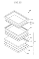
- FIG. 13 is an exploded perspective view of a liquid crystal display device using the light source module according to the present invention.
- the LCD device 400 of the present invention may include a top cover 310, a liquid crystal (LC) panel 320 and a backlight unit 380.
- LC liquid crystal
- the top cover 310 is arranged on the LC panel 320, thereby protecting the LC Panel 320 from an external shock.
- the LC panel 320 may include an array substrate 321, a color filter substrate 323 disposed to face the array substrate 321, and a liquid crystal layer (not shown) interposed between the array substrate 321 and the color filter substrate 323.
- the backlight unit 380 may be disposed below the LC panel 320, thereby providing light to the LC panel 320.
- the backlight unit 380 may include a light source module 200, a light guiding plate 350, an optical sheet 340, a reflection sheet 360 and a bottom cover 370.
- the light source module 200 includes a plurality of LED packages 101, and a printed circuit board (PCB) 210 on which the LED packages 101 are mounted.
- the light source module 200 may have the same configuration as the light source module aforementioned with reference to FIG. 11 or FIG. 12 .
- the light source module 200 may be arranged on one or more sides of the light guiding plate 350, and may be accommodated into a side wall of the bottom cover 370.
- the light guiding plate 350 may be arranged so as to be adjacent to the light source module 200, and may guide light generated from the light source module 200 to the LC panel 320.
- the optical sheet 340 may be arranged above the light guiding plate 350 in plurality, and may provide light transmitted from the light guiding plate 350 to the LC panel 320 after increasing efficiency of the light.
- the optical sheet 340 may include a diffusion sheet, a prism sheet and a protection sheet.
- the reflection sheet 360 may be disposed below the light guiding plate 350, and may reflect light leaked to a lower side of the light guiding plate 350 to the light guiding plate 350.
- the bottom cover 370 may have a bottom surface and side walls, and may accommodate therein the reflection sheet 360, the light guiding plate 350, the light source module 200 and the optical sheet 340.
- the backlight unit 380 may further include a guide panel 330.
- the guide panel 330 may be disposed between the LC panel 320 and the optical sheet 340, and may support the LC panel 320 together with the bottom cover 370. Also, the backlight unit 380 may fix the light guiding plate 350, the optical sheet 340 and the reflection sheet 360 to the bottom cover 370.
Landscapes
- Physics & Mathematics (AREA)
- General Physics & Mathematics (AREA)
- Optics & Photonics (AREA)
- Engineering & Computer Science (AREA)
- Microelectronics & Electronic Packaging (AREA)
- Led Device Packages (AREA)
- Planar Illumination Modules (AREA)
- Fastening Of Light Sources Or Lamp Holders (AREA)
- Arrangement Of Elements, Cooling, Sealing, Or The Like Of Lighting Devices (AREA)
- Non-Portable Lighting Devices Or Systems Thereof (AREA)
- Liquid Crystal (AREA)
Abstract
Description
- This application claims the benefit of Korean Patent Application No.
10-2013-0145536, filed on November. 27, 2013 - The present disclosure relates to a light emitting diode package, and particularly, to a light emitting diode package capable of reducing a size of a light source module by forming an additional line therein, a light source module and a backlight unit including the same.
- Generally, a liquid crystal display (LCD) device has a small thickness, a light weight, and low power consumption. Owing to such advantages, the LCD device is applied to a large television, etc., as well as a monitor, a notebook computer and a portable phone. Such LCD device includes a liquid crystal (LC) panel configured to display an image using an optical transmittance of liquid crystal molecules, and a backlight unit disposed below the LC panel and providing light to the LC panel.
- The backlight unit includes a light source module configured to generate light to be provided to the LC panel. A light source of the light source module may include a Cold Cathode Fluorescent Lamp (CCFL), a Flat Fluorescent Lamp (FFL), a Light Emitting Diode (LED), etc.
- The LED has characteristics of high light-emitting efficiency, long lifespan and low power consumption. Due to such characteristics, the LED is used as a light source of the light source module of the backlight unit. The LED is fabricated in the form of packages in which light emitting chips have been mounted, and is used as a light source of the light source module.
-
FIG. 1A is a schematic view illustrating a configuration of a light emitting diode (LED) package in accordance with the conventional art, andFIG. 1B is a sectional view taken along line I-I' inFIG. 1A . - Referring to
FIGS. 1A and 1B , theconventional LED package 1 includes alead frame 6 composed of two leads separated from each other, i.e., ananode lead 6a and acathode lead 6b; and aLED chip 4 mounted on one surface of thelead frame 6. - The
LED chip 4 is connected to theanode lead 6a and thecathode lead 6b of thelead frame 6, by awire 5 formed of gold (Au), silver (Ag), etc. - The
lead frame 6, theLED chip 4 and thewire 5 are enclosed by thecase 2 formed of opaque resin, etc. Part of theanode lead 6a and thecathode lead 6b of thelead frame 6 is exposed to outside so as to be mounted on a printed circuit board (not shown). - The
LED chip 4 enclosed by thecase 2 is covered by asealant 3 formed of transparent resin. -
FIG. 2 is a view schematically illustrating a light source module in accordance with the conventional art. - Referring to
FIG. 2 , a plurality ofLED packages 1 are mounted on a printedcircuit board 11, to thus constitute alight source module 10. - The plurality of
LED packages 1 are implemented in the form of groups, which are called chains. In the conventionallight source module 10, an odd-numberedLED package 1 and an even-numberedLED package 1 among the plurality ofLED packages 1 mounted on the printedcircuit board 11 are arranged in groups with two chain structures. - That is, the
light source module 10 has a plurality ofLED packages 1 mounted on the printedcircuit board 11 in groups with a first chain structure and a second chain structure. Each group is connected to lines formed at the printedcircuit board 11, i.e.,power supply lines connection lines - The first chain structure is composed of a
first LED package 1 connected to the firstpower supply line 13a of the printedcircuit board 11, athird LED package 1 connected to thefirst LED package 1 by thefirst connection line 14a, and afifth LED package 1. - The second chain structure is composed of a
second LED package 1 connected to the secondpower supply line 13b of the printedcircuit board 11, and afourth LED package 1 connected to thesecond LED package 1 by thesecond connection line 14b. - That is, the plurality of
LED packages 1 having the first chain structure, and the plurality ofLED packages 1 having the second chain structure are mounted on the printedcircuit board 11 so that electrodes thereof can alternate each other in polarity. For instance, thefirst LED package 1 having the first chain structure has electrodes (+), (-), and thethird LED package 1 connected to thefirst LED package 1 through thefirst connection line 14a has electrodes (-), (+). Further, thefifth LED package 1 connected to thethird LED package 1 through thefirst connection line 14a has electrodes (+), (-). Under such configuration, the plurality ofLED packages 1 having the first chain structure are connected to one another in serial. - The second chain structure is implemented in the same manner as the first chain structure. The first chain structure and the second chain structure are implemented in parallel.
- In the conventional
light source module 10, as the number of chain structures of theLED packages 1 is increased, a width (D) of the printedcircuit board 11 is increased. - For instance, in order to connect the plurality of
LED packages 1 having the second chain structure to one another, in a state where the plurality ofLED packages 1 having the first chain structure have been connected to one another through thefirst connection line 14a, thesecond connection line 14b should be formed at an upper end or a lower end of theLED package 1 having the first chain structure. Under such configuration, the width (D) of the printedcircuit board 11 is increased. - Further, as the number of the chain structures of the
LED packages 1 is increased, the printedcircuit board 11 of thelight source module 10 has a multi-layered structure. Accordingly, lines are formed even on a rear surface of the printedcircuit board 11. Lines formed on a front surface of the printedcircuit board 11 are connected to lines formed on a rear surface of the printedcircuit board 11, throughholes 15. As the number of chain structures is increased, the number of lines formed on the rear surface of the printedcircuit board 11, and the length of the lines are increased. - The
light source module 10 is accommodated in a side wall of an accommodating container(not shown) of the LCD device. As the LCD device becomes slim, the printedcircuit board 11 of thelight source module 10 has a limited width. - That is, in the conventional
light source module 10, as the number of chain structures of theLED package 1 is increased, the width (D) of the printedcircuit board 11 is increased. To solve such problem, the printedcircuit board 11 having a multi-layered structure is used. However, in this case, production cost of thelight source module 10 is increased. - Therefore, an aspect of the detailed description is to provide a light emitting diode package capable of reducing a width of a printed circuit board of a light source module, by forming a line therein, a light source module and a backlight unit including the same.
- To achieve these and other advantages and in accordance with the purpose of this specification, as embodied and broadly described herein, there is provided a light emitting diode (LED) package, comprising: a light emitting diode chip configured to generate light; a case configured to accommodate therein the light emitting diode chip; lead frames spaced from each other in the case, and having an anode lead and a cathode lead electrically-connected to the light emitting diode chip; and at least one dummy lead frame spaced from the lead frames in an insulated state to form a line.
- In one or more embodiments, the at least one dummy lead frame comprises at least two leads spaced from each other and electrically connected to each other in the case.
- In one or more embodiments, the dummy lead frame comprises: a first dummy lead spaced from the anode lead; and a second dummy lead spaced from the cathode lead, and connected to the first dummy lead in the case through a wire.
- In one or more embodiments, one end of the anode lead and one end of the cathode lead are exposed from two sides of the case, wherein one end of the first dummy lead is exposed from one side of the case to thus be spaced from the anode lead, and one end of the second dummy lead is exposed from another side of the case to thus be spaced from the cathode lead.
- In one or more embodiments, the dummy lead frame includes: a first dummy lead and a third dummy lead spaced from the anode lead; a second dummy lead spaced from the cathode lead, and connected to the first dummy lead in the case through a first wire; and a fourth dummy lead spaced from the cathode lead and the second dummy lead, and connected to the third dummy lead in the case through a second wire.
- In one or more embodiments, one end of the anode lead and one end of the cathode lead are exposed from two sides of the case, and wherein one end of the first dummy lead and one end of the third dummy lead are exposed from one side of the case, to thus face each other in a state where the anode lead is interposed therebetween, and wherein one end of the second dummy lead and one end of the fourth dummy lead are exposed from another side of the case, to thus face each other in a state where the cathode lead is interposed therebetween.
- In one or more embodiments, the dummy lead frame is extending from one side of the case to another side of the case through inside of the case, to thus be integrally formed, and wherein the dummy lead frame is spaced from the lead frame.
- In one or more embodiments, the dummy lead frame is extending from one side of the case to another side of the case through an outer surface of the case, to thus be integrally formed.
- In another aspect of the invention, there is provided a light source module, comprising: a printed circuit board; and a plurality of light emitting diode packages according to one or more embodiments described herein that are mounted sequentially arranged on the printed circuit board, having a first chain structure and a second chain structure, wherein an output of one light emitting diode package having the first chain structure is connected to another light emitting diode package having the first chain structure, through the dummy lead frame of an adjacent light emitting diode package having the second chain structure.
- In one or more embodiments, an output of a first light emitting diode package having the first chain structure is connected to a third light emitting diode package having the first chain structure, through the dummy lead frame of a second light emitting diode package having the second chain structure.
- In one or more embodiments, an output of a second light emitting diode package having the second chain structure is connected to a fourth light emitting diode package having the second chain structure, through the dummy lead frame of a third light emitting diode package having the first chain structure.
- In one or more embodiments, the light source module further comprises: a first connection line formed on the printed circuit board, and configured to connect an output of the plurality of light emitting diode packages having the first chain structure, to the dummy lead frame of the plurality of light emitting diode packages having the second chain structure; and a second connection line formed on the printed circuit board, and configured to connect an output of the plurality of light emitting diode packages having the second chain structure, to the dummy lead frame of the plurality of light emitting diode packages having the first chain structure.
- In one or more embodiments, the plurality of light emitting diode packages having the respective chain structures are arranged on the printed circuit board, such that electrodes thereof alternate each other in polarity.
- In another aspect of the invention, there is provided a light source module, comprising: a printed circuit board; and a plurality of light emitting diode packages according to one or more embodiments described herein that are mounted sequentially arranged on the printed circuit board, having a first chain structure, a second chain structure and a third chain structure, wherein an output of one light emitting diode package having the first chain structure is connected to another light emitting diode package having the first chain structure, through the dummy lead frame of an adjacent light emitting diode package having the second chain structure and the dummy lead frame of the light emitting diode package having the third chain structure.
- In another aspect of the invention, there is provided a backlight unit, comprising: a light source module according to one or more embodiments described herein; a light guiding plate arranged at one side of the light source module, and configured to guide light generated from the light source module; and an accommodation container configured to accommodate therein the light source module and the light guiding plate.
- In another aspect of the invention, there is provided a light emitting diode package, comprising: a light emitting diode chip configured to generate light; a case configured to accommodate therein the light emitting diode chip; lead frames spaced from each other in the case, and having an anode lead and a cathode lead electrically-connected to the light emitting diode chip; and at least one dummy lead frame spaced from the lead frames in an insulated state, and connected to each other in the case to form a line.
- To achieve these and other advantages and in accordance with the purpose of this specification, as embodied and broadly described herein, there is also provided a light source module, comprising: a printed circuit board; and a plurality of light emitting diode packages are mounted sequentially arranged on the printed circuit board, having a first chain structure and a second chain structure, wherein each of the plurality of light emitting diode packages including light emitting diode chip configured to generate light, a case configured to accommodate therein the light emitting diode chip, lead frames spaced from each other in the case, and having an anode lead and a cathode lead electrically-connected to the light emitting diode chip, and at least one dummy lead frame spaced from the lead frames in an insulated state, and connected to each other in the case to form a line.
- An output of one light emitting diode package having the first chain structure may be connected to another light emitting diode package having the first chain structure, through the dummy lead frame of an adjacent light emitting diode package having the second chain structure.
- To achieve these and other advantages and in accordance with the purpose of this specification, as embodied and broadly described herein, there is still also provided a backlight unit, comprising: a light source module; a light guiding plate arranged at one side of the light source module, and configured to guide light generated from the light source module; and an accommodation container configured to accommodate therein the light source module and the light guiding plate.
- The LED package, the light source module and the backlight unit including the same according to the present invention can have the following advantages.
- The plurality of LED packages can be mounted on the PCB without interference therebetween, by using at least one line formed therein. This can reduce a width of the PCB of the light source module, and reduce production cost of the light source module.
- Further scope of applicability of the present application will become more apparent from the detailed description given hereinafter. However, it should be understood that the detailed description and specific examples, while indicating preferred embodiments of the disclosure, are given by way of illustration only, since various changes and modifications within the spirit and scope of the disclosure will become apparent to those skilled in the art from the detailed description.
- The accompanying drawings, which are included to provide a further understanding of the disclosure and are incorporated in and constitute a part of this specification, illustrate exemplary embodiments and together with the description serve to explain the principles of the disclosure.
- In the drawings:
-
FIG. 1A is a schematic view illustrating a configuration of a light emitting diode (LED) package in accordance with the conventional art; -
FIG. 1 B is a sectional view taken along line I-I' inFIG. 1A ; -
FIG. 2 is a view schematically illustrating a light source module in accordance with the conventional art; -
FIG. 3 is a view schematically illustrating a configuration of a light emitting diode (LED) package according to a first embodiment of the present invention; -
FIG. 4 is a perspective view of the LED package ofFIG. 3 ; -
FIG. 5 is a view schematically illustrating a configuration of a light emitting diode (LED) package according to a second embodiment of the present invention; -
FIG. 6 is a perspective view of the LED package ofFIG. 5 ; -
FIG. 7 is a view schematically illustrating a configuration of a light emitting diode (LED) package according to a third embodiment of the resent invention; -
FIG. 8 is a perspective view of the LED package ofFIG. 7 ; -
FIG. 9 is a view schematically illustrating a configuration of a light emitting diode (LED) package according to a fourth embodiment of the resent invention; -
FIG. 10 is a perspective view of the LED package ofFIG. 9 ; -
FIG. 11 is a view schematically illustrating part of a light source module according to a first embodiment of the present invention; -
FIG. 12 is a view schematically illustrating part of a light source module according to a second embodiment of the present invention; and -
FIG. 13 is an exploded perspective view of a liquid crystal display device using a light source module according to the present invention. - Description will now be given in detail of the exemplary embodiments, with reference to the accompanying drawings. For the sake of brief description with reference to the drawings, the same or equivalent components will be provided with the same reference numbers, and description thereof will not be repeated.
- Hereinafter, a light emitting diode (LED) package, a light source module and a backlight unit according to the present invention will be explained in more detail with reference to the attached drawings. In the present invention, a liquid crystal display (LCD) device will be explained for convenience. However, the present invention may be applicable not only to a LCD device, but also to various flat display devices using a backlight unit.
-
FIG. 3 is a view schematically illustrating a configuration of a light emitting diode (LED) package according to a first embodiment of the present invention, andFIG. 4 is a perspective view of the LED package ofFIG. 3 . - Referring to
FIGS. 3 and4 , theLED package 100 according to the first embodiment of the present invention may include acase 110, lead frames 131, 133, dummy lead frames 141, 143, and aLED chip 120. - The
case 110 may be formed to have a 'U'-shape such that an upper surface is open. Thecase 110 may have an accommodation space for accommodating therein the lead frames 131, 133, the dummy lead frames 141, 143, and theLED chip 120. Thecase 110 may be formed of an insulating material such as polymer or ceramic, in order to insulate and protect the components accommodated therein. - A sealant (not shown), formed of a transparent resin, etc. in order to diffuse light generated from the
LED chip 120, may be filled in thecase 110. A reflecting material (not shown) may be coated on an inner side surface of thecase 110. - The lead frames 131, 133 may include an
anode lead 131 and acathode lead 133. Theanode lead 131 and thecathode lead 133 may be arranged at two sides of thecase 110, so as to correspond to each other. Theanode lead 131 and thecathode lead 133 may be electrically-insulated from each other in thecase 110, in a spaced state from each other. - One end of each of the
anode lead 131 and thecathode lead 133 may be exposed to outside of thecase 110. For instance, one end of theanode lead 131 may be exposed to outside from one side wall of thecase 110, and one end of thecathode lead 133 may be exposed to outside from another side wall of thecase 110. - The
LED chip 120 may be mounted on theanode lead 131 in thecase 110. TheLED chip 120 may be mounted on theanode lead 131 in a die-bonding manner by conductive epoxy. However, the present invention is not limited to this. In some cases, theLED chip 120 may be mounted on thecathode lead 133. - The
LED chip 120 may be electrically-connected to each of theanode lead 131 and thecathode lead 133, through afirst wire 135. For instance, an n-type electrode of theLED chip 120, i.e., an anode terminal may be connected to theanode lead 131 through thefirst wire 135. A p-type electrode of theLED chip 120, i.e., a cathode terminal may be connected to thecathode lead 133 through thefirst wire 135. - Although not shown, the
LED chip 120 may be composed of an n-type semiconductor layer, a p-type semiconductor layer, a light emitting layer formed between the two semiconductor layers, an n-type electrode connected to the n-type semiconductor layer, and a p-type electrode connected to the p-type semiconductor layer. - More specifically, the
LED chip 120 may be a GaN or GaN/AlGaN-based n-type semiconductor layer implemented as n-type semiconductor impurities have been doped on a substrate (not shown) formed of a transparent material such as sapphire, gallium nitride (GaN) and silicon carbide (SiC). The n-type semiconductor impurities may be silicon (Si), germanium (Ge) or tin (Sn). - A light emitting layer may be formed on the n-type semiconductor layer. The light emitting layer may be formed of a GaN-based material, and may have a single quantum well (SQW) structure or a multi quantum well (MQW) structure.
- A GaN or GaN/AlGaN-based p-type semiconductor layer, implemented as p-type semiconductor impurities have been doped on a substrate, may be formed on an activation layer. The p-type semiconductor impurities may be magnesium (Mg).
- The p-type semiconductor layer and the light emitting layer may be etched so that the n-type semiconductor layer can be partially exposed to outside. The n-type electrode may be formed on the n-type semiconductor layer exposed to outside by such etching. The p-type electrode may be formed on the p-type semiconductor layer having not been etched.
- Once an electric field is applied to the
LED chip 120 from outside through the n-type electrode and the p-type electrode, an electron and a hole may be provided to the light emitting layer from the n-type semiconductor layer and the p-type semiconductor layer. While the electron and the hole are re-coupled to each other at the light emitting layer, energy is generated. The energy may be converted into light, and the generated light may be emitted to outside. - The dummy lead frames 141, 143 may be spaced from the lead frames 131, 133, and may be electrically-insulated from each other. The dummy lead frames 141, 143 may include a
first dummy lead 141 and asecond dummy lead 143. - The
first dummy lead 141 may be disposed at one side of thecase 110, with a distance from theanode lead 131. The second dummy lead 142 may be disposed at another side of thecase 110, with a distance from thecathode lead 133. Thefirst dummy lead 141 and thesecond dummy lead 143 may be electrically-insulated from each other, in a spaced state from each other in thecase 110. - One end of each of the
first dummy lead 141 and thesecond dummy lead 143 may be exposed to outside of thecase 110. For instance, one end of thefirst dummy lead 141 may be exposed to outside from one side wall of thecase 110, and one end of thesecond dummy lead 143 may be exposed to outside from another side wall of thecase 110. The exposed end of thefirst dummy lead 141 and the exposed end of thesecond dummy lead 143 may correspond to each other at two sides of thecase 110. - The
first dummy lead 141 and thesecond dummy lead 143 may be electrically-connected to each other in thecase 110, through asecond wire 145. More specifically, thefirst dummy lead 141 and thesecond dummy lead 143 are spaced from the lead frames 131, 133 in an insulated state from each other, and are connected to each other by thesecond wire 145. Accordingly, thefirst dummy lead 141 and thesecond dummy lead 143 may be formed as a single line in theLED package 100. - The
LED package 100 according to the first embodiment of the present invention is provided therein with the dummy lead frames 141, 143 serving as additional lines. Accordingly, in a case where a plurality ofLED packages 100 are mounted on a printed circuit board (PCB) of a light source module to be explained later, the number of lines formed on the PCB, or the length of the line can be reduced. -
FIG. 5 is a view schematically illustrating a configuration of a light emitting diode (LED) package according to a second embodiment of the present invention, andFIG. 6 is a perspective view of the LED package ofFIG. 5 . - Referring to
FIGS. 5 and6 , theLED package 101 according to the second embodiment may include acase 110, lead frames 131, 133, first dummy lead frames 141, 143, second dummy lead frames 151, 153 and aLED chip 120. - The
case 110 has an open upper surface, and accommodates therein the lead frames 131, 133, the first dummy lead frames 141, 143, the second dummy lead frames 151, 153 and theLED chip 120. A sealant may be filled in thecase 110, and a reflecting material may be coated on an inner side surface of thecase 110. - The lead frames 131, 133 may include an
anode lead 131 and acathode lead 133. Theanode lead 131 and thecathode lead 133 are arranged at two sides of thecase 110 in correspondence to each other, and may be electrically-insulated from each other in a spaced state from each other in thecase 110. One end of theanode lead 131 may be exposed to outside from one side wall of thecase 110, and one end of thecathode lead 133 may be exposed to outside from another side wall of thecase 110. - The
LED chip 120 may be mounted on theanode lead 131 in thecase 110. TheLED chip 120 may be electrically-connected to theanode lead 131 and thecathode lead 133 through thefirst wire 135. An anode terminal of theLED chip 120 may be connected to theanode lead 131 through thefirst wire 135, and a cathode terminal of theLED chip 120 may be connected to thecathode lead 133 through thefirst wire 135. - Each of the first dummy lead frames 141, 143, and the second dummy lead frames 151, 153 may be spaced from the lead frames 131, 133, and may be electrically-insulated from each other. The first dummy lead frames 141, 143 may include a
first dummy lead 141 and asecond dummy lead 143. The second dummy lead frames 151, 153 may include athird dummy lead 151 and afourth dummy lead 153. - The
first dummy lead 141 may be spaced from theanode lead 131 at one side of thecase 110. Thesecond dummy lead 143 may be spaced from thecathode lead 133 at another side of thecase 110. Thefirst dummy lead 141 and thesecond dummy lead 143 may be spaced from each other to thus be electrically-insulated from each other in thecase 110. - The
third dummy lead 151 may be spaced from theanode lead 131 and thefirst dummy lead 141 at one side of thecase 110. Thefourth dummy lead 153 may be spaced from thecathode lead 133 and thesecond dummy lead 143 at another side of thecase 110. Thethird dummy lead 151 and thefourth dummy lead 153 may be spaced from each other to thus be electrically-insulated from each other in thecase 110. - That is, the
third dummy lead 151 may be arranged to face thefirst dummy lead 141 at one side of thecase 110, in a state where theanode lead 131 is interposed between thefirst dummy lead 141 and thethird dummy lead 151. Thefourth dummy lead 153 may be arranged to face thesecond dummy lead 143 at another side of thecase 110, in a state where thecathode lead 133 is interposed between thesecond dummy lead 143 and thefourth dummy lead 153. - One end of the
first dummy lead 141 may be exposed to outside of thecase 110, and one end of thesecond dummy lead 143 may be exposed to outside of thecase 110. The exposed end of thefirst dummy lead 141 and the exposed end of thesecond dummy lead 143 may correspond to each other at two sides of thecase 110. - One end of the
third dummy lead 151 may be exposed to outside of thecase 110, and one end of thefourth dummy lead 153 may be exposed to outside of thecase 110. The exposed end of thethird dummy lead 151 and the exposed end of thefourth dummy lead 153 may correspond to each other at two sides of thecase 110. - The exposed
first dummy lead 141 and the exposedthird dummy lead 151 may face each other at one side of thecase 110, in a state where the exposedanode lead 131 is interposed therebetween. The exposedsecond dummy lead 143 and the exposedfourth dummy lead 153 may face each other at another side of thecase 110, in a state where the exposedcathode lead 133 is interposed therebetween. - The
first dummy lead 141 and thesecond dummy lead 143 may be electrically-connected to each other in thecase 110 through thesecond wire 145, and thethird dummy lead 151 and thefourth dummy lead 153 may be electrically-connected to each other in thecase 110 through athird line 155. - That is, the
first dummy lead 141 and thesecond dummy lead 143 may be connected to each other in thecase 110 through thesecond wire 145, thereby forming one single line. Thethird dummy lead 151 and thefourth dummy lead 153 may be connected to each other in thecase 110 through thethird line 155, thereby forming another single line. - The
LED package 101 according to the second embodiment of the present invention is provided therein with two types of dummy lead frames serving as additional lines, i. e., the first dummy lead frames 141, 143 and the second dummy lead frames 151, 153. As a result, in a case where theLED package 100 is mounted on a printed circuit board (PCB), the number of lines formed on the PCB, or the length of the line can be reduced. -
FIG. 7 is a view schematically illustrating a configuration of a light emitting diode (LED) package according to a third embodiment of the resent invention, andFIG. 8 is a perspective view of the LED package ofFIG. 7 . - The
LED package 102 according to the third embodiment is the same as theLED package 100 aforementioned with reference toFIGS. 3 and4 , except that adummy lead frame 160 is integrally formed with theLED package 102. Accordingly, detailed explanations on the same components will be omitted. - Referring to
FIGS. 7 and8 , theLED package 102 according to the third embodiment may include acase 110, lead frames 131, 133, adummy lead frame 160 and aLED chip 120. - The
case 110 has an open upper surface, and accommodates therein the lead frames 131, 133, thedummy lead frame 160 and theLED chip 120. A sealant may be filled in thecase 110, and a reflecting material may be coated on an inner side surface of thecase 110. - The lead frames 131, 133 may include an
anode lead 131 and acathode lead 133. Theanode lead 131 and thecathode lead 133 may be arranged at two sides of thecase 110, so as to correspond to each other. Theanode lead 131 and thecathode lead 133 may be electrically-insulated from each other in thecase 110, in a spaced state from each other. One end of theanode lead 131 may be exposed to outside from one side wall of thecase 110, and one end of thecathode lead 133 may be exposed to outside from another side wall of thecase 110. - The
LED chip 120 may be mounted on theanode lead 131 in thecase 110. TheLED chip 120 may be electrically-connected to theanode lead 131 and thecathode lead 133 through thefirst wire 135. An anode terminal of theLED chip 120 may be connected to theanode lead 131 through thefirst wire 135, and a cathode terminal of theLED chip 120 may be connected to thecathode lead 133 through thefirst wire 135. - The
dummy lead frame 160 may be extending from one side of thecase 110 to another side of thecase 110 through inside of thecase 110, thereby being integrally formed. Thedummy lead frame 160 may be spaced from the lead frames 131, 133, and may be insulated from the lead frames 131, 133. - One side of the
dummy lead frame 160 may be exposed to outside from one side wall of thecase 110, and another side thereof may be exposed to outside from another side wall of thecase 110. - Said one exposed side of the
dummy frame 160 may be spaced from theanode lead 131 at one side of thecase 110. Said another exposed side of thedummy frame 160 may be spaced from thecathode lead 133 at another side of thecase 110. - Said one exposed side of the
dummy frame 160 and said another exposed side of thedummy frame 160 may be may correspond to each other at two sides of thecase 110. - That is, the
LED package 102 according to the third embodiment is provided therein with thedummy lead frame 160 serving as an additional line. This can reduce the number of lines of a printed circuit board (PCB) on which theLED package 102 is to be mounted, or the length of the line. - In the third embodiment, the
LED package 102 is provided therein with onedummy lead frame 160, thereby forming a line. However, the present invention is not limited to this. For instance, theLED package 102 may be provided therein with two dummy lead frames 160, thereby forming two lines. The two dummy lead frames 160 may be spaced from each other in an insulated state from each other. And the two dummy lead frames 160 may be arranged to face each other at two sides of thecase 110, based on theanode lead 131 and thecathode lead 133. -
FIG. 9 is a view schematically illustrating a configuration of a light emitting diode (LED) package according to a fourth embodiment of the resent invention, andFIG. 10 is a perspective view of the LED package ofFIG. 9 . - The
LED package 103 according to the fourth embodiment is the same as theLED package 100 aforementioned with reference toFIGS. 3 and4 , except that adummy lead frame 170 is formed on an outer surface of theLED package 103. Accordingly, detailed explanations on the same components will be omitted. - Referring to
FIGS. 9 and10 , theLED package 103 according to the fourth embodiment may include acase 110, lead frames 131, 133, adummy lead frame 170 and aLED chip 120. - The
case 110 has an open upper surface, and accommodates therein the lead frames 131, 133 and theLED chip 120. A sealant may be filled in thecase 110, and a reflecting material may be coated on an inner side surface of thecase 110. - The lead frames 131, 133 may include an
anode lead 131 and acathode lead 133. Theanode lead 131 and thecathode lead 133 may be arranged at two sides of thecase 110, so as to correspond to each other. Theanode lead 131 and thecathode lead 133 may be electrically-insulated from each other in thecase 110, in a spaced state from each other. One end of theanode lead 131 may be exposed to outside from one side wall of thecase 110, and one end of thecathode lead 133 may be exposed to outside from another side wall of thecase 110. - The
LED chip 120 may be mounted on theanode lead 131 in thecase 110. TheLED chip 120 may be electrically-connected to theanode lead 131 and thecathode lead 133 through thefirst wire 135. An anode terminal of theLED chip 120 may be connected to theanode lead 131 through thefirst wire 135, and a cathode terminal of theLED chip 120 may be connected to thecathode lead 133 through thefirst wire 135. - The
dummy lead frame 170 may be extending from one side of thecase 110 to another side of thecase 110, along an outer surface of thecase 110, thereby being integrally formed. One side of thedummy lead frame 170 may be spaced from theanode lead 131 at one side of thecase 110. Another side of thedummy lead frame 170 may be spaced from thecathode lead 133 at another side of thecase 110. - One side and another side of the
dummy lead frame 170 may correspond to each other at two sides of thecase 110. - That is, the
LED package 103 according to the fourth embodiment is provided with thedummy lead frame 170 serving as an additional line, along an outer surface of thecase 110. This can reduce the number of lines of a printed circuit board (PCB) on which theLED package 103 is to be mounted, or the length of the line. - In the fourth embodiment, the
LED package 103 is provided with onedummy lead frame 170 along one outer surface of thecase 110, thereby forming a line. However, the present invention is not limited to this. For instance, theLED package 103 may be provided with two dummy lead frames 170 along two outer surfaces of thecase 110, thereby forming two lines. -
FIG. 11 is a view schematically illustrating part of a light source module according to a first embodiment of the present invention. - In this embodiment, a
light source module 200 using theLED package 101 aforementioned with reference toFIGS. 5 and6 will be explained for convenience. However, the various LED packages according to the aforementioned embodiments may be applied to thelight source module 200. - Referring to
FIG. 11 , thelight source module 200 according to the first embodiment may include a printed circuit board (PCB) 210, and a plurality of light emitting diode (LED) packages 101_a1 to 101_b2 mounted on thePCB 210. - A plurality of lines may be formed on the
PCB 210. For instance, afirst power line 211 and asecond power line 213, configured to supply operation power to the LED packages 101_a1 to 101_b2, respectively, may be formed on thePCB 210. Afirst connection line 221 and asecond connection line 223, configured to connect the LED packages 101_a1 to 101_b2 to each other, may be formed on thePCB 210. - The
first connection line 221 serves to connect a LED package 101_a1, 101_a2 having a first chain structure, with an adjacent LED package 101_b1, 101_b2 having a second chain structure. Thesecond connection line 223 serves to connect aLED package 101 b1, 101_b2 having a second chain structure, with an adjacent LED package 101_a1, 101_a2 having a first chain structure. - As aforementioned with reference to
FIGS. 5 and6 , the LED packages 101_a1 to 101_b2 are provided therein with first dummy lead frames 141, 143 and second dummy lead frames 151, 153 serving as two lines by being separately formed from the lead frames 131, 133. - The plurality of LED packages 101_a1 to 101_b2 may be mounted on the
PCB 210 in an inline form. The plurality of LED packages 101_a1 to 101_b2 may have chain structures as a predetermined number of LED packages are formed in groups. - For instance, odd-numbered LED packages 101_a1, 101_a2, among the plurality of LED packages 101_a1 to 101_b2 mounted on the
PCB 210, have a first chain structure as one group. - Even-numbered LED packages 101_b1, 101_b2, among the plurality of LED packages 101_a1 to 101_b2 mounted on the
PCB 210, have a second chain structure as another group. - Under such configuration, the plurality of LED packages 101_a1, 101_a2 having the first chain structure, and the plurality of LED packages 101_b1, 101_b2 having the second chain structure may be sequentially mounted on the
PCB 210. For instance, the plurality of LED packages 101_a1 to 101_b2 may be mounted on thePCB 210, in order of the first chain structure and the second chain structure. - The first chain structure may be implemented by the first LED package 101_a1 connected to the
first power line 211 of thePCB 210, and the third LED package 101_a2 connected to the first LED package 101_a1 through thefirst connection line 221. - The second chain structure may be implemented by the second LED package 101_b1 connected to the
second power line 213 of thePCB 210, and the fourth LED package 101_b2 connected to the second LED package 101_b1 through thesecond connection line 223. - The first LED package 101_a1 and the third LED package 101_a2 having the first chain structure may be mounted on the
PCB 210 so that electrodes thereof can alternate each other in polarity. For instance, the first LED package 101_a1 of the first chain structure may be mounted on thePCB 210 so that electrodes thereof can be arranged in the form of (+), (-). On the contrary, the third LED package 101_a2 having the first chain structure may be mounted on thePCB 210 so that electrodes thereof can be arranged in the form of (-), (+). Likewise, the plurality of LED packages 101_b1, 101_b2 of the second chain structure may be mounted on thePCB 210 so that electrodes thereof can alternate each other in polarity. - Hereinafter, a method for connecting the plurality of LED packages 101_a1 to 101_b2 having the respective structures in the
light source module 200 will be explained in more detail. - Firstly, the
anode lead 131 of the first LED package 101_a1 having the first chain structure is connected to thefirst power line 211, thereby receiving operating power from outside. An output from the first LED package 101_a1 is provided to athird dummy lead 151 of the second LED package 101_b1 having the second chain structure, through thecathode lead 133 of the first LED package 101_a1 and thefirst connection line 221. - Then the output from the first LED package 101_a1 is provided to the
cathode lead 133 of the third LED package 101_a2 having the first chain structure, through thethird dummy lead 151 and thefourth dummy lead 153 connected to each other in the second LED package 101_b1, and through thesecond connection line 223. - That is, the output from the first LED package 101_a1 having the first chain structure may be provided to the
cathode lead 133 of the third LED package 101_a2, through the second dummy lead frames 151, 153 of the second LED package 101_b1 having the second chain structure. - The
anode lead 131 of the second LED package 101_b1 having the second chain structure is connected to thesecond power line 213, thereby receiving operating power from outside. An output from the second LED package 101_b1 is provided to afirst dummy lead 141 of the third LED package 101_a2 having the first chain structure, through thecathode lead 133 of the second LED package 101_b1 and thesecond connection line 223. - Then the output from the second LED package 101_b1 is provided to the
cathode lead 133 of the fourth LED package 101_b2 having the second chain structure, through thefirst dummy lead 141 and thesecond dummy lead 143 connected to each other in the third LED package 101_a2, and through thefirst connection line 221. - That is, the output from the second LED package 101_b1 having the second chain structure may be provided to the
cathode lead 133 of the fourth LED package 101_b2, through the first dummy lead frames 141, 143 of the third LED package 101_a2 having the first chain structure. - As aforementioned, in the
light source module 200 of the present invention, the plurality of LED packages 101_a1 to 101_b2 having different chain structures are connected to each other by using a line formed in an adjacent LED package, i.e., a dummy lead frame. This can allow a width (d1) of the printed circuit board (PCB) 210 to be reduced. - Under such configuration, the
light source module 200 according to the first embodiment of the present invention can have the width (d1) of thePCB 210 more reduced than that of the conventional light source module. Accordingly, production cost of thelight source module 200 according to the first embodiment of the present invention can be reduced. - As the first LED package 101_a1 between the plurality of LED packages 101_a1 to 101_b2 mounted on the
PCB 210 of thelight source module 200, the conventional LED package aforementioned with reference toFIGS. 1A and 1B may be used. -
FIG. 12 is a view schematically illustrating part of a light source module according to a second embodiment of the present invention. - In the
light source module 201 according to the second embodiment, a plurality of LED packages 101_a1 to 101_c2 may be mounted on aPCB 210 with 3 chain structures. - More specifically, a first LED package 101_a1 and a fourth LED package 101_a2 among the plurality of LED packages 101_a1 to 101_c2 mounted on the
PCB 210, may have a first chain structure as one group. - A second LED package 101_b1 and a fifth LED package 101_b2 among the plurality of LED packages 101_a1 to 101_c2 mounted on the
PCB 210, may have a second chain structure as another group. - A third LED package 101_c1 and a sixth LED package 101_c2 among the plurality of LED packages 101_a1 to 101_c2 mounted on the
PCB 210, may have a third chain structure as still another group. - Under such configuration, the plurality of LED packages 101_a1, 101_a2 having the first chain structure, the plurality of LED packages 101_b1, 101_b2 having the second chain structure, and the plurality of LED packages 101_c1, 101_c2 having the third chain structure may be sequentially mounted on the
PCB 210. For instance, the plurality of LED packages 101_a1 to 101_c2 may be mounted on thePCB 210, in order of the first chain structure, the second structure and the third chain structure. - The plurality of LED packages 101_a1 to 101_c2 having different chain structures may be mounted on the
PCB 210 so that electrodes thereof can alternate each other in polarity. More specifically, the first LED package 101_a1 and the fourth LED package 101_a2, the second LED package 101_b1 and the fifth LED package 101_b2, and the third LED package 101_c1 and the sixth LED package 101_c2 may be mounted on thePCB 210 so that electrodes thereof can alternate each other in polarity. - A plurality of lines may be formed on the
PCB 210. For instance, afirst power line 211, asecond power line 213 and athird power line 215 for supplying operation power to the plurality of LED packages 101_a1 to 101_c2 may be formed on thePCB 210. Also, afirst connection line 221, asecond connection line 223 and athird connection line 225 for connecting the plurality of LED packages 101_a1 to 101_c2 to one another may be formed on thePCB 210. - The
first connection line 221 serves to connect a LED package having a first chain structure, with an adjacent LED package having a second chain structure. Thesecond connection line 223 serves to connect a LED package having a second chain structure, with an adjacent LED package having a third chain structure. Thethird connection line 225 serves to connect a LED package having a third chain structure, with an adjacent LED package having a first chain structure. - Hereinafter, a method for connecting the plurality of LED packages 101_a1 to 101_c2 having the respective chain structures in the
light source module 201 will be explained in more detail. - Firstly, the
anode lead 131 of the first LED package 101_a1 having the first chain structure is connected to thefirst power line 211, thereby receiving operating power from outside. An output from the first LED package 101_a1 is provided to athird dummy lead 151 of the second LED package 101_b1 having the second chain structure, through thecathode lead 133 of the first LED package 101_a1 and thefirst connection line 221. - Then the output from the first LED package 101_a1, which has been provided to the second LED package 101_b1, is provided to the
third dummy lead 151 of the third LED package 101_c1 having the third chain structure, through thethird dummy lead 151 and thefourth dummy lead 153 connected to each other in the second LED package 101_b1, and through thesecond connection line 223. - Then the output from the first LED package 101_a1, which has been provided to the third LED package 101_c1, is provided to the
cathode lead 133 of the fourth LED package 101_a2 having the first chain structure, through thethird dummy lead 151 and thefourth dummy lead 153 connected to each other in the third LED package 101_c1, and through thethird connection line 225. - That is, the output from the first LED package 101_a1 having the first chain structure may be provided to the
cathode lead 133 of the fourth LED package 101_a2, through the second dummy lead frames 151, 153 of the second LED package 101_b1 having the second chain structure, and through the second dummy lead frames 151, 153 of the third LED package 101_c1 having the third chain structure. - The
anode lead 131 of the second LED package 101_b1 having the second chain structure is connected to thesecond power line 213, thereby receiving operating power from outside. An output from the second LED package 101_b1 is provided to afirst dummy lead 141 of the third LED package 101_c1 having the third chain structure, through thecathode lead 133 of the second LED package 101_b1 and thesecond connection line 223. - A
hole 230 is formed between thecathode lead 133 of the second LED package 101_b1 and thefirst dummy lead 141 of the third LED package 101_c1. Thesecond connection line 223 is formed on a rear surface of thePCB 210, thereby connecting thecathode lead 133 of the second LED package 101_b1 to thefirst dummy lead 141 of the third LED package 101_c1 through thehole 230. - An output from the second LED package 101_b1, which has been provided to the third LED package 101_c1, is provided to the
first dummy lead 141 of the fourth LED package 101_a2 having the first chain structure, through thefirst dummy lead 141 and thesecond dummy lead 143 connected to each other in the third LED package 101_c1, and through thethird connection line 225. - The output from the second LED package 101_b1, which has been provided to the fourth LED package 101_a2, is provided to the
cathode lead 133 of the fifth LED package 101_b2 having the second chain structure, through thefirst dummy lead 141 and thesecond dummy lead 143 connected to each other in the fourth LED package 101_a2, and through thefirst connection line 221. - That is, the output from the second LED package 101_b1 having the second chain structure may be provided to the
cathode lead 133 of the fifth LED package 101_b2, through the first dummy lead frames 141, 143 of the third LED package 101_c1 having the third chain structure, and through the first dummy lead frames 141, 143 of the fourth LED package 101_a2 having the first chain structure. - The
anode lead 131 of the third LED package 101_c1 having the third chain structure is connected to thethird power line 215, thereby receiving power from outside. An output from the third LED package 101_c1 is provided to thethird dummy lead 151 of the fourth LED package 101_a2 having the first chain structure, through thecathode lead 133 of the third LED package 101_c1 and thethird connection line 225. - The
hole 230 is formed between thecathode lead 133 of the third LED package 101_c1 and thethird dummy lead 151 of the fourth LED package 101_a2. Thethird connection line 225 is formed on a rear surface of thePCB 210, thereby connecting thecathode lead 133 of the third LED package 101_c1 to thethird dummy lead 151 of the fourth LED package 101_a2 through thehole 230. - The output from the third LED package 101_c1, which has been provided to the fourth LED package 101_a2, is provided to the
third dummy lead 151 of the fifth LED package 101_b2 having the second chain structure, through thethird dummy lead 151 and thefourth dummy lead 153 connected to each other in the fourth LED package 101_a2, and through thefirst connection line 221. - The output from the third LED package 101_c1, which has been provided to the fifth LED package 101_b2, is provided to the
cathode lead 133 of the sixth LED package 101_c2 having the third chain structure, through thethird dummy lead 151 and thefourth dummy lead 153 connected to each other in the fifth LED package 101_b2, and through thesecond connection line 223. - That is, the output from the third LED package 101_c1 having the third chain structure may be provided to the
cathode lead 133 of the sixth LED package 101_c2, through the second dummy lead frames 151, 153 of the fourth LED package 101_a2 having the first chain structure, and through the second dummy lead frames 151, 153 of the fifth LED package 101_b2 having the first chain structure. - As the first LED package 101_a1 among the plurality of LED packages 101_a1 to 101_c2 mounted on the
PCB 210 of thelight source module 201, the conventional LED package aforementioned with reference toFIGS. 1A and 1B may be used. - As aforementioned, in the
light source module 201 according to the second embodiment, the plurality of LED packages 101_a1 to 101_c2 having various chain structures are connected to each other (i.e., the first LED package 101_a1 and the fourth LED package 101_a2 are connected to each other) by using at least one dummy lead frame formed in the adjacent LED packages. This can allow a width (d2) of thePCB 210 to be reduced. - Under such configuration, the
light source module 201 according to the second embodiment of the present invention can have the width (d2) of thePCB 210 more reduced than that of the conventional light source module. Accordingly, production cost of thelight source module 201 according to the second embodiment of the present invention can be reduced. - In the
light source module 201 according to the second embodiment, thePCB 210 has a double-layered structure where theholes 230 have been formed. Theholes 230 are formed among the plurality of LED packages 101_a1 to 101_c2. As a result, a line, formed on a rear surface of thePCB 210 and connecting theholes 230 to each other, can have a shorter length than that in the conventional light source module. -
FIG. 13 is an exploded perspective view of a liquid crystal display device using the light source module according to the present invention. - Referring to
FIG. 13 , theLCD device 400 of the present invention may include atop cover 310, a liquid crystal (LC)panel 320 and abacklight unit 380. - The
top cover 310 is arranged on theLC panel 320, thereby protecting theLC Panel 320 from an external shock. A window, through which a display region of theLC panel 320 is exposed to outside, is formed at thetop cover 310. - The
LC panel 320 may include anarray substrate 321, acolor filter substrate 323 disposed to face thearray substrate 321, and a liquid crystal layer (not shown) interposed between thearray substrate 321 and thecolor filter substrate 323. - The
backlight unit 380 may be disposed below theLC panel 320, thereby providing light to theLC panel 320. - The
backlight unit 380 may include alight source module 200, alight guiding plate 350, anoptical sheet 340, areflection sheet 360 and abottom cover 370. - The
light source module 200 includes a plurality ofLED packages 101, and a printed circuit board (PCB) 210 on which the LED packages 101 are mounted. Thelight source module 200 may have the same configuration as the light source module aforementioned with reference toFIG. 11 orFIG. 12 . - The
light source module 200 may be arranged on one or more sides of thelight guiding plate 350, and may be accommodated into a side wall of thebottom cover 370. - The
light guiding plate 350 may be arranged so as to be adjacent to thelight source module 200, and may guide light generated from thelight source module 200 to theLC panel 320. - The
optical sheet 340 may be arranged above thelight guiding plate 350 in plurality, and may provide light transmitted from thelight guiding plate 350 to theLC panel 320 after increasing efficiency of the light. Theoptical sheet 340 may include a diffusion sheet, a prism sheet and a protection sheet. - The
reflection sheet 360 may be disposed below thelight guiding plate 350, and may reflect light leaked to a lower side of thelight guiding plate 350 to thelight guiding plate 350. - The
bottom cover 370 may have a bottom surface and side walls, and may accommodate therein thereflection sheet 360, thelight guiding plate 350, thelight source module 200 and theoptical sheet 340. - The
backlight unit 380 may further include aguide panel 330. Theguide panel 330 may be disposed between theLC panel 320 and theoptical sheet 340, and may support theLC panel 320 together with thebottom cover 370. Also, thebacklight unit 380 may fix thelight guiding plate 350, theoptical sheet 340 and thereflection sheet 360 to thebottom cover 370. - The foregoing embodiments and advantages are merely exemplary and are not to be considered as limiting the present disclosure. The present teachings can be readily applied to other types of apparatuses. This description is intended to be illustrative, and not to limit the scope of the claims. Many alternatives, modifications, and variations will be apparent to those skilled in the art. The features, structures, methods, and other characteristics of the exemplary embodiments described herein may be combined in various ways to obtain additional and/or alternative exemplary embodiments.
- As the present features may be embodied in several forms without departing from the characteristics thereof, it should also be understood that the above-described embodiments are not limited by any of the details of the foregoing description, unless otherwise specified, but rather should be considered broadly within its scope as defined in the appended claims, and therefore all changes and modifications that fall within the metes and bounds of the claims, or equivalents of such metes and bounds are therefore intended to be embraced by the appended claims.
Claims (15)
- A light emitting diode package, comprising:a light emitting diode chip configured to generate light;a case configured to accommodate therein the light emitting diode chip;lead frames spaced from each other in the case, and having an anode lead and a cathode lead electrically-connected to the light emitting diode chip; andat least one dummy lead frame spaced from the lead frames in an insulated state to form a line.
- The light emitting diode package of claim 1, wherein the at least one dummy lead frame comprises at least two leads spaced from each other and electrically connected to each other in the case.
- The light emitting diode package of claim 1, wherein the dummy lead frame comprises:a first dummy lead spaced from the anode lead; anda second dummy lead spaced from the cathode lead, and connected to the first dummy lead in the case through a wire.
- The light emitting diode package of claim 3, wherein one end of the anode lead and one end of the cathode lead are exposed from two sides of the case,
wherein one end of the first dummy lead is exposed from one side of the case to thus be spaced from the anode lead, and one end of the second dummy lead is exposed from another side of the case to thus be spaced from the cathode lead. - The light emitting diode package of claim 1, wherein the dummy lead frame includes:a first dummy lead and a third dummy lead spaced from the anode lead;a second dummy lead spaced from the cathode lead, and connected to the first dummy lead in the case through a first wire; anda fourth dummy lead spaced from the cathode lead and the second dummy lead, and connected to the third dummy lead in the case through a second wire.
- The light emitting diode package of claim 5, wherein one end of the anode lead and one end of the cathode lead are exposed from two sides of the case, and
wherein one end of the first dummy lead and one end of the third dummy lead are exposed from one side of the case, to thus face each other in a state where the anode lead is interposed therebetween, and
wherein one end of the second dummy lead and one end of the fourth dummy lead are exposed from another side of the case, to thus face each other in a state where the cathode lead is interposed therebetween. - The light emitting diode package of claim 1, wherein the dummy lead frame is extending from one side of the case to another side of the case through inside of the case, to thus be integrally formed, and
wherein the dummy lead frame is spaced from the lead frame. - The light emitting diode package of claim 1, wherein the dummy lead frame is extending from one side of the case to another side of the case through an outer surface of the case, to thus be integrally formed.
- A light source module, comprising:a printed circuit board; anda plurality of light emitting diode packages according to any one of claims 1 to 8 that are mounted sequentially arranged on the printed circuit board, having a first chain structure and a second chain structure,wherein an output of one light emitting diode package having the first chain structure is connected to another light emitting diode package having the first chain structure, through the dummy lead frame of an adjacent light emitting diode package having the second chain structure.
- The light source module of claim 9, wherein an output of a first light emitting diode package having the first chain structure is connected to a third light emitting diode package having the first chain structure, through the dummy lead frame of a second light emitting diode package having the second chain structure.
- The light source module of claim 9, wherein an output of a second light emitting diode package having the second chain structure is connected to a fourth light emitting diode package having the second chain structure, through the dummy lead frame of a third light emitting diode package having the first chain structure.
- The light source module of any one of claims 9 to 11, further comprising:a first connection line formed on the printed circuit board, and configured to connect an output of the plurality of light emitting diode packages having the first chain structure, to the dummy lead frame of the plurality of light emitting diode packages having the second chain structure; anda second connection line formed on the printed circuit board, and configured to connect an output of the plurality of light emitting diode packages having the second chain structure, to the dummy lead frame of the plurality of light emitting diode packages having the first chain structure.
- The light source module of any one of claims 9 to 12, wherein the plurality of light emitting diode packages having the respective chain structures are arranged on the printed circuit board, such that electrodes thereof alternate each other in polarity.
- A light source module, comprising:a printed circuit board; anda plurality of light emitting diode packages according to any one of claims 1 to 8 that are mounted sequentially arranged on the printed circuit board, having a first chain structure, a second chain structure and a third chain structure,wherein an output of one light emitting diode package having the first chain structure is connected to another light emitting diode package having the first chain structure, through the dummy lead frame of an adjacent light emitting diode package having the second chain structure and the dummy lead frame of the light emitting diode package having the third chain structure.
- A backlight unit, comprising:a light source module according to any one of claims 9 to 14;a light guiding plate arranged at one side of the light source module, and configured to guide light generated from the light source module; andan accommodation container configured to accommodate therein the light source module and the light guiding plate.
Applications Claiming Priority (1)
| Application Number | Priority Date | Filing Date | Title |
|---|---|---|---|
| KR1020130145536A KR101545926B1 (en) | 2013-11-27 | 2013-11-27 | Lighting module and backlight unit including the same |
Publications (2)
| Publication Number | Publication Date |
|---|---|
| EP2879194A1 true EP2879194A1 (en) | 2015-06-03 |
| EP2879194B1 EP2879194B1 (en) | 2019-08-28 |
Family
ID=50819595
Family Applications (1)
| Application Number | Title | Priority Date | Filing Date |
|---|---|---|---|
| EP14169951.2A Active EP2879194B1 (en) | 2013-11-27 | 2014-05-27 | Light source module and backlight unit including the same |
Country Status (5)
| Country | Link |
|---|---|
| US (1) | US9236534B2 (en) |
| EP (1) | EP2879194B1 (en) |
| JP (1) | JP6049672B2 (en) |
| KR (1) | KR101545926B1 (en) |
| CN (1) | CN104681701B (en) |
Families Citing this family (3)
| Publication number | Priority date | Publication date | Assignee | Title |
|---|---|---|---|---|
| JP6578739B2 (en) | 2015-05-21 | 2019-09-25 | スズキ株式会社 | Steering wheel suspension |
| EP3908781B1 (en) | 2019-01-09 | 2023-08-23 | Lumileds Holding B.V. | Lighting device for backlighting of display screen |
| CN111584701A (en) * | 2020-04-16 | 2020-08-25 | 慧明光电(深圳)有限公司 | Novel LED lamp bead packaging method |
Citations (3)
| Publication number | Priority date | Publication date | Assignee | Title |
|---|---|---|---|---|
| US20090224268A1 (en) * | 2008-03-10 | 2009-09-10 | Citizen Electronics Co., Ltd. | Light-emitting diode and lighting apparatus using the same |
| US20120163026A1 (en) * | 2010-12-22 | 2012-06-28 | Jeon Myoung-Ha | Light-emitting diode package, light source module having the same and backlight assembly having the same |
| US20130105851A1 (en) * | 2011-10-27 | 2013-05-02 | Seoul Semiconductor Co., Ltd. | Light emitting diode package and light emitting module comprising the same |
Family Cites Families (9)
| Publication number | Priority date | Publication date | Assignee | Title |
|---|---|---|---|---|
| KR0145841B1 (en) | 1995-06-30 | 1998-08-01 | 김광호 | Padless leadframe and plastic package using it |
| KR0169893B1 (en) | 1996-02-05 | 1999-01-15 | 김광호 | Power package with direct connection between dummy lead and heat sink |
| JP2001085599A (en) * | 1999-09-16 | 2001-03-30 | Toshiba Corp | Semiconductor device |
| KR100632256B1 (en) | 1999-11-12 | 2006-10-11 | 삼성전자주식회사 | Lead-on Chip Lead Frame with Dummy Leads |
| JP2001185578A (en) * | 1999-12-24 | 2001-07-06 | Toshiba Corp | Semiconductor device |
| KR200299491Y1 (en) * | 2002-09-02 | 2003-01-03 | 코리아옵토 주식회사 | A Surface mounting type light emitting diode |
| JP4129437B2 (en) | 2004-01-28 | 2008-08-06 | 日本板硝子株式会社 | Line lighting device |
| TWI485878B (en) | 2009-04-01 | 2015-05-21 | 光寶科技股份有限公司 | Method for forming a lens structure of a light-emitting diode and related structure |
| JP2012175054A (en) * | 2011-02-24 | 2012-09-10 | Citizen Electronics Co Ltd | Led package |
-
2013
- 2013-11-27 KR KR1020130145536A patent/KR101545926B1/en not_active Expired - Fee Related
-
2014
- 2014-05-14 US US14/277,237 patent/US9236534B2/en not_active Expired - Fee Related
- 2014-05-27 EP EP14169951.2A patent/EP2879194B1/en active Active
- 2014-06-09 CN CN201410253163.0A patent/CN104681701B/en not_active Expired - Fee Related
- 2014-10-31 JP JP2014222750A patent/JP6049672B2/en active Active
Patent Citations (3)
| Publication number | Priority date | Publication date | Assignee | Title |
|---|---|---|---|---|
| US20090224268A1 (en) * | 2008-03-10 | 2009-09-10 | Citizen Electronics Co., Ltd. | Light-emitting diode and lighting apparatus using the same |
| US20120163026A1 (en) * | 2010-12-22 | 2012-06-28 | Jeon Myoung-Ha | Light-emitting diode package, light source module having the same and backlight assembly having the same |
| US20130105851A1 (en) * | 2011-10-27 | 2013-05-02 | Seoul Semiconductor Co., Ltd. | Light emitting diode package and light emitting module comprising the same |
Also Published As
| Publication number | Publication date |
|---|---|
| KR20150061419A (en) | 2015-06-04 |
| CN104681701A (en) | 2015-06-03 |
| JP2015103802A (en) | 2015-06-04 |
| CN104681701B (en) | 2017-11-28 |
| KR101545926B1 (en) | 2015-08-20 |
| US9236534B2 (en) | 2016-01-12 |
| JP6049672B2 (en) | 2016-12-21 |
| EP2879194B1 (en) | 2019-08-28 |
| US20150144969A1 (en) | 2015-05-28 |
Similar Documents
| Publication | Publication Date | Title |
|---|---|---|
| CN101611262B (en) | Backlight device and planar display device using the same | |
| KR101750386B1 (en) | Light emitting diode package, light source module having the same and backlight assembly having the same | |
| US7168842B2 (en) | Light emitting diode backlight package | |
| US7505109B2 (en) | Heat dissipation structure of backlight module | |
| US20060023451A1 (en) | LED package for backlight unit | |
| CN102130273A (en) | Light emitting diode packaging structure | |
| CN101834258A (en) | Package for mounting light-emitting element, light-emitting device, backlight, and liquid crystal display device | |
| KR20110113983A (en) | Light source unit and backlight assembly including the same | |
| JP2008146050A (en) | Backlight unit for liquid crystal display device and liquid crystal display module | |
| US9236534B2 (en) | Light emitting diode package, light source module and backlight unit including the same | |
| CN102054829A (en) | Encapsulation structure of LED | |
| US20050122048A1 (en) | Surface light source device and liquid crystal display device having the same | |
| JP2005174926A5 (en) | ||
| KR101301516B1 (en) | White LED Package and Liquid Crystal Display using the same | |
| KR20120056543A (en) | Light Emitting Device Package | |
| US9081226B2 (en) | Light-emitting module | |
| US8888352B2 (en) | Backlight structure and method for manufacturing the same | |
| KR101813493B1 (en) | Light Emitting Diode Module | |
| US9461221B2 (en) | Light emitting diode package and light source module and backlight unit using the same | |
| KR20130056760A (en) | Light emitting diode module | |
| KR20170036969A (en) | Light-Emitting Apparatus and Backlight Unit having the same | |
| US11841528B2 (en) | Linear light-emitting device | |
| KR100795178B1 (en) | LED package for backlight unit | |
| KR20110074809A (en) | Light emitting element, method for manufacturing same and back light unit using same | |
| KR20070031107A (en) | Back light assembly and liquid crystal display device having the same |
Legal Events
| Date | Code | Title | Description |
|---|---|---|---|
| PUAI | Public reference made under article 153(3) epc to a published international application that has entered the european phase |
Free format text: ORIGINAL CODE: 0009012 |
|
| 17P | Request for examination filed |
Effective date: 20140527 |
|
| AK | Designated contracting states |
Kind code of ref document: A1 Designated state(s): AL AT BE BG CH CY CZ DE DK EE ES FI FR GB GR HR HU IE IS IT LI LT LU LV MC MK MT NL NO PL PT RO RS SE SI SK SM TR |
|
| AX | Request for extension of the european patent |
Extension state: BA ME |
|
| RBV | Designated contracting states (corrected) |
Designated state(s): AL AT BE BG CH CY CZ DE DK EE ES FI FR GB GR HR HU IE IS IT LI LT LU LV MC MK MT NL NO PL PT RO RS SE SI SK SM TR |
|
| STAA | Information on the status of an ep patent application or granted ep patent |
Free format text: STATUS: EXAMINATION IS IN PROGRESS |
|
| 17Q | First examination report despatched |
Effective date: 20180523 |
|
| REG | Reference to a national code |
Ref country code: DE Ref legal event code: R079 Ref document number: 602014052410 Country of ref document: DE Free format text: PREVIOUS MAIN CLASS: H01L0033480000 Ipc: G02B0006000000 |
|
| GRAP | Despatch of communication of intention to grant a patent |
Free format text: ORIGINAL CODE: EPIDOSNIGR1 |
|
| STAA | Information on the status of an ep patent application or granted ep patent |
Free format text: STATUS: GRANT OF PATENT IS INTENDED |
|
| RIC1 | Information provided on ipc code assigned before grant |
Ipc: F21V 8/00 20060101ALI20190228BHEP Ipc: H01L 33/48 20100101ALN20190228BHEP Ipc: G02B 6/00 20060101AFI20190228BHEP Ipc: H01L 33/62 20100101ALN20190228BHEP |
|
| INTG | Intention to grant announced |
Effective date: 20190320 |
|
| GRAS | Grant fee paid |
Free format text: ORIGINAL CODE: EPIDOSNIGR3 |
|
| GRAA | (expected) grant |
Free format text: ORIGINAL CODE: 0009210 |
|
| STAA | Information on the status of an ep patent application or granted ep patent |
Free format text: STATUS: THE PATENT HAS BEEN GRANTED |
|
| AK | Designated contracting states |
Kind code of ref document: B1 Designated state(s): AL AT BE BG CH CY CZ DE DK EE ES FI FR GB GR HR HU IE IS IT LI LT LU LV MC MK MT NL NO PL PT RO RS SE SI SK SM TR |
|
| REG | Reference to a national code |
Ref country code: GB Ref legal event code: FG4D |
|
| REG | Reference to a national code |
Ref country code: CH Ref legal event code: EP |
|
| REG | Reference to a national code |
Ref country code: AT Ref legal event code: REF Ref document number: 1173107 Country of ref document: AT Kind code of ref document: T Effective date: 20190915 |
|
| REG | Reference to a national code |
Ref country code: IE Ref legal event code: FG4D |
|
| REG | Reference to a national code |
Ref country code: DE Ref legal event code: R096 Ref document number: 602014052410 Country of ref document: DE |
|
| REG | Reference to a national code |
Ref country code: NL Ref legal event code: MP Effective date: 20190828 |
|
| REG | Reference to a national code |
Ref country code: LT Ref legal event code: MG4D |
|
| PG25 | Lapsed in a contracting state [announced via postgrant information from national office to epo] |
Ref country code: NO Free format text: LAPSE BECAUSE OF FAILURE TO SUBMIT A TRANSLATION OF THE DESCRIPTION OR TO PAY THE FEE WITHIN THE PRESCRIBED TIME-LIMIT Effective date: 20191128 Ref country code: LT Free format text: LAPSE BECAUSE OF FAILURE TO SUBMIT A TRANSLATION OF THE DESCRIPTION OR TO PAY THE FEE WITHIN THE PRESCRIBED TIME-LIMIT Effective date: 20190828 Ref country code: NL Free format text: LAPSE BECAUSE OF FAILURE TO SUBMIT A TRANSLATION OF THE DESCRIPTION OR TO PAY THE FEE WITHIN THE PRESCRIBED TIME-LIMIT Effective date: 20190828 Ref country code: BG Free format text: LAPSE BECAUSE OF FAILURE TO SUBMIT A TRANSLATION OF THE DESCRIPTION OR TO PAY THE FEE WITHIN THE PRESCRIBED TIME-LIMIT Effective date: 20191128 Ref country code: FI Free format text: LAPSE BECAUSE OF FAILURE TO SUBMIT A TRANSLATION OF THE DESCRIPTION OR TO PAY THE FEE WITHIN THE PRESCRIBED TIME-LIMIT Effective date: 20190828 Ref country code: PT Free format text: LAPSE BECAUSE OF FAILURE TO SUBMIT A TRANSLATION OF THE DESCRIPTION OR TO PAY THE FEE WITHIN THE PRESCRIBED TIME-LIMIT Effective date: 20191230 Ref country code: HR Free format text: LAPSE BECAUSE OF FAILURE TO SUBMIT A TRANSLATION OF THE DESCRIPTION OR TO PAY THE FEE WITHIN THE PRESCRIBED TIME-LIMIT Effective date: 20190828 Ref country code: SE Free format text: LAPSE BECAUSE OF FAILURE TO SUBMIT A TRANSLATION OF THE DESCRIPTION OR TO PAY THE FEE WITHIN THE PRESCRIBED TIME-LIMIT Effective date: 20190828 |
|
| PG25 | Lapsed in a contracting state [announced via postgrant information from national office to epo] |
Ref country code: ES Free format text: LAPSE BECAUSE OF FAILURE TO SUBMIT A TRANSLATION OF THE DESCRIPTION OR TO PAY THE FEE WITHIN THE PRESCRIBED TIME-LIMIT Effective date: 20190828 Ref country code: LV Free format text: LAPSE BECAUSE OF FAILURE TO SUBMIT A TRANSLATION OF THE DESCRIPTION OR TO PAY THE FEE WITHIN THE PRESCRIBED TIME-LIMIT Effective date: 20190828 Ref country code: AL Free format text: LAPSE BECAUSE OF FAILURE TO SUBMIT A TRANSLATION OF THE DESCRIPTION OR TO PAY THE FEE WITHIN THE PRESCRIBED TIME-LIMIT Effective date: 20190828 Ref country code: RS Free format text: LAPSE BECAUSE OF FAILURE TO SUBMIT A TRANSLATION OF THE DESCRIPTION OR TO PAY THE FEE WITHIN THE PRESCRIBED TIME-LIMIT Effective date: 20190828 Ref country code: GR Free format text: LAPSE BECAUSE OF FAILURE TO SUBMIT A TRANSLATION OF THE DESCRIPTION OR TO PAY THE FEE WITHIN THE PRESCRIBED TIME-LIMIT Effective date: 20191129 Ref country code: IS Free format text: LAPSE BECAUSE OF FAILURE TO SUBMIT A TRANSLATION OF THE DESCRIPTION OR TO PAY THE FEE WITHIN THE PRESCRIBED TIME-LIMIT Effective date: 20191228 |
|
| REG | Reference to a national code |
Ref country code: AT Ref legal event code: MK05 Ref document number: 1173107 Country of ref document: AT Kind code of ref document: T Effective date: 20190828 |
|
| PG25 | Lapsed in a contracting state [announced via postgrant information from national office to epo] |
Ref country code: TR Free format text: LAPSE BECAUSE OF FAILURE TO SUBMIT A TRANSLATION OF THE DESCRIPTION OR TO PAY THE FEE WITHIN THE PRESCRIBED TIME-LIMIT Effective date: 20190828 |
|
| PG25 | Lapsed in a contracting state [announced via postgrant information from national office to epo] |
Ref country code: IT Free format text: LAPSE BECAUSE OF FAILURE TO SUBMIT A TRANSLATION OF THE DESCRIPTION OR TO PAY THE FEE WITHIN THE PRESCRIBED TIME-LIMIT Effective date: 20190828 Ref country code: DK Free format text: LAPSE BECAUSE OF FAILURE TO SUBMIT A TRANSLATION OF THE DESCRIPTION OR TO PAY THE FEE WITHIN THE PRESCRIBED TIME-LIMIT Effective date: 20190828 Ref country code: EE Free format text: LAPSE BECAUSE OF FAILURE TO SUBMIT A TRANSLATION OF THE DESCRIPTION OR TO PAY THE FEE WITHIN THE PRESCRIBED TIME-LIMIT Effective date: 20190828 Ref country code: PL Free format text: LAPSE BECAUSE OF FAILURE TO SUBMIT A TRANSLATION OF THE DESCRIPTION OR TO PAY THE FEE WITHIN THE PRESCRIBED TIME-LIMIT Effective date: 20190828 Ref country code: AT Free format text: LAPSE BECAUSE OF FAILURE TO SUBMIT A TRANSLATION OF THE DESCRIPTION OR TO PAY THE FEE WITHIN THE PRESCRIBED TIME-LIMIT Effective date: 20190828 Ref country code: RO Free format text: LAPSE BECAUSE OF FAILURE TO SUBMIT A TRANSLATION OF THE DESCRIPTION OR TO PAY THE FEE WITHIN THE PRESCRIBED TIME-LIMIT Effective date: 20190828 |
|
| PG25 | Lapsed in a contracting state [announced via postgrant information from national office to epo] |
Ref country code: IS Free format text: LAPSE BECAUSE OF FAILURE TO SUBMIT A TRANSLATION OF THE DESCRIPTION OR TO PAY THE FEE WITHIN THE PRESCRIBED TIME-LIMIT Effective date: 20200224 Ref country code: CZ Free format text: LAPSE BECAUSE OF FAILURE TO SUBMIT A TRANSLATION OF THE DESCRIPTION OR TO PAY THE FEE WITHIN THE PRESCRIBED TIME-LIMIT Effective date: 20190828 Ref country code: SK Free format text: LAPSE BECAUSE OF FAILURE TO SUBMIT A TRANSLATION OF THE DESCRIPTION OR TO PAY THE FEE WITHIN THE PRESCRIBED TIME-LIMIT Effective date: 20190828 Ref country code: SM Free format text: LAPSE BECAUSE OF FAILURE TO SUBMIT A TRANSLATION OF THE DESCRIPTION OR TO PAY THE FEE WITHIN THE PRESCRIBED TIME-LIMIT Effective date: 20190828 |
|
| REG | Reference to a national code |
Ref country code: DE Ref legal event code: R097 Ref document number: 602014052410 Country of ref document: DE |
|
| PLBE | No opposition filed within time limit |
Free format text: ORIGINAL CODE: 0009261 |
|
| STAA | Information on the status of an ep patent application or granted ep patent |
Free format text: STATUS: NO OPPOSITION FILED WITHIN TIME LIMIT |
|
| PG2D | Information on lapse in contracting state deleted |
Ref country code: IS |
|
| 26N | No opposition filed |
Effective date: 20200603 |
|
| PG25 | Lapsed in a contracting state [announced via postgrant information from national office to epo] |
Ref country code: SI Free format text: LAPSE BECAUSE OF FAILURE TO SUBMIT A TRANSLATION OF THE DESCRIPTION OR TO PAY THE FEE WITHIN THE PRESCRIBED TIME-LIMIT Effective date: 20190828 |
|
| PG25 | Lapsed in a contracting state [announced via postgrant information from national office to epo] |
Ref country code: CH Free format text: LAPSE BECAUSE OF NON-PAYMENT OF DUE FEES Effective date: 20200531 Ref country code: LI Free format text: LAPSE BECAUSE OF NON-PAYMENT OF DUE FEES Effective date: 20200531 Ref country code: MC Free format text: LAPSE BECAUSE OF FAILURE TO SUBMIT A TRANSLATION OF THE DESCRIPTION OR TO PAY THE FEE WITHIN THE PRESCRIBED TIME-LIMIT Effective date: 20190828 |
|
| REG | Reference to a national code |
Ref country code: BE Ref legal event code: MM Effective date: 20200531 |
|
| PG25 | Lapsed in a contracting state [announced via postgrant information from national office to epo] |
Ref country code: LU Free format text: LAPSE BECAUSE OF NON-PAYMENT OF DUE FEES Effective date: 20200527 |
|
| PG25 | Lapsed in a contracting state [announced via postgrant information from national office to epo] |
Ref country code: IE Free format text: LAPSE BECAUSE OF NON-PAYMENT OF DUE FEES Effective date: 20200527 |
|
| PG25 | Lapsed in a contracting state [announced via postgrant information from national office to epo] |
Ref country code: BE Free format text: LAPSE BECAUSE OF NON-PAYMENT OF DUE FEES Effective date: 20200531 |
|
| PG25 | Lapsed in a contracting state [announced via postgrant information from national office to epo] |
Ref country code: MT Free format text: LAPSE BECAUSE OF FAILURE TO SUBMIT A TRANSLATION OF THE DESCRIPTION OR TO PAY THE FEE WITHIN THE PRESCRIBED TIME-LIMIT Effective date: 20190828 Ref country code: CY Free format text: LAPSE BECAUSE OF FAILURE TO SUBMIT A TRANSLATION OF THE DESCRIPTION OR TO PAY THE FEE WITHIN THE PRESCRIBED TIME-LIMIT Effective date: 20190828 |
|
| PG25 | Lapsed in a contracting state [announced via postgrant information from national office to epo] |
Ref country code: MK Free format text: LAPSE BECAUSE OF FAILURE TO SUBMIT A TRANSLATION OF THE DESCRIPTION OR TO PAY THE FEE WITHIN THE PRESCRIBED TIME-LIMIT Effective date: 20190828 |
|
| PGFP | Annual fee paid to national office [announced via postgrant information from national office to epo] |
Ref country code: DE Payment date: 20250320 Year of fee payment: 12 |
|
| PGFP | Annual fee paid to national office [announced via postgrant information from national office to epo] |
Ref country code: GB Payment date: 20260324 Year of fee payment: 13 |
|
| PGFP | Annual fee paid to national office [announced via postgrant information from national office to epo] |
Ref country code: FR Payment date: 20260323 Year of fee payment: 13 |