EP2876416A1 - Dispositif de détection et procédé de fabrication d'un dispositif de détection - Google Patents
Dispositif de détection et procédé de fabrication d'un dispositif de détection Download PDFInfo
- Publication number
- EP2876416A1 EP2876416A1 EP14189820.5A EP14189820A EP2876416A1 EP 2876416 A1 EP2876416 A1 EP 2876416A1 EP 14189820 A EP14189820 A EP 14189820A EP 2876416 A1 EP2876416 A1 EP 2876416A1
- Authority
- EP
- European Patent Office
- Prior art keywords
- sensor
- housing
- sensor device
- connection
- connecting portion
- Prior art date
- Legal status (The legal status is an assumption and is not a legal conclusion. Google has not performed a legal analysis and makes no representation as to the accuracy of the status listed.)
- Withdrawn
Links
Images


Classifications
-
- G—PHYSICS
- G01—MEASURING; TESTING
- G01D—MEASURING NOT SPECIALLY ADAPTED FOR A SPECIFIC VARIABLE; ARRANGEMENTS FOR MEASURING TWO OR MORE VARIABLES NOT COVERED IN A SINGLE OTHER SUBCLASS; TARIFF METERING APPARATUS; MEASURING OR TESTING NOT OTHERWISE PROVIDED FOR
- G01D11/00—Component parts of measuring arrangements not specially adapted for a specific variable
- G01D11/24—Housings ; Casings for instruments
Definitions
- the present invention relates to a sensor device with the preamble features of claim 1 and a method for manufacturing a sensor device.
- a generic sensor device is for example from the published patent application DE 102 21 303 A1 known.
- the sensor device comprises a hollow cylindrical sensor housing for receiving a sensor device, which has a sensor element, and a hollow cylindrical connector housing for receiving a plug connection unit, which is electrically coupled to the sensor unit and has a plug connection for electrical connection of the sensor device.
- the connector housing further has a arranged at a free end face ring portion which is received by a free end face of the sensor housing during a mounting operation of the sensor device and surface comes to rest on the sensor housing. Subsequently, the sensor housing and the connector housing are moisture-tight in the connection area produced thereby, for example by means of welding and / or cohesive joining together.
- a direction of the plug connection or the plug outlet for electrical connection of the sensor device a distance of the sensor element to the plug connection and a position of the sensor element about a longitudinal axis of a sensor carrier should be individually adjustable.
- an improved sensor device is to be proposed, which should at least partially, preferably completely meet the said ever increasing demands.
- the present invention proposes a sensor device according to a first aspect, which comprises a sensor housing and a connector housing.
- the sensor housing is set up to receive a sensor device, which comprises a sensor element.
- the plug connection housing is set up to receive a plug connection device which can be electrically connected to the sensor device and has a plug connection which can be electrically coupled to the sensor device for electrical connection of the sensor device.
- the sensor housing and the connector housing are adapted to be connected to each other and to be able to rotate in the connected state relative to each other.
- the sensor device is characterized in that the sensor housing and the connector housing can be connected to one another via a bayonet-type connection.
- the bayonet-type connection is designed such that the sensor housing and the connector housing in a first aligned relative position are connected to each other and in the connected state in a different relative to the first relative position further relative position captive to each other are rotatable.
- a direction of the plug connection or the plug outlet in the connected state of the sensor housing can be set individually with the connector housing, without the sensor housing or the connector housing can be detached from the other housing part.
- the bayonet-type connection is formed such that the sensor housing and the connector housing in the connected state in each other relative to the first relative position different relative position captive to each other are rotatable.
- the sensor housing and the connector housing in the connected state can be rotated indefinitely in one direction, without at some point a change in direction, for example, because of a stop must be made.
- the mounting of the sensor device and the relative positioning or alignment of the sensor housing to the connector housing can be simplified.
- the bayonet-type connection comprises a first connecting portion and a second connecting portion, wherein the first and second connecting portion are each formed hollow cylindrical and plugged into each other.
- the hollow cylindrical body of the first or second connecting portion preferably has a larger inner diameter than an outer diameter of the hollow cylindrical body of the other connecting portion selected from the first and second connecting portion.
- the first connection section has at least one engagement element projecting radially on the circumference from the first connection section.
- the second connecting portion has a circumferentially encircling guide portion with at least one opening formed for receiving the at least one engaging element.
- the guide portion may have more than one aperture, wherein a number of the openings corresponding number of engagement elements is disposed on the first connection portion, wherein the openings and the engagement elements are arranged on the respective first and second connection portion such that the first and second Connecting portion in only one mutually aligned relative position are connectable to each other, wherein the openings to each other and the engagement elements to each other such different dimensions, that a degree of an aperture corresponds to exactly one extent of an engagement element.
- a fixing acting along the connection axis is present as soon as the sensor housing and the connector housing are connected to one another in a captive manner in the connection axis direction.
- An example tolerance-related or intentional limited relative movement of the sensor housing to the connector housing along the connection axis may well be possible or wanted, without canceling the fixing property.
- the guide portion is formed by a collar of the hollow cylindrical body of the second connecting portion radially projecting collar with a collar adjacent to the guide channel for receiving and guiding the engaging element.
- the guide channel extends on a side facing away from the first connecting portion of the collar parallel to the collar.
- the guide portion adjoins a free end-side end of the second connecting portion, wherein the engaging element is arranged for receiving by the guide portion corresponding to the first connecting portion.
- the arrangement of the guide portion on the second connecting portion and the engaging member on the first connecting portion is matched to one another that the engaging member is received in the connected state of the sensor housing with the connector housing of the guide portion via the opening.
- the first connecting portion has a hollow-cylindrical body of the first connecting portion circumferentially at least partially encircling first rib-like projection with an adjacent thereto parallel extending first receiving channel.
- the first receiving channel is spaced from the engaging element.
- the engaging element is arranged outside the receiving channel.
- the second connecting portion has a hollow-cylindrical body of the second connecting portion circumferentially at least partially encircling second rib-like projection with an adjoining parallel second receiving channel.
- the second receiving channel is arranged with the interposition of the second rib-like projection adjacent to the guide channel.
- the first and second rib-like projection with the first and second receiving channel are designed and arranged such that engages in the connected state of the sensor housing with the connector housing, the first rib-like projection in the second receiving channel and the second rib-like projection in the first receiving channel.
- a plug-like connection between the sensor housing and the connector housing can be provided in addition to the bayonet-type connection. This allows a more reliable connection between these components to be achieved.
- At least the bayonet-type connection or the plug-type connection is preferably designed to produce a bonded connection between the sensor housing and the plug connection housing by means of a joining process aimed at the connection between sensor housing and plug connection housing, for example welding.
- a joining process aimed at the connection between sensor housing and plug connection housing, for example welding.
- this cohesive connection can preferably be set up to seal the region of the sensor device from the region of the plug connection.
- the engagement element protrude on the inner peripheral side of the hollow cylindrical body of the first connecting portion and the guide portion on the outer peripheral side of the hollow cylindrical body of the second connecting portion.
- the first connecting portion with the connector housing and the second connecting portion are formed with the sensor housing.
- the sensor housing and the connector housing are formed by means of an injection molding process of a plastic-containing material. This favors the simple and inexpensive production of the housing parts for the sensor device.
- the connector housing and the sensor housing are arranged to completely enclose the sensor device and the connector device up to the plug-in connection in such a way that this enclosed section is protected against external influences.
- the connector housing and the sensor housing are set up so that the enclosed section can be filled at least partially or completely with a filling or casting compound.
- the filling causes a fixation of the relative position assumed between the plug connection device and the sensor device and between the plug connection housing and the sensor housing.
- the filling of the housing parts can be done in a conventional manner, which is why will not be discussed in detail.
- the sensor device has a sensor carrier, which comprises a receptacle for supporting the sensor element.
- the sensor device further preferably has a printed circuit board, which has first connection points for electrical contacting of the sensor element.
- the electrical contact can preferably be made via a solder joint.
- the first connection points are preferably formed by soldering pads, which are electrically conductively connected by means of a soldering method with electrical contact elements which are electrically connected to the sensor element.
- the sensor element may be a Hall sensor with three terminals. Accordingly, three solder pads designed as first connection points are arranged on the circuit board, which are electrically conductively connected to the terminals of the Hall sensor.
- the sensor element may be a linear Hall sensor IC with four terminals, for example.
- the circuit board has accordingly four Lötpads formed as first connection points or generally four first connection points for electrical contacting of the sensor element.
- the circuit board further comprises second connection points, wherein a second connection point is electrically connected to a first connection point.
- Electrically connected or contacted in the sense of the present invention corresponds to a signal-conducting and / or current-conducting connection or contact between two components.
- a number of the first connection points are identical to a number of the second connection points. More preferably, a first connection point and a second connection point are formed by a common connection line whose free ends form the respective first and second connection points.
- the printed circuit board may preferably also have electrical components which are electrically connectable via conductor tracks provided with the printed circuit board.
- the conductor tracks and / or connecting lines can be arranged on a surface side of the printed circuit board or within the printed circuit board.
- the printed circuit board is preferably a conventional circuit board of flat design with at least the first and second connection points necessary for the electrical connection, wherein the respectively associated first and second connection points are electrically connected to one another.
- the plug connection device comprises a plug connection for electrical connection of the sensor device.
- the plug connection can be a conventional male or female connector for connection to a corresponding mating connector for transmitting the signals output by the sensor element and for supplying energy to the sensor element.
- the sensor device can be connected by means of the plug connection, for example with an evaluation device, preferably with a control device such as a motor vehicle control unit signal and current conducting. As a result, the signals output by the sensor element can be received and evaluated and the sensor element supplied with the necessary operating current or the necessary operating voltage.
- the plug connection device preferably comprises a plurality of contact elements each having a first contact side and a second contact side, wherein the first and second contact side are electrically connected to each other.
- the first contact side of a contact element is electrically connected or connectable to the plug connection.
- the contact elements may be formed by plug-in contact elements which can be inserted into a plug-in receptacle of the plug connection device for electrical connection to the plug contacts of the plug connection.
- the contact element can be electrically connected to the plug contact by means of a material connection, such as a solder connection.
- the second contact side of a contact element is electrically connected to one of the second connection points of the printed circuit board.
- the electrical connection may preferably be non-positively formed, for example by means of a pressure contact, form-fitting manner, for example by means of a plug-in contact or cohesively, for example by means of a solder joint.
- the successive electrical connection between the sensor element and the first connection points, between the respective first and second connection point, between the respective second connection point and the second contact side, between the first and second contact side and between the first contact side and the plug connection enables the supply of the sensor element an operating current or with an operating voltage and the signal transmission from the sensor element to the plug connection.
- the printed circuit board is arranged at one of the plug connection device facing front end of the sensor carrier with a first surface side transverse to a extending from the sensor element receptacle to the front end extension axis of the sensor carrier, wherein the second connection points on the first surface side are electrically contacted.
- the second connection points are preferably arranged electrically contactable on the first surface side, or the second connection points are electrically contactable via accesses formed in the first surface side, or at least one of the second connection points is arranged in an electrically contactable manner on the first surface side, wherein the remaining ones second connection points in each case one in the first surface side formed access are electrically contacted.
- the printed circuit board can be arranged between the plug connection device, in particular between the contact elements of the plug connection device, and the sensor carrier, wherein the first surface side of the printed circuit board, via which the second connection points are electrically contactable, is arranged transversely to the extension axis. More preferably, the first surface side is arranged orthogonal to the extension axis.
- the possible at the front end of the sensor carrier arrangement of the circuit board with the second contact sides of the contact elements facing second connection points allows for a simple and cost-effective length adjustment of extending between the connector and the second connection points contact elements, whereby the distance between the connector and the sensor element individually is adjustable without additional components such as the sensor carrier due to the length adjustment would be adjusted.
- the sensor carrier can be made compact, whereby a compact sensor device and thus a compact sensor device can be provided.
- the sensor carrier is cylindrically shaped, wherein the cross section may be circular, annular, triangular, rectangular or polygonal.
- the sensor element receptacle is preferably formed via a recess in a surface side of the sensor carrier.
- the sensor carrier can preferably be configured as a frame element, wherein the sensor element receptacle is formed by a frame element part designed as a holding frame. More preferably, the sensor element receptacle is arranged on an end face remote from the printed circuit board of the sensor carrier. As a result, the sensor carrier can be designed simply and inexpensively.
- the sensor carrier further has an electrical connection between the sensor element receptacle and the first connection points of the printed circuit board for the electrical connection of the sensor element to the first connection points of the circuit board.
- the electrical connection can be formed, for example, as a conductor track on the sensor carrier or within the sensor carrier.
- the number of conductor tracks corresponds at least to the number of contacts to be electrically connected to the sensor element that can be accommodated in the sensor element receptacle. Further preferred are the conductor tracks arranged on a running between the end faces of the sensor carrier surface side.
- the conductor tracks may preferably be embedded in a recess formed on the surface side, wherein the conductor track thickness is selectable such that the conductor path passes radially through a plane which encloses the recess of the surface side starting radially from an extension axis extending between the end faces, radially radially with this Level closes or extends radially between this plane and the extension axis.
- the first and second connection points of the printed circuit board are arranged on different surface sides of the printed circuit board, with a plurality of second connection points on the first surface side of the printed circuit board and remaining second connection points arranged on a second surface side of the printed circuit board facing away from the first surface side are, wherein one of the second connection points identical number of first connection points on the second surface side are arranged. More preferably, all second connection points are arranged on the first surface side and all first connection points on the second surface side. This allows a flat design of the circuit board possible.
- the first and second connection points can preferably be electrically connected to one another via corresponding connecting lines passing through the printed circuit board or extending along the printed circuit board.
- the circuit board may have one or more electrical components, which are arranged on the second surface side, wherein the sensor carrier at one of the second surface side opposite end face forms a space for receiving the or the electrical components.
- the space may be further preferably in the form of a single-sided or multi-sided open trough, wherein at least one side of the trough is formed by a surface side of the sensor carrier.
- One or more well sides can be formed, for example, by a sensor housing receiving the sensor housing.
- the circuit board is parallel to a sensor surface of one of a circuit board center plane parallel to the first and second surface sides
- the sensor surface receiving sensor element comprehensive sensor surface plane arranged, wherein the sensor surface is arranged opposite a measurement object in a measuring operation of the sensor element.
- a parallel arrangement comprises a possible relative oblique arrangement of the PCB center plane to the sensor surface plane, taking into account tolerances such as, for example, manufacturing tolerances.
- the sensor device comprises the sensor element, which is arranged in the sensor element receptacle.
- the second connection points are formed by one of the number of second contact sides identical or smaller number of mutually electrically isolated, coaxial annularly extending conductor tracks each for electrical contact of one of the second contact sides.
- the formed as an annular conductor track second connection points have due to their coaxial arrangement on a mutually different radius.
- the electrical insulation can be done via the printed circuit board, which is conventionally made of an electrically insulating material.
- An expansion of the ring shape defining a contact surface for the second contact side may be selected depending on a contact width of the second contact side. For example, the radial extent of the ring shape may be greater than or equal to the contact width of the second contact side.
- the radial extent may be smaller than the contact width of the second contact side.
- the contact surface thus has a predetermined distance from the first surface side. This can be achieved, for example, by forming the second connection point with a thickness or depth corresponding to the first surface side. As a result, a reliable electrical contact between the second connection points and the second contact sides can be ensured.
- the annular design of the second connection points allows an individually adjustable positioning of the sensor device relative to the plug connection device about a longitudinal axis extending between the sensor element receiving and the circuit board of the sensor device.
- the annular connecting tracks forming the second connecting points can be arranged on the first surface side of the printed circuit board.
- the annular interconnects forming the second connection sites may be arranged transversely to the first surface side in an annular recess of the circuit board, wherein the respective annular recess is designed to receive a second contact side.
- a section of the printed circuit board arranged radially outside the annular recess can be connected to the radially inner printed circuit board section, for example, by means of at least one connecting web which radially intersects the annular recess.
- the respective annular second connection points are formed by a sliding contact track, wherein one of the respective sliding contact path associated second contact side of a contact element forms a sliding contact.
- the second contact side preferably forms at least one L-shape, wherein the short leg of the L-shape forms a contact surface for the sliding contact with the sliding contact track.
- the plug connection device has a positioning element and the circuit board has a positioning element receptacle, wherein the positioning element receptacle is formed coaxially to a center axis of the circuit board for rotatably receiving a free end of the positioning element.
- the positioning element is formed by a contact element which is electrically connectable to the sensor element by means of a second connection point at least partially overlapping the positioning element receptacle.
- a second connection point at least partially overlapping the positioning element receptacle.
- an at least partial overlapping of the positioning receptacle by the second connection point corresponds to an at least partial closure of a passage formed by the positioning receptacle through the second connection point.
- the second connection point can extend transversely to the receiving direction of the positioning element receptacle inside or outside the positioning receptacle.
- the second connection point may be arranged on a circumferential inner edge of the positioning element receptacle, wherein the circumferential inner edge defines a diameter of the positioning element receptacle.
- the holding element is arranged in a second contact sides of the contact elements having half of the contact elements.
- the contact elements are held stationary relative to one another by means of a holding element arranged between the first and second contact side of the contact elements.
- a holding element arranged between the first and second contact side of the contact elements.
- the holding element is formed from a plastic-containing material and molded, for example by means of an injection molding process to the contact elements.
- the positioning element is also held by the holding element fixed to the contact elements. The aforementioned positioning can be further promoted.
- the contact elements are formed rod-shaped at least in a section forming the second contact side, and more preferably at least in a section projecting from the plug connection.
- the contact elements may preferably have any conceivable cross-sectional shape in the rod-shaped section.
- the cross section may be circular, triangular, rectangular or polygonal, with the circular and rectangular cross-section is preferred for cost and stability reasons.
- a speed sensor which comprises a sensor device as described above. More preferably, the sensor device and the connector device are electrically connected to each other with the interposition of the circuit board.
- a rotational speed sensor having the above-described advantages can be provided, which can be used to detect at least one rotational speed and / or one rotational direction of a rotating component, for example in the automotive sector.
- a method of manufacturing a sensor device is proposed.
- This may preferably be a sensor device as described above.
- the sensor device has a first housing part and a second housing part, wherein the second housing part can be connected to the first housing part via a bayonet-type connection.
- the bayonet-type connection is set up in such a way that the first and second housing parts can be connected to one another in a first mutually aligned relative position and, in the connected state, are captively rotatable relative to one another relative to the first relative position.
- the method comprises a first step of relatively orienting the first housing part to the second housing part, wherein the first housing part is brought into a first relative position to the second housing part, a second step of connecting the first housing part to the second housing part in the first relative position and a third step of the relative rotation of the first housing part to the second housing part from the first relative position into a different relative position different therefrom.
- the first and second housing parts are preferably the sensor housing and the connector housing, wherein the sensor housing can form the first housing part and the connector housing form the second housing part or vice versa.
- the proposed method makes it possible to provide a sensor device, in particular a speed sensor comprising such a sensor device, with the advantages described above.
- Fig. 1 shows a perspective view of a sensor device 1 according to a preferred embodiment.
- the sensor device 1 comprises a connector housing 2 and a sensor housing 3.
- the connector housing 2 and the sensor housing 3 are formed from a plastic-containing material, for example by means of an injection molding process.
- the sensor housing 3 has on a connector housing 2 facing the end of a bracket 12 projecting first connecting portion 40 which is formed as a hollow cylinder and at a free end face of a radially cylindrical body 41 of the first connecting portion 40 radially projecting, the hollow cylindrical body 41 circumferentially circumferential collar 44 having an opening 46, wherein a pointing to the holder 12 collar surface side defines a parallel to the collar extending radially outwardly open channel 45.
- the collar 44 and the channel 45 are part of a bayonet-type connection, wherein the collar 44 forms a guide portion and the channel 45 forms a guide channel for the first connecting portion 40.
- the plug connection housing 2 has at its end an end facing the sensor housing 3, a second connection section 42 which can be brought into or can be brought into engagement with the first connection section 40.
- the second connecting portion 42 is formed as a hollow cylinder and adapted to be plugged onto the first connecting portion 40, wherein the first connecting portion 40 surrounds the second connecting portion 42 circumferentially.
- the second connection section 42 has an engagement element, not shown, which protrudes radially inward from an inner edge of the hollow-cylindrical body of the second connection section 42.
- the engagement element may be formed like a pin.
- the engaging element and the opening 46 are matched to one another such that the engaging element in Plugging the second connecting portion 42 on the first connecting portion 40 via the aperture 46 in the guide channel 45 is feasible. Further, the engaging member, the aperture 46, the collar 44 and the guide channel 45 are matched to each other such that the engagement member in the connected state of the first connecting portion 40 with the second connecting portion 42 during a rotational movement of the first connecting portion 40 relative to the second connecting portion 42 in parallel to the collar 44 in the guide channel 45 is freely movable. Thereby, the sensor housing 3 and the connector housing 2 are connected to one another only in a relative position or detachable and rotatable in the connected state in a different relative position relative to each other captive relative to each other. In order for a needs-oriented alignment of the sensor housing 3 can be ensured relative to the connector housing 2.
- the first connecting portion 40 has two arranged in the extension direction of the first connecting portion 40 spaced apart and the hollow cylindrical body 41 circumferentially continuously circumferential first rib-like projections 48, wherein the guide channel 45 close first rib-like projection 48 adjacent to the guide channel 45 and one of the collar surface side opposite boundary for the guide channel 45 is formed.
- first receiving channel 49 is formed, which is radially outwardly open. Radially outward corresponds to a direction pointing away from a longitudinal axis of the respective hollow cylindrical body 41, 43 direction.
- the two first rib-like projections 48 and the two first receiving channels 49 are part of a plug-like connection, which is arranged adjacent to the bayonet-type connection.
- the second connecting portion 42 may have a planar or flat inner edge enclosing the engaging element, wherein an inner diameter of the second connecting portion 42 defined by the inner edge may be selected such that that the second connecting portion 42 in the mounted state via a press fit on the first rib-like projections 48, wherein the interference fit is selected such that a relative rotational movement of the sensor housing 3 to the connector housing 2 is still possible.
- the second connecting portion 42 on the inner edge between the engaging member and the frontal free end of a negative mold of the first rib-like projections 48 and the receiving channels 49 of the first connecting portion 40 have.
- the first rib-like projections 48 and the receiving channels 49 are matched to the second inside the second connecting portion 42 arranged second rib-like projections and second receiving channels such that the respective first rib-like projections 148 and second rib-like projections in the respective in the connected state of the sensor housing. 3 engage with the connector housing 2 opposite thereto first 45 and second receiving channels.
- connection combination of a bayonet-type connection and a plug-like connection can be connected together.
- this connection combination is not mandatory.
- Essential is the bayonet-type connection, which is sufficient as the only connection for connecting the sensor housing 3 to the connector housing 2.
- the rib-like projections on the first 40 and / or second connecting portion 42 may be further used to make a material connection between the first connecting portion 40 and the second connecting portion 42, which may be achieved, for example, via a welding process such as a laser welding process.
- the rib-like projections are interpreted accordingly.
- the connector housing 2 further has a plug connection receptacle 4 for receiving a plug connection for electrical connection of the sensor device 1.
- the plug connection receptacle 4 is formed in a cross-sectionally U-shaped and has a plurality of parallel to the bottom of the U-shape, mutually evenly spaced ribs.
- the plug-in connection not shown, has a negative mold corresponding to the inside of the U-shape of the plug connection receptacle 4. As a result, the plug connection can be inserted into the plug connection receptacle 4 from only one direction, wherein the accommodated plug connection is fixed in a direction transverse to the insertion direction by the U shape and the ribs.
- Fig. 2A to 2C show a schematic plan view of an in Fig. 1 shown sensor device 1 in different relative positions of the connector housing 2 to the sensor housing.
- 3 Fig. 2A shows a first relative position of the connector housing 2 to the sensor housing 3. The first relative position corresponds to a connection position in which the connector housing 2 can be placed or removed on the sensor housing 3.
- Figs. 2B and 2C In the second and third relative position, the connector housing 2 is captively connected to the sensor housing 3 in the mounting and removal direction, wherein the connector housing 2 and the sensor housing 3 are further rotatable relative to each other.
- Fig. 3 shows a perspective view of a sensor device 1 according to another preferred embodiment.
- the sensor device 1 comprises a connector housing 2, which is L-shaped and in each case has a connecting portion at its end portions lying in the extension direction, to which a sensor housing 3 and a plug connection 6 are connected.
- the connection of the sensor housing 3 to the connector housing 2 can be carried out as described above, wherein in this preferred embodiment, the sensor housing 3 is plugged onto the connector housing 2.
- the connector housing 2 has an opening portion 5 in the connecting region of the legs of the L-shape. About the opening portion 5 extends from outside The sensor device 1 freely accessible contact element 10 of the connector 6 in the sensor housing 3.
- the contact element 10 belongs to a group of contact elements 10 which electrically connect a sensor device which can be arranged in the sensor housing 3 to the plug connection 6, wherein only the one contact element 10 extends freely in the opening section 5.
- the plug-in connection 6 has an electrical connection for a mating connector at its free end facing away from the connector housing 2.
- oppositely arranged locking elements 7 are provided on an outer surface side of the connector.
- the sensor device 1 further comprises a holder 12, similar to the preferred embodiment described above, for mounting the sensor device 1 at a predetermined location, such as in a motor vehicle, for detecting a rotational speed or a direction of rotation of a rotating motor vehicle component.
- the holder 12 protrudes laterally from the sensor device 1 and has a passage 14, in which a fastening element can be introduced, wherein the passage 14 is limited by a contact surface 16 for abutment against a component to which the sensor device 1 is to be fastened.
- the sensor device 1 has a receiving portion 18 for receiving a sealing ring in the form of an O-ring, wherein the receiving portion is formed with the cylindrical sensor housing 3. This makes it possible to seal a region surrounding the sensor housing 3 with respect to a region surrounding the remaining area of the sensor device 1 on the other side of the receiving section 18 when the sensor device 1 is arranged with the sensor Receiving portion 18 and a sealing ring received therein in a receptacle provided therefor at the predetermined mounting location.
- the connector housing 2, the sensor housing 3, the connector 6 and the holder 12 are preferably formed from a plastic-containing material.
- these components may be made by an injection molding process. Thereby, the sensor device can be formed inexpensively and easily.
- Fig. 4 shows a schematic side view of the in Fig. 3 shown sensor device 1, from which explicitly the L-shaped configuration of the sensor device 1 and the connector housing 2 can be seen.
- Fig. 5 shows a sectional view taken along in FIG Fig. 4 shown section line VV.
- Fig. 6 shows a sectional view taken along in FIG Fig. 5 shown section line VI-VI.
- the sensor housing 3 is formed as a hollow cylinder open on one side, wherein the open end of the connector housing 2 is closed.
- the sensor housing 3 and the connector housing 2 in opposite end areas intermeshing, as described above, first and second connecting portions 40, 42.
- the cavity of the sensor housing 3 forms a receiving space for receiving components that can be assigned to a sensor device 20.
- the sensor device 20 comprises a sensor carrier 22 with a sensor element receptacle, which is arranged at a front end of the sensor carrier 22.
- a sensor element 24 is shown arranged in the sensor element receptacle 22.
- the sensor carrier 22 is arranged in the region of the closed end of the cavity such that the sensor element 24 directly opposite the closed end of the cavity.
- the closed end of the cavity is formed by a sensor housing wall, the thickness of which is selected along a sensing direction of the sensor element 24 such that the sensor element 24 can be sensed taking into account customary deviations and measurement tolerances.
- a circuit board 30 is arranged, which is formed in this preferred embodiment in the form of a circular disk.
- the printed circuit board 30 is coupled to the sensor carrier 22, for example via an adhesive, latching or soldering connection.
- the printed circuit board 30 is a conventional printed circuit board made of an electrically insulating material, which has conductor tracks for electrical contacting and signal transmission.
- the printed circuit board 30 on a sensor carrier 22 facing surface side 32 first connection points for electrical contact with the sensor carrier 22 frontally arranged contacts 26 which extend to the sensor element receptacle and establish an electrical connection with the terminals of the sensor element 24 ( Fig. 8 ).
- the circuit board 30 On the side facing away from the sensor carrier 22 surface side 34, the circuit board 30 has second connection points 36 which electrically contact the contact elements 10 leading to the plug connection 6 ( Fig. 7 ). In each case, associated first and second connection points 36 are electrically connected to one another by means of a connecting line, the connecting lines extending through or into or on the printed circuit board 30.
- the sensor device 1 has a number of contact elements 10, corresponding to the number of terminals of the sensor element 24, at first and second connection points 36 and at contacts 26 extending from the first connection points to the connections of the sensor element 24.
- the sensor device 1 further comprises a plug connection device 9, which is received by the connector housing 2.
- the plug connection device 9 comprises the contact elements 10 and the plug connection 6, wherein the plug connection 6 and the contact elements 10 protrude from the plug connection housing 2.
- Each contact element 10 has a first contact side, which is electrically connected to the plug connection 6, and a second contact side 11, which is connected to the second connection points 36, wherein the contact elements 10 from the first contact side to the second contact side 11 through extend, whereby a reliable electrical connection between the connector 6 and the circuit board 30 is ensured.
- the plug connection device 9 further comprises a positioning element 13 which extends parallel to the contact elements 10 in one of the projecting portion of the connector housing 2 and is arranged in the connected state of the sensor housing 3 with the connector housing 2 coaxial with a longitudinal axis of the hollow cylindrical sensor housing 3. An end of the positioning element 13 facing away from the connector housing 2 protrudes into a central passage of the printed circuit board 30.
- the contact elements 10 and the positioning element 13 are fixed by means of a holding element 15 fixed to each other.
- the holding element 15 is arranged in a protruding from the connector housing 2 portion of the contact elements 10 and the positioning member 13 thereto.
- the holding element 15 can be attached to these components by means of an injection molding process.
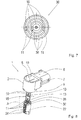
- Fig. 7 shows a sectional view taken along in FIG Fig. 5 shown section line VII-VII, wherein the first surface side 34 of the circuit board 30 is shown in a plan view.
- the second connection points 36 are arranged on the first surface side 34.
- the second connection points 36 are each in the form of an annular conductor track which, starting from a common center point, has a different radius relative to one another.
- the common center of the annular tracks corresponds to a center of the circular circuit board 30.
- the second connection points 36 are electrically isolated from each other by the respective different radius and the associated spaced-apart arrangement.
- the second connection points 36 form a sliding contact conductor track, on which the respective second contact side 11 of the contact elements 10 produces an electrical sliding contact.
- the contact elements 10 are rod-shaped with a rectangular cross-section, wherein the respective second contact side 11 having end portion L-shaped, wherein the second contact side 11 is formed by the short leg of the L-shape.
- the second contact side 11 forms a sliding contact surface on one of the second connection point 36 facing surface side of the short leg.
- the second connection points 36 may be formed as solder pads, to produce a material connection with the respectively associated second contact sides 11 after completion of a relative positioning of the sensor device 20 to the connector device 9, for example by means of a soldering process. As a result, the electrical contact between the second connection points 36 and the respective associated second contact sides 11 can be fixed or secured.
- the positioning element 13 can likewise form a contact element 10, the positioning element 13 then having a first contact side electrically connected to the plug connection 6 and a second contact side electrically connected to a second connection point 36.
- the electrical contact with the associated second connection point can take place within the central passage of the printed circuit board 30 or on the surface side 32 of the printed circuit board 30 facing the sensor carrier 22.
- the second connection point can protrude into the passage, be arranged on an inner edge of the passage as an annular sliding contact path or the passage on the sensor carrier 22 facing surface side 32 of the circuit board 30.
- Fig. 8 shows a perspective view of the in Fig. 3
- the sensor carrier 22 is formed of a cylindrical body, wherein the contacts 26 from the front end with the sensor element receptacle to the opposite end face on which the circuit board 30 is arranged , extend along a surface side connecting the front ends.
- the surface side of the sensor carrier 22 is flat or flat.
- the contacts 26 can be formed by punched parts which are arranged in parallel to each other, extend along the surface side rectilinearly and spaced apart, and are bent into the respective end side end portion for electrical contacting.
- the sensor carrier 22 and the contacts 26 can be produced inexpensively.
- the sensor carrier 22 is made of a plastic-containing Material molded with electrical insulation properties.
- the sensor carrier 22 may have in a front side end region facing the printed circuit board 30 a space for accommodating electronic components which can be arranged on the second surface side 32 of the conductor bar 30.
- the printed circuit board 30 has corresponding printed conductors for the electrical contacting of the electronic components for this case.
- the printed circuit board 30 is further arranged transversely with the first surface side 34 and the second surface side 32 transversely, in particular orthogonal to an axis extending from the sensor element receiving to the front end of the sensor carrier 22 extending axis.
- Fig. 9 shows an enlarged view of the in Fig. 8
- the second connection points 36 are arranged on the first surface side 34 of the printed circuit board 30 in such a way that the sliding contact surface of the second connection points 36 is raised or raised with respect to the first surface side 34. This can ensure that the second contact pages 11 only contact the second connection points 36. In this way, a frictional effect can be reduced if the orientation of the sensor device 20 to the plug-in connection device 9 is tailored to requirements.
- the holding member 15 is disposed near the second contact sides 11. As a result, increased stability is achieved in the area of the second contact sides 11, as a result of which a lever effect acting on the second contact sides 11 can be counteracted in the need-based positioning.
- Fig. 10 shows a flowchart of a method 1000 for producing a sensor device according to a preferred embodiment.
- This may be, for example, a sensor device 1 as described above.
- the sensor device 1 has a first housing part 2, which may be, for example, the plug connection housing 2, and a second housing part 3, which may be, for example, the sensor housing 3, the second housing part 3 being connected to the first housing part 2 via a bayonet-type connection, for example as described above 40, 42 is connectable, wherein the bayonet-type connection 40, 42 is designed such that the first and second housing part 2, 3 are connected to each other in a first aligned relative position and in the connected state are captively rotatable relative to each other in a further relative position different from the first relative position.
- the bayonet-type connection 40, 42 is designed such that the first and second housing part 2, 3 are connected to each other in a first aligned relative position and in the connected state are captively rotatable relative to each other in a further relative position different from the
- the method 1000 has a first step 1100 of the relative alignment of the first housing part 2 to the second housing part 3, wherein the first housing part 2 is brought into a first relative position to the second housing part 3. Furthermore, the method 1000 has a second step 1200 of connecting the first housing part 2 to the second housing part 3 in the first relative position and a third step 1300 of relatively rotating the first housing part 2 to the second housing part 3 from the first relative position to a different one Relative position on.
- the sensor device described with the preferred embodiments may preferably be adopted as a speed sensor in a motor vehicle for detecting a rotational speed and / or a rotational direction of a rotating element.
- the sensor device described can be used in other application areas in which at least one speed detection or rotation detection is required, wherein the sensor device for evaluating the signals and the power supply via the plug connection with an evaluation circuit or the like is to be connected.
Applications Claiming Priority (1)
| Application Number | Priority Date | Filing Date | Title |
|---|---|---|---|
| DE102013223912.2A DE102013223912A1 (de) | 2013-11-22 | 2013-11-22 | Sensorvorrichtung und Verfahren zum Herstellen einer Sensorvorrichtung |
Publications (1)
| Publication Number | Publication Date |
|---|---|
| EP2876416A1 true EP2876416A1 (fr) | 2015-05-27 |
Family
ID=51752029
Family Applications (1)
| Application Number | Title | Priority Date | Filing Date |
|---|---|---|---|
| EP14189820.5A Withdrawn EP2876416A1 (fr) | 2013-11-22 | 2014-10-22 | Dispositif de détection et procédé de fabrication d'un dispositif de détection |
Country Status (2)
| Country | Link |
|---|---|
| EP (1) | EP2876416A1 (fr) |
| DE (1) | DE102013223912A1 (fr) |
Families Citing this family (1)
| Publication number | Priority date | Publication date | Assignee | Title |
|---|---|---|---|---|
| DE102022208543A1 (de) | 2022-08-17 | 2024-02-22 | Zf Friedrichshafen Ag | Sensor und Montageverfahren eines Sensors |
Citations (7)
| Publication number | Priority date | Publication date | Assignee | Title |
|---|---|---|---|---|
| EP1167916A2 (fr) * | 2000-06-27 | 2002-01-02 | Dr. Johannes Heidenhain GmbH | Boitier pour appareil de mesure d'angle |
| DE10221303A1 (de) | 2002-05-14 | 2003-11-27 | Valeo Schalter & Sensoren Gmbh | Sensor, insbesondere Ultraschallsensor, und Verfahren zur Herstellung |
| DE202005006379U1 (de) * | 2005-04-21 | 2006-08-24 | Hengstler Gmbh | Hohlwellen-Drehgeber mit Motorwellen-Schutzkappe |
| DE102006061644B3 (de) * | 2006-12-27 | 2008-01-31 | Siemens Ag | Impulsgeber mit einer Plombiervorrichtung |
| DE202008008915U1 (de) * | 2008-07-01 | 2009-11-19 | Hypertac Gmbh | Mehrteilige Gehäuse für elektrische Steckverbindungen |
| DE102009015989A1 (de) * | 2009-04-02 | 2010-10-07 | Audi Ag | Steckverbindungsvorrichtung |
| DE102011004914A1 (de) * | 2011-03-01 | 2012-09-06 | Ifm Electronic Gmbh | Sensor |
Family Cites Families (18)
| Publication number | Priority date | Publication date | Assignee | Title |
|---|---|---|---|---|
| DE8909902U1 (fr) * | 1989-08-18 | 1989-10-05 | Conducta Gmbh & Co, 7016 Gerlingen, De | |
| DE4232909C2 (de) * | 1992-10-01 | 1997-05-07 | Conducta Endress & Hauser | Kopfteil eines elektrochemischen Sensors |
| DE29721694U1 (de) * | 1997-12-09 | 1998-02-05 | Mannesmann Vdo Ag | Plombiervorrichtung für einen Drehwertgeber |
| EP0952448B1 (fr) * | 1998-04-23 | 2004-03-24 | Endress + Hauser Conducta Gesellschaft für Mess- und Regeltechnik mbH + Co.KG. | Dispositif de retenue pour capteur de mesure des fluides de traitement |
| DE19948106C2 (de) * | 1999-09-27 | 2003-07-24 | Heidenhain Gmbh Dr Johannes | Positionsmeßsystem |
| DE10156753A1 (de) * | 2001-11-19 | 2003-06-05 | Epcos Ag | Meßfühler und Meßfühleranordnung |
| DE10352159A1 (de) * | 2003-05-19 | 2004-12-30 | Endress + Hauser Conducta Gesellschaft für Mess- und Regeltechnik mbH + Co. KG | Steckverbinderkupplung |
| EP1482298A1 (fr) * | 2003-05-26 | 2004-12-01 | Sensorix | Arrangement pour la détermination en continu d'une substance |
| DE102004044890A1 (de) * | 2004-09-14 | 2006-03-30 | Endress + Hauser Gmbh + Co. Kg | Vorrichtung zur Bestimmung und/oder Überwachung mindestens einer Prozessgröße eines Mediums |
| DE102004063499A1 (de) * | 2004-12-24 | 2006-07-06 | Huba Control Ag | Durchflussmessgerät mit einsteckbarer Sensorbaugruppe |
| DE202005013904U1 (de) * | 2005-09-02 | 2006-02-09 | Elb-Form Ges.m.b.H. | Rohr mit Sensoradapter |
| DE102006022981B4 (de) * | 2006-05-15 | 2017-10-26 | Knick Elektronische Messgeräte GmbH & Co. KG | Sondeneinrichtung zur Messung von Prozessgrößen |
| DE202006013147U1 (de) * | 2006-08-26 | 2006-10-26 | Sick Ag | Stecker |
| DE102006048084A1 (de) * | 2006-10-11 | 2008-04-17 | Gustav Wahler Gmbh U. Co. Kg | Linearsensor |
| DE102006053399A1 (de) * | 2006-11-10 | 2008-05-15 | Endress + Hauser Gmbh + Co. Kg | Messsonde für ein Messgerät |
| DE102007037759A1 (de) * | 2007-08-10 | 2009-02-12 | Schaeffler Kg | Vorrichtung zum Bestimmen einer Schaltstellung eines mechanischen Systems |
| DE202007018962U1 (de) * | 2007-11-05 | 2010-04-01 | Digmesa Ag | Oberteil für einen Durchflussmesser und Durchflussmesser |
| DE202009009647U1 (de) * | 2008-10-02 | 2009-10-22 | Apel, Helga | Befüllstutzen |
-
2013
- 2013-11-22 DE DE102013223912.2A patent/DE102013223912A1/de active Pending
-
2014
- 2014-10-22 EP EP14189820.5A patent/EP2876416A1/fr not_active Withdrawn
Patent Citations (7)
| Publication number | Priority date | Publication date | Assignee | Title |
|---|---|---|---|---|
| EP1167916A2 (fr) * | 2000-06-27 | 2002-01-02 | Dr. Johannes Heidenhain GmbH | Boitier pour appareil de mesure d'angle |
| DE10221303A1 (de) | 2002-05-14 | 2003-11-27 | Valeo Schalter & Sensoren Gmbh | Sensor, insbesondere Ultraschallsensor, und Verfahren zur Herstellung |
| DE202005006379U1 (de) * | 2005-04-21 | 2006-08-24 | Hengstler Gmbh | Hohlwellen-Drehgeber mit Motorwellen-Schutzkappe |
| DE102006061644B3 (de) * | 2006-12-27 | 2008-01-31 | Siemens Ag | Impulsgeber mit einer Plombiervorrichtung |
| DE202008008915U1 (de) * | 2008-07-01 | 2009-11-19 | Hypertac Gmbh | Mehrteilige Gehäuse für elektrische Steckverbindungen |
| DE102009015989A1 (de) * | 2009-04-02 | 2010-10-07 | Audi Ag | Steckverbindungsvorrichtung |
| DE102011004914A1 (de) * | 2011-03-01 | 2012-09-06 | Ifm Electronic Gmbh | Sensor |
Also Published As
| Publication number | Publication date |
|---|---|
| DE102013223912A1 (de) | 2015-05-28 |
Similar Documents
| Publication | Publication Date | Title |
|---|---|---|
| EP1173918B1 (fr) | Moteur electrique destine en particulier a monter et a descendre les vitres de vehicules a moteur | |
| DE4140403C2 (de) | Verfahren zur Montage eines Sensorkopfes für einen Magnetfeldgeber | |
| DE102008026470A1 (de) | Druckstück für eine Anschlussklemme | |
| DE102014215222A1 (de) | Getriebe-Antriebseinheit mit verrastbarer Elektronik-Schnittstelle | |
| DE19809492C2 (de) | Elektrischer Verbinder | |
| EP3000156B1 (fr) | Dispositif servant à établir un contact électrique entre un circuit imprimé et un moteur électrique | |
| EP2690412A9 (fr) | Capteur | |
| DE102007018762A1 (de) | Elektrische Kontaktstruktur in isolierenden Gehäusen | |
| DE102021103232B3 (de) | Anschlussvorrichtung für ein elektrisches und/oder elektronisches Gerät mit einem Gerätegehäuse, sowie Gerätegehäuseanordnung und Sensoranordnung | |
| DE102011119842B4 (de) | Elektrisches Verbindungselement und Leiterplattenanordnung | |
| DE102014215231B4 (de) | Getriebe-Antriebseinheit einschiebbaren Elektronikmodul | |
| EP2876415A1 (fr) | Dispositif de détection et procédé de fabrication d'un dispositif de détection | |
| EP2876416A1 (fr) | Dispositif de détection et procédé de fabrication d'un dispositif de détection | |
| EP2515388A1 (fr) | Dispositif de chauffage électrique | |
| DE102020202340A1 (de) | Antriebseinheit einer elektrischen Hilfskraftlenkung für ein Kraftfahrzeug | |
| DE102004001899A1 (de) | Sperrkreisanordnung | |
| EP1586491A1 (fr) | Connection electrique d'un groupe moto-pompe pour un ABS | |
| DE10017319C2 (de) | Anordnung zur elektrischen Kontaktierung | |
| DE102005005705A1 (de) | Kontaktierungsmittel für flexible elektrische Flachbandkabel | |
| DE102015225159A1 (de) | Magnetfeldsensor mit einem Steckersockel | |
| EP3175204B1 (fr) | Moyen de détection pour véhicule automobile | |
| EP3067670A1 (fr) | Composant de connecteur pour un capteur et procede de montage d'un composant de connecteur pour un capteur | |
| DE10161102A1 (de) | Leitungs-Steckverbindung für elektrisches Steuergerät sowie Herstellungsverfahren | |
| DE102013114024B4 (de) | Programmierbare Elektronikbaugruppe und bürstenloser Kleinstmotor | |
| DE102007047295A1 (de) | Wicklungsanschlussvorrichtung für einen elektrischen Motor oder Generator |
Legal Events
| Date | Code | Title | Description |
|---|---|---|---|
| PUAI | Public reference made under article 153(3) epc to a published international application that has entered the european phase |
Free format text: ORIGINAL CODE: 0009012 |
|
| 17P | Request for examination filed |
Effective date: 20141022 |
|
| AK | Designated contracting states |
Kind code of ref document: A1 Designated state(s): AL AT BE BG CH CY CZ DE DK EE ES FI FR GB GR HR HU IE IS IT LI LT LU LV MC MK MT NL NO PL PT RO RS SE SI SK SM TR |
|
| AX | Request for extension of the european patent |
Extension state: BA ME |
|
| STAA | Information on the status of an ep patent application or granted ep patent |
Free format text: STATUS: THE APPLICATION IS DEEMED TO BE WITHDRAWN |
|
| 18D | Application deemed to be withdrawn |
Effective date: 20151128 |
|
| RIN1 | Information on inventor provided before grant (corrected) |
Inventor name: DEICHLER, THOMAS |