EP2690412A9 - Capteur - Google Patents
Capteur Download PDFInfo
- Publication number
- EP2690412A9 EP2690412A9 EP12177898.9A EP12177898A EP2690412A9 EP 2690412 A9 EP2690412 A9 EP 2690412A9 EP 12177898 A EP12177898 A EP 12177898A EP 2690412 A9 EP2690412 A9 EP 2690412A9
- Authority
- EP
- European Patent Office
- Prior art keywords
- housing
- circuit board
- sensor
- printed circuit
- sensor element
- Prior art date
- Legal status (The legal status is an assumption and is not a legal conclusion. Google has not performed a legal analysis and makes no representation as to the accuracy of the status listed.)
- Granted
Links
- 238000004519 manufacturing process Methods 0.000 claims abstract description 10
- 150000001875 compounds Chemical class 0.000 claims description 42
- 238000004382 potting Methods 0.000 claims description 39
- 238000005266 casting Methods 0.000 claims description 28
- 229910052751 metal Inorganic materials 0.000 claims description 14
- 239000002184 metal Substances 0.000 claims description 14
- 238000000034 method Methods 0.000 claims description 6
- 229910000679 solder Inorganic materials 0.000 claims description 4
- 239000013307 optical fiber Substances 0.000 claims 1
- 239000004033 plastic Substances 0.000 description 12
- 238000003825 pressing Methods 0.000 description 9
- 230000001939 inductive effect Effects 0.000 description 6
- 239000000853 adhesive Substances 0.000 description 4
- 230000001070 adhesive effect Effects 0.000 description 4
- 230000003287 optical effect Effects 0.000 description 4
- HCHKCACWOHOZIP-UHFFFAOYSA-N Zinc Chemical compound [Zn] HCHKCACWOHOZIP-UHFFFAOYSA-N 0.000 description 3
- 238000004512 die casting Methods 0.000 description 3
- 230000007613 environmental effect Effects 0.000 description 3
- 238000005476 soldering Methods 0.000 description 3
- 229910052725 zinc Inorganic materials 0.000 description 3
- 239000011701 zinc Substances 0.000 description 3
- PXHVJJICTQNCMI-UHFFFAOYSA-N Nickel Chemical compound [Ni] PXHVJJICTQNCMI-UHFFFAOYSA-N 0.000 description 2
- 229910001297 Zn alloy Inorganic materials 0.000 description 2
- 239000004020 conductor Substances 0.000 description 2
- 238000001746 injection moulding Methods 0.000 description 2
- 239000007788 liquid Substances 0.000 description 2
- 238000003754 machining Methods 0.000 description 2
- 239000012778 molding material Substances 0.000 description 2
- 238000009757 thermoplastic moulding Methods 0.000 description 2
- 238000010136 thermoset moulding Methods 0.000 description 2
- 230000015572 biosynthetic process Effects 0.000 description 1
- 230000000295 complement effect Effects 0.000 description 1
- 238000001514 detection method Methods 0.000 description 1
- 238000009713 electroplating Methods 0.000 description 1
- 238000002347 injection Methods 0.000 description 1
- 239000007924 injection Substances 0.000 description 1
- 238000003780 insertion Methods 0.000 description 1
- 230000037431 insertion Effects 0.000 description 1
- 230000013011 mating Effects 0.000 description 1
- 238000000465 moulding Methods 0.000 description 1
- 229910052759 nickel Inorganic materials 0.000 description 1
- 239000011347 resin Substances 0.000 description 1
- 229920005989 resin Polymers 0.000 description 1
- 239000000126 substance Substances 0.000 description 1
- 229920001169 thermoplastic Polymers 0.000 description 1
- 239000012815 thermoplastic material Substances 0.000 description 1
- 239000004416 thermosoftening plastic Substances 0.000 description 1
Images

Classifications
-
- G—PHYSICS
- G01—MEASURING; TESTING
- G01D—MEASURING NOT SPECIALLY ADAPTED FOR A SPECIFIC VARIABLE; ARRANGEMENTS FOR MEASURING TWO OR MORE VARIABLES NOT COVERED IN A SINGLE OTHER SUBCLASS; TARIFF METERING APPARATUS; MEASURING OR TESTING NOT OTHERWISE PROVIDED FOR
- G01D11/00—Component parts of measuring arrangements not specially adapted for a specific variable
- G01D11/24—Housings ; Casings for instruments
- G01D11/245—Housings for sensors
-
- H—ELECTRICITY
- H03—ELECTRONIC CIRCUITRY
- H03K—PULSE TECHNIQUE
- H03K17/00—Electronic switching or gating, i.e. not by contact-making and –breaking
- H03K17/94—Electronic switching or gating, i.e. not by contact-making and –breaking characterised by the way in which the control signals are generated
- H03K17/945—Proximity switches
- H03K17/955—Proximity switches using a capacitive detector
-
- H—ELECTRICITY
- H03—ELECTRONIC CIRCUITRY
- H03K—PULSE TECHNIQUE
- H03K2217/00—Indexing scheme related to electronic switching or gating, i.e. not by contact-making or -breaking covered by H03K17/00
- H03K2217/94—Indexing scheme related to electronic switching or gating, i.e. not by contact-making or -breaking covered by H03K17/00 characterised by the way in which the control signal is generated
- H03K2217/96—Touch switches
- H03K2217/9607—Capacitive touch switches
- H03K2217/960755—Constructional details of capacitive touch and proximity switches
-
- Y—GENERAL TAGGING OF NEW TECHNOLOGICAL DEVELOPMENTS; GENERAL TAGGING OF CROSS-SECTIONAL TECHNOLOGIES SPANNING OVER SEVERAL SECTIONS OF THE IPC; TECHNICAL SUBJECTS COVERED BY FORMER USPC CROSS-REFERENCE ART COLLECTIONS [XRACs] AND DIGESTS
- Y10—TECHNICAL SUBJECTS COVERED BY FORMER USPC
- Y10T—TECHNICAL SUBJECTS COVERED BY FORMER US CLASSIFICATION
- Y10T29/00—Metal working
- Y10T29/49—Method of mechanical manufacture
- Y10T29/49002—Electrical device making
- Y10T29/49117—Conductor or circuit manufacturing
- Y10T29/49124—On flat or curved insulated base, e.g., printed circuit, etc.
- Y10T29/49128—Assembling formed circuit to base
Definitions
- the present invention relates to a sensor according to claim 1 and a method for producing a sensor according to the preamble of claim 14.
- Sensors for example optical, inductive or capacitive sensors, are used in various technical applications for the detection of physical or chemical parameters.
- the housing serves to protect electronic components on a printed circuit board and a sensor element from damaging environmental influences.
- the electronic components inside the housing are to be supplied with electric current. For this reason, it is necessary to guide electrical contacts through a housing wall of the housing in order to be able to supply the sensor from the outside with electrical current at an outer part of the contact parts.
- the circuit board with the electronic components and the sensor element are usually enveloped by a potting compound.
- the potting compound serves, on the one hand, to fix the printed circuit board and the sensor element in a positive and cohesive manner and, on the other hand, to keep out damaging environmental influences, for example liquids, from the printed circuit board and the sensor element.
- This is a fluid-tight sensor.
- the printed circuit board Before casting the sensor with the potting compound, it is necessary to connect the circuit board and the sensor element with the housing directly or indirectly for positioning the circuit board and / or the sensor element during the potting of the housing interior with potting compound.
- the printed circuit board Before casting with casting compound, the printed circuit board is generally connected to the electrical contacts of the sensor, generally by means of soldering. In an adhesive bond between the Printed circuit board and / or the sensor element and the housing before potting with potting compound, this adhesive connection is complicated and expensive to manufacture and has low flexibility for different types of sensors.
- the DE 195 44 815 C1 shows a sensor with a carrier disposed on an electrical circuit, which is connected to an electrical connection element and with a sensor element. Furthermore, a housing with an interior for receiving the carrier is shown, which in each case has an opening for the connection element and for the sensor element. In this case, the sensor element and a first part of the carrier are embedded in a thermoset molding compound. A second part of the carrier and the electrical connection element are enclosed by a thermoplastic molding compound. In a gap, adjacent to the opening for the sensor element, between the thermoset molding compound and the housing, a seal is arranged.
- the DE 100 13 218 C2 shows a method for producing a position sensor with a housing in the housing interior an electrical circuit arranged on a support sits, comprising the steps: the carrier is connected to a plug insert as an electrical connection element to a carrier-connection element combination, wherein the connection element rigidly with connected to the carrier, the carrier-connection element combination is introduced into the housing closed at a measuring end from a rear end opposite the measuring end, the space around the carrier-connection element combination in the housing interior is filled to a certain level with a molding compound, with the rear end of the housing, a cap is connected before curing of the molding material, through which the terminals of the connection element are guided, and with which the carrier-connection element combination is fixed in the housing.
- the object of the present invention is to provide a sensor and a method for producing a sensor, in which a printed circuit board and / or a sensor element with a low technical complexity can be reliably attached to the housing prior to casting with potting compound.
- a sensor comprising at least one housing, which encloses a housing interior, a printed circuit board with electronic components, which is arranged within the housing interior, a sensor element, which is electrically connected to the circuit board and is disposed within the housing interior, wherein the sensor element positively connected to the housing, so that the sensor element is held in the housing interior in position.
- the sensor element can thus first be fixed simply and inexpensively to the housing by means of a frictional connection, in particular a latching, click or press connection. Subsequently, a casting of the housing interior with a potting compound, for example, a thermoplastic molding material or a casting resin, take place.
- a frictional connection in particular a latching, click or press connection.
- the circuit board is non-positively connected to the housing.
- the printed circuit board and the sensor element can be exclusively positively connected to the housing, in particular apart from the cohesive connection due to the potting compound and / or apart from a mechanical connection to, in particular exclusive, electrical connection of the circuit board and / or the sensor element.
- the housing is preferably designed as a housing pot and substantially cuboid.
- the housing consists at least partially, in particular completely, of metal and / or plastic.
- the housing can be made in several parts.
- the housing may be in the area of Sensor element may be formed as a translucent or opaque cap.
- the cap made of plastic and the rest of the housing are made of metal.
- the sensor may be an optical, inductive or capacitive sensor.
- the housing also has a housing cover.
- the printed circuit board comprises printed conductors and the electronic components are electrically and mechanically connected to the printed circuit board.
- the circuit board is disposed entirely within the housing interior enclosed by the housing.
- the circuit board and / or the sensor element can be completely enclosed by the potting compound. As a result, no damaging environmental influences, for example a liquid, can reach the printed circuit board and / or the sensor element. It is in this case a liquid- or fluid-tight sensor, which is particularly splash-proof.
- At least one positive locking geometry is formed on the housing and at least one counter-form-locking geometry is formed on the printed circuit board, with the at least one form-fitting and counter-form-fitting geometry frictionally engaging with one another for connecting the printed circuit board to the housing.
- the positive locking geometry is preferably designed as a connecting cam and / or a locking shoulder.
- As Gegenform gleichgeometrie an opening and / or a latch can be formed.
- a frictional connection is preferably carried out due to a press connection of form-locking geometry and counter-form-fitting geometry.
- the present inventive sensor is at the at least one GegenformQuerygeometrie ever an electrical circuit board contact element for electrically conductive connection of the circuit board to the housing on the formed at least one form fit geometry. This can additionally be made available between the circuit board and the housing an electrically conductive connection.
- the ever an electrical circuit board contact element can be designed here as a metal ring. If the housing consists at least partially, in particular completely, of metal, cable-bound radio-frequency interference can be conducted from the printed circuit board to the housing in an advantageous manner.
- this electrical connection between the circuit board and the housing is particularly reliable, because due to the non-positive connection, for example a press connection, constantly a mechanical and thus an electrical contact between the Printed circuit board contact element on the Gegenform gleichgeometrie and the positive locking geometry, for example, the connecting cam exists.
- the sensor element is a coil and the sensor is an inductive proximity sensor or the sensor element is an LED and / or a phototransistor and the sensor is an optical sensor.
- the housing is transparent to the LED and / or phototransistor.
- the senor element is held elastically biased by means of an elastic element between the housing and the elastic element.
- the elastic element may in this case be designed as a spring.
- the sensor element is located on a first end directly or indirectly on the housing, in particular the cap, and due to the geometry of the housing, for example as a recess, the sensor element is positively held on the housing.
- the elastic element can also rest on a second end directly or indirectly on the sensor element.
- the first and second ends may be opposite to one another Be formed sensor element.
- the sensor element may comprise two sensor element contact elements for electrical connection of the sensor element.
- the sensor element contact elements can also be materially connected, for example with a solder connection, to the printed circuit board, in particular printed circuit board contact elements, electrically connected.
- the sensor element for example, indirectly connected to a plug-in part frictionally under elastic bias to the elastic element.
- a resilient bias of the elastic member is for example possible because due to a non-positive connection, in particular a press connection between the form and Gegenform gleichgeometrie forces from the elastic element on the circuit board and from the circuit board to the housing can be transferred.
- the housing has a plug opening, with which a plug sleeve is in particular non-positively connected.
- the frictional connection can be effected by means of a press connection.
- a plug part for example made of plastic, arranged with electrical contact elements as electrical contacts.
- the plug sleeve can be made of metal.
- a cable seal made of plastic can be provided at the plug opening, are guided by the electric power cable as electrical contacts.
- the sensor expediently comprises a light guide and a light transmitter, for example an LED, so that the light generated by the light transmitter outside the sensor can be conducted from the light transmitter through the light guide.
- the light guide is arranged on the outside on two or three sides of the sensor, so that the light emitted by the light emitter light is visible on two or three sides of the sensor.
- a frictional connection which serves to electrically connect the circuit board and / or the sensor element, for example with the contacts for the electrical supply of the sensor, is not taken into consideration.
- mechanical connection to the electrical connection also constitute mechanical connections, they can provide no or substantially no contribution to a sufficient mechanical attachment or positioning of the printed circuit board and / or the sensor element before casting with the potting compound due to their mechanical properties.
- the housing can be injection molded, for.
- As plastic in particular thermoplastic, or metal, eg. As zinc or a zinc alloy, provided and preferably the housing is coated after injection molding, in particular by means of electroplating, z. As with metal, especially nickel.
- the housing is expediently made available as a housing pot and / or the housing is provided with a cap opening and / or the housing is provided with a plug opening; in particular, at least one pressing shoulder, preferably two pressing shoulders, is formed on the plug opening.
- the cap opening can be closed with a cap, in particular the cap positively and / or non-positively, for example with a latching connection, is connected to the housing, in particular before casting with potting compound.
- a plug sleeve can further be inserted, wherein the plug sleeve is connected to the housing at the plug opening with a positive and / or non-positive connection, in particular a press connection, so that in particular at least one counterpressive shoulder, preferably at least two counterpressive heels on the Plug sleeve on the at least one pressing paragraph, preferably two pressing paragraphs, rest on the plug opening of the housing, in particular before casting with potting compound.
- a cable seal can be inserted and positively and / or positively and / or materially connected to the housing at the plug opening, in particular before casting with potting compound. Due to the Pressabsatzes on the housing and the Gegenpressabsatzes on the plug sleeve, preferably made of metal, thereby a sufficient press connection can be made available and produced at a small housing wall thickness at the plug opening.
- the press sales and the counter press sales thus an additional pressing surface in addition to the normal press opening at the plug opening of the corresponding housing wall, for example, rear wall of the housing available.
- a plug part, z. B. plastic introduced with the electrical contact elements as contacts and positively and / or positively and / or materially connected to the plug sleeve, in particular after connecting the plug sleeve to the housing at the plug opening, in particular before casting with potting compound.
- power cables can be routed through a cable opening, in particular after connecting the cable seal to the housing at the plug opening, in particular before casting with potting compound.
- the sensor element is connected to the housing by the sensor element between the housing, in particular the cap, and an elastic member, in particular a spring, is elastically biased, in particular before casting with potting compound, and / or the circuit board on at least one housing paragraph, in particular at least two housing heels, placed, in particular before casting with potting compound, and / or the circuit board is positively connected to at least one form fit geometry of at least one GegenformQuerygeometrie on the housing, in particular at least one connecting cam, preferably two connecting cams on the Housing in at least one opening, in particular two openings are introduced on the circuit board, in particular before casting with potting compound.
- the at least one interlocking geometry on the printed circuit board is additionally frictionally connected to the at least one counterframe geometry on the printed circuit board, in particular by at least one connecting cam being pressed against the housing with the printed circuit board at the opening, in particular before casting with potting compound, and / or the elastic element is cohesively, for example by means of soldering, connected to the circuit board and / or sensor element contact elements on the sensor element are electrically connected to the printed circuit board, in particular by soldering the sensor element contact elements with printed circuit board contact elements, in particular before casting with potting compound, and / or the electrical contacts are electrically connected to the circuit board, in particular soldered by the contacts with PCB contact elements be, especially before casting with potting compound.
- a light guide in particular before casting with potting compound, non-positively connected to the housing, for example with a latching connection, in particular before casting with potting compound.
- the housing pot comprises only one opening for insertion of the printed circuit board.
- the senor is fluid-tight, in particular the printed circuit board with electronic components and / or the sensor element are enveloped or embedded in a fluid-tight manner by the potting compound.
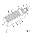
- An in Fig. 7 and 8th illustrated sensor 1 is designed as an inductive sensor 2 and thus represents a proximity sensor. With the inductive sensor 2 objects can be detected in the area or in the vicinity thereof.
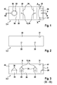
- the sensor 1,2 comprises a housing 3, which is designed as a housing pot 4 (shown in FIG Figure 3 ).
- the housing 3 is made of metal, namely a zinc alloy, and is manufactured by means of a zinc die casting process.
- the housing pot 4 ( Fig. 1 to 4 ) includes a housing interior 6.
- the housing interior 6 is bounded by a bottom wall 38, two side walls 39, a front wall 40 and a rear wall 41 of the housing pot 4.
- On the bottom wall 38 two housing heels 34 are formed in the transverse direction.
- a connecting cam 16 is designed as a positive locking geometry 15 for supporting a printed circuit board 8 in each case.
- a mounting hole 30 is provided in each case in the transverse direction.
- the mounting holes 30 preferably have a thread.
- the bottom wall 38 further includes a cap opening 35.
- the housing 3 has a cap ring 36.
- a plug opening 5 on the rear wall 41 serves to introduce a plug sleeve 26.
- a pressing shoulder 29 is formed on the housing 3 in the region of the plug opening 5 at the bottom. The press shoulder 29 serves to produce an additional pressing surface between the housing 3 and the plug sleeve 26 in a production and connection of the plug sleeve 26 with the housing 3 at the plug opening 5.
- the two side walls 39 have at the top two housing recesses 31 for a light guide 28.
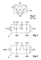
- the printed circuit board 8 On the printed circuit board 8 ( FIGS. 5 and 6 ), four electronic components 9, for example a controller and an electrical resistor, are mechanically and electrically connected to the printed circuit board 8 on the upper side.
- the printed circuit board 8 has printed conductors, not shown for this purpose.
- At the bottom of the printed circuit board 8 ( Fig. 6 ) are two electronic components 9 to the circuit board 8 mechanically and electrically connected.
- the printed circuit board 8 made of plastic has two openings 18 which form a Gegenform gleichgeometrie 17.
- additional metal rings 20 are arranged as printed circuit board contact elements 19 at these openings 18 of the printed circuit board 8.
- the metal rings 20 are electrically conductively connected to the respective connection cam 16. This can be derived via the housing 3 in an advantageous manner interference voltages.
- a spring 22 is attached as an elastic element 21 on the underside of the printed circuit board 8.
- the attachment is realized in this embodiment by means of a solder joint.
- the circuit board 8 also has at the top, as shown in FIG. 5 right, three PCB contact elements 19 on.
- the three printed circuit board contact elements 19 are U-shaped in cross-section ( Fig. 7 ) and thus also on the underside and thus also in Fig. 6 visible, noticeable.
- the geometry of the housing pot 4 described above for example with the housing heels 34 and the cap opening 35 with the cap ring 36, can already be easily produced in the die-casting process, without subsequent machining, for example by machining , is required.
- a cap 14 made of plastic is inserted and pressed into the cap opening 35 on the bottom wall 38 of the housing 3, so that a positive and / or non-positive connection between the cap 14 and the cap ring 36 is made on the housing 3.
- the cap ring 36 provides a relatively large connection area between the cap 14 and the housing 3, that is, the cap ring 36 available.
- the plug sleeve 26 is inserted from metal into the plug opening 5 on the rear wall 41 and pressed, so that a press connection between the plug sleeve 26 and the housing 3 is made. Due to the pressing paragraph 29 on the housing 3 and a counter-pressing shoulder on the plug sleeve 26 is a large press-bonding surface between the plug sleeve 26 and the housing 3 is available. As a result, the thickness of the rear wall 41 has the same thickness as the other walls of the housing 3.
- a plug part 27 made of plastic is inserted into the plug sleeve 26.
- the plug part 27 is made of thermoplastic material by means of injection molding. In this case, three electrical contact elements 13 are encapsulated as electrical contacts 12 of the plastic of the connector part 27.
- the electrical contact elements 13 serve to electrically connect the sensor 1 to the environment.
- three electrical contact elements 13 are integrated into the plug part 27, of which, however, due to the sectional formation in Fig. 7 only an electrical contact element 13 is shown.
- the electrical contact elements 13 are on the in Fig. 7 arranged right end outside of the sensor 1 and can thereby be mechanically and electrically connected to corresponding electrical contact counter-elements (not shown).
- a corresponding electrical mating connector (not shown) on an external thread 37 of the connector sleeve 26 screwed.
- the electrical contact counter-elements can be connected to the electrical contact elements 13.
- the plug part 27 is positively and / or non-positively connected, for example by means of a latching connection, with the plug sleeve 26.
- a coil 11 is placed as a sensor element 10 for the inductive sensor 2 on the cap 14.
- the sensor element 10 can be designed as an LED and / or a phototransistor.
- the cap 14 in this case has a corresponding geometry, so that on the cap 14 on the inside a recess 23 is formed which is complementary to the geometry of the coil 11 is formed. Thus, the coil 11 is held positively in the recess 23 of the cap 14.
- the circuit board 8 is placed on the housing 3 by first the two connecting cam 16 is inserted into the two openings 18 of the circuit board 8 and then the circuit board 8 is placed on the two housing sections 34. This results in a positive connection between the circuit board 8 and the housing 3 to the connection cam 16 and the housing paragraphs 34. In addition, a press connection between the connection cam 16 and the opening 18 on the circuit board 8 is still made by means of a corresponding tool.
- the openings 18 each have metal rings 20 on the printed circuit board 8. This results in a frictional connection between the housing 3 and the circuit board. 8
- the coil 11 is placed on the cap 14.
- An intermediate part 24 in turn is for fitting to a second end 33, the upper end of the coil 11, as shown in FIG Fig. 7 , intended.
- the intermediate part 24 is made of plastic.
- the coil 11 For electrically connecting the coil 11 to the printed circuit board 8, the coil 11 has two contact elements 25 for connecting the coil 11, which in Fig. 7 are shown in dashed lines. These two contact elements 25 for connecting the coil 11 are then connected to the two in Fig. 5 soldered on the left shown PCB contact elements 19, so that thereby the coil 11 is electrically and slightly mechanically connected to the circuit board 8 and the printed circuit board contact elements 19.
- a light guide 28 made of a light-conducting plastic with the two housing recesses 31 on the two side walls 39 is further connected on the upper side, for example by means of a clip or locking connection.
- the housing interior 6 is poured with the potting compound 7, so that thereby the circuit board 8 and the coil 11 are completely enclosed by the potting compound 7.
- the sensor 1 constitutes a fluid-tight sensor 1.
- a cable seal is arranged in the plug opening 5 instead of the plug sleeve 26 and the plug part 27.
- the cable seal is designed as a socket with a cable opening and through this cable opening three power cables can be performed as electrical contacts 12. These power cables are at one end with the three in FIGS. 5 and 6 soldered on the right printed circuit board contact elements 19. At the right ends of the power cables they can be connected for example by means of an electrical screw with a corresponding unit outside the sensor 1.
- the gap or space between the cable opening and the power cables is sealed during pouring with the potting compound 7 and closed.
- the flowability or toughness of the potting compound 7 before hardening is designed so that no or substantially no potting compound 7 passes from these residual openings through the cable opening.
- the circuit board 8 and the coil 11 are positively or non-positively connected directly or indirectly with the housing 3 before casting with the potting compound 7. Thereby, the circuit board 8 and the coil 11 can be easily and inexpensively held before casting with the potting compound 7 on the housing 3 and thus positioned in the housing interior 6. Elaborate adhesive bonds before casting with the potting compound 7 between the circuit board 8 and / or the coil 11 are not required. In addition, advantageously different sensors 1 can be produced in a flexible manner with the same production method.
Landscapes
- Physics & Mathematics (AREA)
- General Physics & Mathematics (AREA)
- Casings For Electric Apparatus (AREA)
- Switches That Are Operated By Magnetic Or Electric Fields (AREA)
- Optical Transform (AREA)
Priority Applications (2)
| Application Number | Priority Date | Filing Date | Title |
|---|---|---|---|
| EP12177898.9A EP2690412B1 (fr) | 2012-07-25 | 2012-07-25 | Capteur |
| US13/949,688 US9423280B2 (en) | 2012-07-25 | 2013-07-24 | Sensor |
Applications Claiming Priority (1)
| Application Number | Priority Date | Filing Date | Title |
|---|---|---|---|
| EP12177898.9A EP2690412B1 (fr) | 2012-07-25 | 2012-07-25 | Capteur |
Publications (3)
| Publication Number | Publication Date |
|---|---|
| EP2690412A1 EP2690412A1 (fr) | 2014-01-29 |
| EP2690412A9 true EP2690412A9 (fr) | 2014-10-01 |
| EP2690412B1 EP2690412B1 (fr) | 2018-04-18 |
Family
ID=46845587
Family Applications (1)
| Application Number | Title | Priority Date | Filing Date |
|---|---|---|---|
| EP12177898.9A Active EP2690412B1 (fr) | 2012-07-25 | 2012-07-25 | Capteur |
Country Status (2)
| Country | Link |
|---|---|
| US (1) | US9423280B2 (fr) |
| EP (1) | EP2690412B1 (fr) |
Families Citing this family (7)
| Publication number | Priority date | Publication date | Assignee | Title |
|---|---|---|---|---|
| DE102016210532B4 (de) * | 2016-06-14 | 2020-11-26 | Robert Bosch Gmbh | Sensoranordnung |
| DE102016218179A1 (de) * | 2016-09-21 | 2018-03-22 | Brose Fahrzeugteile Gmbh & Co. Kommanditgesellschaft, Bamberg | Kapazitiver Näherungssensor |
| DE102016220773A1 (de) * | 2016-10-21 | 2018-04-26 | Ifm Electronic Gmbh | Verfahren zur Endfertigung eines Näherungsschalters zur berührungslosen Erfassung eines Targets in einem Überwachungsbereich und Näherungsschalter zur berührungslosen Erfassung eines Targets in einem Überwachungsbereich |
| DE102018101690B3 (de) * | 2018-01-25 | 2019-06-06 | Logicdata Electronic & Software Entwicklungs Gmbh | Elektronische Komponente eines verstellbaren Möbelsystems, Möbelsystem, Anordnung und Verfahren zur Konfiguration einer elektronischen Komponente |
| FR3083616A1 (fr) * | 2018-07-06 | 2020-01-10 | Airbus Operations | Structure d’aeronef comprenant un capteur avec un systeme de jonction ameliore et aeronef comprenant ladite structure |
| DE102018124845A1 (de) * | 2018-10-09 | 2020-04-09 | Sick Ag | Sensoreinheit |
| DE102021101181B4 (de) * | 2021-01-21 | 2022-09-08 | Sick Ag | Gehäuse für einen induktiven Sensor und ein Verfahren zur Herstellung eines Gehäuses füreinen induktiven Sensor |
Family Cites Families (6)
| Publication number | Priority date | Publication date | Assignee | Title |
|---|---|---|---|---|
| DE19544815C1 (de) * | 1995-12-01 | 1997-04-10 | Balluff Gebhard Gmbh & Co | Sensor und Verfahren zu seiner Herstellung |
| WO1999040285A1 (fr) * | 1998-02-05 | 1999-08-12 | Robert Bosch Gmbh | Module electronique pour unite d'entrainement commandee par un moteur electrique |
| DE10013218C2 (de) | 2000-03-17 | 2003-06-05 | Balluff Gmbh | Verfahren zur Herstellung eines Positionssensors und Positionssensor |
| DE102005053792B4 (de) * | 2005-11-09 | 2009-02-19 | Diehl Ako Stiftung & Co. Kg | Kapazitiver Berührungsschalter |
| DE102008040156A1 (de) * | 2008-07-03 | 2010-01-07 | Robert Bosch Gmbh | Steuergerät für Personenschutzmittel für ein Fahrzeug und ein Verfahren zum Zusammenbau eines solchen Steuergeräts |
| US9194726B2 (en) * | 2010-12-17 | 2015-11-24 | Aktiebolaget Skf | Support member, detection set comprising such a support member, manufacturing method of such a detection set and bearing assembly including such a detection set |
-
2012
- 2012-07-25 EP EP12177898.9A patent/EP2690412B1/fr active Active
-
2013
- 2013-07-24 US US13/949,688 patent/US9423280B2/en not_active Expired - Fee Related
Also Published As
| Publication number | Publication date |
|---|---|
| US9423280B2 (en) | 2016-08-23 |
| EP2690412B1 (fr) | 2018-04-18 |
| EP2690412A1 (fr) | 2014-01-29 |
| US20140026656A1 (en) | 2014-01-30 |
Similar Documents
| Publication | Publication Date | Title |
|---|---|---|
| EP2690412B1 (fr) | Capteur | |
| EP1718937B1 (fr) | Support de capteur et procede de realisation associe | |
| DE202015007010U1 (de) | Verbinder | |
| EP1695037B1 (fr) | Procede pour produire un appareil de commutation, et composant pour cet appareil de commutation | |
| WO2007131374A1 (fr) | Interrupteur de proximité et procédé de mise en contact d'une carte à circuit imprimé de capteur | |
| EP3613110B1 (fr) | Assemblage d'une pièce de connecteur à fiches avec insert de contact et élément de mise à la terre | |
| DE102013101823B4 (de) | Kontaktträger mit einem Unterteil | |
| EP1728414B1 (fr) | Dispositif comprenant un moteur electrique et une carte de circuits imprimes principale et procede de montage | |
| EP2520142B2 (fr) | Capteur doté d'un boîtier et procédé de fabrication correspondant | |
| WO2007113030A1 (fr) | Module de raccordement pour raccorder une unité de commande ou équivalent à une unité d'entraînement | |
| DE10039588B4 (de) | Gebereinrichtung | |
| DE102008059661B4 (de) | Optischer Sensor | |
| DE202004002348U1 (de) | Kurbelwellengeber | |
| DE19544660A1 (de) | Steckeranordnung für ein elektrisches Gerät | |
| DE102011110637B4 (de) | Steckverbinder | |
| EP1139493A2 (fr) | Connecteur électrique pour le raccordement de câbles à un appareil | |
| EP3067670B1 (fr) | Composant de connecteur pour un capteur et procede de montage d'un composant de connecteur pour un capteur | |
| EP2690413B1 (fr) | Capteur | |
| EP2615426A1 (fr) | Capteur | |
| DE102008058926B4 (de) | Elektromotorische Antriebseinheit für Stellantriebe in Kraftfahrzeug | |
| DE102019102713A1 (de) | Antriebseinheit | |
| DE102012105352A1 (de) | Positionierelement | |
| WO2018046176A1 (fr) | Poignée de porte de véhicule | |
| DE102013101832B4 (de) | Kontaktträger mit einem Toleranzausgleichsabschnitt | |
| DE102011079377A1 (de) | Steckermodul, insbesondere für Fensterheberantriebe, sowie Verfahren zu dessen Herstellung |
Legal Events
| Date | Code | Title | Description |
|---|---|---|---|
| PUAI | Public reference made under article 153(3) epc to a published international application that has entered the european phase |
Free format text: ORIGINAL CODE: 0009012 |
|
| AK | Designated contracting states |
Kind code of ref document: A1 Designated state(s): AL AT BE BG CH CY CZ DE DK EE ES FI FR GB GR HR HU IE IS IT LI LT LU LV MC MK MT NL NO PL PT RO RS SE SI SK SM TR |
|
| AX | Request for extension of the european patent |
Extension state: BA ME |
|
| 17P | Request for examination filed |
Effective date: 20140728 |
|
| RBV | Designated contracting states (corrected) |
Designated state(s): AL AT BE BG CH CY CZ DE DK EE ES FI FR GB GR HR HU IE IS IT LI LT LU LV MC MK MT NL NO PL PT RO RS SE SI SK SM TR |
|
| 17Q | First examination report despatched |
Effective date: 20151001 |
|
| GRAP | Despatch of communication of intention to grant a patent |
Free format text: ORIGINAL CODE: EPIDOSNIGR1 |
|
| INTG | Intention to grant announced |
Effective date: 20180105 |
|
| GRAS | Grant fee paid |
Free format text: ORIGINAL CODE: EPIDOSNIGR3 |
|
| GRAA | (expected) grant |
Free format text: ORIGINAL CODE: 0009210 |
|
| AK | Designated contracting states |
Kind code of ref document: B1 Designated state(s): AL AT BE BG CH CY CZ DE DK EE ES FI FR GB GR HR HU IE IS IT LI LT LU LV MC MK MT NL NO PL PT RO RS SE SI SK SM TR |
|
| REG | Reference to a national code |
Ref country code: GB Ref legal event code: FG4D Free format text: NOT ENGLISH |
|
| REG | Reference to a national code |
Ref country code: CH Ref legal event code: EP |
|
| REG | Reference to a national code |
Ref country code: AT Ref legal event code: REF Ref document number: 990983 Country of ref document: AT Kind code of ref document: T Effective date: 20180515 |
|
| REG | Reference to a national code |
Ref country code: IE Ref legal event code: FG4D Free format text: LANGUAGE OF EP DOCUMENT: GERMAN |
|
| REG | Reference to a national code |
Ref country code: DE Ref legal event code: R096 Ref document number: 502012012544 Country of ref document: DE |
|
| REG | Reference to a national code |
Ref country code: FR Ref legal event code: PLFP Year of fee payment: 7 |
|
| REG | Reference to a national code |
Ref country code: NL Ref legal event code: MP Effective date: 20180418 |
|
| REG | Reference to a national code |
Ref country code: LT Ref legal event code: MG4D |
|
| PG25 | Lapsed in a contracting state [announced via postgrant information from national office to epo] |
Ref country code: NL Free format text: LAPSE BECAUSE OF FAILURE TO SUBMIT A TRANSLATION OF THE DESCRIPTION OR TO PAY THE FEE WITHIN THE PRESCRIBED TIME-LIMIT Effective date: 20180418 |
|
| PG25 | Lapsed in a contracting state [announced via postgrant information from national office to epo] |
Ref country code: NO Free format text: LAPSE BECAUSE OF FAILURE TO SUBMIT A TRANSLATION OF THE DESCRIPTION OR TO PAY THE FEE WITHIN THE PRESCRIBED TIME-LIMIT Effective date: 20180718 Ref country code: AL Free format text: LAPSE BECAUSE OF FAILURE TO SUBMIT A TRANSLATION OF THE DESCRIPTION OR TO PAY THE FEE WITHIN THE PRESCRIBED TIME-LIMIT Effective date: 20180418 Ref country code: FI Free format text: LAPSE BECAUSE OF FAILURE TO SUBMIT A TRANSLATION OF THE DESCRIPTION OR TO PAY THE FEE WITHIN THE PRESCRIBED TIME-LIMIT Effective date: 20180418 Ref country code: BG Free format text: LAPSE BECAUSE OF FAILURE TO SUBMIT A TRANSLATION OF THE DESCRIPTION OR TO PAY THE FEE WITHIN THE PRESCRIBED TIME-LIMIT Effective date: 20180718 Ref country code: SE Free format text: LAPSE BECAUSE OF FAILURE TO SUBMIT A TRANSLATION OF THE DESCRIPTION OR TO PAY THE FEE WITHIN THE PRESCRIBED TIME-LIMIT Effective date: 20180418 Ref country code: PL Free format text: LAPSE BECAUSE OF FAILURE TO SUBMIT A TRANSLATION OF THE DESCRIPTION OR TO PAY THE FEE WITHIN THE PRESCRIBED TIME-LIMIT Effective date: 20180418 Ref country code: ES Free format text: LAPSE BECAUSE OF FAILURE TO SUBMIT A TRANSLATION OF THE DESCRIPTION OR TO PAY THE FEE WITHIN THE PRESCRIBED TIME-LIMIT Effective date: 20180418 Ref country code: LT Free format text: LAPSE BECAUSE OF FAILURE TO SUBMIT A TRANSLATION OF THE DESCRIPTION OR TO PAY THE FEE WITHIN THE PRESCRIBED TIME-LIMIT Effective date: 20180418 |
|
| PG25 | Lapsed in a contracting state [announced via postgrant information from national office to epo] |
Ref country code: HR Free format text: LAPSE BECAUSE OF FAILURE TO SUBMIT A TRANSLATION OF THE DESCRIPTION OR TO PAY THE FEE WITHIN THE PRESCRIBED TIME-LIMIT Effective date: 20180418 Ref country code: LV Free format text: LAPSE BECAUSE OF FAILURE TO SUBMIT A TRANSLATION OF THE DESCRIPTION OR TO PAY THE FEE WITHIN THE PRESCRIBED TIME-LIMIT Effective date: 20180418 Ref country code: GR Free format text: LAPSE BECAUSE OF FAILURE TO SUBMIT A TRANSLATION OF THE DESCRIPTION OR TO PAY THE FEE WITHIN THE PRESCRIBED TIME-LIMIT Effective date: 20180719 Ref country code: RS Free format text: LAPSE BECAUSE OF FAILURE TO SUBMIT A TRANSLATION OF THE DESCRIPTION OR TO PAY THE FEE WITHIN THE PRESCRIBED TIME-LIMIT Effective date: 20180418 |
|
| PGFP | Annual fee paid to national office [announced via postgrant information from national office to epo] |
Ref country code: GB Payment date: 20180725 Year of fee payment: 7 |
|
| PG25 | Lapsed in a contracting state [announced via postgrant information from national office to epo] |
Ref country code: PT Free format text: LAPSE BECAUSE OF FAILURE TO SUBMIT A TRANSLATION OF THE DESCRIPTION OR TO PAY THE FEE WITHIN THE PRESCRIBED TIME-LIMIT Effective date: 20180820 |
|
| REG | Reference to a national code |
Ref country code: DE Ref legal event code: R097 Ref document number: 502012012544 Country of ref document: DE |
|
| PG25 | Lapsed in a contracting state [announced via postgrant information from national office to epo] |
Ref country code: EE Free format text: LAPSE BECAUSE OF FAILURE TO SUBMIT A TRANSLATION OF THE DESCRIPTION OR TO PAY THE FEE WITHIN THE PRESCRIBED TIME-LIMIT Effective date: 20180418 Ref country code: DK Free format text: LAPSE BECAUSE OF FAILURE TO SUBMIT A TRANSLATION OF THE DESCRIPTION OR TO PAY THE FEE WITHIN THE PRESCRIBED TIME-LIMIT Effective date: 20180418 Ref country code: RO Free format text: LAPSE BECAUSE OF FAILURE TO SUBMIT A TRANSLATION OF THE DESCRIPTION OR TO PAY THE FEE WITHIN THE PRESCRIBED TIME-LIMIT Effective date: 20180418 Ref country code: CZ Free format text: LAPSE BECAUSE OF FAILURE TO SUBMIT A TRANSLATION OF THE DESCRIPTION OR TO PAY THE FEE WITHIN THE PRESCRIBED TIME-LIMIT Effective date: 20180418 Ref country code: SK Free format text: LAPSE BECAUSE OF FAILURE TO SUBMIT A TRANSLATION OF THE DESCRIPTION OR TO PAY THE FEE WITHIN THE PRESCRIBED TIME-LIMIT Effective date: 20180418 |
|
| PLBE | No opposition filed within time limit |
Free format text: ORIGINAL CODE: 0009261 |
|
| STAA | Information on the status of an ep patent application or granted ep patent |
Free format text: STATUS: NO OPPOSITION FILED WITHIN TIME LIMIT |
|
| PG25 | Lapsed in a contracting state [announced via postgrant information from national office to epo] |
Ref country code: SM Free format text: LAPSE BECAUSE OF FAILURE TO SUBMIT A TRANSLATION OF THE DESCRIPTION OR TO PAY THE FEE WITHIN THE PRESCRIBED TIME-LIMIT Effective date: 20180418 Ref country code: IT Free format text: LAPSE BECAUSE OF FAILURE TO SUBMIT A TRANSLATION OF THE DESCRIPTION OR TO PAY THE FEE WITHIN THE PRESCRIBED TIME-LIMIT Effective date: 20180418 |
|
| 26N | No opposition filed |
Effective date: 20190121 |
|
| PG25 | Lapsed in a contracting state [announced via postgrant information from national office to epo] |
Ref country code: LU Free format text: LAPSE BECAUSE OF NON-PAYMENT OF DUE FEES Effective date: 20180725 Ref country code: MC Free format text: LAPSE BECAUSE OF FAILURE TO SUBMIT A TRANSLATION OF THE DESCRIPTION OR TO PAY THE FEE WITHIN THE PRESCRIBED TIME-LIMIT Effective date: 20180418 |
|
| REG | Reference to a national code |
Ref country code: BE Ref legal event code: MM Effective date: 20180731 |
|
| REG | Reference to a national code |
Ref country code: IE Ref legal event code: MM4A |
|
| PG25 | Lapsed in a contracting state [announced via postgrant information from national office to epo] |
Ref country code: IE Free format text: LAPSE BECAUSE OF NON-PAYMENT OF DUE FEES Effective date: 20180725 |
|
| PG25 | Lapsed in a contracting state [announced via postgrant information from national office to epo] |
Ref country code: SI Free format text: LAPSE BECAUSE OF FAILURE TO SUBMIT A TRANSLATION OF THE DESCRIPTION OR TO PAY THE FEE WITHIN THE PRESCRIBED TIME-LIMIT Effective date: 20180418 Ref country code: BE Free format text: LAPSE BECAUSE OF NON-PAYMENT OF DUE FEES Effective date: 20180731 |
|
| REG | Reference to a national code |
Ref country code: AT Ref legal event code: MM01 Ref document number: 990983 Country of ref document: AT Kind code of ref document: T Effective date: 20180725 |
|
| PG25 | Lapsed in a contracting state [announced via postgrant information from national office to epo] |
Ref country code: AT Free format text: LAPSE BECAUSE OF NON-PAYMENT OF DUE FEES Effective date: 20180725 |
|
| PG25 | Lapsed in a contracting state [announced via postgrant information from national office to epo] |
Ref country code: MT Free format text: LAPSE BECAUSE OF FAILURE TO SUBMIT A TRANSLATION OF THE DESCRIPTION OR TO PAY THE FEE WITHIN THE PRESCRIBED TIME-LIMIT Effective date: 20180418 |
|
| GBPC | Gb: european patent ceased through non-payment of renewal fee |
Effective date: 20190725 |
|
| PG25 | Lapsed in a contracting state [announced via postgrant information from national office to epo] |
Ref country code: TR Free format text: LAPSE BECAUSE OF FAILURE TO SUBMIT A TRANSLATION OF THE DESCRIPTION OR TO PAY THE FEE WITHIN THE PRESCRIBED TIME-LIMIT Effective date: 20180418 |
|
| PG25 | Lapsed in a contracting state [announced via postgrant information from national office to epo] |
Ref country code: GB Free format text: LAPSE BECAUSE OF NON-PAYMENT OF DUE FEES Effective date: 20190725 |
|
| PG25 | Lapsed in a contracting state [announced via postgrant information from national office to epo] |
Ref country code: HU Free format text: LAPSE BECAUSE OF FAILURE TO SUBMIT A TRANSLATION OF THE DESCRIPTION OR TO PAY THE FEE WITHIN THE PRESCRIBED TIME-LIMIT; INVALID AB INITIO Effective date: 20120725 |
|
| PG25 | Lapsed in a contracting state [announced via postgrant information from national office to epo] |
Ref country code: MK Free format text: LAPSE BECAUSE OF NON-PAYMENT OF DUE FEES Effective date: 20180418 Ref country code: CY Free format text: LAPSE BECAUSE OF FAILURE TO SUBMIT A TRANSLATION OF THE DESCRIPTION OR TO PAY THE FEE WITHIN THE PRESCRIBED TIME-LIMIT Effective date: 20180418 |
|
| PG25 | Lapsed in a contracting state [announced via postgrant information from national office to epo] |
Ref country code: IS Free format text: LAPSE BECAUSE OF FAILURE TO SUBMIT A TRANSLATION OF THE DESCRIPTION OR TO PAY THE FEE WITHIN THE PRESCRIBED TIME-LIMIT Effective date: 20180818 |
|
| PGFP | Annual fee paid to national office [announced via postgrant information from national office to epo] |
Ref country code: FR Payment date: 20220725 Year of fee payment: 11 |
|
| PGFP | Annual fee paid to national office [announced via postgrant information from national office to epo] |
Ref country code: CH Payment date: 20220727 Year of fee payment: 11 |
|
| PGFP | Annual fee paid to national office [announced via postgrant information from national office to epo] |
Ref country code: DE Payment date: 20230720 Year of fee payment: 12 |
|
| REG | Reference to a national code |
Ref country code: CH Ref legal event code: PL |
|
| PG25 | Lapsed in a contracting state [announced via postgrant information from national office to epo] |
Ref country code: CH Free format text: LAPSE BECAUSE OF NON-PAYMENT OF DUE FEES Effective date: 20230731 |