EP2871715A1 - Planar antenna - Google Patents
Planar antenna Download PDFInfo
- Publication number
- EP2871715A1 EP2871715A1 EP20140191449 EP14191449A EP2871715A1 EP 2871715 A1 EP2871715 A1 EP 2871715A1 EP 20140191449 EP20140191449 EP 20140191449 EP 14191449 A EP14191449 A EP 14191449A EP 2871715 A1 EP2871715 A1 EP 2871715A1
- Authority
- EP
- European Patent Office
- Prior art keywords
- resonators
- resonator
- conductor
- antenna
- substrate
- Prior art date
- Legal status (The legal status is an assumption and is not a legal conclusion. Google has not performed a legal analysis and makes no representation as to the accuracy of the status listed.)
- Granted
Links
- 239000000758 substrate Substances 0.000 claims abstract description 54
- 238000013461 design Methods 0.000 claims abstract description 41
- 230000004044 response Effects 0.000 claims abstract description 4
- 239000004020 conductor Substances 0.000 claims description 126
- 230000005684 electric field Effects 0.000 description 63
- 238000004088 simulation Methods 0.000 description 49
- 230000004048 modification Effects 0.000 description 32
- 238000012986 modification Methods 0.000 description 32
- 238000004891 communication Methods 0.000 description 11
- 238000000034 method Methods 0.000 description 7
- 230000008878 coupling Effects 0.000 description 6
- 238000010168 coupling process Methods 0.000 description 6
- 238000005859 coupling reaction Methods 0.000 description 6
- 230000005672 electromagnetic field Effects 0.000 description 6
- 230000010354 integration Effects 0.000 description 6
- 230000010287 polarization Effects 0.000 description 5
- RYGMFSIKBFXOCR-UHFFFAOYSA-N Copper Chemical compound [Cu] RYGMFSIKBFXOCR-UHFFFAOYSA-N 0.000 description 3
- 229910052802 copper Inorganic materials 0.000 description 3
- 239000010949 copper Substances 0.000 description 3
- PXHVJJICTQNCMI-UHFFFAOYSA-N Nickel Chemical compound [Ni] PXHVJJICTQNCMI-UHFFFAOYSA-N 0.000 description 2
- 230000002349 favourable effect Effects 0.000 description 2
- RNFJDJUURJAICM-UHFFFAOYSA-N 2,2,4,4,6,6-hexaphenoxy-1,3,5-triaza-2$l^{5},4$l^{5},6$l^{5}-triphosphacyclohexa-1,3,5-triene Chemical compound N=1P(OC=2C=CC=CC=2)(OC=2C=CC=CC=2)=NP(OC=2C=CC=CC=2)(OC=2C=CC=CC=2)=NP=1(OC=1C=CC=CC=1)OC1=CC=CC=C1 RNFJDJUURJAICM-UHFFFAOYSA-N 0.000 description 1
- BQCADISMDOOEFD-UHFFFAOYSA-N Silver Chemical compound [Ag] BQCADISMDOOEFD-UHFFFAOYSA-N 0.000 description 1
- 239000000956 alloy Substances 0.000 description 1
- 229910045601 alloy Inorganic materials 0.000 description 1
- 238000013459 approach Methods 0.000 description 1
- 230000005540 biological transmission Effects 0.000 description 1
- 230000008859 change Effects 0.000 description 1
- 230000007423 decrease Effects 0.000 description 1
- 239000003989 dielectric material Substances 0.000 description 1
- 239000003822 epoxy resin Substances 0.000 description 1
- 238000005530 etching Methods 0.000 description 1
- 239000003063 flame retardant Substances 0.000 description 1
- 239000011521 glass Substances 0.000 description 1
- PCHJSUWPFVWCPO-UHFFFAOYSA-N gold Chemical compound [Au] PCHJSUWPFVWCPO-UHFFFAOYSA-N 0.000 description 1
- 229910052737 gold Inorganic materials 0.000 description 1
- 239000010931 gold Substances 0.000 description 1
- 230000006698 induction Effects 0.000 description 1
- 238000004519 manufacturing process Methods 0.000 description 1
- 239000002184 metal Substances 0.000 description 1
- 229910052751 metal Inorganic materials 0.000 description 1
- 229910052759 nickel Inorganic materials 0.000 description 1
- 229920000647 polyepoxide Polymers 0.000 description 1
- 230000008569 process Effects 0.000 description 1
- 229910052709 silver Inorganic materials 0.000 description 1
- 239000004332 silver Substances 0.000 description 1
- 230000003313 weakening effect Effects 0.000 description 1
Images


Classifications
-
- H—ELECTRICITY
- H01—ELECTRIC ELEMENTS
- H01Q—ANTENNAS, i.e. RADIO AERIALS
- H01Q9/00—Electrically-short antennas having dimensions not more than twice the operating wavelength and consisting of conductive active radiating elements
- H01Q9/04—Resonant antennas
- H01Q9/0407—Substantially flat resonant element parallel to ground plane, e.g. patch antenna
-
- H—ELECTRICITY
- H01—ELECTRIC ELEMENTS
- H01Q—ANTENNAS, i.e. RADIO AERIALS
- H01Q1/00—Details of, or arrangements associated with, antennas
- H01Q1/12—Supports; Mounting means
- H01Q1/22—Supports; Mounting means by structural association with other equipment or articles
- H01Q1/2208—Supports; Mounting means by structural association with other equipment or articles associated with components used in interrogation type services, i.e. in systems for information exchange between an interrogator/reader and a tag/transponder, e.g. in Radio Frequency Identification [RFID] systems
- H01Q1/2216—Supports; Mounting means by structural association with other equipment or articles associated with components used in interrogation type services, i.e. in systems for information exchange between an interrogator/reader and a tag/transponder, e.g. in Radio Frequency Identification [RFID] systems used in interrogator/reader equipment
-
- H—ELECTRICITY
- H01—ELECTRIC ELEMENTS
- H01Q—ANTENNAS, i.e. RADIO AERIALS
- H01Q13/00—Waveguide horns or mouths; Slot antennas; Leaky-waveguide antennas; Equivalent structures causing radiation along the transmission path of a guided wave
- H01Q13/20—Non-resonant leaky-waveguide or transmission-line antennas; Equivalent structures causing radiation along the transmission path of a guided wave
- H01Q13/206—Microstrip transmission line antennas
Definitions
- RFID Radio identification
- Typical examples of RFID systems include systems that use electromagnetic waves equivalent to a UHF band (900 MHz band) or microwaves (2.45 GHz) as communication media, and systems that use mutual induction magnetic fields.
- UHF band 900 MHz band
- microwaves 2.45 GHz
- RFID systems that use electromagnetic waves in the UHF band have attracted much attention because these RFID systems have relatively long distances over which communication is possible.
- radio frequency identification tag As antennas that may be used in order for a tag reader to communicate with radio frequency identification tags using UHF-band electromagnetic waves, microstrip antennas in which a microstrip line is utilized as an antenna have been proposed (see Japanese Laid-open Patent Publication No. 4-287410 and Japanese Laid-open Patent Publication No. 2007-306438 ). Note that the radio frequency identification tag will be referred to as an "RFID tag" hereinafter for the sake of explanatory convenience.
- Such an antenna integrated into the shelf is called a shelf antenna.
- the shelf antenna is preferable to form a uniform and strong electric field in the vicinity of the surface of the shelf antenna for radio waves having a specific frequency used for communication so that the shelf antenna may communicate with RFID tags of articles placed anywhere on the shelf in which the shelf antenna is integrated.
- planar antenna that may improve the uniformity in electric field and increase the electric field intensity in the vicinity of the surface of an antenna.
- a planar antenna includes a substrate formed of a dielectric; a distributed constant line formed on a first surface of the substrate, the distributed constant line including a first end to which power is supplied and a second end that is an open end or is grounded; and at least one first resonator arranged on the first surface of the substrate and within a range in which the at least one first resonator is allowed to be electromagnetically coupled to the distributed constant line in a vicinity of any of nodal points of a standing wave of a current that flows through the distributed constant line in response to a radio wave having a certain design wavelength radiated from the distributed constant line or received by the distributed constant line.
- the planar antenna utilizes, as a microstrip antenna, a microstrip line including an electrical conducting wire or a conducting wire having one end connected to a feeding point and the other end being an open end or being shorted to a ground electrode. Therefore, in the planar antenna, a current flowing through the microstrip antenna is reflected by the other end of the conducting wire, and thereby the current forms a standing wave. At a nodal point of the standing wave, the flowing current is minimized and the intensity of an electric field around the nodal point is maximized.
- the planar antenna at least one resonator is arranged within a range in which the at least one resonator electromagnetically couples to the microstrip antenna in the vicinity of any of nodal points of the standing wave, on the same plane as the conducting wire that forms the microstrip.
- the planar antenna may improve the uniformity and the intensity of an electric field in the vicinity of the antenna surface.
- each planar antenna disclosed herein is formed as a shelf antenna.
- each planar antennas disclosed herein may be used for application purposes other than the shelf antenna, for example, as various near-field antennas utilized for communication with RFID tags.
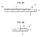
- FIG. 1 is a perspective view of a shelf antenna according to a first embodiment
- FIG. 2A is a side sectional view of the shelf antenna seen from the direction of arrows along the line IIA-IIA in FIG. 1
- FIG. 2B is a side sectional view of the shelf antenna seen from the direction of arrows along the line IIB-IIB in FIG. 1
- FIG. 3 is a plan view of the shelf antenna depicted in FIG. 1 .
- a shelf antenna 1 includes a substrate 10, a ground electrode 11 provided on a lower surface of the substrate 10, a conductor provided on an upper face of the substrate 10, and a plurality of resonators 13-1 to 13-4 provided on the same plane as the conductor 12.
- the substrate 10 supports the ground electrode 11, the conductor 12, and the resonators 13-1 to 13-4.
- the substrate 10 is formed of a dielectric, and therefore the ground electrode 11 is isolated from the conductor 12 and the resonators 13-1 to 13-4.
- the substrate 10 is formed of a glass epoxy resin such as Flame Retardant Type 4 (FR-4).
- FR-4 Flame Retardant Type 4
- the substrate 10 may be formed of another dielectric that may be formed into layer form.
- the thickness of the substrate 10 is determined so that the characteristic impedance of the shelf antenna 1 has a certain or predetermined value, for example, 50 ⁇ or 75 ⁇ .
- the ground electrode 11, the conductor 12, and the resonators 13-1 to 13-4 are formed of metal, such as copper, gold, silver, or nickel, or an alloy thereof, or another electric conductive material.
- the ground electrode 11, the conductor 12, and the resonators 13-1 to 13-4, as illustrated in FIG. 1 , FIGs. 2A and 2B , are fixed onto the lower surface or the upper surface of the substrate 10 by, for example, etching or adhesion.
- the ground electrode 11 is a flat and grounded conductor, and is provided in such a manner as to cover the entire lower surface of the substrate 10.
- the conductor 12 is a linear conductor provided on the upper surface of the substrate 10, and is arranged substantially in parallel with the longitudinal direction of the substrate 10 and at a position at which the substrate 10 is divided substantially in half along the transverse direction thereof, as illustrated in FIG. 1 .
- One end of the conductor 12 serves as a feeding point 12a, and is connected to a communication circuit (not depicted) that processes radio signals radiated or received through the shelf antenna 1.
- the other end 12b of the conductor 12 is an open end.
- the conductor 12, the ground electrode 11, and the substrate 10 together form a microstrip line which functions as a microstrip antenna and is an example of a distribution constant line.
- the end point 12b of the conductor 12 Since the end point 12b of the conductor 12 is an open end, a radio wave radiated from the microstrip antenna, or a radio wave received by the microstrip antenna causes a current flowing through the conductor 12 to form a standing wave. Therefore, nodal points of the standing wave are formed at positions apart from the end point 12b of the conductor 12, that is, from the open end of the microstrip antenna by distances corresponding to integral multiples of a half of the radio wave. Note that since the conductor 12 is arranged on the upper surface of the substrate 10, which is a dielectric, the wavelength of radio waves on the substrate 10 is shorter in accordance with the relative permittivity of the substrate 10 as compared with the wavelength in the air.
- the wavelength of radio waves radiated from a microstrip antenna or received by a microstrip antenna will be referred to as a "design wavelength" hereinafter for the sake of convenience.
- the design wavelength is represented by ⁇ .
- Each of the resonators 13-1 to 13-4 is formed of a loop-shaped conductor that has a length substantially equal to a half of the design wavelength along the longitudinal direction of the resonator and in which the length of one round is substantially equal to the design wavelength, and is provided on the upper surface of the substrate 10.
- the conductor 12 and the resonators 13-1 to 13-4 are provided on the same plane.
- each of the resonators 13-1 to 13-4 is arranged at a position of a distance of substantially an integral multiple of a half of the design wavelength along the conductor 12 from the open end 12b of the conductor 12 so that one end of each resonator is positioned within the range in which one end of the resonator is electromagnetically coupled to the conductor 12.
- each of the resonators 13-1 to 13-4 is electromagnetically coupled to the microstrip antenna with an electric field in the vicinity of a node of the standing wave of a current that is caused to flow through the conductor 12 by the radio wave.
- Each of the resonators 13-1 to 13-4 may therefore radiate or receive a radio wave having the design wavelength.
- the longitudinal directions of the resonators 13-1 to 13-4 are arranged to be orthogonal to the longitudinal direction of the conductor 12.
- Each of the resonators 13-1 to 13-4 may therefore form an electric field that extends in a different direction from an electric field caused by the microstrip antenna.
- the uniformity and the intensity of the electric field in the vicinity of the surface of the shelf antenna 1 are improved as compared to the electric field caused by only the microstrip antenna.
- phase of a current flowing through the microstrip line is reversed between positions located at intervals of a half of the design wavelength on the conductor 12. Therefore, when two resonators are arranged at an interval of a half of the design wavelength on the same side with respect to the width direction of the conductor 12, currents flowing through the two resonators have opposite phases, that is, the directions of the flowing currents are reversed. As a result, electric fields produced by the two resonators cancel out each other. In contrast, when two resonators are arranged at an interval of an integral multiple of the design wavelength on the same side with respect to the width direction of the conductor 12, currents flowing through the two resonators are in phase, that is, the directions of the flowing currents are the same.
- resonators are alternately arranged in such a manner as to sandwich the conductor 12 therebetween. Two adjacent resonators are arranged so that their one ends are positioned within ranges in which electromagnetic coupling to the conductor 12 is possible in the vicinities of two adjacent nodal points of the conductor 12, respectively.
- the interval between ends of two adjacent resonators on the side where the ends are electromagnetically coupled to the conductor 12 is approximately a half of the design wavelength.
- the resonator 13-1 is arranged in the vicinity of a position apart from the open end 12b by a distance of a half of the design wavelength, ⁇ /2.
- the resonator 13-2 is arranged in the vicinity of a position apart from the resonator 13-1 by a distance of ⁇ on the same side as the resonator 13-1.
- the resonators 13-3 and 13-4 are arranged in the vicinities of positions apart from the resonators 13-1 and 13-2 by a distance of ⁇ /2, respectively, on a side of the conductor 12 opposite to the resonators 13-1 and 13-2. That is, the resonators 13-3 and 13-4 are arranged in the vicinities of positions apart from the open end 12b by ⁇ and 2 ⁇ , respectively.
- Each of the resonators 13-1 to 13-4 is formed in the shape of a loop, and has a length of approximately a half of the design wavelength along the longitudinal direction as illustrated in FIG. 3 .
- the current that is caused to flow through each resonator by a radio wave radiated or received by the shelf antenna 1 is an alternating current, and therefore the phase is reversed for each half of the wavelength of the alternating current, that is, the direction of the current is reversed. Therefore, in a resonator formed in a loop shape having a length of approximately a half of the design wavelength along the longitudinal direction, the directions of a current flowing in two portions along the longitudinal direction of that resonator are the same. Therefore, the electric fields produced at the two portions, respectively, may reinforce each other.
- FIG. 4 is a plan view of the shelf antenna 1 illustrating dimensions of elements used for the simulation.
- FIG. 5 is a graph depicting a simulation result of frequency characteristics of an S parameter of the shelf antenna 1.
- FIG. 6 is an illustration depicting a simulation result of an electric field formed in the vicinity of the surface of the shelf antenna 1.
- a relative permittivity ⁇ r of the dielectric forming the substrate 10 is 4.0, and a dielectric loss tangent tan ⁇ of the dielectric is 0.01.
- the substrate 10 has a length along the longitudinal direction of the conductor 12 of 500 mm, and has a length along a direction orthogonal to the longitudinal direction of the conductor 12 of 240 mm.
- the thickness of the substrate 10 is 3 mm.
- the width of the conductor 12 is 6 mm, and the length from the feeding point 12a to the open end 12b is 417 mm.
- the width of a conductor forming each of the resonators 13-1 to 13-4 is 3 mm, and the interval between two lines of the conductor along the longitudinal direction of each resonator is 5 mm. Additionally, the length along the longitudinal direction of each resonator is 85 mm (the interval along the longitudinal direction of the inside of a loop is 79 mm).
- the distance from the open end 12b of the conductor 12 to the resonator 13-1 is 84 mm. Additionally, the interval between the resonator 13-1 and the resonator 13-2 and the interval between the resonator 13-3 and the resonator 13-4 are each 171 mm. The distance from the resonator 13-4 to the feeding point 12a is 40 mm.
- a graph 500 depicts frequency characteristics of the S11 parameter of the shelf antenna 1 obtained by simulation of an electromagnetic field using the finite integration technique. As depicted in the graph 500, it is found that, in the shelf antenna 1, the S11 parameter is at or below -10 dB, which is regarded as an indication of favorable antenna characteristics, at around 930 MHz in the 900 MHz band, which is used in RFID systems.
- a graph 600 depicts the intensity distribution of an electric field of a plane parallel to the surface of the shelf antenna 1 at a position 30 cm above the surface of the shelf antenna 1. Note that the frequency of a radio wave is assumed to be 930 MHz. In the graph 600, where the higher the density is, the stronger the electric field is. As depicted in the graph 600, it is found that the electric field extends uniformly not only a direction along the longitudinal direction of the conductor 12 but also in a direction orthogonal to the longitudinal direction of the conductor 12.
- one end of the microstrip antenna is formed as an open end, and thus the current flowing through the microstrip antenna forms a standing wave.
- one or more resonators are arranged on the same plane as a conductor forming the microstrip line, and thus the microstrip antenna and the resonators are electromagnetically coupled. Therefore, in this shelf antenna, radio waves may be radiated from both the microstrip antenna and each resonator, or may be received by both of them. This may improve the uniformity of an electric field in the vicinity of the surface of the shelf antenna and may increase the intensity of that electric field.
- the resonators and the conductor forming the microstrip line are arranged on the same plane. It is therefore unnecessary to form the substrate in a multiplayer structure. For this reason, this shelf antenna may suppress the manufacturing cost.
- the end point 12b opposite to the feeding point 12a of the conductor 12 may be, for example, shorted through a via formed in the substrate 10 to the ground electrode 11.
- the end point 12b serves as a fixed end for a current flowing through the microstrip line.
- the position of a nodal point of a current flowing through the conductor 12 is identified.
- a position apart from the end point 12b by a distance of (1/4+n/2) ⁇ . (where n is an integer of zero or greater, and ⁇ is the design wavelength) along the longitudinal direction of the conductor 12 is the position of a nodal point.
- All the resonators are alternately arranged in such a manner as to sandwich the conductor 12 therebetween, in order from a position apart from the end point 12b by 1/4 ⁇ along the longitudinal direction of the conductor 12 so that the interval between adjacent resonators is ⁇ /2.
- each resonator is not limited to the loop shape.
- FIG. 7 is a plan view of a shelf antenna 2 according to this modification.
- the shelf antenna 2 differs from the shelf antenna 1 according to the foregoing embodiment only in the shape of a resonator. Accordingly, a resonator will be described below.
- each of resonators 23-1 to 23-4 is a dipole antenna formed in the shape of a hairpin as illustrated in FIG. 7 , and differs in that an end on the side remote from the conductor 12 is opened, from each of the resonator 13-1 to 13-4 depicted in FIG. 1 .
- each of the resonators 23-1 to 23-4 is set to a half of the design wavelength.
- the resonators are alternately arranged in such a manner as to sandwich the conductor 12 therebetween on the upper surface of the substrate 10.
- Two adjacent resonators are arranged so that the interval between ends thereof on the side where these resonators are electromagnetically coupled to the conductor 12 is a half of the design wavelength.
- two adjacent resonators are arranged so that their respective one ends are positioned within ranges in which electromagnetic coupling to the conductor 12 is possible in the vicinities of two adjacent nodal points of the conductor 12, respectively.
- FIG. 8 is a graph depicting a simulation result of frequency characteristics of an S parameter of the shelf antenna 2.
- FIG. 9 is an illustration depicting a simulation result of an electric field formed in the vicinity of the surface of the shelf antenna 2. Note that, in the simulation of FIG. 8 and FIG. 9 , the dimensions and the electric characteristics of each element are assumed to be the same as the dimensions and the electric characteristics of each element in the simulation for the first embodiment.
- a graph 800 depicts frequency characteristics of the S11 parameter of the shelf antenna 2 obtained by simulation of an electromagnetic field using the finite integration technique. As depicted in the graph 800, it is found that, in the shelf antenna 2, the S11 parameter is approximately -10 dB at around 940 MHz.
- a graph 900 depicts the intensity distribution of an electric field of a plane parallel to the surface of the shelf antenna 2 at a position 30 cm above the surface of the shelf antenna 2. Note, however, that the frequency of a radio wave is assumed to be 940 MHz. In the graph 900, where the higher the density is, the stronger the electric field is. As depicted in the graph 900, it is found that the electric field extends uniformly not only a direction along the longitudinal direction of the conductor 12 but also in a direction orthogonal to the longitudinal direction of the conductor 12.
- a resonator may be a dipole antenna having a length of a half of the design wavelength.
- FIG. 10 is a plan view of a shelf antenna 3 according to this modification.
- the shelf antenna 3 differs from the shelf antenna 1 according to the first embodiment only in the shape of a resonator. Accordingly, a resonator will be described below.
- each of resonators 33-1 to 33-4 is a dipole antenna formed of a linear conductor.
- the length in the longitudinal direction of each of the resonators 33-1 to 33-4 is set to a half of the design wavelength.
- the resonators are alternately arranged in such a manner as to sandwich the conductor 12 therebetween on the upper surface of the substrate 10.
- Two adjacent resonators are arranged so that the interval between ends thereof on the side where the resonators are electromagnetically coupled to the conductor 12 is a half of the design wavelength.
- two adjacent resonators are arranged so that their respective one ends are positioned within ranges in which electromagnetic coupling to the conductor 12 is possible in vicinities of two adjacent nodal points of the conductor 12, respectively.
- the interval between each resonator and the conductor 12 forming the microstrip line is preferably narrower than the interval between the resonator according to the first embodiment or the aforementioned modification and the conductor.
- FIG. 11 is a graph depicting a simulation result of frequency characteristics of an S parameter of the shelf antenna 3.
- FIG. 12 is an illustration depicting a simulation result of an electric field formed in the vicinity of the surface of the shelf antenna 3. Note that, in the simulation of FIG. 11 and FIG. 12 , the dimensions and the electric characteristics of each element differ from the dimensions and the electric characteristics of each element in the simulation for the first embodiment only in the dimensions and arrangement of resonators. In this simulation, the width of a conductor forming each of the resonators 33-1 to 33-4 is 15 mm, and the length of each resonator along the longitudinal direction thereof is 83.3 mm.
- the interval between the resonator 33-1 and the resonator 33-2 and the interval between the resonator 33-3 and the resonator 33-4 are each assumed to be 167 mm.
- the distances from the feeding point 12a to the resonators 33-2 and 33-4 are assumed to be 129 mm and 38 mm, respectively.
- the interval between each resonator and the conductor 12 is assumed to be 1.5 mm.
- a graph 1100 depicts frequency characteristics of the S11 parameter of the shelf antenna 3 obtained by simulation of an electromagnetic field using the finite integration technique. As depicted in the graph 1100, it is found that, in the shelf antenna 3, the S11 parameter is at or below -10 dB around 930 MHz.
- a graph 1200 depicts the intensity distribution of an electric field of a plane parallel to the surface of the shelf antenna 3 at a position 30 cm above the surface of the shelf antenna 3. Note, however, that the frequency of a radio wave is assumed to be 940 MHz. In the graph 1200, where the higher the density is, the stronger the electric field is. As depicted in the graph 1200, it is found that the electric field extends uniformly not only a direction along the longitudinal direction of the conductor 12 but also in a direction orthogonal to the longitudinal direction of the conductor 12.
- each resonator may be arranged in a tilted manner so that, as the distance from the conductor 12, which forms the microstrip line, increases, the resonator approaches the feeding point or becomes more distant from the feeding point.
- each resonator may be formed, for example, in the shape of a curve, an arc, or a meandering line.
- the length along the longitudinal direction of each resonator be approximately a half of the design wavelength.
- the shelf antenna according to the second embodiment differs, from the shelf antenna according to the first embodiment, in that resonators are arranged so that an electric field produced is circular polarization. Accordingly, elements related to a resonator will be described below. For other elements of the shelf antenna according to the second embodiment, reference is to be made to description of the corresponding elements of the shelf antenna according to the first embodiment.
- FIG. 13 is a plan view of the shelf antenna according to the second embodiment.
- each of four resonators 43-1 to 43-4 is formed of a loop-shaped conductor having a length of approximately a half of the design wavelength along the longitudinal direction, and is provided on the upper surface of the substrate 10. That is, each of the resonators 43-1 to 43-4 and the conductor 12 are arranged on the same plane.
- the resonator 43-1 and 43-2 are arranged so that the longitudinal directions thereof are substantially parallel with the longitudinal direction of the conductor 12.
- the resonator 43-1 and 43-2 are arranged so as to be substantially orthogonal to the resonators 43-3 and 43-4.
- the resonators 43-1 and 43-2 are further arranged so as to be close to antinode portions of the standing wave of a current flowing through the microstrip line, that is, portions where the magnetic field produced by the current flowing through the microstrip line is maximized.
- One end of the resonator 43-1 and one end of the resonator 43-2 are arranged in the vicinities of nodes of the standing wave of the current flowing through the microstrip line, where the resonators 43-3 and 43-4 are arranged.
- the lengths in the longitudinal directions of the resonators 43-1 and 43-2 are each approximately a half of the design wavelength ⁇ , and the distance from a nodal point of the standing wave to the adjacent antinode is ⁇ /4. Therefore, the neighborhood of the center of the resonators 43-1 and 43-2 is close to the portion of an antinode of the standing wave of the current flowing through the microstrip line.
- the microstrip line and the resonators 43-1 and 43-2 are electromagnetically coupled. Note that the resonator 43-1 and 43-2 are arranged substantially in parallel with the conductor 12.
- the resonators 43-1 and 43-2 arranged substantially in parallel with the conductor 12 only have to be close to antinodes of the standing wave of the current flowing through the conductor 12.
- the position of one end of each of these resonators along the longitudinal direction of the conductor 12 may differ from the position of any resonator arranged to be substantially orthogonal to the conductor 12.
- the interval between an end point of the resonator 43-1 on the side of the feeding point 12a and an end point of the resonator 43-2 on the side of the feeding point 12a is substantially equal to ⁇ so that currents flowing through the resonators 43-1 and 43-2 are in phase.
- the interval between the resonator 43-3 and the resonator 43-4 is substantially equal to ⁇ so that the currents flowing through the resonators 43-3 and 43-4 are in phase.
- the resonators 43-1 and 43-2 cause an electric field substantially parallel with the longitudinal direction of the conductor 12 to be produced, whereas the resonators 43-3 and 43-4 cause an electric field substantially orthogonal to the longitudinal direction of the conductor 12 to be produced.
- the phase of the current at a nodal point of the standing wave shifts from the phase of the current at an antinode adjacent to the nodal point by ⁇ /4.
- the phase of a current flowing through the resonators 43-1 and 43-2 also shifts from the phase of a current flowing through the resonators 43-3 and 43-4 by ⁇ /4.
- FIG. 14 is a plan view of the shelf antenna 4 illustrating dimensions of elements used for the simulation of antenna characteristics of the shelf antenna 4 according to the second embodiment.
- FIG. 15 is a graph depicting a simulation result of frequency characteristics of an S parameter of the shelf antenna 4.
- FIG. 16A to FIG. 16C are illustrations depicting a simulation result of changes in time of the directions of an electric field formed in the vicinity of the surface of the shelf antenna 4. Note that, in this simulation, the dimensions and the electric characteristics of each element differ from the dimensions and the electric characteristics of each element in the first simulation only in the dimensions and arrangement of the resonators 43-1 and 43-2 and the width of the substrate 10. In this simulation, the width of the substrate 10 is 180 mm.
- the lengths in the longitudinal directions of the resonators 43-1 and 43-2 are 87 mm, and the interval between the resonators 43-1 and 43-2 is 95 mm. Additionally, the distance from the feeding point 12a to the resonator 43-1 and the distance from the feeding point 12a to the resonator 43-2 are equal to the distance from the feeding point 12a to the resonator 43-3 and the distance from the feeding point 12a to the resonator 43-4, respectively. Additionally, the intervals between the resonators 43-1 and 43-2 and the conductor 12 is 3 mm, and the interval between the resonators 43-3 and 43-4 and the conductor 12 is 2 mm.
- a graph 1500 depicts frequency characteristics of the S11 parameter of the shelf antenna 4 obtained by simulation of an electromagnetic field using the finite integration technique. As depicted in the graph 1500, it is found that, in the shelf antenna 4, the S11 parameter is at or below -10 dB at around 930 MHz.
- arrows 1601 to 1603 indicate the directions of an electric field at the positions of the arrows at different points in time in a period of time in which the phase of the current varies from 0 to 2 ⁇ at a certain point on the microstrip line. As illustrated in FIG. 16A to FIG. 16C , it is found that the direction of the electric field in each element on the shelf antenna 4 varies with the elapse of time.
- the shelf antenna may make the intensities of an electric field uniform in the vicinity of the surface of the shelf antenna without depending on the directions of the electric field.
- a shelf antenna communicates with another communication device, for example, an RFID tag attached to an article placed on the shelf antenna, there is a possibility that the other communication device may point in various directions with respect to the shelf antenna.
- the shelf antenna may equalize the intensities of an electric field without depending on the directions of the electric field. Therefore, the shelf antenna may achieve satisfactory communication with another communication device without depending on the direction of an antenna of the other communication device.
- the entire shelf antenna may be downsized.
- the end point 12b opposite to the feeding point 12a of the conductor 12 may be, for example, shorted through a via formed in the substrate 10 to the ground electrode 11.
- each resonator is not limited to the loop shape.
- the resonator may be a dipole antenna having a length of a half of the design wavelength.
- FIG. 17 is a plan view of a shelf antenna 5 according to this modification.
- the shelf antenna 5 differs from the shelf antenna 4 according to the aforementioned second embodiment only in the shape of a resonator. Accordingly, a resonator will be described below.
- each of resonators 53-1 to 53-4 is a dipole antenna formed of a linear conductor.
- the length in the longitudinal direction of each of the resonators 53-1 to 53-4 is set to approximately a half of the design wavelength.
- FIG. 18 is a graph depicting a simulation result of frequency characteristics of an S parameter of the shelf antenna 5. Note that, in the simulation of FIG. 18 , the dimensions and the electric characteristics of each element differ from the dimensions and the electric characteristics of each element in the simulation for the second embodiment only in the arrangement of the resonators 53-1 and 53-2. In this simulation, the interval between the resonators 53-1 and 53-2 is 98.7 mm. The distance from the open end 12b of the conductor 12 to the resonator 53-1 is 69.35 mm, and the distance from the feeding point 12a to the resonator 53-2 is 82.35 mm. Additionally, the interval between the resonators 53-1 and 53-2 and the conductor 12 is 3 mm.
- a graph 1800 depicts frequency characteristics of the S11 parameter of the shelf antenna 5 obtained by simulation of an electromagnetic field using the finite integration technique. As depicted in the graph 1800, it is found that, in the shelf antenna 5, the S11 parameter is at or below -10 dB near the range from 930 MHz to 950 MHz.
- FIG. 19 is a plan view of a shelf antenna 6 according to still another modification of the second embodiment.
- the shelf antenna 6 differs from the shelf antenna 4 illustrated in FIG. 13 in the shape of a linear conductor forming a microstrip line and arrangement of resonators.
- a conductor 22, together with a ground electrode (not depicted) provided so as to cover the entire lower surface of the substrate 10, forming a microstrip line is bent zigzag.
- the conductor 22 is bent at right angles.
- each resonator 64 is arranged in the vicinity of a nodal point of the standing wave of a current flowing through the conductor 22 so that electromagnetic coupling to the conductor 22 is possible owing to the electric field.
- each resonator 63 is arranged close to an antinode of the standing wave of the current flowing through the conductor 22 so that electromagnetic coupling to the conductor 22 is possible owing to the current.
- the distance along the conductor 22 between two adjacent resonators 64 is substantially equal to the design wavelength.
- the resonators 63 arranged substantially in parallel with the longitudinal direction of the conductor 22 and the resonators 64 arranged to be substantially orthogonal to the longitudinal direction of the conductor 22 are alternately arranged.
- the shelf antenna 6 since the interval between resonators is shorter than in the second embodiment, the shelf antenna 6 may produce a stronger electric field.
- FIG. 20 is a plan view of a shelf antenna 7 according to yet another modification of each of the foregoing embodiments.
- the shelf antenna 7 differs from the shelf antenna according to each of the foregoing embodiments or modifications in the shape of a linear conductor forming a microstrip line.
- a conductor 32 together with a ground electrode (not depicted) provided so as to cover the lower surface of the substrate 10, forming the microstrip line branches in the course from a feeding point 32a toward the other end into two substantially parallel microstrip lines 32c and 32d.
- An end point of each of the microstrip lines 32c and 32d is an open end or is shorted to a ground electrode provided on the lower surface of the substrate 10, as in each of the foregoing embodiments or modifications.
- each of the microstrip lines 32c and 32d one or more resonators 73 each having a length of approximately a half of the design wavelength are arranged in the vicinities of nodal points of a current flowing through that microstrip line.
- Each of the microstrip lines 32c and 32d and each resonator 73 are electromagnetically coupled, and thus the distribution of electric fields on the surface of the substrate 10 is made uniform and reinforced.
- each resonator 73 may be a conductor formed in the shape of a loop, or may be a dipole antenna.
- the range in which the resonators and the microstrip lines are arranged is broad, and therefore the range in which transmission and reception of radio waves are possible is broader than in the foregoing embodiments or modifications.
- a dielectric layer may be provided over the conductor 12, which forms a microstrip line, and the resonators so that the conductor 12 and the resonators are sandwiched between dielectrics.
- the actual length corresponding to the design wavelength of a radio wave in the conductor 12 and the resonators decreases in accordance with the relative permittivity of each dielectric.
- the entire antenna is more downsized.
- a distribution constant line in another form may be used in place of the microstrip line.
- FIG. 21 is a plan view of a shelf antenna according to a third embodiment.
- a Lecher wire is used as a distribution constant line in place of the microstrip line.
- a Lecher wire 81 and resonators 83-1 to 83-4 are arranged on one surface of the substrate 10 formed of a dielectric. Note that, in this embodiment, since the Lecher wire 81 itself functions as a distribution constant line, a ground electrode does not have to be provided on the other surface of the substrate 10. For this reason, the substrate 10 is used primarily in order to support the Lecher wire 81 and the resonators 83-1 to 83-4.
- the Lecher wire 81 includes two conducting wires 81a and 81b parallel with each other.
- the direction in which a current flows through the conducting wire 81a and the direction in which a current flows through the conducting wire 81b are opposite. Therefore, the resonator 83-1 arranged close to the conducting wire 81a so as to be electromagnetically coupled to the conducting wire 81a and the resonator 83-3 arranged close to the conducting wire 81b so as to be electromagnetically coupled to the conducting wire 81b may be arranged at the same position in the longitudinal direction of the Lecher wire 81. Likewise, the resonator 83-2 and the resonator 83-4 may be arranged at the same position in the longitudinal direction of the Lecher wire 81.
- An end point 81d opposite to a feeding point 81c of the Lecher wire 81 is formed as an open end or is grounded so that the current flowing through the Lecher wire 81 forms a standing wave.
- the resonators 83-1 to 83-4 are each arranged so that one end of each resonator is positioned within a range in which electromagnetic coupling is possible in the vicinity of a node of the standing wave of the current flowing through the Lecher wire 81.
- the resonators 83-1 and 83-2 are arranged in the vicinities of positions apart from the end point 81d by integral multiples of a half of the design wavelength ⁇ .
- each resonator 83-1 and 83-3 are arranged in the vicinities of positions apart from the end point 81d by ⁇ x(1/4+n/2) (where n is an integer of zero or more). Additionally, each resonator is arranged in such a manner that the interval between the resonators 83-1 and 83-3 and the resonators 83-2 and 83-4 is substantially equal to ⁇ so that currents flowing in the resonators 83-1 and 83-4 are in phase. Also in this embodiment, the length in the longitudinal direction of each resonator is preferably approximately a half of the design wavelength.
- FIG. 22 is a plan view of the shelf antenna 8 illustrating dimensions of elements used for the simulation.
- FIG. 23 is a graph depicting a simulation result of frequency characteristics of an S parameter of the shelf antenna 8.
- FIG. 24 is an illustration depicting a simulation result of an electric field formed in the vicinity of the surface of the shelf antenna 8.
- the relative permittivity ⁇ r of a dielectric forming the substrate 10 is 2.2
- the dielectric loss tangent tan ⁇ sigma of the dielectric is 0.00.
- the substrate 10 has a length along the longitudinal direction of the Lecher wire 81 of 800 mm, and has a length along a direction orthogonal to the longitudinal direction of the Lecher wire 81 of 400 mm.
- the thickness of the substrate 10 is 0.6 mm.
- the widths of the conducting wires 81a and 81b of the Lecher wire 81 are each 2 mm, and the interval between the conducting wires is 4 mm.
- the length from the feeding point 81c to the open end 81d is 670 mm.
- the width of a conductor forming each of the resonators 83-1 to 83-4 is 6 mm.
- the length along the longitudinal direction of each resonator is 140.8 mm.
- the distance from the open end 81d to the resonators 83-1 and 83-3 is 146 mm.
- the interval between the resonator 83-1 and the resonator 83-2 and the interval between the resonator 83-3 and the resonator 83-4 are each 292 mm.
- the distance from the resonators 83-2 and 83-4 to the feeding point 81c is 220 mm.
- the interval between each resonator and the Lecher wire 81 is 0.2 mm.
- a graph 2300 depicts frequency characteristics of the S11 parameter of the shelf antenna 8 obtained by simulation of an electromagnetic field using the finite integration technique. As depicted in the graph 2300, it is found that, in the shelf antenna 8, the S11 parameter is at or below -10 dB, which is regarded as an indication of favorable antenna characteristics, at around 920 MHz.
- a graph 2400 depicts the intensity distribution of an electric field of a plane parallel to the surface of the shelf antenna 8 at a position 30 cm above the surface of the shelf antenna 8. Note, however, that the frequency of a radio wave is assumed to be 920 MHz. In the graph 2400, where the higher the density is, the stronger the electric field is. As depicted in the graph 2400, it is found that the electric field extends uniformly not only in a direction along the longitudinal direction of the Lecher wire 81 but also in a direction orthogonal to the longitudinal direction of the Lecher wire 81.
- a ground electrode does not have to be provided on the back of the substrate. Therefore, the thickness of the substrate does not have to be taken into consideration when the characteristic impedance of a shelf antenna is adjusted. For this reason, according to this embodiment, the thickness of a shelf antenna may be more reduced.
- the number of resonators is not limited to the illustrated number, and may be one or more.
Abstract
Description
- The embodiments discussed herein are related to for example, a planar antenna.
- Radio identification (RFID) systems have been widely used in recent years. Typical examples of RFID systems include systems that use electromagnetic waves equivalent to a UHF band (900 MHz band) or microwaves (2.45 GHz) as communication media, and systems that use mutual induction magnetic fields. Among such systems, RFID systems that use electromagnetic waves in the UHF band have attracted much attention because these RFID systems have relatively long distances over which communication is possible.
- As antennas that may be used in order for a tag reader to communicate with radio frequency identification tags using UHF-band electromagnetic waves, microstrip antennas in which a microstrip line is utilized as an antenna have been proposed (see Japanese Laid-open Patent Publication No.
4-287410 2007-306438 - Meanwhile, managing articles placed on a shelf by integrating an antenna of a tag reader into the shelf and performing communication between RFID tags attached to articles placed on the shelf and the tag reader has been proposed..
- Such an antenna integrated into the shelf is called a shelf antenna. The shelf antenna is preferable to form a uniform and strong electric field in the vicinity of the surface of the shelf antenna for radio waves having a specific frequency used for communication so that the shelf antenna may communicate with RFID tags of articles placed anywhere on the shelf in which the shelf antenna is integrated.
- Accordingly, it is an object of the present specification to provide a planar antenna that may improve the uniformity in electric field and increase the electric field intensity in the vicinity of the surface of an antenna.
- According to an aspect of the invention, a planar antenna includes a substrate formed of a dielectric; a distributed constant line formed on a first surface of the substrate, the distributed constant line including a first end to which power is supplied and a second end that is an open end or is grounded; and at least one first resonator arranged on the first surface of the substrate and within a range in which the at least one first resonator is allowed to be electromagnetically coupled to the distributed constant line in a vicinity of any of nodal points of a standing wave of a current that flows through the distributed constant line in response to a radio wave having a certain design wavelength radiated from the distributed constant line or received by the distributed constant line.
-
-
FIG. 1 is a perspective view of a shelf antenna according to a first embodiment; -
FIG. 2A is a side sectional view of the shelf antenna seen from the direction of arrows along the line IIA-IIA inFIG. 1 ; -
FIG. 2B is a side sectional view of the shelf antenna seen from the direction of arrows along the line IIB-IIB inFIG. 1 ; -
FIG. 3 is a plan view of the shelf antenna depicted inFIG. 1 ; -
FIG. 4 is a plan view of the shelf antenna illustrating dimensions of elements used for simulation of antenna characteristics of the shelf antenna according to the first embodiment; -
FIG. 5 is a graph depicting a simulation result of frequency characteristics of an S parameter of the shelf antenna according to the first embodiment; -
FIG. 6 is an illustration depicting a simulation result of an electric field formed in the vicinity of the surface of the shelf antenna according to the first embodiment; -
FIG. 7 is a plan view of a shelf antenna according to a modification of the first embodiment; -
FIG. 8 is a graph depicting a simulation result of frequency characteristics of an S parameter of the shelf antenna according to the modification depicted inFIG. 7 ; -
FIG. 9 is an illustration depicting a simulation result of an electric field formed in the vicinity of the surface of the shelf antenna according to the modification depicted inFIG. 7 ; -
FIG. 10 is a plan view of a shelf antenna according to a further modification of the first embodiment; -
FIG. 11 is a graph depicting a simulation result of frequency characteristics of an S parameter of the shelf antenna according to the modification depicted inFIG. 10 ; -
FIG. 12 is an illustration depicting a simulation result of an electric field formed in the vicinity of the surface of the shelf antenna according to the modification depicted inFIG. 10 ; -
FIG. 13 is a plan view of a shelf antenna according to a second embodiment; -
FIG. 14 is a plan view of the shelf antenna illustrating dimensions of elements used for a simulation of antenna characteristics of the shelf antenna according to the second embodiment; -
FIG. 15 is a graph depicting a simulation result of frequency characteristics of an S parameter of the shelf antenna according to the second embodiment; -
FIG. 16A is an illustration depicting the directions of an electric field in the vicinity of the surface of a shelf antenna at a certain point in time; -
FIG. 16B is an illustration depicting the directions of the electric field in the vicinity of the surface of the shelf antenna at a certain point in time; -
FIG. 16C is an illustration depicting the directions of the electric field in the vicinity of the surface of the shelf antenna at a certain point in time; -
FIG. 17 is a plan view of a shelf antenna according to a modification of the second embodiment; -
FIG. 18 is a graph depicting a simulation result of frequency characteristics of an S parameter of the shelf antenna according to the modification depicted inFIG. 17 ; -
FIG. 19 is a plan view of a shelf antenna according to still another modification of the second embodiment; -
FIG. 20 is a plan view of a shelf antenna according to yet another modification of each embodiment; -
FIG. 21 is a plan view of a shelf antenna according to a third embodiment; -
FIG. 22 is a plan view of the shelf antenna illustrating dimensions of elements used for simulation of antenna characteristics of the shelf antenna according to the third embodiment; -
FIG. 23 is a graph depicting a simulation result of frequency characteristics of an S parameter of the shelf antenna according to the third embodiment; and -
FIG. 24 is an illustration depicting a simulation result of an electric field formed in the vicinity of the surface of the shelf antenna according to the third embodiment. - Hereinafter, a planar antenna will be described according to various embodiments with reference to the accompanying drawings. The planar antenna utilizes, as a microstrip antenna, a microstrip line including an electrical conducting wire or a conducting wire having one end connected to a feeding point and the other end being an open end or being shorted to a ground electrode. Therefore, in the planar antenna, a current flowing through the microstrip antenna is reflected by the other end of the conducting wire, and thereby the current forms a standing wave. At a nodal point of the standing wave, the flowing current is minimized and the intensity of an electric field around the nodal point is maximized. Accordingly, in the planar antenna, at least one resonator is arranged within a range in which the at least one resonator electromagnetically couples to the microstrip antenna in the vicinity of any of nodal points of the standing wave, on the same plane as the conducting wire that forms the microstrip. Thus, the planar antenna may improve the uniformity and the intensity of an electric field in the vicinity of the antenna surface.
- In embodiments described hereinafter, each planar antenna disclosed herein is formed as a shelf antenna. However, each planar antennas disclosed herein may be used for application purposes other than the shelf antenna, for example, as various near-field antennas utilized for communication with RFID tags.
-
FIG. 1 is a perspective view of a shelf antenna according to a first embodiment, andFIG. 2A is a side sectional view of the shelf antenna seen from the direction of arrows along the line IIA-IIA inFIG. 1 .FIG. 2B is a side sectional view of the shelf antenna seen from the direction of arrows along the line IIB-IIB inFIG. 1 .FIG. 3 is a plan view of the shelf antenna depicted inFIG. 1 . - A
shelf antenna 1 includes asubstrate 10, aground electrode 11 provided on a lower surface of thesubstrate 10, a conductor provided on an upper face of thesubstrate 10, and a plurality of resonators 13-1 to 13-4 provided on the same plane as theconductor 12. - The
substrate 10 supports theground electrode 11, theconductor 12, and the resonators 13-1 to 13-4. Thesubstrate 10 is formed of a dielectric, and therefore theground electrode 11 is isolated from theconductor 12 and the resonators 13-1 to 13-4. For example, thesubstrate 10 is formed of a glass epoxy resin such as Flame Retardant Type 4 (FR-4). Alternatively, thesubstrate 10 may be formed of another dielectric that may be formed into layer form. The thickness of thesubstrate 10 is determined so that the characteristic impedance of theshelf antenna 1 has a certain or predetermined value, for example, 50 Ω or 75 Ω. - The
ground electrode 11, theconductor 12, and the resonators 13-1 to 13-4 are formed of metal, such as copper, gold, silver, or nickel, or an alloy thereof, or another electric conductive material. Theground electrode 11, theconductor 12, and the resonators 13-1 to 13-4, as illustrated inFIG. 1 ,FIGs. 2A and 2B , are fixed onto the lower surface or the upper surface of thesubstrate 10 by, for example, etching or adhesion. - The
ground electrode 11 is a flat and grounded conductor, and is provided in such a manner as to cover the entire lower surface of thesubstrate 10. - The
conductor 12 is a linear conductor provided on the upper surface of thesubstrate 10, and is arranged substantially in parallel with the longitudinal direction of thesubstrate 10 and at a position at which thesubstrate 10 is divided substantially in half along the transverse direction thereof, as illustrated inFIG. 1 . One end of theconductor 12 serves as afeeding point 12a, and is connected to a communication circuit (not depicted) that processes radio signals radiated or received through theshelf antenna 1. Theother end 12b of theconductor 12 is an open end. Theconductor 12, theground electrode 11, and thesubstrate 10 together form a microstrip line which functions as a microstrip antenna and is an example of a distribution constant line. - Since the
end point 12b of theconductor 12 is an open end, a radio wave radiated from the microstrip antenna, or a radio wave received by the microstrip antenna causes a current flowing through theconductor 12 to form a standing wave. Therefore, nodal points of the standing wave are formed at positions apart from theend point 12b of theconductor 12, that is, from the open end of the microstrip antenna by distances corresponding to integral multiples of a half of the radio wave. Note that since theconductor 12 is arranged on the upper surface of thesubstrate 10, which is a dielectric, the wavelength of radio waves on thesubstrate 10 is shorter in accordance with the relative permittivity of thesubstrate 10 as compared with the wavelength in the air. At each nodal point of the standing wave, the current is minimized, and a relatively strong electric field is formed around that nodal point. Note that the wavelength of radio waves radiated from a microstrip antenna or received by a microstrip antenna will be referred to as a "design wavelength" hereinafter for the sake of convenience. The design wavelength is represented by λ. - Each of the resonators 13-1 to 13-4 is formed of a loop-shaped conductor that has a length substantially equal to a half of the design wavelength along the longitudinal direction of the resonator and in which the length of one round is substantially equal to the design wavelength, and is provided on the upper surface of the
substrate 10. In other words, theconductor 12 and the resonators 13-1 to 13-4 are provided on the same plane. - As described above, relatively strong electric fields are formed around the
conductor 12 at positions apart from theopen end 12b of the microstrip antenna by distances corresponding to integral multiples of a half of the design wavelength, along theconductor 12. Accordingly, each of the resonators 13-1 to 13-4 is arranged at a position of a distance of substantially an integral multiple of a half of the design wavelength along theconductor 12 from theopen end 12b of theconductor 12 so that one end of each resonator is positioned within the range in which one end of the resonator is electromagnetically coupled to theconductor 12. Thus, for a radio wave having the design wavelength, each of the resonators 13-1 to 13-4 is electromagnetically coupled to the microstrip antenna with an electric field in the vicinity of a node of the standing wave of a current that is caused to flow through theconductor 12 by the radio wave. Each of the resonators 13-1 to 13-4 may therefore radiate or receive a radio wave having the design wavelength. Additionally, the longitudinal directions of the resonators 13-1 to 13-4 are arranged to be orthogonal to the longitudinal direction of theconductor 12. Each of the resonators 13-1 to 13-4 may therefore form an electric field that extends in a different direction from an electric field caused by the microstrip antenna. As a result, the uniformity and the intensity of the electric field in the vicinity of the surface of theshelf antenna 1 are improved as compared to the electric field caused by only the microstrip antenna. - However, the phase of a current flowing through the microstrip line is reversed between positions located at intervals of a half of the design wavelength on the
conductor 12. Therefore, when two resonators are arranged at an interval of a half of the design wavelength on the same side with respect to the width direction of theconductor 12, currents flowing through the two resonators have opposite phases, that is, the directions of the flowing currents are reversed. As a result, electric fields produced by the two resonators cancel out each other. In contrast, when two resonators are arranged at an interval of an integral multiple of the design wavelength on the same side with respect to the width direction of theconductor 12, currents flowing through the two resonators are in phase, that is, the directions of the flowing currents are the same. Likewise, when two resonators are arranged in such a manner as to sandwich theconductor 12 therebetween at intervals of a half of the design wavelength, the directions of currents flowing through the two resonators are also the same. When the directions of currents flowing through two resonators are the same, respective electric fields produced by the resonators reinforce each other. Accordingly, in this embodiment, resonators are alternately arranged in such a manner as to sandwich theconductor 12 therebetween. Two adjacent resonators are arranged so that their one ends are positioned within ranges in which electromagnetic coupling to theconductor 12 is possible in the vicinities of two adjacent nodal points of theconductor 12, respectively. Accordingly, the interval between ends of two adjacent resonators on the side where the ends are electromagnetically coupled to theconductor 12 is approximately a half of the design wavelength. Specifically, the resonator 13-1 is arranged in the vicinity of a position apart from theopen end 12b by a distance of a half of the design wavelength, λ/2. The resonator 13-2 is arranged in the vicinity of a position apart from the resonator 13-1 by a distance of λ on the same side as the resonator 13-1. In contrast, the resonators 13-3 and 13-4 are arranged in the vicinities of positions apart from the resonators 13-1 and 13-2 by a distance of λ/2, respectively, on a side of theconductor 12 opposite to the resonators 13-1 and 13-2. That is, the resonators 13-3 and 13-4 are arranged in the vicinities of positions apart from theopen end 12b by λ and 2λ, respectively. - Each of the resonators 13-1 to 13-4 is formed in the shape of a loop, and has a length of approximately a half of the design wavelength along the longitudinal direction as illustrated in
FIG. 3 . The current that is caused to flow through each resonator by a radio wave radiated or received by theshelf antenna 1 is an alternating current, and therefore the phase is reversed for each half of the wavelength of the alternating current, that is, the direction of the current is reversed. Therefore, in a resonator formed in a loop shape having a length of approximately a half of the design wavelength along the longitudinal direction, the directions of a current flowing in two portions along the longitudinal direction of that resonator are the same. Therefore, the electric fields produced at the two portions, respectively, may reinforce each other. - A simulation result of antenna characteristics of the
shelf antenna 1 will be described below.FIG. 4 is a plan view of theshelf antenna 1 illustrating dimensions of elements used for the simulation.FIG. 5 is a graph depicting a simulation result of frequency characteristics of an S parameter of theshelf antenna 1.FIG. 6 is an illustration depicting a simulation result of an electric field formed in the vicinity of the surface of theshelf antenna 1. In this simulation, a relative permittivity εr of the dielectric forming thesubstrate 10 is 4.0, and a dielectric loss tangent tan δ of the dielectric is 0.01. All of theground electrode 11, theconductor 12, and the resonators 13-1 to 13-4 are formed of copper (conductivity σ=5.8x10⁷ S/m). - As illustrated in
FIG. 4 , thesubstrate 10 has a length along the longitudinal direction of theconductor 12 of 500 mm, and has a length along a direction orthogonal to the longitudinal direction of theconductor 12 of 240 mm. The thickness of thesubstrate 10 is 3 mm. The width of theconductor 12 is 6 mm, and the length from thefeeding point 12a to theopen end 12b is 417 mm. The width of a conductor forming each of the resonators 13-1 to 13-4 is 3 mm, and the interval between two lines of the conductor along the longitudinal direction of each resonator is 5 mm. Additionally, the length along the longitudinal direction of each resonator is 85 mm (the interval along the longitudinal direction of the inside of a loop is 79 mm). The distance from theopen end 12b of theconductor 12 to the resonator 13-1 is 84 mm. Additionally, the interval between the resonator 13-1 and the resonator 13-2 and the interval between the resonator 13-3 and the resonator 13-4 are each 171 mm. The distance from the resonator 13-4 to thefeeding point 12a is 40 mm. - In
FIG. 5 , the horizontal axis represents the frequency [GHz], and the vertical axis represents the value [dB] of an S11 parameter. Agraph 500 depicts frequency characteristics of the S11 parameter of theshelf antenna 1 obtained by simulation of an electromagnetic field using the finite integration technique. As depicted in thegraph 500, it is found that, in theshelf antenna 1, the S11 parameter is at or below -10 dB, which is regarded as an indication of favorable antenna characteristics, at around 930 MHz in the 900 MHz band, which is used in RFID systems. - In
FIG. 6 , agraph 600 depicts the intensity distribution of an electric field of a plane parallel to the surface of theshelf antenna 1 at aposition 30 cm above the surface of theshelf antenna 1. Note that the frequency of a radio wave is assumed to be 930 MHz. In thegraph 600, where the higher the density is, the stronger the electric field is. As depicted in thegraph 600, it is found that the electric field extends uniformly not only a direction along the longitudinal direction of theconductor 12 but also in a direction orthogonal to the longitudinal direction of theconductor 12. - As described above, in this shelf antenna, one end of the microstrip antenna is formed as an open end, and thus the current flowing through the microstrip antenna forms a standing wave. In the vicinity of a nodal point of the standing wave, one or more resonators are arranged on the same plane as a conductor forming the microstrip line, and thus the microstrip antenna and the resonators are electromagnetically coupled. Therefore, in this shelf antenna, radio waves may be radiated from both the microstrip antenna and each resonator, or may be received by both of them. This may improve the uniformity of an electric field in the vicinity of the surface of the shelf antenna and may increase the intensity of that electric field. Additionally, in this shelf antenna, the resonators and the conductor forming the microstrip line are arranged on the same plane. It is therefore unnecessary to form the substrate in a multiplayer structure. For this reason, this shelf antenna may suppress the manufacturing cost.
- Note that, according to a modification, the
end point 12b opposite to thefeeding point 12a of theconductor 12 may be, for example, shorted through a via formed in thesubstrate 10 to theground electrode 11. In this case, theend point 12b serves as a fixed end for a current flowing through the microstrip line. For this reason, using theend point 12b as a fixed end, the position of a nodal point of a current flowing through theconductor 12 is identified. In other words, a position apart from theend point 12b by a distance of (1/4+n/2)λ. (where n is an integer of zero or greater, and λ is the design wavelength) along the longitudinal direction of theconductor 12 is the position of a nodal point. All the resonators are alternately arranged in such a manner as to sandwich theconductor 12 therebetween, in order from a position apart from theend point 12b by 1/4λ along the longitudinal direction of theconductor 12 so that the interval between adjacent resonators is λ/2. - According to another modification, the shape of each resonator is not limited to the loop shape.
FIG. 7 is a plan view of ashelf antenna 2 according to this modification. Theshelf antenna 2 differs from theshelf antenna 1 according to the foregoing embodiment only in the shape of a resonator. Accordingly, a resonator will be described below. In this modification, each of resonators 23-1 to 23-4 is a dipole antenna formed in the shape of a hairpin as illustrated inFIG. 7 , and differs in that an end on the side remote from theconductor 12 is opened, from each of the resonator 13-1 to 13-4 depicted inFIG. 1 . However, also in this example, the length in the longitudinal direction of each of the resonators 23-1 to 23-4 is set to a half of the design wavelength. The resonators are alternately arranged in such a manner as to sandwich theconductor 12 therebetween on the upper surface of thesubstrate 10. Two adjacent resonators are arranged so that the interval between ends thereof on the side where these resonators are electromagnetically coupled to theconductor 12 is a half of the design wavelength. In other words, two adjacent resonators are arranged so that their respective one ends are positioned within ranges in which electromagnetic coupling to theconductor 12 is possible in the vicinities of two adjacent nodal points of theconductor 12, respectively. -
FIG. 8 is a graph depicting a simulation result of frequency characteristics of an S parameter of theshelf antenna 2.FIG. 9 is an illustration depicting a simulation result of an electric field formed in the vicinity of the surface of theshelf antenna 2. Note that, in the simulation ofFIG. 8 and FIG. 9 , the dimensions and the electric characteristics of each element are assumed to be the same as the dimensions and the electric characteristics of each element in the simulation for the first embodiment. - In
FIG. 8 , the horizontal axis represents the frequency [GHz], and the vertical axis represents the value [dB] of an S11 parameter. Agraph 800 depicts frequency characteristics of the S11 parameter of theshelf antenna 2 obtained by simulation of an electromagnetic field using the finite integration technique. As depicted in thegraph 800, it is found that, in theshelf antenna 2, the S11 parameter is approximately -10 dB at around 940 MHz. - In
FIG. 9 , agraph 900 depicts the intensity distribution of an electric field of a plane parallel to the surface of theshelf antenna 2 at aposition 30 cm above the surface of theshelf antenna 2. Note, however, that the frequency of a radio wave is assumed to be 940 MHz. In thegraph 900, where the higher the density is, the stronger the electric field is. As depicted in thegraph 900, it is found that the electric field extends uniformly not only a direction along the longitudinal direction of theconductor 12 but also in a direction orthogonal to the longitudinal direction of theconductor 12. - A resonator may be a dipole antenna having a length of a half of the design wavelength.
FIG. 10 is a plan view of ashelf antenna 3 according to this modification. Theshelf antenna 3 differs from theshelf antenna 1 according to the first embodiment only in the shape of a resonator. Accordingly, a resonator will be described below. In this modification, each of resonators 33-1 to 33-4 is a dipole antenna formed of a linear conductor. However, also in this example, the length in the longitudinal direction of each of the resonators 33-1 to 33-4 is set to a half of the design wavelength. The resonators are alternately arranged in such a manner as to sandwich theconductor 12 therebetween on the upper surface of thesubstrate 10. Two adjacent resonators are arranged so that the interval between ends thereof on the side where the resonators are electromagnetically coupled to theconductor 12 is a half of the design wavelength. In other words, two adjacent resonators are arranged so that their respective one ends are positioned within ranges in which electromagnetic coupling to theconductor 12 is possible in vicinities of two adjacent nodal points of theconductor 12, respectively. In this modification, in order for each of the resonators 33-1 to 33-4 to be electromagnetically coupled to the microstrip line, the interval between each resonator and theconductor 12 forming the microstrip line is preferably narrower than the interval between the resonator according to the first embodiment or the aforementioned modification and the conductor. -
FIG. 11 is a graph depicting a simulation result of frequency characteristics of an S parameter of theshelf antenna 3.FIG. 12 is an illustration depicting a simulation result of an electric field formed in the vicinity of the surface of theshelf antenna 3. Note that, in the simulation ofFIG. 11 and FIG. 12 , the dimensions and the electric characteristics of each element differ from the dimensions and the electric characteristics of each element in the simulation for the first embodiment only in the dimensions and arrangement of resonators. In this simulation, the width of a conductor forming each of the resonators 33-1 to 33-4 is 15 mm, and the length of each resonator along the longitudinal direction thereof is 83.3 mm. Additionally, the interval between the resonator 33-1 and the resonator 33-2 and the interval between the resonator 33-3 and the resonator 33-4 are each assumed to be 167 mm. The distances from thefeeding point 12a to the resonators 33-2 and 33-4 are assumed to be 129 mm and 38 mm, respectively. In addition, the interval between each resonator and theconductor 12 is assumed to be 1.5 mm. - In
FIG. 11 , the horizontal axis represents the frequency [GHz], and the vertical axis represents the value [dB] of an S11 parameter. Agraph 1100 depicts frequency characteristics of the S11 parameter of theshelf antenna 3 obtained by simulation of an electromagnetic field using the finite integration technique. As depicted in thegraph 1100, it is found that, in theshelf antenna 3, the S11 parameter is at or below -10 dB around 930 MHz. - In
FIG. 12 , agraph 1200 depicts the intensity distribution of an electric field of a plane parallel to the surface of theshelf antenna 3 at aposition 30 cm above the surface of theshelf antenna 3. Note, however, that the frequency of a radio wave is assumed to be 940 MHz. In thegraph 1200, where the higher the density is, the stronger the electric field is. As depicted in thegraph 1200, it is found that the electric field extends uniformly not only a direction along the longitudinal direction of theconductor 12 but also in a direction orthogonal to the longitudinal direction of theconductor 12. - Note that, in the foregoing embodiment or modifications, each resonator may be arranged in a tilted manner so that, as the distance from the
conductor 12, which forms the microstrip line, increases, the resonator approaches the feeding point or becomes more distant from the feeding point. Alternatively, each resonator may be formed, for example, in the shape of a curve, an arc, or a meandering line. However, even in the case where each resonator is formed in the shape of a curve, it is preferable that the length along the longitudinal direction of each resonator be approximately a half of the design wavelength. This is because, when the length along the longitudinal direction of a resonator exceeds a half of the design wavelength, there are portions where the directions of a current flowing in the resonator are different, and therefore electric fields produced from the portions with different current directions cancel out each other, thereby weakening the electric fields. - Next, a shelf antenna according to a second embodiment will be described. The shelf antenna according to the second embodiment differs, from the shelf antenna according to the first embodiment, in that resonators are arranged so that an electric field produced is circular polarization. Accordingly, elements related to a resonator will be described below. For other elements of the shelf antenna according to the second embodiment, reference is to be made to description of the corresponding elements of the shelf antenna according to the first embodiment.
-
FIG. 13 is a plan view of the shelf antenna according to the second embodiment. In ashelf antenna 4 according to the second embodiment, each of four resonators 43-1 to 43-4 is formed of a loop-shaped conductor having a length of approximately a half of the design wavelength along the longitudinal direction, and is provided on the upper surface of thesubstrate 10. That is, each of the resonators 43-1 to 43-4 and theconductor 12 are arranged on the same plane. However, unlike theshelf antenna 1 according to the first embodiment, in theshelf antenna 4, the resonator 43-1 and 43-2 are arranged so that the longitudinal directions thereof are substantially parallel with the longitudinal direction of theconductor 12. In other words, the resonator 43-1 and 43-2 are arranged so as to be substantially orthogonal to the resonators 43-3 and 43-4. The resonators 43-1 and 43-2 are further arranged so as to be close to antinode portions of the standing wave of a current flowing through the microstrip line, that is, portions where the magnetic field produced by the current flowing through the microstrip line is maximized. One end of the resonator 43-1 and one end of the resonator 43-2 are arranged in the vicinities of nodes of the standing wave of the current flowing through the microstrip line, where the resonators 43-3 and 43-4 are arranged. The lengths in the longitudinal directions of the resonators 43-1 and 43-2 are each approximately a half of the design wavelength λ, and the distance from a nodal point of the standing wave to the adjacent antinode is λ/4. Therefore, the neighborhood of the center of the resonators 43-1 and 43-2 is close to the portion of an antinode of the standing wave of the current flowing through the microstrip line. Thus, with a current flowing through the microstrip line or a magnetic field produced by the current, the microstrip line and the resonators 43-1 and 43-2 are electromagnetically coupled. Note that the resonator 43-1 and 43-2 are arranged substantially in parallel with theconductor 12. For this reason, even when the interval of the resonators 43-1 and 43-2 and theconductor 12 is larger than the interval of the resonators 43-3 and 43-4 and theconductor 12, it is possible for the resonators 43-1 and 43-2 to be electromagnetically coupled to theconductor 12. - Note that the resonators 43-1 and 43-2 arranged substantially in parallel with the
conductor 12 only have to be close to antinodes of the standing wave of the current flowing through theconductor 12. The position of one end of each of these resonators along the longitudinal direction of theconductor 12 may differ from the position of any resonator arranged to be substantially orthogonal to theconductor 12. - The interval between an end point of the resonator 43-1 on the side of the
feeding point 12a and an end point of the resonator 43-2 on the side of thefeeding point 12a is substantially equal to λ so that currents flowing through the resonators 43-1 and 43-2 are in phase. Likewise, the interval between the resonator 43-3 and the resonator 43-4 is substantially equal to λ so that the currents flowing through the resonators 43-3 and 43-4 are in phase. - As the result of arranging resonators as described above, the resonators 43-1 and 43-2 cause an electric field substantially parallel with the longitudinal direction of the
conductor 12 to be produced, whereas the resonators 43-3 and 43-4 cause an electric field substantially orthogonal to the longitudinal direction of theconductor 12 to be produced. The phase of the current at a nodal point of the standing wave shifts from the phase of the current at an antinode adjacent to the nodal point by π/4. For this reason, the phase of a current flowing through the resonators 43-1 and 43-2 also shifts from the phase of a current flowing through the resonators 43-3 and 43-4 by π/4. The phase of the current flowing through each resonator varies in synchronization, and therefore an electric field produced from the resonator 43-1 and the resonator 43-3 results in circular polarization. Similarly, an electric field produced from the resonator 43-2 and the resonator 43-4 results in circular polarization. For this reason, in the vicinity of the surface of theshelf antenna 4, a combination of the intensities of components of an instantaneous electric field in a direction parallel to the longitudinal direction of theconductor 12 and the intensities of components of the instantaneous electric field in a direction orthogonal to the longitudinal direction of theconductor 12 also varies in response to the change in phase of the current flowing through each resonator. As the result of this, the directions of the instantaneous electric field also vary. For this reason, theshelf antenna 4 may make the intensities of an electric field uniform without depending on the directions of the electric field. - A simulation result of antenna characteristics of the
shelf antenna 4 according to the second embodiment will be described below.FIG. 14 is a plan view of theshelf antenna 4 illustrating dimensions of elements used for the simulation of antenna characteristics of theshelf antenna 4 according to the second embodiment.FIG. 15 is a graph depicting a simulation result of frequency characteristics of an S parameter of theshelf antenna 4.FIG. 16A to FIG. 16C are illustrations depicting a simulation result of changes in time of the directions of an electric field formed in the vicinity of the surface of theshelf antenna 4. Note that, in this simulation, the dimensions and the electric characteristics of each element differ from the dimensions and the electric characteristics of each element in the first simulation only in the dimensions and arrangement of the resonators 43-1 and 43-2 and the width of thesubstrate 10. In this simulation, the width of thesubstrate 10 is 180 mm. Additionally, the lengths in the longitudinal directions of the resonators 43-1 and 43-2 are 87 mm, and the interval between the resonators 43-1 and 43-2 is 95 mm. Additionally, the distance from thefeeding point 12a to the resonator 43-1 and the distance from thefeeding point 12a to the resonator 43-2 are equal to the distance from thefeeding point 12a to the resonator 43-3 and the distance from thefeeding point 12a to the resonator 43-4, respectively. Additionally, the intervals between the resonators 43-1 and 43-2 and theconductor 12 is 3 mm, and the interval between the resonators 43-3 and 43-4 and theconductor 12 is 2 mm. - In
FIG. 15 , the horizontal axis represents the frequency [GHz], and the vertical axis represents the value [dB] of an S11 parameter. Agraph 1500 depicts frequency characteristics of the S11 parameter of theshelf antenna 4 obtained by simulation of an electromagnetic field using the finite integration technique. As depicted in thegraph 1500, it is found that, in theshelf antenna 4, the S11 parameter is at or below -10 dB at around 930 MHz. - In
FIG. 16A to FIG. 16C ,arrows 1601 to 1603 indicate the directions of an electric field at the positions of the arrows at different points in time in a period of time in which the phase of the current varies from 0 to 2π at a certain point on the microstrip line. As illustrated inFIG. 16A to FIG. 16C , it is found that the direction of the electric field in each element on theshelf antenna 4 varies with the elapse of time. - As described above, according to the second embodiment, the shelf antenna may make the intensities of an electric field uniform in the vicinity of the surface of the shelf antenna without depending on the directions of the electric field. When a shelf antenna communicates with another communication device, for example, an RFID tag attached to an article placed on the shelf antenna, there is a possibility that the other communication device may point in various directions with respect to the shelf antenna. However, according to this embodiment, the shelf antenna may equalize the intensities of an electric field without depending on the directions of the electric field. Therefore, the shelf antenna may achieve satisfactory communication with another communication device without depending on the direction of an antenna of the other communication device. In this shelf antenna, resonators on one side with respect to the width direction of a conductor forming the microstrip line are arranged so that the longitudinal direction of the resonators are substantially parallel with the longitudinal direction of the conductor. Therefore, the size of the resonator in a direction orthogonal to the longitudinal direction of the conductor is smaller than in the shelf antenna according to the first embodiment. Thus, the entire shelf antenna may be downsized.
- In the second embodiment, as in the first embodiment, the
end point 12b opposite to thefeeding point 12a of theconductor 12 may be, for example, shorted through a via formed in thesubstrate 10 to theground electrode 11. - According to the second embodiment, the shape of each resonator is not limited to the loop shape. The resonator may be a dipole antenna having a length of a half of the design wavelength.
-
FIG. 17 is a plan view of ashelf antenna 5 according to this modification. Theshelf antenna 5 differs from theshelf antenna 4 according to the aforementioned second embodiment only in the shape of a resonator. Accordingly, a resonator will be described below. - In this modification, each of resonators 53-1 to 53-4 is a dipole antenna formed of a linear conductor. However, also in this example, the length in the longitudinal direction of each of the resonators 53-1 to 53-4 is set to approximately a half of the design wavelength.
-
FIG. 18 is a graph depicting a simulation result of frequency characteristics of an S parameter of theshelf antenna 5. Note that, in the simulation ofFIG. 18 , the dimensions and the electric characteristics of each element differ from the dimensions and the electric characteristics of each element in the simulation for the second embodiment only in the arrangement of the resonators 53-1 and 53-2. In this simulation, the interval between the resonators 53-1 and 53-2 is 98.7 mm. The distance from theopen end 12b of theconductor 12 to the resonator 53-1 is 69.35 mm, and the distance from thefeeding point 12a to the resonator 53-2 is 82.35 mm. Additionally, the interval between the resonators 53-1 and 53-2 and theconductor 12 is 3 mm. - In
FIG. 18 , the horizontal axis represents the frequency [GHz], and the vertical axis represents the value [dB] of an S11 parameter. Agraph 1800 depicts frequency characteristics of the S11 parameter of theshelf antenna 5 obtained by simulation of an electromagnetic field using the finite integration technique. As depicted in thegraph 1800, it is found that, in theshelf antenna 5, the S11 parameter is at or below -10 dB near the range from 930 MHz to 950 MHz. -
FIG. 19 is a plan view of ashelf antenna 6 according to still another modification of the second embodiment. Theshelf antenna 6 differs from theshelf antenna 4 illustrated inFIG. 13 in the shape of a linear conductor forming a microstrip line and arrangement of resonators. - In this modification, a
conductor 22, together with a ground electrode (not depicted) provided so as to cover the entire lower surface of thesubstrate 10, forming a microstrip line is bent zigzag. In this example, each time a pair of aresonator 63 arranged substantially in parallel with the longitudinal direction of theconductor 22 and aresonator 64 arranged substantially orthogonal to the longitudinal direction of theconductor 22, with which a radiated radio wave is circular polarization, is arranged, theconductor 22 is bent at right angles. As in the foregoing second embodiment, eachresonator 64 is arranged in the vicinity of a nodal point of the standing wave of a current flowing through theconductor 22 so that electromagnetic coupling to theconductor 22 is possible owing to the electric field. In contrast, eachresonator 63 is arranged close to an antinode of the standing wave of the current flowing through theconductor 22 so that electromagnetic coupling to theconductor 22 is possible owing to the current. The distance along theconductor 22 between twoadjacent resonators 64 is substantially equal to the design wavelength. However, when tworesonators 64 are arranged apart from each other by the design wavelength on the same side of theconductor 22, currents flowing through the tworesonators 64 that are orthogonal to each other are in phase, and therefore the electric field does not result in circular polarization. To address this, unlike the second embodiment, on the same side with respect to the width direction of theconductor 22, theresonators 63 arranged substantially in parallel with the longitudinal direction of theconductor 22 and theresonators 64 arranged to be substantially orthogonal to the longitudinal direction of theconductor 22 are alternately arranged. - In the
shelf antenna 6 according to this modification, since the interval between resonators is shorter than in the second embodiment, theshelf antenna 6 may produce a stronger electric field. -
FIG. 20 is a plan view of ashelf antenna 7 according to yet another modification of each of the foregoing embodiments. Theshelf antenna 7 differs from the shelf antenna according to each of the foregoing embodiments or modifications in the shape of a linear conductor forming a microstrip line. In this modification, aconductor 32, together with a ground electrode (not depicted) provided so as to cover the lower surface of thesubstrate 10, forming the microstrip line branches in the course from afeeding point 32a toward the other end into two substantiallyparallel microstrip lines microstrip lines substrate 10, as in each of the foregoing embodiments or modifications. Also in this example, for each of themicrostrip lines more resonators 73 each having a length of approximately a half of the design wavelength are arranged in the vicinities of nodal points of a current flowing through that microstrip line. Each of themicrostrip lines resonator 73 are electromagnetically coupled, and thus the distribution of electric fields on the surface of thesubstrate 10 is made uniform and reinforced. Note that eachresonator 73 may be a conductor formed in the shape of a loop, or may be a dipole antenna. In this modification, the range in which the resonators and the microstrip lines are arranged is broad, and therefore the range in which transmission and reception of radio waves are possible is broader than in the foregoing embodiments or modifications. - Note that, in the foregoing embodiment or modification, a dielectric layer may be provided over the
conductor 12, which forms a microstrip line, and the resonators so that theconductor 12 and the resonators are sandwiched between dielectrics. As a result, the actual length corresponding to the design wavelength of a radio wave in theconductor 12 and the resonators decreases in accordance with the relative permittivity of each dielectric. Thus, the entire antenna is more downsized. - According to still another embodiment, a distribution constant line in another form may be used in place of the microstrip line.
-
FIG. 21 is a plan view of a shelf antenna according to a third embodiment. In ashelf antenna 8, a Lecher wire is used as a distribution constant line in place of the microstrip line. In theshelf antenna 8, aLecher wire 81 and resonators 83-1 to 83-4 are arranged on one surface of thesubstrate 10 formed of a dielectric. Note that, in this embodiment, since theLecher wire 81 itself functions as a distribution constant line, a ground electrode does not have to be provided on the other surface of thesubstrate 10. For this reason, thesubstrate 10 is used primarily in order to support theLecher wire 81 and the resonators 83-1 to 83-4. - The
Lecher wire 81 includes two conductingwires conducting wire 81a and the direction in which a current flows through theconducting wire 81b are opposite. Therefore, the resonator 83-1 arranged close to theconducting wire 81a so as to be electromagnetically coupled to theconducting wire 81a and the resonator 83-3 arranged close to theconducting wire 81b so as to be electromagnetically coupled to theconducting wire 81b may be arranged at the same position in the longitudinal direction of theLecher wire 81. Likewise, the resonator 83-2 and the resonator 83-4 may be arranged at the same position in the longitudinal direction of theLecher wire 81. - An
end point 81d opposite to afeeding point 81c of theLecher wire 81 is formed as an open end or is grounded so that the current flowing through theLecher wire 81 forms a standing wave. The resonators 83-1 to 83-4 are each arranged so that one end of each resonator is positioned within a range in which electromagnetic coupling is possible in the vicinity of a node of the standing wave of the current flowing through theLecher wire 81. In other words, when theend point 81d is an open end, the resonators 83-1 and 83-2 are arranged in the vicinities of positions apart from theend point 81d by integral multiples of a half of the design wavelength λ. Otherwise, when theend point 81d is grounded, that is, when theend point 81d is a fixed end, the resonators 83-1 and 83-3 are arranged in the vicinities of positions apart from theend point 81d by λx(1/4+n/2) (where n is an integer of zero or more). Additionally, each resonator is arranged in such a manner that the interval between the resonators 83-1 and 83-3 and the resonators 83-2 and 83-4 is substantially equal to λ so that currents flowing in the resonators 83-1 and 83-4 are in phase. Also in this embodiment, the length in the longitudinal direction of each resonator is preferably approximately a half of the design wavelength. - A simulation result of antenna characteristics of the
shelf antenna 8 will be described below. -
FIG. 22 is a plan view of theshelf antenna 8 illustrating dimensions of elements used for the simulation.FIG. 23 is a graph depicting a simulation result of frequency characteristics of an S parameter of theshelf antenna 8.
FIG. 24 is an illustration depicting a simulation result of an electric field formed in the vicinity of the surface of theshelf antenna 8. In this simulation, the relative permittivity εr of a dielectric forming thesubstrate 10 is 2.2, and the dielectric loss tangent tan δ sigma of the dielectric is 0.00. All theLecher wire 81 and the resonators 83-1 to 83-4 are formed of copper (conductivity σ=5.8x10⁷ S/m). - As illustrated in
FIG. 22 , thesubstrate 10 has a length along the longitudinal direction of theLecher wire 81 of 800 mm, and has a length along a direction orthogonal to the longitudinal direction of theLecher wire 81 of 400 mm. The thickness of thesubstrate 10 is 0.6 mm. - Additionally, the widths of the conducting
wires Lecher wire 81 are each 2 mm, and the interval between the conducting wires is 4 mm. The length from thefeeding point 81c to theopen end 81d is 670 mm. In contrast, the width of a conductor forming each of the resonators 83-1 to 83-4 is 6 mm. Additionally, the length along the longitudinal direction of each resonator is 140.8 mm. The distance from theopen end 81d to the resonators 83-1 and 83-3 is 146 mm. Additionally, the interval between the resonator 83-1 and the resonator 83-2 and the interval between the resonator 83-3 and the resonator 83-4 are each 292 mm. The distance from the resonators 83-2 and 83-4 to thefeeding point 81c is 220 mm. The interval between each resonator and theLecher wire 81 is 0.2 mm. - In
FIG. 23 , the horizontal axis represents the frequency [GHz], and the vertical axis represents the value [dB] of an S11 parameter. Agraph 2300 depicts frequency characteristics of the S11 parameter of theshelf antenna 8 obtained by simulation of an electromagnetic field using the finite integration technique. As depicted in thegraph 2300, it is found that, in theshelf antenna 8, the S11 parameter is at or below -10 dB, which is regarded as an indication of favorable antenna characteristics, at around 920 MHz. - In
FIG. 24 , agraph 2400 depicts the intensity distribution of an electric field of a plane parallel to the surface of theshelf antenna 8 at aposition 30 cm above the surface of theshelf antenna 8. Note, however, that the frequency of a radio wave is assumed to be 920 MHz. In thegraph 2400, where the higher the density is, the stronger the electric field is. As depicted in thegraph 2400, it is found that the electric field extends uniformly not only in a direction along the longitudinal direction of theLecher wire 81 but also in a direction orthogonal to the longitudinal direction of theLecher wire 81. - According to this embodiment, a ground electrode does not have to be provided on the back of the substrate. Therefore, the thickness of the substrate does not have to be taken into consideration when the characteristic impedance of a shelf antenna is adjusted. For this reason, according to this embodiment, the thickness of a shelf antenna may be more reduced.
- Note that, in each of the foregoing embodiments or modifications, the number of resonators is not limited to the illustrated number, and may be one or more.
Claims (9)
- A planar antenna comprising:a substrate formed of a dielectric;a distributed constant line formed on a first surface of the substrate, the distributed constant line including a first end to which power is supplied and a second end that is an open end or is grounded; andat least one first resonator arranged on the first surface of the substrate and within a range in which the at least one first resonator is allowed to be electromagnetically coupled to the distributed constant line in a vicinity of any of nodal points of a standing wave of a current that flows through the distributed constant line in response to a radio wave having a certain design wavelength radiated from the distributed constant line or received by the distributed constant line.
- The planar antenna according to Claim 1, wherein the distributed constant line is a microstrip line including a ground electrode arranged on a second surface of the substrate and a conductor arranged on the first surface of the substrate, the conductor being a linear conductor.
- The planar antenna according to Claim 2, wherein the at least one first resonator includes a plurality of first resonators, the plurality of first resonators being each arranged alternately so as to sandwich the conductor, and two adjacent first resonators of the plurality of first resonators being arranged in a range in which each of the two adjacent first resonators is allowed to be electromagnetically coupled to the distributed constant line, at respective two adjacent nodal points of a current that flows through the conductor.
- The planar antenna according to Claim 1, wherein each of the plurality of first resonators has a length of a half of the design wavelength along a longitudinal direction of the each of the plurality of first resonators.
- The planar antenna according to Claim 2, wherein each of the plurality of first resonators has a length of a half of the design wavelength along a longitudinal direction of the each of the plurality of first resonators.
- The planar antenna according to Claim 3, wherein each of the plurality of first resonators has a length of a half of the design wavelength along a longitudinal direction of the each of the plurality of first resonators.
- The planar antenna according to Claim 2, further comprising:at least one second resonator arranged in parallel with the conductor on the first surface of the substrate and within a range in which at least one second resonator is allowed to be electromagnetic coupled to the conductor in a vicinity of any of antinodes of the standing wave of the current, the at least one second resonator being arranged so as to be orthogonal to the at least one first resonator.
- The planar antenna according to Claim 7, wherein the at least one second resonator includes a plurality of second resonators, and the conductor is formed so that the conductor is bent corresponding to each portion at which a pair of one of the plurality of first resonators and one of the plurality of second resonators is arranged, and the one of plurality of first resonators and the one of plurality second resonators are alternately arranged at an interval of the design wavelength on respective side of the conductor along a longitudinal direction of the conductor.
- The planar antenna according to Claim 1,
wherein the distributed constant line is a Lecher wire including a first conducting wire and a second conducting wire arranged in parallel with each other on the first surface of the substrate, and
wherein the at least one first resonator includes a third resonator arranged so that the third resonator is electromagnetically coupled at one end of the third resonator to the first conducting wire at a nodal point of the first conducting wire located at a certain distance from the second end, and a fourth resonator arranged so that the fourth resonator is electromagnetically coupled at one end of the fourth resonator to the second conducting wire at a nodal point of the second conducting wire located at the certain distance from the second end.
Applications Claiming Priority (1)
| Application Number | Priority Date | Filing Date | Title |
|---|---|---|---|
| JP2013231391A JP6232946B2 (en) | 2013-11-07 | 2013-11-07 | Planar antenna |
Publications (2)
| Publication Number | Publication Date |
|---|---|
| EP2871715A1 true EP2871715A1 (en) | 2015-05-13 |
| EP2871715B1 EP2871715B1 (en) | 2022-09-07 |
Family
ID=51842441
Family Applications (1)
| Application Number | Title | Priority Date | Filing Date |
|---|---|---|---|
| EP14191449.9A Active EP2871715B1 (en) | 2013-11-07 | 2014-11-03 | Planar antenna |
Country Status (4)
| Country | Link |
|---|---|
| US (1) | US9831556B2 (en) |
| EP (1) | EP2871715B1 (en) |
| JP (1) | JP6232946B2 (en) |
| CN (1) | CN104638341B (en) |
Families Citing this family (9)
| Publication number | Priority date | Publication date | Assignee | Title |
|---|---|---|---|---|
| US10312596B2 (en) * | 2013-01-17 | 2019-06-04 | Hrl Laboratories, Llc | Dual-polarization, circularly-polarized, surface-wave-waveguide, artificial-impedance-surface antenna |
| JP6548976B2 (en) * | 2015-06-30 | 2019-07-24 | 富士通株式会社 | Flat antenna |
| JP6891878B2 (en) * | 2016-04-15 | 2021-06-18 | Agc株式会社 | antenna |
| DE102017112348A1 (en) | 2017-06-06 | 2018-12-06 | Dr. Ing. H.C. F. Porsche Aktiengesellschaft | Electric machine |
| DE102018200758A1 (en) * | 2018-01-18 | 2019-07-18 | Robert Bosch Gmbh | Antenna element and antenna array |
| WO2019239976A1 (en) * | 2018-06-11 | 2019-12-19 | コニカミノルタ株式会社 | Contactlessly readable tag, method for manufacturing contactlessly readable tag, identification device, and identification information determination system |
| KR102430247B1 (en) * | 2019-11-21 | 2022-08-09 | 한국전자통신연구원 | Capacitive coupled comb-line microstrip array antenna |
| CN114336003B (en) * | 2020-09-30 | 2024-01-30 | 华为技术有限公司 | Antenna, preparation method thereof, millimeter wave sensor and terminal |
| KR20220100367A (en) * | 2021-01-08 | 2022-07-15 | 한국전자통신연구원 | Capacitive coupled comb-line microstrip array antenna and manufacturing method thereof |
Citations (9)
| Publication number | Priority date | Publication date | Assignee | Title |
|---|---|---|---|---|
| DE2824053A1 (en) * | 1977-05-31 | 1978-12-14 | Emi Ltd | ANTENNA ARRANGEMENT |
| JPS5597703A (en) * | 1978-01-05 | 1980-07-25 | Naohisa Goto | Circularly polarized wave antenna |
| JPS55132107A (en) * | 1979-03-30 | 1980-10-14 | Naoki Inagaki | Microstrip antenna for circular polarized wave |
| EP0289085A2 (en) * | 1987-04-25 | 1988-11-02 | Yoshihiko Sugio | Phase control microstripline antenna |
| US5076655A (en) * | 1990-07-19 | 1991-12-31 | Hughes Aircraft Company | Antenna-fed electro-optic modulator |
| JPH04287410A (en) | 1991-03-16 | 1992-10-13 | Yagi Antenna Co Ltd | Plane antenna |
| US20030063032A1 (en) * | 2001-06-08 | 2003-04-03 | International Business Machines Corporation | Antenna system, transceiver, electrical equipment, and computer terminal |
| JP2007306438A (en) | 2006-05-12 | 2007-11-22 | Toshiba Corp | Antenna apparatus and article management system |
| DE102010040793A1 (en) * | 2010-09-15 | 2012-03-15 | Robert Bosch Gmbh | Group antenna for radar sensors |
Family Cites Families (15)
| Publication number | Priority date | Publication date | Assignee | Title |
|---|---|---|---|---|
| GB1529361A (en) | 1975-02-17 | 1978-10-18 | Secr Defence | Stripline antenna arrays |
| GB2064877B (en) * | 1979-11-22 | 1983-07-27 | Secr Defence | Microstrip antenna |
| JPH0193203A (en) * | 1987-10-03 | 1989-04-12 | Yoshihiko Sugio | Phase controlled microstrip line antenna |
| US5712643A (en) * | 1995-12-05 | 1998-01-27 | Cushcraft Corporation | Planar microstrip Yagi Antenna array |
| KR100322119B1 (en) * | 1998-07-31 | 2002-05-09 | 윤종용 | Planar broadband dipole antenna for linearly polariged waves |
| JP3306592B2 (en) | 1999-05-21 | 2002-07-24 | 株式会社豊田中央研究所 | Microstrip array antenna |
| JP2002271135A (en) | 2001-03-07 | 2002-09-20 | Ueda Japan Radio Co Ltd | Collinear antenna |
| JP3875592B2 (en) * | 2002-04-26 | 2007-01-31 | 日本電波工業株式会社 | Multi-element array type planar antenna |
| US7636064B2 (en) * | 2007-09-05 | 2009-12-22 | Delphi Technologies, Inc. | Dual circularly polarized antenna system and a method of communicating signals by the antenna system |
| JP4743279B2 (en) * | 2009-01-07 | 2011-08-10 | 株式会社デンソー | Microstrip array antenna |
| US20110090130A1 (en) | 2009-10-15 | 2011-04-21 | Electronics And Telecommunications Research Institute | Rfid reader antenna and rfid shelf having the same |
| KR101317183B1 (en) * | 2009-10-15 | 2013-10-15 | 한국전자통신연구원 | RFID Reader Antenna and RFID Shelf including the same |
| US8558748B2 (en) * | 2009-10-19 | 2013-10-15 | Ralink Technology Corp. | Printed dual-band Yagi-Uda antenna and circular polarization antenna |
| JP5636957B2 (en) * | 2010-12-28 | 2014-12-10 | Tdk株式会社 | Wireless communication device |
| JP6470930B2 (en) * | 2014-09-16 | 2019-02-13 | 日本ピラー工業株式会社 | Distributor and planar antenna |
-
2013
- 2013-11-07 JP JP2013231391A patent/JP6232946B2/en active Active
-
2014
- 2014-10-31 US US14/530,217 patent/US9831556B2/en active Active
- 2014-10-31 CN CN201410601676.6A patent/CN104638341B/en active Active
- 2014-11-03 EP EP14191449.9A patent/EP2871715B1/en active Active
Patent Citations (9)
| Publication number | Priority date | Publication date | Assignee | Title |
|---|---|---|---|---|
| DE2824053A1 (en) * | 1977-05-31 | 1978-12-14 | Emi Ltd | ANTENNA ARRANGEMENT |
| JPS5597703A (en) * | 1978-01-05 | 1980-07-25 | Naohisa Goto | Circularly polarized wave antenna |
| JPS55132107A (en) * | 1979-03-30 | 1980-10-14 | Naoki Inagaki | Microstrip antenna for circular polarized wave |
| EP0289085A2 (en) * | 1987-04-25 | 1988-11-02 | Yoshihiko Sugio | Phase control microstripline antenna |
| US5076655A (en) * | 1990-07-19 | 1991-12-31 | Hughes Aircraft Company | Antenna-fed electro-optic modulator |
| JPH04287410A (en) | 1991-03-16 | 1992-10-13 | Yagi Antenna Co Ltd | Plane antenna |
| US20030063032A1 (en) * | 2001-06-08 | 2003-04-03 | International Business Machines Corporation | Antenna system, transceiver, electrical equipment, and computer terminal |
| JP2007306438A (en) | 2006-05-12 | 2007-11-22 | Toshiba Corp | Antenna apparatus and article management system |
| DE102010040793A1 (en) * | 2010-09-15 | 2012-03-15 | Robert Bosch Gmbh | Group antenna for radar sensors |
Also Published As
| Publication number | Publication date |
|---|---|
| CN104638341B (en) | 2018-06-12 |
| JP2015091108A (en) | 2015-05-11 |
| JP6232946B2 (en) | 2017-11-22 |
| US9831556B2 (en) | 2017-11-28 |
| EP2871715B1 (en) | 2022-09-07 |
| CN104638341A (en) | 2015-05-20 |
| US20150123852A1 (en) | 2015-05-07 |
Similar Documents
| Publication | Publication Date | Title |
|---|---|---|
| EP2871715B1 (en) | Planar antenna | |
| JP5018884B2 (en) | Wireless tag and wireless tag manufacturing method | |
| US9059520B2 (en) | Wireless communication device and communication terminal apparatus | |
| US20170077599A1 (en) | Multi-antenna and radio apparatus including thereof | |
| KR101505595B1 (en) | Microstrip chip antenna with top loading structure | |
| US20160301127A1 (en) | Mobile radio device | |
| Cho et al. | Planar near-field RFID reader antenna for item-level tagging | |
| EP2701236A1 (en) | Near field antenna | |
| JP6452477B2 (en) | Antenna and communication device using the same | |
| US11240909B2 (en) | Antenna device | |
| US9819087B2 (en) | Planar antenna | |
| US9590307B2 (en) | Antenna apparatus | |
| JP6233319B2 (en) | Multiband antenna and radio apparatus | |
| JP2011217203A (en) | Planar loop antenna | |
| WO2018163695A1 (en) | Multiband antenna and wireless communication device | |
| JP2011217204A (en) | Planar antenna | |
| KR101008798B1 (en) | U-shaped broadband RFID tag antenna with a parasitic element | |
| JP6395473B2 (en) | Microstrip antenna | |
| JP2016058843A (en) | Planar antenna | |
| EP3295518B1 (en) | Antenna with reversing current elements | |
| JP6574733B2 (en) | Antenna, RFID reader device, RFID reader / writer device, and antenna device | |
| Singh et al. | Tunable microstrip antenna using reactive impedance surface | |
| Svanda et al. | Illustration of the impedance behaviour of extremely low-profile coupled shorted-patches antennas for UHF RFID of people |
Legal Events
| Date | Code | Title | Description |
|---|---|---|---|
| PUAI | Public reference made under article 153(3) epc to a published international application that has entered the european phase |
Free format text: ORIGINAL CODE: 0009012 |
|
| 17P | Request for examination filed |
Effective date: 20141103 |
|
| AK | Designated contracting states |
Kind code of ref document: A1 Designated state(s): AL AT BE BG CH CY CZ DE DK EE ES FI FR GB GR HR HU IE IS IT LI LT LU LV MC MK MT NL NO PL PT RO RS SE SI SK SM TR |
|
| AX | Request for extension of the european patent |
Extension state: BA ME |
|
| R17P | Request for examination filed (corrected) |
Effective date: 20150907 |
|
| RBV | Designated contracting states (corrected) |
Designated state(s): AL AT BE BG CH CY CZ DE DK EE ES FI FR GB GR HR HU IE IS IT LI LT LU LV MC MK MT NL NO PL PT RO RS SE SI SK SM TR |
|
| STAA | Information on the status of an ep patent application or granted ep patent |
Free format text: STATUS: EXAMINATION IS IN PROGRESS |
|
| 17Q | First examination report despatched |
Effective date: 20170927 |
|
| STAA | Information on the status of an ep patent application or granted ep patent |
Free format text: STATUS: EXAMINATION IS IN PROGRESS |
|
| GRAP | Despatch of communication of intention to grant a patent |
Free format text: ORIGINAL CODE: EPIDOSNIGR1 |
|
| STAA | Information on the status of an ep patent application or granted ep patent |
Free format text: STATUS: GRANT OF PATENT IS INTENDED |
|
| INTG | Intention to grant announced |
Effective date: 20220621 |
|
| RIN1 | Information on inventor provided before grant (corrected) |
Inventor name: ANDRENKO, ANDREY S. Inventor name: KAI, MANABU Inventor name: YAMAGAJO, TAKASHI |
|
| GRAS | Grant fee paid |
Free format text: ORIGINAL CODE: EPIDOSNIGR3 |
|
| GRAA | (expected) grant |
Free format text: ORIGINAL CODE: 0009210 |
|
| STAA | Information on the status of an ep patent application or granted ep patent |
Free format text: STATUS: THE PATENT HAS BEEN GRANTED |
|
| AK | Designated contracting states |
Kind code of ref document: B1 Designated state(s): AL AT BE BG CH CY CZ DE DK EE ES FI FR GB GR HR HU IE IS IT LI LT LU LV MC MK MT NL NO PL PT RO RS SE SI SK SM TR |
|
| REG | Reference to a national code |
Ref country code: GB Ref legal event code: FG4D |
|
| REG | Reference to a national code |
Ref country code: CH Ref legal event code: EP Ref country code: AT Ref legal event code: REF Ref document number: 1517828 Country of ref document: AT Kind code of ref document: T Effective date: 20220915 |
|
| REG | Reference to a national code |
Ref country code: DE Ref legal event code: R096 Ref document number: 602014084856 Country of ref document: DE |
|
| REG | Reference to a national code |
Ref country code: IE Ref legal event code: FG4D |
|
| PGFP | Annual fee paid to national office [announced via postgrant information from national office to epo] |
Ref country code: GB Payment date: 20220907 Year of fee payment: 9 |
|
| PGFP | Annual fee paid to national office [announced via postgrant information from national office to epo] |
Ref country code: FR Payment date: 20220901 Year of fee payment: 9 |
|
| REG | Reference to a national code |
Ref country code: LT Ref legal event code: MG9D |
|
| REG | Reference to a national code |
Ref country code: NL Ref legal event code: MP Effective date: 20220907 |
|
| PG25 | Lapsed in a contracting state [announced via postgrant information from national office to epo] |
Ref country code: SE Free format text: LAPSE BECAUSE OF FAILURE TO SUBMIT A TRANSLATION OF THE DESCRIPTION OR TO PAY THE FEE WITHIN THE PRESCRIBED TIME-LIMIT Effective date: 20220907 Ref country code: RS Free format text: LAPSE BECAUSE OF FAILURE TO SUBMIT A TRANSLATION OF THE DESCRIPTION OR TO PAY THE FEE WITHIN THE PRESCRIBED TIME-LIMIT Effective date: 20220907 Ref country code: NO Free format text: LAPSE BECAUSE OF FAILURE TO SUBMIT A TRANSLATION OF THE DESCRIPTION OR TO PAY THE FEE WITHIN THE PRESCRIBED TIME-LIMIT Effective date: 20221207 Ref country code: LV Free format text: LAPSE BECAUSE OF FAILURE TO SUBMIT A TRANSLATION OF THE DESCRIPTION OR TO PAY THE FEE WITHIN THE PRESCRIBED TIME-LIMIT Effective date: 20220907 Ref country code: LT Free format text: LAPSE BECAUSE OF FAILURE TO SUBMIT A TRANSLATION OF THE DESCRIPTION OR TO PAY THE FEE WITHIN THE PRESCRIBED TIME-LIMIT Effective date: 20220907 Ref country code: FI Free format text: LAPSE BECAUSE OF FAILURE TO SUBMIT A TRANSLATION OF THE DESCRIPTION OR TO PAY THE FEE WITHIN THE PRESCRIBED TIME-LIMIT Effective date: 20220907 Ref country code: ES Free format text: LAPSE BECAUSE OF FAILURE TO SUBMIT A TRANSLATION OF THE DESCRIPTION OR TO PAY THE FEE WITHIN THE PRESCRIBED TIME-LIMIT Effective date: 20220907 |
|
| PGFP | Annual fee paid to national office [announced via postgrant information from national office to epo] |
Ref country code: DE Payment date: 20220829 Year of fee payment: 9 |
|
| REG | Reference to a national code |
Ref country code: AT Ref legal event code: MK05 Ref document number: 1517828 Country of ref document: AT Kind code of ref document: T Effective date: 20220907 |
|
| PG25 | Lapsed in a contracting state [announced via postgrant information from national office to epo] |
Ref country code: HR Free format text: LAPSE BECAUSE OF FAILURE TO SUBMIT A TRANSLATION OF THE DESCRIPTION OR TO PAY THE FEE WITHIN THE PRESCRIBED TIME-LIMIT Effective date: 20220907 Ref country code: GR Free format text: LAPSE BECAUSE OF FAILURE TO SUBMIT A TRANSLATION OF THE DESCRIPTION OR TO PAY THE FEE WITHIN THE PRESCRIBED TIME-LIMIT Effective date: 20221208 |
|
| PG25 | Lapsed in a contracting state [announced via postgrant information from national office to epo] |
Ref country code: SM Free format text: LAPSE BECAUSE OF FAILURE TO SUBMIT A TRANSLATION OF THE DESCRIPTION OR TO PAY THE FEE WITHIN THE PRESCRIBED TIME-LIMIT Effective date: 20220907 Ref country code: RO Free format text: LAPSE BECAUSE OF FAILURE TO SUBMIT A TRANSLATION OF THE DESCRIPTION OR TO PAY THE FEE WITHIN THE PRESCRIBED TIME-LIMIT Effective date: 20220907 Ref country code: PT Free format text: LAPSE BECAUSE OF FAILURE TO SUBMIT A TRANSLATION OF THE DESCRIPTION OR TO PAY THE FEE WITHIN THE PRESCRIBED TIME-LIMIT Effective date: 20230109 Ref country code: CZ Free format text: LAPSE BECAUSE OF FAILURE TO SUBMIT A TRANSLATION OF THE DESCRIPTION OR TO PAY THE FEE WITHIN THE PRESCRIBED TIME-LIMIT Effective date: 20220907 Ref country code: AT Free format text: LAPSE BECAUSE OF FAILURE TO SUBMIT A TRANSLATION OF THE DESCRIPTION OR TO PAY THE FEE WITHIN THE PRESCRIBED TIME-LIMIT Effective date: 20220907 |
|
| PG25 | Lapsed in a contracting state [announced via postgrant information from national office to epo] |
Ref country code: SK Free format text: LAPSE BECAUSE OF FAILURE TO SUBMIT A TRANSLATION OF THE DESCRIPTION OR TO PAY THE FEE WITHIN THE PRESCRIBED TIME-LIMIT Effective date: 20220907 Ref country code: PL Free format text: LAPSE BECAUSE OF FAILURE TO SUBMIT A TRANSLATION OF THE DESCRIPTION OR TO PAY THE FEE WITHIN THE PRESCRIBED TIME-LIMIT Effective date: 20220907 Ref country code: IS Free format text: LAPSE BECAUSE OF FAILURE TO SUBMIT A TRANSLATION OF THE DESCRIPTION OR TO PAY THE FEE WITHIN THE PRESCRIBED TIME-LIMIT Effective date: 20230107 Ref country code: EE Free format text: LAPSE BECAUSE OF FAILURE TO SUBMIT A TRANSLATION OF THE DESCRIPTION OR TO PAY THE FEE WITHIN THE PRESCRIBED TIME-LIMIT Effective date: 20220907 |
|
| REG | Reference to a national code |
Ref country code: DE Ref legal event code: R097 Ref document number: 602014084856 Country of ref document: DE |
|
| PG25 | Lapsed in a contracting state [announced via postgrant information from national office to epo] |
Ref country code: NL Free format text: LAPSE BECAUSE OF FAILURE TO SUBMIT A TRANSLATION OF THE DESCRIPTION OR TO PAY THE FEE WITHIN THE PRESCRIBED TIME-LIMIT Effective date: 20220907 Ref country code: MC Free format text: LAPSE BECAUSE OF FAILURE TO SUBMIT A TRANSLATION OF THE DESCRIPTION OR TO PAY THE FEE WITHIN THE PRESCRIBED TIME-LIMIT Effective date: 20220907 Ref country code: AL Free format text: LAPSE BECAUSE OF FAILURE TO SUBMIT A TRANSLATION OF THE DESCRIPTION OR TO PAY THE FEE WITHIN THE PRESCRIBED TIME-LIMIT Effective date: 20220907 |
|
| REG | Reference to a national code |
Ref country code: CH Ref legal event code: PL |
|
| PLBE | No opposition filed within time limit |
Free format text: ORIGINAL CODE: 0009261 |
|
| STAA | Information on the status of an ep patent application or granted ep patent |
Free format text: STATUS: NO OPPOSITION FILED WITHIN TIME LIMIT |
|
| REG | Reference to a national code |
Ref country code: BE Ref legal event code: MM Effective date: 20221130 |
|
| PG25 | Lapsed in a contracting state [announced via postgrant information from national office to epo] |
Ref country code: LI Free format text: LAPSE BECAUSE OF NON-PAYMENT OF DUE FEES Effective date: 20221130 Ref country code: DK Free format text: LAPSE BECAUSE OF FAILURE TO SUBMIT A TRANSLATION OF THE DESCRIPTION OR TO PAY THE FEE WITHIN THE PRESCRIBED TIME-LIMIT Effective date: 20220907 Ref country code: CH Free format text: LAPSE BECAUSE OF NON-PAYMENT OF DUE FEES Effective date: 20221130 |
|
| 26N | No opposition filed |
Effective date: 20230608 |
|
| PG25 | Lapsed in a contracting state [announced via postgrant information from national office to epo] |
Ref country code: SI Free format text: LAPSE BECAUSE OF FAILURE TO SUBMIT A TRANSLATION OF THE DESCRIPTION OR TO PAY THE FEE WITHIN THE PRESCRIBED TIME-LIMIT Effective date: 20220907 Ref country code: LU Free format text: LAPSE BECAUSE OF NON-PAYMENT OF DUE FEES Effective date: 20221103 |
|
| PG25 | Lapsed in a contracting state [announced via postgrant information from national office to epo] |
Ref country code: IE Free format text: LAPSE BECAUSE OF NON-PAYMENT OF DUE FEES Effective date: 20221103 |
|
| PG25 | Lapsed in a contracting state [announced via postgrant information from national office to epo] |
Ref country code: BE Free format text: LAPSE BECAUSE OF NON-PAYMENT OF DUE FEES Effective date: 20221130 |
|
| PG25 | Lapsed in a contracting state [announced via postgrant information from national office to epo] |
Ref country code: HU Free format text: LAPSE BECAUSE OF FAILURE TO SUBMIT A TRANSLATION OF THE DESCRIPTION OR TO PAY THE FEE WITHIN THE PRESCRIBED TIME-LIMIT; INVALID AB INITIO Effective date: 20141103 |