US9819087B2 - Planar antenna - Google Patents
Planar antenna Download PDFInfo
- Publication number
- US9819087B2 US9819087B2 US15/170,695 US201615170695A US9819087B2 US 9819087 B2 US9819087 B2 US 9819087B2 US 201615170695 A US201615170695 A US 201615170695A US 9819087 B2 US9819087 B2 US 9819087B2
- Authority
- US
- United States
- Prior art keywords
- conductor
- resonators
- resonator
- predetermined wavelength
- conductors
- Prior art date
- Legal status (The legal status is an assumption and is not a legal conclusion. Google has not performed a legal analysis and makes no representation as to the accuracy of the status listed.)
- Active
Links
Images


Classifications
-
- H—ELECTRICITY
- H01—ELECTRIC ELEMENTS
- H01Q—ANTENNAS, i.e. RADIO AERIALS
- H01Q9/00—Electrically-short antennas having dimensions not more than twice the operating wavelength and consisting of conductive active radiating elements
- H01Q9/04—Resonant antennas
- H01Q9/0407—Substantially flat resonant element parallel to ground plane, e.g. patch antenna
-
- H—ELECTRICITY
- H01—ELECTRIC ELEMENTS
- H01Q—ANTENNAS, i.e. RADIO AERIALS
- H01Q21/00—Antenna arrays or systems
- H01Q21/0006—Particular feeding systems
- H01Q21/0075—Stripline fed arrays
-
- H—ELECTRICITY
- H01—ELECTRIC ELEMENTS
- H01Q—ANTENNAS, i.e. RADIO AERIALS
- H01Q21/00—Antenna arrays or systems
- H01Q21/24—Combinations of antenna units polarised in different directions for transmitting or receiving circularly and elliptically polarised waves or waves linearly polarised in any direction
-
- H—ELECTRICITY
- H01—ELECTRIC ELEMENTS
- H01Q—ANTENNAS, i.e. RADIO AERIALS
- H01Q9/00—Electrically-short antennas having dimensions not more than twice the operating wavelength and consisting of conductive active radiating elements
- H01Q9/04—Resonant antennas
- H01Q9/0407—Substantially flat resonant element parallel to ground plane, e.g. patch antenna
- H01Q9/045—Substantially flat resonant element parallel to ground plane, e.g. patch antenna with particular feeding means
- H01Q9/0457—Substantially flat resonant element parallel to ground plane, e.g. patch antenna with particular feeding means electromagnetically coupled to the feed line
-
- H—ELECTRICITY
- H01—ELECTRIC ELEMENTS
- H01Q—ANTENNAS, i.e. RADIO AERIALS
- H01Q9/00—Electrically-short antennas having dimensions not more than twice the operating wavelength and consisting of conductive active radiating elements
- H01Q9/04—Resonant antennas
- H01Q9/16—Resonant antennas with feed intermediate between the extremities of the antenna, e.g. centre-fed dipole
- H01Q9/28—Conical, cylindrical, cage, strip, gauze, or like elements having an extended radiating surface; Elements comprising two conical surfaces having collinear axes and adjacent apices and fed by two-conductor transmission lines
- H01Q9/285—Planar dipole
-
- H—ELECTRICITY
- H01—ELECTRIC ELEMENTS
- H01Q—ANTENNAS, i.e. RADIO AERIALS
- H01Q1/00—Details of, or arrangements associated with, antennas
- H01Q1/12—Supports; Mounting means
- H01Q1/22—Supports; Mounting means by structural association with other equipment or articles
- H01Q1/2208—Supports; Mounting means by structural association with other equipment or articles associated with components used in interrogation type services, i.e. in systems for information exchange between an interrogator/reader and a tag/transponder, e.g. in Radio Frequency Identification [RFID] systems
- H01Q1/2216—Supports; Mounting means by structural association with other equipment or articles associated with components used in interrogation type services, i.e. in systems for information exchange between an interrogator/reader and a tag/transponder, e.g. in Radio Frequency Identification [RFID] systems used in interrogator/reader equipment
-
- H—ELECTRICITY
- H01—ELECTRIC ELEMENTS
- H01Q—ANTENNAS, i.e. RADIO AERIALS
- H01Q1/00—Details of, or arrangements associated with, antennas
- H01Q1/36—Structural form of radiating elements, e.g. cone, spiral, umbrella; Particular materials used therewith
- H01Q1/38—Structural form of radiating elements, e.g. cone, spiral, umbrella; Particular materials used therewith formed by a conductive layer on an insulating support
Definitions
- a multilayered transmission line plate is disclosed, for example, in Japanese Laid-open Patent Publication No. 2014-090291 includes a multilayered plate formed by stacking a first conductive layer, a first dielectric layer, a second conductive layer, a second dielectric layer, and a third conductive layer, one on top of the other in this order, wherein the second conductive layer forms a microstrip line which functions as a feed line.
- One or more patch conductors are formed on the third conductive layer, and the third conductive layer with such patch conductors formed thereon is disposed so as to partially overlap the second conductive layer when the plane of the multilayered plate is viewed from the top.
- RFID radio frequency identification
- the antenna is configured so as to be able to form a uniform and strong electric field near the surface of the antenna for radio waves having a specific frequency used for the communication.
- a planar antenna includes: a substrate which is formed from a dielectric material; a ground electrode which is provided on one surface of the substrate; a first conductor which is provided on the other surface of the substrate, and which forms a microstrip line in combination with the ground electrode; a second conductor which is provided on the other surface of the substrate so as to extend in parallel to the first conductor, and which forms a microstrip line in combination with the ground electrode; a plurality of first resonators disposed between the first conductor and the second conductor which electromagnetically couple the first conductor at one longitudinal end of each of the first resonators to generate, with a current having a predetermined wavelength and flowing through the first conductor, electric fields which are in phase with each other; and at least one second resonator disposed between the first conductor and the second conductor which electromagnetically couples the second conductor at one longitudinal end of the at least one second resonator to generate, with a current having the predetermined wavelength and flowing through the second
- FIG. 1 is a plan view of a shelf antenna according to a first embodiment.
- FIG. 2A is a cross-sectional side view of the shelf antenna taken along line AA′ in FIG. 1 and viewed in the direction of the arrow.
- FIG. 2B is a cross-sectional side view of the shelf antenna taken along line BB′ in FIG. 1 and viewed in the direction of the arrow.
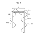
- FIG. 3 is a schematic diagram illustrating the phase of current flowing through conductors.
- FIG. 4 is a plan view illustrating the dimensions of the various parts of the shelf antenna according to the first embodiment used in simulation.
- FIG. 5 is a diagram depicting a simulation result of the frequency characteristic of an S-parameter of the shelf antenna according to the first embodiment.
- FIG. 6 is a diagram depicting a simulation result of the axial ratio of an electric field formed by the shelf antenna according to the first embodiment.
- FIG. 7A is a diagram depicting a simulation result of the intensity distribution of a direction component of the electric field in an x-y plane elevated 2 mm above the surface of a substrate along the z axis.
- FIG. 7B is a diagram depicting a simulation result of the intensity distribution of a direction component of the electric field in the x-y plane elevated 2 mm above the surface of the substrate along the z axis.
- FIG. 7C is a diagram depicting a simulation result of the intensity distribution of a direction component of the electric field in the x-y plane elevated 2 mm above the surface of the substrate along the z axis.
- FIG. 7D is a diagram depicting a simulation result of the intensity distribution of a direction component of the electric field in the x-y plane elevated 7 mm above the surface of the substrate along the z axis.
- FIG. 7E is a diagram depicting a simulation result of the intensity distribution of a direction component of the electric field in the x-y plane elevated 7 mm above the surface of the substrate along the z axis.
- FIG. 7F is a diagram depicting a simulation result of the intensity distribution of a direction component of the electric field in the x-y plane elevated 7 mm above the surface of the substrate along the z axis.
- FIG. 8A is a diagram depicting a simulation result of the intensity distribution of a direction component of the electric field in the x-y plane elevated 30 mm above the surface of the substrate along the z axis.
- FIG. 8B is a diagram depicting a simulation result of the intensity distribution of a direction component of the electric field in the x-y plane elevated 30 mm above the surface of the substrate along the z axis.
- FIG. 8C is a diagram depicting a simulation result of the intensity distribution of a direction component of the electric field in the x-y plane elevated 30 mm above the surface of the substrate along the z axis.
- FIG. 9A is a diagram depicting an x-z plane defined to examine the intensity distribution of the electric field.
- FIG. 9B is a diagram depicting a simulation result of the intensity distribution of a direction component of the electric field in the x-z plane.
- FIG. 9C is a diagram depicting a simulation result of the intensity distribution of a direction component of the electric field in the x-z plane.
- FIG. 9D is a diagram depicting a simulation result of the intensity distribution of a direction component of the electric field in the x-z plane.
- FIG. 10A is a diagram depicting a y-z plane defined to examine the intensity distribution of the electric field.
- FIG. 10B is a diagram depicting a simulation result of the intensity distribution of a direction component of the electric field in the y-z plane.
- FIG. 10C is a diagram depicting a simulation result of the intensity distribution of a direction component of the electric field in the y-z plane.
- FIG. 10D is a diagram depicting a simulation result of the intensity distribution of a direction component of the electric field in the y-z plane.
- FIG. 11 is a plan view of a shelf antenna according to a second embodiment.
- FIG. 12A is a diagram depicting a simulation result of the intensity distribution of a direction component of the electric field formed near the surface of the shelf antenna according to the second embodiment.
- FIG. 12B is a diagram depicting a simulation result of the intensity distribution of a direction component of the electric field formed near the surface of the shelf antenna according to the second embodiment.
- FIG. 13A is a diagram depicting a simulation result of the intensity distribution of a direction component of the electric field formed in a plane elevated 30 mm above the surface of the substrate according to the second embodiment.
- FIG. 13B is a diagram depicting a simulation result of the intensity distribution of a direction component of the electric field formed in the plane elevated 30 mm above the surface of the substrate according to the second embodiment.
- FIG. 14 is a plan view of a shelf antenna according to a modified example.
- FIG. 15 is a plan view of a shelf antenna according to a further modified example.
- FIG. 16A is a plan view of a shelf antenna according to a still further modified example.
- FIG. 16B is a cross-sectional side view taken along line CC′ in FIG. 16A and viewed in the direction of arrow.
- the planar antenna described herein includes two parallelly arranged line conductors each of which forms a microstrip line in combination with a ground electrode.
- One of the two conductors is fed at one end thereof, and is connected at the other end to one end of the other conductor by a connecting conductor having a length equal to an integral multiple of the wavelength of a current corresponding to the radio wave that the planar antenna radiates or receives.
- a plurality of resonators each of which is disposed with its longitudinal direction crossing an associated one of the conductors is arranged, and each of which resonates with the associated conductor by electromagnetically coupling the conductor and thereby excites a current having the same wavelength as that of the current flowing through the conductor.
- the resonators that electromagnetically couple the same conductor are arranged, one spaced apart from another along the conductor by a distance approximately equal to the wavelength of the current flowing through the conductor. Further, the resonators that electromagnetically couple one of the conductors are displaced in position along the conductor with respect to the respective resonators that electromagnetically couple the other conductor by an amount approximately equal to one half of the current flowing through each conductor. More specifically, the resonators that electromagnetically couple one of the conductors and the resonators that electromagnetically couple the other conductor are arranged in alternating and staggered fashion, one spaced apart from another by a distance approximately equal to one half of the wavelength of the current flowing through each conductor. With this structure, the planar antenna improves the uniformity and strength of the electric field near the planar antenna by reducing the spacing between each resonator while maintaining the current flowing between each resonator in phase.
- each planar antenna disclosed in this specification is configured, for example, as a shelf antenna which is incorporated in a shelf and which is used to communicate with RFID tags attached to the articles placed on the shelf.
- the planar antennas disclosed in this specification may be used for other purposes than shelf antennas.
- the planar antennas disclosed in this patent specification need not be limited in use to RFID tag communication, but may be used as various kinds of near-field antennas to be used for communication with other communication devices.
- FIG. 1 is a plan view of a shelf antenna according to a first embodiment
- FIG. 2A is a cross-sectional side view of the shelf antenna taken along line AA′ in FIG. 1 and viewed in the direction of the arrow
- FIG. 2B is a cross-sectional side view of the shelf antenna taken along line BB′ in FIG. 1 and viewed in the direction of the arrow.
- the shelf antenna 1 includes a substrate 10 , a ground electrode 11 provided on one surface of the substrate 10 , line conductors 12 - 1 to 12 - 3 provided on the other surface of the substrate 10 , and a plurality of resonators 13 - 1 to 13 - 8 formed in the same plane as the line conductors 12 - 1 to 12 - 3 .
- the surface of the substrate 10 on which the ground electrode 11 is formed will hereinafter be referred to as the lower surface or the back surface, while the surface of the substrate 10 on which the conductors 12 and the plurality of resonators 13 - 1 to 13 - 8 are formed will be referred to as the upper surface or the front surface.
- the substrate 10 has a planar shape, and supports the ground electrode 11 , the conductors 12 - 1 to 12 - 3 , and the resonators 13 - 1 to 13 - 8 .
- the substrate 10 is formed from a dielectric material, so that the ground electrode 11 is insulated from the conductors 12 - 1 to 12 - 3 and the resonators 13 - 1 to 13 - 8 .
- the substrate 10 is formed, for example, from a glass epoxy resin such as FR-4. Alternatively, the substrate 10 may be formed from some other dielectric material that can be formed in a layered structure. Further, the thickness of the substrate 10 is chosen so that the characteristic impedance of the shelf antenna 1 becomes equal to a predetermined value, for example, 50 ⁇ or 75 ⁇ .
- the ground electrode 11 , the conductors 12 - 1 to 12 - 3 , and the resonators 13 - 1 to 13 - 8 are each formed, for example, from a metal such as copper, gold, silver, or nickel or an alloy thereof or from some other suitable conductive material. Then, the ground electrode 11 , the conductors 12 - 1 to 12 - 3 , and the resonators 13 - 1 to 13 - 8 are fixed to the back surface or front surface of the substrate 10 , for example, by etching or by adhesive.
- the ground electrode 11 is a grounded planar conductor, and is formed, for example, so as to cover the entire back surface of the substrate 10 .
- the conductors 12 - 1 to 12 - 3 are line conductors formed on the front surface of the substrate 10 .
- the conductors 12 - 1 and 12 - 2 are arranged parallel to each other along the longitudinal direction of the substrate 10 . Further, the conductors 12 - 1 and 12 - 2 are spaced from each other by a distance longer than one half of the design wavelength so that the resonators 13 - 1 to 13 - 4 can be disposed therebetween.
- One end of the conductor 12 - 1 is a feed point 12 a at which the conductor 12 - 1 is connected to a communication circuit (not depicted) which processes radio frequency signals received or to be radiated via the shelf antenna 1 .
- the other end of the conductor 12 - 1 is connected to one end of the conductor 12 - 3 .
- the other end of the conductor 12 - 3 is connected to one end of the conductor 12 - 2 , the one end being the end nearer to the other end of the conductor 12 - 1 .
- the one end of the conductor 12 - 2 is located at the same position as the other end of the conductor 12 - 1 when viewed across the longitudinal direction of the substrate 10 .
- the other end of the conductor 12 - 2 i.e., the end point 12 b nearer to the feed point 12 a, is an open end.
- the conductors 12 - 1 to 12 - 3 may each be formed as a portion of a single U-shaped line conductor whose one end is the feed point 12 a and whose other end is the open end 12 b.
- Each of the conductors 12 - 1 to 12 - 3 forms, in combination with the ground electrode 11 , a microstrip line which is one example of a distributed constant transmission line.
- each of the conductors 12 - 1 to 12 - 3 in combination with the ground electrode 11 and the substrate 10 , operates as a microstrip line antenna.
- the end point 12 b of the conductor 12 - 3 is an open end, the current flowing through the conductors 12 - 1 to 12 - 3 due to the radio wave received or to be radiated by the shelf antenna 1 results in the production of a standing wave.
- the nodes of the standing wave are formed at every position located away from the open end 12 b by an integral multiple of one half wavelength of the radio wave or the current.
- the conductors 12 - 1 to 12 - 3 are formed on the upper surface of the dielectric substrate 10 , the wavelength of the current flowing through the conductors 12 - 1 to 12 - 3 becomes shorter than the wavelength in air of the radio wave corresponding to that current in accordance with the relative dielectric constant of the substrate 10 .
- the current is at a minimum at each node of the standing wave, and a relatively strong electric field is formed around the node.
- the wavelength of the current flowing through the conductors 12 - 1 to 12 - 3 due to the radio wave received or to be radiated by the shelf antenna 1 will hereinafter be referred to as the design wavelength.
- FIG. 3 is a schematic diagram illustrating the phase of the current flowing through the conductors.
- a curve 300 describes the phase of the current having the design wavelength ⁇ and flowing through each of the conductors 12 - 1 to 12 - 3 in terms of the distance from the conductor at every point along the curve 300 .
- the length of the conductor 12 - 3 i.e., the electrical length, is equal to an integral multiple of the design wavelength ⁇ (in FIG. 3 , twice the design wavelength).
- the end point of the conductor 12 - 1 and the end point of the conductor 12 - 2 that are connected to the conductor 12 - 3 are located at the same position when viewed across the longitudinal direction of the substrate 10 .
- the phase of the current flowing through the conductor 12 - 1 and the phase of the current flowing through the conductor 12 - 2 are the same at every point taken along the longitudinal direction of the substrate 10 .
- the resonators 13 - 1 to 13 - 8 are each formed from a loop-shaped conductor whose longitudinal length is approximately equal to one half of the design wavelength and whose loop length is approximately equal to the design wavelength, and are disposed on the upper surface of the substrate 10 .
- the conductors 12 - 1 to 12 - 3 and the resonators 13 - 1 to 13 - 8 are disposed in the same plane.
- a relatively strong electric field is formed around the conductors 12 - 1 to 12 - 3 at every position on the conductors 12 - 1 to 12 - 3 located away from the open end 12 b by an integral multiple of one half of the design wavelength.
- the phase of the current flowing through the microstrip line is reversed at every half wavelength of the design wavelength along the conductors 12 - 1 to 12 - 3 .
- the current is 180 degrees out of phase between the two resonators, i.e., the direction of the current is opposite.
- the electric fields generated by the two resonators cancel each other.
- the currents flowing through the respective resonators are in phase, i.e., the direction of the current is the same. If the direction of the current is the same between the two resonators, the electric fields generated by the respective resonators reinforce each other.
- the resonators 13 - 1 and 13 - 2 are disposed so that one end of each resonator is located within a range where it electromagnetically couples the conductor 12 - 1 at a position spaced away from the open end 12 b by a distance approximately equal to an integral multiple of one half of the design wavelength ⁇ along the conductors 12 - 1 to 12 - 3 . Further, the two resonators 13 - 1 and 13 - 2 are spaced apart from each other along the conductor 12 - 1 by a distance approximately equal to the design wavelength ⁇ .
- the resonators 13 - 3 and 13 - 4 are disposed so that one end of each resonator is located within a range where it electromagnetically couples the conductor 12 - 2 at a position spaced away from the open end 12 b by a distance approximately equal to an integral multiple of the design wavelength ⁇ along the conductor 12 - 2 . Further, the two resonators 13 - 3 and 13 - 4 are spaced apart from each other along the conductor 12 - 2 by a distance approximately equal to the design wavelength ⁇ .
- each of the resonators 13 - 1 to 13 - 4 electromagnetically couples the microstrip line of the conductors 12 - 1 to 12 - 3 by the electric field formed near the node of the standing wave of the current flowing through the conductors 12 - 1 to 12 - 3 due to the radio wave having the design wavelength.
- a current proportional to the radio wave having the design wavelength is excited in each of the resonators 13 - 1 to 13 - 4 , so that the radio wave can be radiated or received.
- each of the resonators 13 - 1 to 13 - 4 is disposed with its longitudinal direction crossing at right angles with the conductors 12 - 1 and 12 - 2 .
- the resonators 13 - 1 to 13 - 4 can each form an electric field spreading in a direction different than the direction of the electric field produced by the microstrip line.
- the resonators 13 - 1 to 13 - 4 are disposed between the conductors 12 - 1 and 12 - 2 in order to increase the strength and uniformity of the electric field formed near the surface of the shelf antenna 1 . More specifically, when viewed along the width direction of the substrate 10 , the positions of the resonators 13 - 1 and 13 - 2 relative to the conductor 12 - 1 are opposite to the positions of the resonators 13 - 3 and 13 - 4 relative to the conductor 12 - 2 .
- the conductor 12 - 3 has a length equal to an integral multiple of the design wavelength, as described above, the phase of the current flowing through the conductor 12 - 1 and the phase of the current flowing through the conductor 12 - 2 are the same at every point taken along the longitudinal direction of the substrate 10 .
- the resonators 13 - 1 to 13 - 4 are arranged so that the resonators 13 - 1 and 13 - 2 are displaced from the resonators 13 - 3 and 13 - 4 by a distance approximately equal to one half of the design wavelength ⁇ along the conductor 12 - 1 .
- the resonators 13 - 1 and 13 - 2 that electromagnetically couple the conductor 12 - 1 and the resonators 13 - 3 and 13 - 4 that electromagnetically couple the conductor 12 - 2 are arranged in alternating fashion along the conductor 12 - 1 at intervals of approximately one half of the design wavelength ⁇ .
- the distance between each resonator that electromagnetically couples the conductor 12 - 1 and each resonator that electromagnetically couples the conductor 12 - 2 measured along the conductors 12 - 1 to 12 - 3 , is approximately equal to (m+1/2) ⁇ (where m is an integer not smaller than 1, and ⁇ is the design wavelength).
- the currents flowing through the respective resonators 13 - 1 to 13 - 4 are in phase, and the electric fields formed by the currents flowing through the respective resonators 13 - 1 to 13 - 4 are in phase so that the electric fields can reinforce each other.
- each of the resonators 13 - 1 to 13 - 4 is formed in the shape of a loop and has a longitudinal length approximately equal to one half of the design wavelength. Since the current flowing through each resonator due to the radio wave received or to be radiated by the shelf antenna 1 is an alternating current, phase reversals occur at every half wavelength of the alternating current; i.e., the direction of the current is reversed at every half wavelength. Therefore, in the case of a resonator formed in the shape of a loop and having a longitudinal length approximately equal to one half of the design wavelength, the direction of the current flowing in one longitudinal section of the resonator is the same as the direction of the current flowing through the other longitudinal section. As a result, the electric fields generated from the two longitudinal sections can reinforce each other.
- the resonators 13 - 5 and 13 - 6 are arranged with their longitudinal direction substantially parallel to the longitudinal direction of the conductor 12 - 1 , i.e., substantially perpendicular to the longitudinal direction of the resonators 13 - 1 and 13 - 2 . Further, the resonators 13 - 5 and 13 - 6 are arranged so that the resonators are each located in close proximity to an antinode of the standing wave of the current flowing through the conductor 12 - 1 , i.e., the portion where the magnetic field generated by the current flowing through the conductor 12 - 1 is at a maximum.
- the resonators 13 - 5 and 13 - 6 are each disposed so that one end thereof is located in the vicinity of a node of the standing wave of the current flowing through the conductor 12 - 1 , i.e., the portion in close proximity to which the resonator 13 - 1 or 13 - 2 respectively is disposed.
- the position of the resonator 13 - 5 along the conductor 12 - 1 is not limited to the illustrated example, but it can be adjusted within a range where the resonator 13 - 5 can electromagnetically couple the standing wave's antinode nearest to the resonator 13 - 1 .
- the position of the resonator 13 - 6 along the conductor 12 - 1 can be adjusted within a range where the resonator 13 - 6 can electromagnetically couple the standing wave's antinode nearest to the resonator 13 - 2 .
- each of the resonators 13 - 5 and 13 - 6 Since the longitudinal length of each of the resonators 13 - 5 and 13 - 6 is approximately equal to one half of the design wavelength, and since the distance between a node of the standing wave and its neighboring antinode is one quarter of the design wavelength, the center portion of each of the resonators 13 - 5 and 13 - 6 is located near an antinode of the standing wave of the current flowing through the conductor 12 - 1 . As a result, the resonators 13 - 5 and 13 - 6 electromagnetically couple the conductor 12 - 1 by the current flowing through the conductor 12 - 1 or the magnetic field generated by that current.
- the resonators 13 - 5 and 13 - 6 can electromagnetically couple the conductor 12 - 1 . This is because the resonators 13 - 5 and 13 - 6 are arranged substantially parallel to the conductor 12 - 1 .
- the distance between the end point of the resonator 13 - 5 nearer to the feed point 12 a and the end point of the resonator 13 - 6 nearer to the feed point 12 a is chosen to be approximately equal to the design wavelength so that the currents flowing through the respective resonators 13 - 5 and 13 - 6 are in phase.
- the resonators 13 - 7 and 13 - 8 are arranged with their longitudinal direction substantially parallel to the longitudinal direction of the conductor 12 - 2 , i.e., substantially perpendicular to the longitudinal direction of the resonators 13 - 3 and 13 - 4 . Further, the resonators 13 - 7 and 13 - 8 are arranged so that the resonators are each located in close proximity to an antinode of the standing wave of the current flowing through the conductor 12 - 2 , i.e., the portion where the magnetic field generated by the current flowing through the conductor 12 - 2 is at a maximum.
- the resonators 13 - 7 and 13 - 8 are each disposed so that one end thereof is located in the vicinity of a node of the standing wave of the current flowing through the conductor 12 - 2 , i.e., the portion in close proximity to which the resonator 13 - 3 or 13 - 4 respectively is disposed.
- the resonator 13 - 7 at the position corresponding to the position of the resonator 13 - 5 when viewed along the direction parallel to the conductor 12 - 2 so that the current flowing through the resonator 13 - 7 and the current flowing through the resonator 13 - 5 are in phase with each other.
- the resonator 13 - 8 at the position corresponding to the position of the resonator 13 - 6 when viewed along the direction parallel to the conductor 12 - 2 so that the current flowing through the resonator 13 - 8 and the current flowing through the resonator 13 - 6 are in phase with each other.
- the resonators 13 - 1 to 13 - 4 When the resonators are arranged as described above, the resonators 13 - 1 to 13 - 4 generate electric fields substantially perpendicular to the longitudinal direction of the conductors 12 - 1 and 12 - 2 .
- the resonators 13 - 5 to 13 - 8 generate electric fields substantially parallel to the longitudinal direction of the conductors 12 - 1 and 12 - 2 .
- the phase of the current at each node of the standing wave is displaced by ⁇ /4 with respect to the phase of the current at its neighboring antinode.
- the currents flowing through the respective resonators 13 - 5 to 13 - 8 are displaced in phase by ⁇ /4 with respect to the currents flowing through the respective resonators 13 - 1 to 13 - 4 . Since the phases of the currents flowing through the respective resonators vary in synchronized fashion, the electric fields generated by the resonators 13 - 1 and 13 - 5 result in circular polarization. Likewise, the electric fields generated by the resonators 13 - 2 and 13 - 6 , the electric fields generated by the resonators 13 - 3 and 13 - 7 , and the electric fields generated by the resonators 13 - 4 and 13 - 8 also result in circular polarization.
- the shelf antenna 1 can make the strength of the electric field uniform, regardless of the direction of the electric field.
- FIG. 4 is a plan view illustrating the dimensions of the various parts of the shelf antenna 1 used in the simulation.
- the relative dielectric constant ⁇ r of the dielectric forming the substrate 10 is assumed to be 4.0, and the dielectric loss tangent tan ⁇ is assumed to be 0.01.
- the wavelength of the current flowing through the conductors 12 - 1 to 12 - 3 (corresponding to 920 MHz in frequency) is taken as the design wavelength ⁇ .
- the width direction and longitudinal direction of the substrate 10 are, for convenience, taken as the x direction and y direction, respectively.
- the direction normal to the surface of the substrate 10 is taken as the z direction.
- the thickness of the substrate 10 is assumed to be 3 mm.
- the width of each of the conductors 12 - 1 to 12 - 3 is 6 mm.
- the conductors 12 - 1 to 12 - 3 are 320 mm and 273.7 mm, respectively, in length as measured along the longitudinal direction of the substrate 10 , and the distance from the edge of the substrate 10 coinciding with the feed point 12 a of the conductor 12 - 2 to the open end 12 b of the conductor 12 - 2 is 46.3 mm.
- the overall length of the conductor 12 - 3 is 199 mm.
- the spacing between the conductors 12 - 1 and 12 - 2 i.e., the length of the conductor 12 - 3 measured along the width direction of the substrate 10 , is 121 mm.
- the width of the conductor forming each of the resonators 13 - 1 to 13 - 8 is 3 mm, and the spacing between the two longitudinal conductor sections of each resonator is 5 mm.
- the longitudinal length of each resonator is 86.2 mm (the longitudinal length of the spacing inside the loop is 79.2 mm).
- the distance from the feed point 12 a to the resonator 13 - 1 is 132 mm.
- the spacing between the resonators 13 - 1 and 13 - 2 and the spacing between the resonators 13 - 3 and 13 - 4 are each 172 mm.
- the spacing between the resonators 13 - 1 and 13 - 3 , the spacing between the resonators 13 - 3 and 13 - 2 , and the spacing between the resonators 13 - 2 and 13 - 4 are each 80.5 mm.
- the spacing along the longitudinal direction of the substrate 10 between one end of each of the resonators 13 - 5 to 13 - 8 and the center of one of the resonators 13 - 1 to 13 - 4 that is closest to the one end is 4.2 mm.
- the spacing along the longitudinal direction of the substrate 10 between the one end of the resonator 13 - 5 that is nearer to the resonator 13 - 1 and the center of the resonator 13 - 1 is 4.2 mm.
- the spacing between the resonators 13 - 5 and 13 - 6 and the spacing between the resonators 13 - 7 and 13 - 8 are each 96.8 mm.
- FIG. 5 is a diagram depicting the simulation result of the frequency characteristic of an S-parameter of the shelf antenna 1 .
- the abscissa represents the frequency [GHz] and the ordinate represents the S 11 parameter value [dB].
- Graph 500 depicts the frequency characteristic of the S 11 parameter of the shelf antenna 1 obtained by electromagnetic field simulation using a finite integration technique. As depicted by the graph 500 , it can be seen that the S 11 parameter of the shelf antenna 1 stays below ⁇ 10 dB, a criterion for good antenna characteristic, in the vicinity of 920 MHz within the 900 MHz band used in the RFID system.
- FIG. 6 is a diagram depicting the simulation result of the axial ratio of the electric field formed by the shelf antenna 1 .
- the abscissa represents the frequency [GHz] and the ordinate represents the axial ratio [dB].
- Graph 600 depicts the frequency characteristic of the axial ratio of the shelf antenna 1 obtained by electromagnetic field simulation using a finite integration technique. As depicted by the graph 600 , the axial ratio of the shelf antenna 1 stays below 2 dB in the vicinity of 920 MHz, which indicates that the electric field formed by the shelf antenna 1 produces a very well circularly polarized pattern.
- FIGS. 7A to 7C each depict the intensity distribution of each direction component of the electric field in a plane parallel to the upper surface of the substrate 10 , i.e., in the x-y plane, elevated 2 mm above the surface of the substrate 10 along the z axis.
- FIGS. 7D to 7F each depict the intensity distribution of each direction component of the electric field in the x-y plane elevated 7 mm above the surface of the substrate 10 along the z axis. It is assumed that the frequency of the radio wave is 920 MHz.
- the distribution 710 depicted in FIG. 7A and the distribution 740 depicted in FIG. 7D each represent the distribution of the x direction component of the electric field.
- each of the x, y, and z direction components of the electric field spreads uniformly near the surface of the shelf antenna 1 .
- FIGS. 8A to 8C each depict the intensity distribution of each direction component of the electric field in the x-y plane elevated 30 mm above the surface of the substrate 10 along the z axis. It is assumed that the frequency of the radio wave is 920 MHz.
- the distribution 810 depicted in FIG. 8A represents the distribution of the x direction component of the electric field.
- the distribution 820 depicted in FIG. 8B represents the distribution of the y direction component of the electric field.
- the distribution 830 depicted in FIG. 8C represents the distribution of the z direction component of the electric field. In the distributions 810 to 830 , darker areas indicate areas of stronger electric fields.
- the z direction component of the electric field is weaker, but compared with the position 7 mm above the upper surface of the substrate 10 , it can be seen that the x and y direction components spread more uniformly while maintaining sufficient intensity.
- FIG. 9A depicts an x-z plane 900 defined to examine the intensity distribution of the electric field.
- the x-z plane 900 is defined in the longitudinal center of the shelf antenna 1 .
- FIGS. 9B to 9D each depict the intensity distribution of each direction component of the electric field in the x-z plane 900 . It is assumed that the frequency of the radio wave is 920 MHz.
- the distribution 910 depicted in FIG. 9B represents the distribution of the x direction component of the electric field.
- the distribution 920 depicted in FIG. 9C represents the distribution of the y direction component of the electric field.
- the distribution 930 depicted in FIG. 9D represents the distribution of the z direction component of the electric field. In the distributions 910 to 930 , darker areas indicate areas of stronger electric fields.
- both the x and y direction components of the electric field spread uniformly in the x-z plane 900 .
- the z direction component of the electric field also spreads uniformly as a whole, though it is slightly weaker in the widthwise center of the substrate 10 .
- FIG. 10A depicts a y-z plane 1000 defined to examine the intensity distribution of the electric field.
- the y-z plane 1000 is defined in the widthwise center of the shelf antenna 1 .
- FIGS. 10B to 10D each depict the intensity distribution of each direction component of the electric field in the y-z plane 1000 . It is assumed that the frequency of the radio wave is 920 MHz.
- the distribution 1010 depicted in FIG. 10B represents the distribution of the x direction component of the electric field.
- the distribution 1020 depicted in FIG. 10C represents the distribution of the y direction component of the electric field.
- the distribution 1030 depicted in FIG. 10D represents the distribution of the z direction component of the electric field. In the distributions 1010 to 1030 , darker areas indicate areas of stronger electric fields.
- both the x and y direction components of the electric field spread uniformly in the y-z plane 1000 .
- the z direction component of the electric field also spreads uniformly as a whole, though it is slightly weaker in the widthwise center of the substrate 10 .
- the shelf antenna includes two parallelly arranged conductors each forming a microstrip line.
- the antenna is fed at one end of one of the two conductors, and the other end at which it is not fed is connected to one end of the other conductor by a conductor having a length equal to an integral multiple of the design wavelength. Then, there are disposed between the two parallelly arranged conductors a plurality of resonators along the respective conductors.
- the resonators that resonate with one conductor and the resonators that resonate with the other conductor are arranged in alternating fashion with one spaced apart from another by a distance approximately equal to one half of the design wavelength so that the currents flowing through the respective resonators are in phase and, therefore, the electric fields generated by the respective resonators are also in phase and reinforce each other.
- the uniformity of the electric field formed near the surface of the shelf antenna be enhanced, but the strength of the electric field can also be increased.
- this shelf antenna since the resonators and the conductors forming the microstrip lines are formed in the same plane, there is no need to form the substrate in a multilayered structure. This serves to reduce the manufacturing cost of the shelf antenna.
- the shelf antenna according to the second embodiment differs from the shelf antenna according to the first embodiment in that the two conductors arranged in parallel along the longitudinal direction of the substrate 10 are separately fed and in that the conductor connecting between the two conductors is omitted. Therefore, the conductors and their related parts will be described below.
- the other component elements of the shelf antenna of the second embodiment refer to the description earlier given of the corresponding component elements of the shelf antenna of the first embodiment.
- FIG. 11 is a plan view of the shelf antenna according to the second embodiment.
- each of the two line conductors 12 - 1 and 12 - 2 arranged in parallel along the longitudinal direction of the substrate 10 forms a microstrip line in combination with the ground electrode (not depicted) formed on the lower surface of the substrate 10 .
- the conductors 12 - 1 and 12 - 2 have the same length, and are separately fed at their feed points 12 - 1 a and 12 - 2 a, respectively, that are located at the same side edge of the substrate 10 .
- the feed points 12 - 1 a and 12 - 2 a of the respective conductors 12 - 1 and 12 - 2 are connected via a power distributor (not depicted) to a communication circuit (not depicted) which processes radio frequency signals received or to be radiated by the shelf antenna 1 . Then, the signals are fed from the communication circuit to the respective conductors 12 - 1 and 12 - 2 so that the signal fed to the conductor 12 - 1 is in phase with the signal fed to the conductor 12 - 2 .
- the other ends of the respective conductors 12 - 1 and 12 - 2 are open ends 12 - 1 b and 12 - 2 b, respectively.
- the current flowing through the conductor 12 - 1 and the current flowing through the conductor 12 - 2 each result in the production of a standing wave, and the phase of the current flowing through the conductor 12 - 1 and the phase of the current flowing through the conductor 12 - 2 are the same at every point taken along the longitudinal direction of the substrate 10 .
- a relatively strong electric field is formed around the conductor 12 - 1 at every position on the conductor 12 - 1 located away from the open end 12 - 1 b by an integral multiple of one half of the design wavelength.
- a relatively strong electric field is formed around the conductor 12 - 2 at every position on the conductor 12 - 2 located away from the open end 12 - 2 b by an integral multiple of one half of the design wavelength.
- the two resonators 13 - 1 and 13 - 2 each of which resonate with the conductor 12 - 1 and is disposed with its longitudinal direction perpendicular to the conductor 12 - 1 , are arranged so that one is located at a position spaced away from the open end 12 - 1 b by a distance approximately equal to the design wavelength along the conductor 12 - 1 and the other at a position corresponding to the open end 12 - 1 b.
- the two resonators 13 - 3 and 13 - 4 each of which resonate with the conductor 12 - 2 and is disposed with its longitudinally direction perpendicular to the conductor 12 - 2 , are arranged so that one is located at a position spaced approximately one and a half of the design wavelength and the other at a position spaced approximately one half of the design wavelength from the open end 12 - 2 b along the conductor 12 - 2 .
- the resonators 13 - 1 to 13 - 4 are disposed between the conductors 12 - 1 and 12 - 2 .
- the resonators 13 - 5 and 13 - 6 are arranged with their longitudinal direction substantially parallel to the longitudinal direction of the conductor 12 - 1 , i.e., substantially perpendicular to the longitudinal direction of the resonators 13 - 1 and 13 - 2 . Further, the resonators 13 - 5 and 13 - 6 are arranged so that the resonators are each located in close proximity to an antinode of the standing wave of the current flowing through the conductor 12 - 1 , i.e., the portion where the magnetic field generated by the current flowing through the conductor 12 - 1 is at a maximum.
- the resonators 13 - 5 and 13 - 6 are each disposed so that one end thereof is located in the vicinity of a node of the standing wave of the current flowing through the conductor 12 - 1 , i.e., the portion in close proximity to which the resonator 13 - 1 or 13 - 2 respectively is disposed.
- the distance between the end point of the resonator 13 - 5 nearer to the feed point 12 - 1 a and the end point of the resonator 13 - 6 nearer to the feed point 12 - 1 a is chosen to be approximately equal to the design wavelength so that the currents flowing through the respective resonators 13 - 5 and 13 - 6 are in phase.
- the resonators 13 - 7 and 13 - 8 are arranged with their longitudinal direction substantially parallel to the longitudinal direction of the conductor 12 - 2 , i.e., substantially perpendicular to the longitudinal direction of the resonators 13 - 3 and 13 - 4 . Further, the resonators 13 - 7 and 13 - 8 are arranged so that the resonators are each located in close proximity to an antinode of the standing wave of the current flowing through the conductor 12 - 2 , i.e., the portion where the magnetic field generated by the current flowing through the conductor 12 - 2 is at a maximum.
- the resonators 13 - 7 and 13 - 8 are each disposed so that one end thereof is located in the vicinity of a node of the standing wave of the current flowing through the conductor 12 - 2 , i.e., the portion in close proximity to which the resonator 13 - 3 or 13 - 4 respectively is disposed.
- the resonator 13 - 7 at the position corresponding to the position of the resonator 13 - 5 when viewed along the longitudinal direction of the substrate 10 so that the current flowing through the resonator 13 - 7 and the current flowing through the resonator 13 - 5 are in phase with each other.
- the resonator 13 - 8 at the position corresponding to the position of the resonator 13 - 6 when viewed along the longitudinal direction of the substrate 10 so that the current flowing through the resonator 13 - 8 and the current flowing through the resonator 13 - 6 are in phase with each other.
- the shelf antenna 2 can make the strength of the electric field uniform, regardless of the direction of the electric field.
- FIGS. 12A and 12B each depict the intensity distribution of a direction component of the electric field in the x-y plane elevated 7 mm above the surface of the substrate 10 along the z axis, which is obtained by electromagnetic field simulation. It is assumed that the physical properties of the various parts of the shelf antenna 2 used in this electromagnetic field simulation are the same as those of the corresponding parts of the shelf antenna 1 . It is also assumed that the dimensions of the various parts of the shelf antenna 2 used in this electromagnetic field simulation are the same as those of the corresponding parts of the shelf antenna 1 depicted in FIG. 4 , except for the length of the conductor 12 - 2 . The length of the conductor 12 - 2 is the same as that of the conductor 12 - 1 (320 mm).
- the frequency of the radio wave having the design wavelength is 920 MHz.
- the distribution 1210 depicted in FIG. 12A represents the distribution of the x direction component of the electric field.
- the distribution 1220 depicted in FIG. 12B represents the distribution of the y direction component of the electric field.
- darker areas indicate areas of stronger electric fields.
- both the x and y direction components of the electric field spread uniformly.
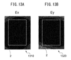
- FIGS. 13A and 13B each depict the intensity distribution of a direction component of the electric field in the x-y plane elevated 30 mm above the surface of the substrate 10 along the z axis. It is also assumed that the frequency of the radio wave having the design wavelength is 920 MHz.
- the distribution 1310 depicted in FIG. 13A represents the distribution of the x direction component of the electric field.
- the distribution 1320 depicted in FIG. 13B represents the distribution of the y direction component of the electric field. In the distributions 1310 and 1320 , darker areas indicate areas of stronger electric fields.
- the shelf antenna 2 also, it can be seen that at the position 30 mm above the upper surface of the substrate 10 , compared with the position 7 mm above the upper surface of the substrate 10 , the x and y direction components spread more uniformly while maintaining sufficient intensity.
- the shelf antenna 2 according to the second embodiment achieves the same effect as that achieved by the shelf antenna 1 of the first embodiment.
- one of the conductors 12 - 1 and 12 - 2 may be extended toward the feed point by one half of the design wavelength, and at the same time, the phases of the currents fed to the respective conductors 12 - 1 and 12 - 2 may be reversed with respect to each other.
- the phase of the current flowing through the conductor 12 - 1 and the phase of the current flowing through the conductor 12 - 2 are the same at every point taken along the longitudinal direction of the substrate 10 . Therefore, by arranging the resonators in the same manner as the resonators in the shelf antenna 2 of FIG. 11 , the strength of the electric field can be made uniform, as in the case of the shelf antenna 2 , regardless of the direction of the electric field.
- the feed points of the conductors 12 - 1 and 12 - 2 and the end points 12 - 1 b and 12 - 2 b at the other ends thereof may be short-circuited to the ground electrode 11 , for example, through vias formed in the substrate 10 .
- the end points 12 - 1 b and 12 - 2 b are fixed ends for the currents flowing through the respective microstrip lines.
- nodes are formed at every position spaced (1/4+n/2) ⁇ (n is an integer not smaller than 0, and ⁇ is the design wavelength) away from the end point 12 - 1 b along the conductor 12 - 1 .
- each resonator need only be shifted in position toward the feed point along the conductor 12 - 1 or 12 - 2 in such a manner that the distance from the end point 12 - 1 b or 12 - 2 b increases by (1/4) ⁇ .
- the feed point of one of the two parallelly arranged conductors and the end point at the other end thereof may be short-circuited to the ground electrode, for example, through vias formed in the substrate, and the end point of the other conductor, i.e., the end opposite to the feed point thereof, may be formed as an open end.
- FIG. 14 is a plan view of a shelf antenna according to this modified example.
- the shelf antenna 3 according to this modified example of the two line conductors 12 - 1 and 12 - 2 arranged parallel to each other on the surface of the substrate 10 , the end point 12 - 1 b of the conductor 12 - 1 is short-circuited through a via to the ground electrode (not depicted) formed on the lower surface of the substrate 10 .
- the conductor 12 - 1 is longer than the conductor 12 - 2 by one quarter of the design wavelength ⁇ .
- the end point 12 - 1 b of the conductor 12 - 1 is located one quarter of the design wavelength ⁇ farther away from the edge of the substrate 10 at which the respective feed points are located.
- the resonators 13 - 1 and 13 - 2 which resonate with the conductor 12 - 1 are each shifted one quarter of the design wavelength ⁇ farther away from the end point 12 - 1 b toward the feed point 12 - 1 a.
- the resonators 13 - 1 and 13 - 2 in the shelf antenna 3 are located at the same positions as the corresponding resonators in the shelf antenna 2 . Accordingly, the currents flowing through the respective resonators 13 - 1 to 13 - 4 are in phase. As a result, the electric fields generated from the respective resonators 13 - 1 to 13 - 4 are also in phase and can thus reinforce each other.
- the resonators 13 - 5 to 13 - 8 are arranged in the same manner as the resonators 13 - 5 to 13 - 8 in the second embodiment.
- the resonators 13 - 5 to 13 - 8 are arranged with their longitudinal direction substantially parallel to the longitudinal direction of the conductor 12 - 1 or 12 - 2 .
- the resonators 13 - 6 and 13 - 8 are in phase with each other.
- the phase of the circular polarization produced by the resonators 13 - 1 , 13 - 2 , 13 - 5 , and 13 - 6 becomes the same as that of the circular polarization produced by the resonators 13 - 3 , 13 - 4 , 13 - 7 , and 13 - 8 .
- each resonator is not limited to a loop shape, but a dipole antenna having a length equal to one half of the design wavelength, for example, may be employed as the resonator.
- the resonators (for example, the resonators 13 - 5 to 13 - 8 in FIG. 1 ) disposed with their longitudinal direction parallel to the two parallelly arranged conductors may be omitted.
- the electric field radiated from the shelf antenna is not circular polarization, but the uniformity of the electric field and the enhancement of the field strength can be achieved by the resonators that are arranged with their longitudinal direction perpendicular to the respective conductors.
- each resonator disposed between the two parallelly arranged conductors may be arranged so as to make an angle other than 90° with respect to the conductor to which it electromagnetically couples.
- the number of conductors forming the microstrip line is not limited to two, but may be three or more.
- FIG. 15 is a plan view of a shelf antenna according to this modified example.
- the shelf antenna 4 according to this modified example four line conductors 22 - 1 to 22 - 4 are arranged in parallel to each other on the substrate 10 .
- one end of the conductor 22 - 1 is a feed point 22 a.
- the other end of the conductor 22 - 1 and the end of the conductor 22 - 2 farther from the edge of the substrate 10 at which the feed point 22 a is located are connected by a line conductor 22 - 5 having a length equal to an integral multiple of the design wavelength.
- the other end of the conductor 22 - 2 and the end of the conductor 22 - 3 nearer to the edge of the substrate 10 at which the feed point 22 a is located are connected by a line conductor 22 - 6 having a length equal to an integral multiple of the design wavelength.
- the other end of the conductor 22 - 3 and the end of the conductor 22 - 4 farther from the edge of the substrate 10 at which the feed point 22 a is located are connected by a line conductor 22 - 7 having a length equal to an integral multiple of the design wavelength.
- the other end of the conductor 22 - 4 is an open end 22 b.
- each resonator is indicated by a line, but each resonator may be formed from a loop-shaped conductor whose loop length is approximately equal to the design wavelength.
- Each resonator is disposed so that one end of the resonator electromagnetically couples one of the conductors at a position whose distance from the open end 22 b, measured along the conductors 22 - 1 to 22 - 4 , is approximately equal to an integral multiple of one half of the design wavelength.
- the distance between any two adjacent resonators, measured along the longitudinal direction of the conductor, is approximately equal to the design wavelength.
- the resonators that electromagnetically couple respectively different conductors are arranged in alternating fashion so that each resonator that electromagnetically couples one conductor is spaced apart from its adjacent resonator that electromagnetically couples the other conductor by a distance approximately equal to one half of the design wavelength.
- the resonators may be arranged in a plane different from the plane in which the conductors forming the microstrip lines in combination with the ground electrode are arranged.
- FIG. 16A is a plan view of a shelf antenna according to this modified example
- FIG. 16B is a cross-sectional side view taken along line CC′ in FIG. 16A and viewed in the direction of the arrow.
- a substrate 30 formed from a dielectric material includes a first layer 30 - 1 and a second layer 30 - 2 in this order from the bottom.
- a ground electrode 31 is formed on the lower surface of the first layer 30 - 1 .
- a plurality of resonators 33 - 1 to 33 - 4 are arranged on the upper surface of the second layer 30 - 2 .
- the thickness of the first layer 30 - 1 and the thickness of the second layer 30 - 2 are chosen so that the characteristic impedance of the shelf antenna 5 becomes equal to a predetermined value.
- the thickness of the first layer 30 - 1 may be the same as, or different from, the thickness of the second layer 30 - 2 .
- the relative dielectric constant of the first layer 30 - 1 may be the same as, or different from, the relative dielectric constant of the second layer 30 - 2 .
- the conductors 32 - 1 and 32 - 2 each form a microstrip line in combination with the ground electrode 31 .
- the conductors 32 - 1 and 32 - 2 have the same length, are fed from the same side, and have open ends at the other ends.
- the other ends of the conductors 32 - 1 and 32 - 2 may be formed as fixed ends by being short-circuited to the ground electrode 31 .
- the resonators 33 - 1 and 33 - 2 are each disposed at a position spaced, for example, an integral multiple of the design wavelength ⁇ away from the open end of the conductor 32 - 1 along the longitudinal direction of the conductor 32 - 1 so as to resonate with the conductor 32 - 1 .
- the spacing between the resonators 33 - 1 and 33 - 2 along the longitudinal direction of the conductor 32 - 1 is approximately equal to the design wavelength ⁇ .
- the resonators 33 - 3 and 33 - 4 are each disposed at a position spaced, for example, a distance (integral multiple of ⁇ + ⁇ /2) away from the open end of the conductor 32 - 2 along the longitudinal direction of the conductor 32 - 2 so as to resonate with the conductor 32 - 2 .
- the spacing between the resonators 33 - 3 and 33 - 4 along the longitudinal direction of the conductor 32 - 1 is approximately equal to the design wavelength ⁇ .
- the resonators 33 - 1 to 33 - 4 are each formed as a dipole antenna having a length approximately equal to the design wavelength. Further, each of the resonators 33 - 1 to 33 - 4 is formed so that the portion thereof that is located between the conductors 32 - 1 and 32 - 2 extends in a direction perpendicular to the longitudinal direction of the conductor 32 - 1 . On the other hand, the portion of each of the resonators 33 - 1 to 33 - 4 that is not located between the conductors 32 - 1 and 32 - 2 may be formed in a serpentine fashion as depicted in FIG. 16A or may be formed in the shape of a straight line or curved line.
- the electric fields generated from the respective resonators are also in phase and can thus reinforce each other.
- the resonators used in this shelf antenna can be arranged with closer spacing than would be the case if the resonators were arranged along a single microstrip line, the electric field can be made uniform.
- the plurality of parallelly arranged conductors may be arranged along a direction other than the longitudinal direction of the substrate.
- the number of resonators need only be determined according to the size required of the antenna.
- the number of resonators that electromagnetically couple each of the two parallelly arranged conductors may be set to three or more.
- the number of resonators that electromagnetically couple one of the two parallelly arranged conductors may be set to two, and the number of resonators that electromagnetically couple the other conductor may be set to one.
Landscapes
- Physics & Mathematics (AREA)
- Electromagnetism (AREA)
- Waveguide Aerials (AREA)
- Variable-Direction Aerials And Aerial Arrays (AREA)
- Details Of Aerials (AREA)
Abstract
Description
Claims (10)
Applications Claiming Priority (2)
| Application Number | Priority Date | Filing Date | Title |
|---|---|---|---|
| JP2015131193A JP6548976B2 (en) | 2015-06-30 | 2015-06-30 | Flat antenna |
| JP2015-131193 | 2015-06-30 |
Publications (2)
| Publication Number | Publication Date |
|---|---|
| US20170005409A1 US20170005409A1 (en) | 2017-01-05 |
| US9819087B2 true US9819087B2 (en) | 2017-11-14 |
Family
ID=57684083
Family Applications (1)
| Application Number | Title | Priority Date | Filing Date |
|---|---|---|---|
| US15/170,695 Active US9819087B2 (en) | 2015-06-30 | 2016-06-01 | Planar antenna |
Country Status (2)
| Country | Link |
|---|---|
| US (1) | US9819087B2 (en) |
| JP (1) | JP6548976B2 (en) |
Families Citing this family (4)
| Publication number | Priority date | Publication date | Assignee | Title |
|---|---|---|---|---|
| JP6930591B2 (en) * | 2017-07-31 | 2021-09-01 | 株式会社村田製作所 | Antenna module and communication device |
| CN109950673B (en) * | 2019-04-02 | 2021-03-05 | 中国电子科技集团公司第三十八研究所 | A broadband stripline debugging structure with slow-wave characteristics and its design method |
| EP4146205A4 (en) | 2020-05-05 | 2024-05-29 | Nuvalent, Inc. | HETEROAROMATIC MACROCYCLIC ETHER-BASED CHEMOTHERAPY AGENTS |
| CN113036420B (en) * | 2021-05-13 | 2021-11-02 | 网络通信与安全紫金山实验室 | Antenna unit and antenna module |
Citations (1)
| Publication number | Priority date | Publication date | Assignee | Title |
|---|---|---|---|---|
| JP2014090291A (en) | 2012-10-30 | 2014-05-15 | Hitachi Chemical Co Ltd | Multilayer transmission line plate having electromagnetic coupling structure and antenna module |
Family Cites Families (2)
| Publication number | Priority date | Publication date | Assignee | Title |
|---|---|---|---|---|
| JPS57188104A (en) * | 1981-05-14 | 1982-11-19 | Kiyohiko Ito | Polarization switching type straight line polarized antenna |
| JP6232946B2 (en) * | 2013-11-07 | 2017-11-22 | 富士通株式会社 | Planar antenna |
-
2015
- 2015-06-30 JP JP2015131193A patent/JP6548976B2/en active Active
-
2016
- 2016-06-01 US US15/170,695 patent/US9819087B2/en active Active
Patent Citations (1)
| Publication number | Priority date | Publication date | Assignee | Title |
|---|---|---|---|---|
| JP2014090291A (en) | 2012-10-30 | 2014-05-15 | Hitachi Chemical Co Ltd | Multilayer transmission line plate having electromagnetic coupling structure and antenna module |
Also Published As
| Publication number | Publication date |
|---|---|
| JP6548976B2 (en) | 2019-07-24 |
| JP2017017475A (en) | 2017-01-19 |
| US20170005409A1 (en) | 2017-01-05 |
Similar Documents
| Publication | Publication Date | Title |
|---|---|---|
| US9831556B2 (en) | Planar antenna | |
| US8179329B2 (en) | Composite antenna | |
| JP4930359B2 (en) | Antenna device | |
| US20170077599A1 (en) | Multi-antenna and radio apparatus including thereof | |
| EP3127186B1 (en) | Dual-band printed omnidirectional antenna | |
| US20130300624A1 (en) | Broadband end-fire multi-layer antenna | |
| JP2006524940A (en) | Antenna device | |
| WO2005067549A2 (en) | Multi frequency magnetic dipole antenna structures and methods of reusing the volume of an antenna | |
| US9819087B2 (en) | Planar antenna | |
| US20140054383A1 (en) | Near field antenna | |
| US20200196439A1 (en) | Antenna device | |
| US10992047B2 (en) | Compact folded dipole antenna with multiple frequency bands | |
| US20150200461A1 (en) | Antenna apparatus | |
| JPWO2013145623A1 (en) | ANTENNA DEVICE AND PORTABLE RADIO DEVICE HAVING THE SAME | |
| Kabiri et al. | Gain-bandwidth enhancement of 60GHz single-layer Fabry-Perot cavity antennas using sparse-array | |
| CN116960623A (en) | An antenna and electronic device | |
| WO2018163695A1 (en) | Multiband antenna and wireless communication device | |
| CN111373603B (en) | Communication device | |
| JP2011217203A (en) | Planar loop antenna | |
| TWI401605B (en) | Circularly polarized microstrip antenna for rfid tag | |
| EP3059803A1 (en) | An antenna element, an interconnect, a method and an antenna array | |
| Necibi et al. | A New 30 GHz AMC/PRS RFID Reader Antenna with Circular Polarization | |
| JP2016058843A (en) | Planar antenna | |
| Alvina et al. | A triple band bow tie array antenna using both-sided MIC technology | |
| JP6059779B1 (en) | Dipole antenna and manufacturing method thereof |
Legal Events
| Date | Code | Title | Description |
|---|---|---|---|
| AS | Assignment |
Owner name: FUJITSU LIMITED, JAPAN Free format text: ASSIGNMENT OF ASSIGNORS INTEREST;ASSIGNORS:YAMAGAJO, TAKASHI;KAI, MANABU;SHIMIZU, MASAHIKO;AND OTHERS;SIGNING DATES FROM 20160421 TO 20160513;REEL/FRAME:038867/0812 Owner name: FUJITSU FRONTECH LIMITED, JAPAN Free format text: ASSIGNMENT OF ASSIGNORS INTEREST;ASSIGNORS:YAMAGAJO, TAKASHI;KAI, MANABU;SHIMIZU, MASAHIKO;AND OTHERS;SIGNING DATES FROM 20160421 TO 20160513;REEL/FRAME:038867/0812 |
|
| STCF | Information on status: patent grant |
Free format text: PATENTED CASE |
|
| MAFP | Maintenance fee payment |
Free format text: PAYMENT OF MAINTENANCE FEE, 4TH YEAR, LARGE ENTITY (ORIGINAL EVENT CODE: M1551); ENTITY STATUS OF PATENT OWNER: LARGE ENTITY Year of fee payment: 4 |
|
| AS | Assignment |
Owner name: FUJITSU FRONTECH LIMITED, JAPAN Free format text: ASSIGNMENT OF ASSIGNORS INTEREST;ASSIGNOR:FUJITSU LIMITED;REEL/FRAME:064550/0314 Effective date: 20230720 |
|
| MAFP | Maintenance fee payment |
Free format text: PAYMENT OF MAINTENANCE FEE, 8TH YEAR, LARGE ENTITY (ORIGINAL EVENT CODE: M1552); ENTITY STATUS OF PATENT OWNER: LARGE ENTITY Year of fee payment: 8 |