EP2866037A1 - Releaseable probe connection - Google Patents
Releaseable probe connection Download PDFInfo
- Publication number
- EP2866037A1 EP2866037A1 EP20140190306 EP14190306A EP2866037A1 EP 2866037 A1 EP2866037 A1 EP 2866037A1 EP 20140190306 EP20140190306 EP 20140190306 EP 14190306 A EP14190306 A EP 14190306A EP 2866037 A1 EP2866037 A1 EP 2866037A1
- Authority
- EP
- European Patent Office
- Prior art keywords
- probe
- interposer
- tab
- test
- connector
- Prior art date
- Legal status (The legal status is an assumption and is not a legal conclusion. Google has not performed a legal analysis and makes no representation as to the accuracy of the status listed.)
- Granted
Links
Images
Classifications
-
- H—ELECTRICITY
- H05—ELECTRIC TECHNIQUES NOT OTHERWISE PROVIDED FOR
- H05K—PRINTED CIRCUITS; CASINGS OR CONSTRUCTIONAL DETAILS OF ELECTRIC APPARATUS; MANUFACTURE OF ASSEMBLAGES OF ELECTRICAL COMPONENTS
- H05K1/00—Printed circuits
- H05K1/02—Details
-
- G—PHYSICS
- G01—MEASURING; TESTING
- G01R—MEASURING ELECTRIC VARIABLES; MEASURING MAGNETIC VARIABLES
- G01R1/00—Details of instruments or arrangements of the types included in groups G01R5/00 - G01R13/00 and G01R31/00
- G01R1/02—General constructional details
- G01R1/04—Housings; Supporting members; Arrangements of terminals
- G01R1/0408—Test fixtures or contact fields; Connectors or connecting adaptors; Test clips; Test sockets
- G01R1/0416—Connectors, terminals
-
- G—PHYSICS
- G01—MEASURING; TESTING
- G01R—MEASURING ELECTRIC VARIABLES; MEASURING MAGNETIC VARIABLES
- G01R31/00—Arrangements for testing electric properties; Arrangements for locating electric faults; Arrangements for electrical testing characterised by what is being tested not provided for elsewhere
- G01R31/28—Testing of electronic circuits, e.g. by signal tracer
- G01R31/2851—Testing of integrated circuits [IC]
- G01R31/2886—Features relating to contacting the IC under test, e.g. probe heads; chucks
-
- G—PHYSICS
- G01—MEASURING; TESTING
- G01R—MEASURING ELECTRIC VARIABLES; MEASURING MAGNETIC VARIABLES
- G01R31/00—Arrangements for testing electric properties; Arrangements for locating electric faults; Arrangements for electrical testing characterised by what is being tested not provided for elsewhere
- G01R31/28—Testing of electronic circuits, e.g. by signal tracer
- G01R31/2851—Testing of integrated circuits [IC]
- G01R31/2886—Features relating to contacting the IC under test, e.g. probe heads; chucks
- G01R31/2889—Interfaces, e.g. between probe and tester
Definitions
- the system includes a probe tab connected to a circuit, and a connector that can be releasably attached to the probe tab in order to measure signals on the circuit.
- Interposers are devices that are typically inserted between a memory integrated circuit (IC) chip and the printed circuit board that the memory IC chip normally mounts on.
- the interposers are small printed circuit boards or flexible circuits that sample the signals between the memory IC chip and the printed circuit board.
- a test and measurement instrument such as an oscilloscope, can be connected to the interposer through a probe to measure the signals.
- the test and measurement instrument is connected to the interposer through a browser probe or a solder down probe tab.
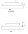
- An example of a set up for a solder down probe is shown in Figure 1 , which is not drawn to scale.
- An interposer 100 is mounted on a printed circuit board 102.
- the memory IC chip 104 is on top of the interposer 100.
- a solder point 106 is provided on the interposer to solder the probe tip of the test and measurement instrument.
- Solder down probes are difficult to use due to the small geometry and high bandwidths needed for modem memory systems. Browser probes are also difficult to use because the browser probes need to be held in place on the interposer and also may have a lower bandwidth than solder down probes. What is needed is an easily connectable probe to an interposer to quickly and accurately sample the signals between the memory IC chip and a printed circuit board.
- test and measurement probe connection system including an interposer, at least one probe tab connected to the interposer, and a connector that is releasably connectable to the at least one probe tab to measure signals from the interposer.
- Certain embodiments include a test and measurement probe connection system including a circuit, at least one probe tab connected to the interposer, and a connector that is releasably connectable to the at least one probe tab to measure signals from the interposer.
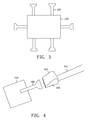
- FIG. 2 illustrates an interposer 200 located between a circuit 202 and a memory IC chip 204. Rather than a soldering point on the interposer to attach a solder down probe, a probe tab 206 is attached to the interposer 200. The probe tab 206 is part of the interposer 200. The probe tab 206 allows a test and measurement instrument to sample a signal from the memory IC chip 204 placed on top of the interposer 200. As will described in further detail below, a connector, which is attached to a test and measurement instrument, can easily be releasably connected to read signals from interposer 200.
- Figure 3 illustrates an example of an interposer 200 with six probe tabs 206.
- the probe tabs 206 are preferably manufactured as part of the interposer 200. That is, probe tabs 206 are integrally formed with the interposer 200.
- the probe tabs 206 may also be soldered onto the interposer 200 during manufacturing or by a user.
- Each probe tab 206 allows a different signal to be measured of the IC chip or circuit that is connected to the interposer 200.
- Figure 3 illustrates six probe tabs 206, the disclosed technology is not limited to six probe tabs 206.
- a single probe tab 206 could be used as shown Figure 2 or any number of probe tabs that can fit and are needed on an interposer.
- Each probe tab 206 brings out a desired signal from the circuit, as will be discussed in more detail below.
- the probe tabs 206 are used in a similar manner as the soldering points 106 are used in traditional interposers 100.
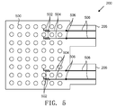
- Figure 4 illustrates the connection between a probe tab 406 and a connector 402.
- the probe tab 406 as shown in Figure 4 , is attached to a circuit 400 to bring out a desired signal from the circuit.
- Probe tab 406 works the same as probe tab 206 described above.
- the circuit 400 may be an interposer, as discussed above.
- Connector 402 can then be releasably attached to the probe tab 406 to measure the signal from the circuit 400. Then, if it is desired for another signal to be measured, the connector 402 can be removed from the current probe tab 406 and placed on another probe tab 406. This eliminates the need for a solder down probe and allows a user to easily measure a desired signal without requiring the skills of being able to solder the solder down probe to the interposer.
- Figure 4 shows a single probe tab 406 and a single connector 402
- the disclosed technology can have multiple probe tabs 406 on the circuit 400, similar to that shown in Figure 3 .
- multiple connectors 402 can be used as well, each connector 402 connected to a different probe tab.
- Connector 402 is attached to the end of a coaxial or flex cable assembly 404 which connects back to a test and measurement instrument (not shown). Multiple coaxial or flex cable assemblies 404 can be provided. Each of the coaxial or flex cable assembles 404 having a connector 402 at the end to measure signals from the probe tabs 406 are attached to a test and measurement signals and allows for multiple signals to be measured at once.
- Connector 402 is releasably connectable to a probe tab 406. This can be done a variety of ways.
- the connector 402 can have a slot 408 to insert the probe tab 406, as shown in Figure 4 .
- the top of the connector 402 can be opened and the probe tab 406 can be placed inside the connector 402. Then the top of connector 402 can be clamped down on the probe tab 406. In order to remove the probe tab 406, the top of the connector 402 merely needs to be opened again.
- the connector 402 being releasably attached allows a user to quickly and efficiently measure signals without requiring the skills to solder a solder down probe tab on to a small interposer or circuit.
- probe tabs 206 and 406 and connector 402 are built to withstand higher bandwidths and allow a user to be able to accurately sample or measure signals from circuits with higher bandwidths.
- Probe tabs 206 and 406 are preferably a flexible circuit attached to the interposer 200. Probe tab 206, however, can also be printed circuit boards attached to the interposer 200 or circuit 400. The probe tab 206 must be able to releasably connect with the connector 402. The probe tab 206 has electrical leads thereon to direct the signals sampled from the memory IC chip 204 through the interposer 200 to the end of the probe tab 206.
- the connector described in more detail below with respect to Figure 4 , can releasably attach to the probe tab 206 and read the signal that traveled through the electrical lead on the probe tab 206.
- Figure 5 shows an example of an interposer 200.
- the interposer 200 includes a variety of vias or solder pads 500, which are used to mount an IC chip, such as the memory IC chip 204 discussed above.
- the interposer 200 also includes probe tabs 206.
- the interposer 200 also includes internal resistors 502 shown in Figure 5 .
- the internal resistors 502 are connected to an internal metal trace 504 on the interposer 200. This internal metal trace 504 is connected to a via 506 and a surface metal trace 508.
- the signal from the memory IC chip 204 travels from the internal resistor 502, through internal metal trace 504 to the surface metal trace 508 through via 506.
- Connector 402 includes two conductors (not shown). The two conductors align with the surface metal trace 508 on the probe tabs 206. The signal on the surface metal trace 508 is then sent to the test and measurement instrument through the two conductors in the connector 402.
- an interposer in use with a memory IC chip has been discussed above, the disclosed technology is not limited to such an embodiment.
- An interposer with probe tabs can be used with any IC chip.
- the disclosed technology is not limited to use with an interposer. Rather, the technology can be used with any type of circuit in which it is desirable to measure a signal within the circuit.
- a probe tab can attached to the circuit and the connector can connect to the probe tab to measure the signal.
- the disclosed technology allows for signals to be measured within small spaces without having to solder down a probe tab or hold a browser probe tab.
- a user can quickly measure a variety of signals within a circuit by merely placing the connector on a probe tab, measuring the signal, and then disconnecting the connector and placing it on the next probe tab.
- the probe tabs 206 can take on any shape as long as they can connect to a connector 402.
- the shape of the probe tabs 206 and 406 does not matter.
- the shape can be as seen in Figures 3 and 4 , or the probe tabs 206 and 406 can take on a simpler shape of a rectangle as shown in Figure 5 .
Landscapes
- Physics & Mathematics (AREA)
- General Physics & Mathematics (AREA)
- Engineering & Computer Science (AREA)
- Microelectronics & Electronic Packaging (AREA)
- Measuring Leads Or Probes (AREA)
- Testing Of Individual Semiconductor Devices (AREA)
Abstract
Description
- This disclosure relates to a test and measurement probe connection system. The system includes a probe tab connected to a circuit, and a connector that can be releasably attached to the probe tab in order to measure signals on the circuit.
- Interposers are devices that are typically inserted between a memory integrated circuit (IC) chip and the printed circuit board that the memory IC chip normally mounts on. The interposers are small printed circuit boards or flexible circuits that sample the signals between the memory IC chip and the printed circuit board. A test and measurement instrument, such as an oscilloscope, can be connected to the interposer through a probe to measure the signals.
- Typically, the test and measurement instrument is connected to the interposer through a browser probe or a solder down probe tab. An example of a set up for a solder down probe is shown in
Figure 1 , which is not drawn to scale. Aninterposer 100 is mounted on a printedcircuit board 102. Thememory IC chip 104 is on top of theinterposer 100. Asolder point 106 is provided on the interposer to solder the probe tip of the test and measurement instrument. Solder down probes are difficult to use due to the small geometry and high bandwidths needed for modem memory systems. Browser probes are also difficult to use because the browser probes need to be held in place on the interposer and also may have a lower bandwidth than solder down probes. What is needed is an easily connectable probe to an interposer to quickly and accurately sample the signals between the memory IC chip and a printed circuit board. - Certain embodiments of the disclosed technology include a test and measurement probe connection system including an interposer, at least one probe tab connected to the interposer, and a connector that is releasably connectable to the at least one probe tab to measure signals from the interposer.
- Certain embodiments include a test and measurement probe connection system including a circuit, at least one probe tab connected to the interposer, and a connector that is releasably connectable to the at least one probe tab to measure signals from the interposer.
-
-
FIGURE 1 illustrates an example of a traditional interposer with a soldering point for a solder down probe tab. -
FIGURE 2 illustrates an example of an interposer with a probe tab of the disclosed technology. -
FIGURE 3 illustrates an interposer with multiple probe tabs attached. -
FIGURE 4 illustrates a probe tab connection system for connecting a connector to a probe tab. -
FIGURE 5 illustrates an interposer of the disclosed technology. - In the drawings, which are not to scale, like or corresponding elements of the disclosed systems and methods are denoted by the same reference numerals.
- The technology disclosed herein eliminates the need for browser probes and solder down probes to measure signals on various circuits.
Figure 2 illustrates aninterposer 200 located between acircuit 202 and amemory IC chip 204. Rather than a soldering point on the interposer to attach a solder down probe, aprobe tab 206 is attached to theinterposer 200. Theprobe tab 206 is part of theinterposer 200. Theprobe tab 206 allows a test and measurement instrument to sample a signal from thememory IC chip 204 placed on top of theinterposer 200. As will described in further detail below, a connector, which is attached to a test and measurement instrument, can easily be releasably connected to read signals frominterposer 200. -
Figure 3 illustrates an example of aninterposer 200 with sixprobe tabs 206. Theprobe tabs 206 are preferably manufactured as part of theinterposer 200. That is,probe tabs 206 are integrally formed with theinterposer 200. Theprobe tabs 206, however, may also be soldered onto theinterposer 200 during manufacturing or by a user. - Each
probe tab 206 allows a different signal to be measured of the IC chip or circuit that is connected to theinterposer 200. AlthoughFigure 3 illustrates sixprobe tabs 206, the disclosed technology is not limited to sixprobe tabs 206. Asingle probe tab 206 could be used as shownFigure 2 or any number of probe tabs that can fit and are needed on an interposer. Eachprobe tab 206 brings out a desired signal from the circuit, as will be discussed in more detail below. Theprobe tabs 206 are used in a similar manner as thesoldering points 106 are used intraditional interposers 100. -
Figure 4 illustrates the connection between aprobe tab 406 and aconnector 402. Theprobe tab 406, as shown inFigure 4 , is attached to acircuit 400 to bring out a desired signal from the circuit.Probe tab 406 works the same asprobe tab 206 described above. For example, thecircuit 400 may be an interposer, as discussed above.Connector 402 can then be releasably attached to theprobe tab 406 to measure the signal from thecircuit 400. Then, if it is desired for another signal to be measured, theconnector 402 can be removed from thecurrent probe tab 406 and placed on anotherprobe tab 406. This eliminates the need for a solder down probe and allows a user to easily measure a desired signal without requiring the skills of being able to solder the solder down probe to the interposer. - Although
Figure 4 shows asingle probe tab 406 and asingle connector 402, the disclosed technology can havemultiple probe tabs 406 on thecircuit 400, similar to that shown inFigure 3 . Further,multiple connectors 402 can be used as well, eachconnector 402 connected to a different probe tab. -
Connector 402 is attached to the end of a coaxial orflex cable assembly 404 which connects back to a test and measurement instrument (not shown). Multiple coaxial orflex cable assemblies 404 can be provided. Each of the coaxial or flex cable assembles 404 having aconnector 402 at the end to measure signals from theprobe tabs 406 are attached to a test and measurement signals and allows for multiple signals to be measured at once. -
Connector 402, as mentioned above, is releasably connectable to aprobe tab 406. This can be done a variety of ways. Theconnector 402 can have aslot 408 to insert theprobe tab 406, as shown inFigure 4 . In another embodiment, the top of theconnector 402 can be opened and theprobe tab 406 can be placed inside theconnector 402. Then the top ofconnector 402 can be clamped down on theprobe tab 406. In order to remove theprobe tab 406, the top of theconnector 402 merely needs to be opened again. Theconnector 402 being releasably attached allows a user to quickly and efficiently measure signals without requiring the skills to solder a solder down probe tab on to a small interposer or circuit. - Further, the
probe tabs connector 402 are built to withstand higher bandwidths and allow a user to be able to accurately sample or measure signals from circuits with higher bandwidths. -
Probe tabs interposer 200.Probe tab 206, however, can also be printed circuit boards attached to theinterposer 200 orcircuit 400. Theprobe tab 206 must be able to releasably connect with theconnector 402. Theprobe tab 206 has electrical leads thereon to direct the signals sampled from thememory IC chip 204 through theinterposer 200 to the end of theprobe tab 206. The connector, described in more detail below with respect toFigure 4 , can releasably attach to theprobe tab 206 and read the signal that traveled through the electrical lead on theprobe tab 206. -
Figure 5 shows an example of aninterposer 200. Theinterposer 200 includes a variety of vias orsolder pads 500, which are used to mount an IC chip, such as thememory IC chip 204 discussed above. Theinterposer 200 also includesprobe tabs 206. Theinterposer 200 also includesinternal resistors 502 shown inFigure 5 . Theinternal resistors 502 are connected to aninternal metal trace 504 on theinterposer 200. Thisinternal metal trace 504 is connected to a via 506 and asurface metal trace 508. The signal from thememory IC chip 204 travels from theinternal resistor 502, throughinternal metal trace 504 to thesurface metal trace 508 through via 506. -
Connector 402 includes two conductors (not shown). The two conductors align with thesurface metal trace 508 on theprobe tabs 206. The signal on thesurface metal trace 508 is then sent to the test and measurement instrument through the two conductors in theconnector 402. - Although an interposer in use with a memory IC chip has been discussed above, the disclosed technology is not limited to such an embodiment. An interposer with probe tabs can be used with any IC chip. Further, the disclosed technology is not limited to use with an interposer. Rather, the technology can be used with any type of circuit in which it is desirable to measure a signal within the circuit. A probe tab can attached to the circuit and the connector can connect to the probe tab to measure the signal. The disclosed technology allows for signals to be measured within small spaces without having to solder down a probe tab or hold a browser probe tab. A user can quickly measure a variety of signals within a circuit by merely placing the connector on a probe tab, measuring the signal, and then disconnecting the connector and placing it on the next probe tab.
- Further, the
probe tabs 206 can take on any shape as long as they can connect to aconnector 402. The shape of theprobe tabs Figures 3 and 4 , or theprobe tabs Figure 5 . - Having described and illustrated the principles of the disclosed technology in a preferred embodiment thereof, it should be apparent that the disclosed technology can be modified in arrangement and detail without departing from such principles. We claim all modifications and variations coming within the scope of the following claims.
Claims (12)
- A test and measurement probe connection system, comprising:an interposer;at least one probe tab connected to the interposer; anda connector that is releasably connectable to the at least one probe tab to measure signals from the interposer.
- The test and measurement probe connection system of claim 1, further comprising at least two probe tabs connected to the interposer.
- The test and measurement probe connection system of claim 2, wherein the connector can be removed from one probe tab and releasably attached to another probe tab to measure a different signal from the interposer.
- The test and measurement probe connection system of claim 1, wherein the at least one probe tab is a flexible circuit or a printed circuit board.
- The test and measurement probe connection system of claim 2, further comprising two connectors that are each releasably attachable to each of the at least two probe tabs to measure at least two signals from the interposer.
- The test and measurement probe connection system of claim 1, wherein the at least one probe tab is integrally formed with the interposer.
- A test and measurement probe connection system, comprising:a circuit;at least one probe tab connected to the circuit; anda connector that is releasably connectable to the at least one probe tab to measure signals from the circuit.
- The test and measurement probe connection system of claim 7, further comprising at least two probe tabs connected to the interposer.
- The test and measurement probe connection system of claim 8, wherein the connector can be removed from one probe tab and releasably attached to another probe tab to measure a different signal from the interposer.
- The test and measurement probe connection system of claim 7, wherein the at least one probe tab is a flexible circuit or a printed circuit board.
- The test and measurement probe connection system of claim 8, further comprising two connectors that are each releasably attachable to each of the at least two probe tabs to measure at least two signals from the interposer.
- The test and measurement probe connection system of claim 7, wherein the at least one probe tab is integrally formed with the interposer.
Applications Claiming Priority (1)
| Application Number | Priority Date | Filing Date | Title |
|---|---|---|---|
| US14/063,242 US9622336B2 (en) | 2013-10-25 | 2013-10-25 | Releasable probe connection |
Publications (2)
| Publication Number | Publication Date |
|---|---|
| EP2866037A1 true EP2866037A1 (en) | 2015-04-29 |
| EP2866037B1 EP2866037B1 (en) | 2025-04-16 |
Family
ID=51870821
Family Applications (1)
| Application Number | Title | Priority Date | Filing Date |
|---|---|---|---|
| EP14190306.2A Active EP2866037B1 (en) | 2013-10-25 | 2014-10-24 | Releaseable probe connection |
Country Status (4)
| Country | Link |
|---|---|
| US (1) | US9622336B2 (en) |
| EP (1) | EP2866037B1 (en) |
| JP (1) | JP2015083974A (en) |
| CN (1) | CN104569512A (en) |
Cited By (1)
| Publication number | Priority date | Publication date | Assignee | Title |
|---|---|---|---|---|
| US10886588B2 (en) | 2018-09-26 | 2021-01-05 | Keysight Technologies, Inc. | High dynamic range probe using pole-zero cancellation |
Families Citing this family (2)
| Publication number | Priority date | Publication date | Assignee | Title |
|---|---|---|---|---|
| US9142903B2 (en) * | 2013-11-22 | 2015-09-22 | Tektronix, Inc. | High performance multiport connector system using LIGA springs |
| US9568499B2 (en) * | 2013-11-22 | 2017-02-14 | Tektronix, Inc. | High performance LIGA spring interconnect system for probing application |
Citations (6)
| Publication number | Priority date | Publication date | Assignee | Title |
|---|---|---|---|---|
| US3953797A (en) * | 1972-11-20 | 1976-04-27 | Merlin Gerin | Electronic equipment assembly comprising plug-in modules and test bars |
| US5202622A (en) * | 1990-05-24 | 1993-04-13 | Tektronix, Inc. | Adapter and test fixture for an integrated circuit device package |
| US6060894A (en) * | 1997-03-03 | 2000-05-09 | Micron Technology, Inc. | Temporary package, method and system for testing semiconductor dice having backside electrodes |
| US6323670B1 (en) * | 1999-02-11 | 2001-11-27 | Taiwan Semiconductor Manufacturing Company | PCB adapter for IC chip failure analysis |
| US20040155328A1 (en) * | 2000-07-31 | 2004-08-12 | Kline Jerry D. | Wafer-interposer assembly |
| WO2008011106A2 (en) * | 2006-07-18 | 2008-01-24 | Octavian Scientific, Inc. | Methods and apparatus for flexible extension of electrical conductors beyond the edges of a substrate |
Family Cites Families (12)
| Publication number | Priority date | Publication date | Assignee | Title |
|---|---|---|---|---|
| JP3099547B2 (en) * | 1992-09-24 | 2000-10-16 | 日本電気株式会社 | Emulation probe |
| US6144559A (en) * | 1999-04-08 | 2000-11-07 | Agilent Technologies | Process for assembling an interposer to probe dense pad arrays |
| DE10002098A1 (en) * | 1999-04-08 | 2000-10-26 | Agilent Technologies Inc | System for testing dense connection area arrays has probe tip arrangement with connection area in array and probe tip resistance coupled to connection area and access transfer line |
| US6407568B1 (en) * | 2000-02-10 | 2002-06-18 | International Business Machines Corporation | Apparatus for probing ends of pins |
| US6914445B2 (en) * | 2002-09-06 | 2005-07-05 | Wei-Fang Fan | Modular socket for testing an integrated circuit |
| US20070057682A1 (en) * | 2005-09-15 | 2007-03-15 | Mctigue Michael T | Signal probe and probe assembly |
| CN201138360Y (en) * | 2007-12-13 | 2008-10-22 | 中芯国际集成电路制造(上海)有限公司 | Aging device |
| US7868625B2 (en) * | 2008-05-15 | 2011-01-11 | Tektronix, Inc. | Slot interposer probe |
| US9354122B2 (en) * | 2011-05-10 | 2016-05-31 | 3M Innovative Properties Company | Zero-heat-flux, deep tissue temperature measurement system |
| CN102495244A (en) * | 2011-11-29 | 2012-06-13 | 深圳市华星光电技术有限公司 | Testing connector, transmission wire, testing system and use method |
| US20140055159A1 (en) * | 2012-02-21 | 2014-02-27 | Nexus Technology | Interposer with Edge Probe Points |
| CN202956401U (en) * | 2012-11-08 | 2013-05-29 | 纬创资通股份有限公司 | Test board with gold finger structure that can be segmented and cut |
-
2013
- 2013-10-25 US US14/063,242 patent/US9622336B2/en active Active
-
2014
- 2014-10-23 JP JP2014216505A patent/JP2015083974A/en active Pending
- 2014-10-24 CN CN201410572924.9A patent/CN104569512A/en active Pending
- 2014-10-24 EP EP14190306.2A patent/EP2866037B1/en active Active
Patent Citations (6)
| Publication number | Priority date | Publication date | Assignee | Title |
|---|---|---|---|---|
| US3953797A (en) * | 1972-11-20 | 1976-04-27 | Merlin Gerin | Electronic equipment assembly comprising plug-in modules and test bars |
| US5202622A (en) * | 1990-05-24 | 1993-04-13 | Tektronix, Inc. | Adapter and test fixture for an integrated circuit device package |
| US6060894A (en) * | 1997-03-03 | 2000-05-09 | Micron Technology, Inc. | Temporary package, method and system for testing semiconductor dice having backside electrodes |
| US6323670B1 (en) * | 1999-02-11 | 2001-11-27 | Taiwan Semiconductor Manufacturing Company | PCB adapter for IC chip failure analysis |
| US20040155328A1 (en) * | 2000-07-31 | 2004-08-12 | Kline Jerry D. | Wafer-interposer assembly |
| WO2008011106A2 (en) * | 2006-07-18 | 2008-01-24 | Octavian Scientific, Inc. | Methods and apparatus for flexible extension of electrical conductors beyond the edges of a substrate |
Cited By (1)
| Publication number | Priority date | Publication date | Assignee | Title |
|---|---|---|---|---|
| US10886588B2 (en) | 2018-09-26 | 2021-01-05 | Keysight Technologies, Inc. | High dynamic range probe using pole-zero cancellation |
Also Published As
| Publication number | Publication date |
|---|---|
| JP2015083974A (en) | 2015-04-30 |
| CN104569512A (en) | 2015-04-29 |
| EP2866037B1 (en) | 2025-04-16 |
| US20150114685A1 (en) | 2015-04-30 |
| US9622336B2 (en) | 2017-04-11 |
Similar Documents
| Publication | Publication Date | Title |
|---|---|---|
| EP2166362A1 (en) | Probe assembly | |
| US6144559A (en) | Process for assembling an interposer to probe dense pad arrays | |
| US9261535B2 (en) | Active probe adaptor | |
| US6822466B1 (en) | Alignment/retention device for connector-less probe | |
| KR100500452B1 (en) | Ball Grid Array Package Test Apparatus and Method | |
| US8106672B2 (en) | Substrate inspection apparatus | |
| US10481176B2 (en) | High bandwidth differential lead with device connection | |
| US6783371B2 (en) | Solder-down printed circuit board connection structure | |
| US9622336B2 (en) | Releasable probe connection | |
| US7924036B2 (en) | Contactor assembly for integrated circuit testing | |
| US20150168447A1 (en) | Probe module | |
| CN113917194A (en) | Securing a probe to a device under test | |
| CN108205081A (en) | A kind of device measured for minute yardstick soldered ball return loss | |
| CN102539926A (en) | Four-line milliohmmeter and connectors thereof | |
| US7145352B2 (en) | Apparatus, method, and kit for probing a pattern of points on a printed circuit board | |
| US20100330830A1 (en) | Vertical probe intrface system | |
| CN208352559U (en) | A kind of test winding displacement | |
| US6638080B2 (en) | Integrated ball grid array-pin grid array-flex laminate test assembly | |
| CN102928634A (en) | Probe rod | |
| CN208607300U (en) | Batch testing device for microelectromechanical attitude measuring components | |
| US20110109340A1 (en) | Interface Adapter For Connecting With A Test Probe | |
| US20230045808A1 (en) | Systems, devices, and methods for testing integrated circuits in their native environments | |
| US20040221199A1 (en) | Systems and methods for probing processor signals | |
| US20220225495A1 (en) | Control circuit board | |
| CN117572213A (en) | A test structure and method applied to PCBA boards |
Legal Events
| Date | Code | Title | Description |
|---|---|---|---|
| PUAI | Public reference made under article 153(3) epc to a published international application that has entered the european phase |
Free format text: ORIGINAL CODE: 0009012 |
|
| 17P | Request for examination filed |
Effective date: 20141024 |
|
| AK | Designated contracting states |
Kind code of ref document: A1 Designated state(s): AL AT BE BG CH CY CZ DE DK EE ES FI FR GB GR HR HU IE IS IT LI LT LU LV MC MK MT NL NO PL PT RO RS SE SI SK SM TR |
|
| AX | Request for extension of the european patent |
Extension state: BA ME |
|
| R17P | Request for examination filed (corrected) |
Effective date: 20151029 |
|
| RBV | Designated contracting states (corrected) |
Designated state(s): AL AT BE BG CH CY CZ DE DK EE ES FI FR GB GR HR HU IE IS IT LI LT LU LV MC MK MT NL NO PL PT RO RS SE SI SK SM TR |
|
| STAA | Information on the status of an ep patent application or granted ep patent |
Free format text: STATUS: EXAMINATION IS IN PROGRESS |
|
| 17Q | First examination report despatched |
Effective date: 20180718 |
|
| GRAP | Despatch of communication of intention to grant a patent |
Free format text: ORIGINAL CODE: EPIDOSNIGR1 |
|
| STAA | Information on the status of an ep patent application or granted ep patent |
Free format text: STATUS: GRANT OF PATENT IS INTENDED |
|
| INTG | Intention to grant announced |
Effective date: 20241112 |
|
| RIN1 | Information on inventor provided before grant (corrected) |
Inventor name: ROCKWELL, MARTIN |
|
| GRAS | Grant fee paid |
Free format text: ORIGINAL CODE: EPIDOSNIGR3 |
|
| GRAA | (expected) grant |
Free format text: ORIGINAL CODE: 0009210 |
|
| STAA | Information on the status of an ep patent application or granted ep patent |
Free format text: STATUS: THE PATENT HAS BEEN GRANTED |
|
| P01 | Opt-out of the competence of the unified patent court (upc) registered |
Free format text: CASE NUMBER: APP_9469/2025 Effective date: 20250225 |
|
| AK | Designated contracting states |
Kind code of ref document: B1 Designated state(s): AL AT BE BG CH CY CZ DE DK EE ES FI FR GB GR HR HU IE IS IT LI LT LU LV MC MK MT NL NO PL PT RO RS SE SI SK SM TR |
|
| RAP3 | Party data changed (applicant data changed or rights of an application transferred) |
Owner name: TEKTRONIX, INC. |
|
| REG | Reference to a national code |
Ref country code: GB Ref legal event code: FG4D |
|
| RIN1 | Information on inventor provided before grant (corrected) |
Inventor name: ROCKWELL, MARTIN |
|
| REG | Reference to a national code |
Ref country code: CH Ref legal event code: EP Ref country code: DE Ref legal event code: R096 Ref document number: 602014091803 Country of ref document: DE |
|
| REG | Reference to a national code |
Ref country code: IE Ref legal event code: FG4D |
|
| REG | Reference to a national code |
Ref country code: NL Ref legal event code: MP Effective date: 20250416 |
|
| PG25 | Lapsed in a contracting state [announced via postgrant information from national office to epo] |
Ref country code: NL Free format text: LAPSE BECAUSE OF FAILURE TO SUBMIT A TRANSLATION OF THE DESCRIPTION OR TO PAY THE FEE WITHIN THE PRESCRIBED TIME-LIMIT Effective date: 20250416 |
|
| REG | Reference to a national code |
Ref country code: AT Ref legal event code: MK05 Ref document number: 1786044 Country of ref document: AT Kind code of ref document: T Effective date: 20250416 |
|
| PG25 | Lapsed in a contracting state [announced via postgrant information from national office to epo] |
Ref country code: PT Free format text: LAPSE BECAUSE OF FAILURE TO SUBMIT A TRANSLATION OF THE DESCRIPTION OR TO PAY THE FEE WITHIN THE PRESCRIBED TIME-LIMIT Effective date: 20250818 Ref country code: FI Free format text: LAPSE BECAUSE OF FAILURE TO SUBMIT A TRANSLATION OF THE DESCRIPTION OR TO PAY THE FEE WITHIN THE PRESCRIBED TIME-LIMIT Effective date: 20250416 Ref country code: ES Free format text: LAPSE BECAUSE OF FAILURE TO SUBMIT A TRANSLATION OF THE DESCRIPTION OR TO PAY THE FEE WITHIN THE PRESCRIBED TIME-LIMIT Effective date: 20250416 |
|
| REG | Reference to a national code |
Ref country code: LT Ref legal event code: MG9D |
|
| PG25 | Lapsed in a contracting state [announced via postgrant information from national office to epo] |
Ref country code: GR Free format text: LAPSE BECAUSE OF FAILURE TO SUBMIT A TRANSLATION OF THE DESCRIPTION OR TO PAY THE FEE WITHIN THE PRESCRIBED TIME-LIMIT Effective date: 20250717 Ref country code: NO Free format text: LAPSE BECAUSE OF FAILURE TO SUBMIT A TRANSLATION OF THE DESCRIPTION OR TO PAY THE FEE WITHIN THE PRESCRIBED TIME-LIMIT Effective date: 20250716 |
|
| PG25 | Lapsed in a contracting state [announced via postgrant information from national office to epo] |
Ref country code: PL Free format text: LAPSE BECAUSE OF FAILURE TO SUBMIT A TRANSLATION OF THE DESCRIPTION OR TO PAY THE FEE WITHIN THE PRESCRIBED TIME-LIMIT Effective date: 20250416 |
|
| PG25 | Lapsed in a contracting state [announced via postgrant information from national office to epo] |
Ref country code: BG Free format text: LAPSE BECAUSE OF FAILURE TO SUBMIT A TRANSLATION OF THE DESCRIPTION OR TO PAY THE FEE WITHIN THE PRESCRIBED TIME-LIMIT Effective date: 20250416 |
|
| PG25 | Lapsed in a contracting state [announced via postgrant information from national office to epo] |
Ref country code: HR Free format text: LAPSE BECAUSE OF FAILURE TO SUBMIT A TRANSLATION OF THE DESCRIPTION OR TO PAY THE FEE WITHIN THE PRESCRIBED TIME-LIMIT Effective date: 20250416 |
|
| PG25 | Lapsed in a contracting state [announced via postgrant information from national office to epo] |
Ref country code: AT Free format text: LAPSE BECAUSE OF FAILURE TO SUBMIT A TRANSLATION OF THE DESCRIPTION OR TO PAY THE FEE WITHIN THE PRESCRIBED TIME-LIMIT Effective date: 20250416 |
|
| PG25 | Lapsed in a contracting state [announced via postgrant information from national office to epo] |
Ref country code: RS Free format text: LAPSE BECAUSE OF FAILURE TO SUBMIT A TRANSLATION OF THE DESCRIPTION OR TO PAY THE FEE WITHIN THE PRESCRIBED TIME-LIMIT Effective date: 20250716 |
|
| PG25 | Lapsed in a contracting state [announced via postgrant information from national office to epo] |
Ref country code: IS Free format text: LAPSE BECAUSE OF FAILURE TO SUBMIT A TRANSLATION OF THE DESCRIPTION OR TO PAY THE FEE WITHIN THE PRESCRIBED TIME-LIMIT Effective date: 20250816 |
|
| PG25 | Lapsed in a contracting state [announced via postgrant information from national office to epo] |
Ref country code: LV Free format text: LAPSE BECAUSE OF FAILURE TO SUBMIT A TRANSLATION OF THE DESCRIPTION OR TO PAY THE FEE WITHIN THE PRESCRIBED TIME-LIMIT Effective date: 20250416 |
|
| PGFP | Annual fee paid to national office [announced via postgrant information from national office to epo] |
Ref country code: DE Payment date: 20251029 Year of fee payment: 12 |
|
| PG25 | Lapsed in a contracting state [announced via postgrant information from national office to epo] |
Ref country code: DK Free format text: LAPSE BECAUSE OF FAILURE TO SUBMIT A TRANSLATION OF THE DESCRIPTION OR TO PAY THE FEE WITHIN THE PRESCRIBED TIME-LIMIT Effective date: 20250416 Ref country code: SM Free format text: LAPSE BECAUSE OF FAILURE TO SUBMIT A TRANSLATION OF THE DESCRIPTION OR TO PAY THE FEE WITHIN THE PRESCRIBED TIME-LIMIT Effective date: 20250416 |
|
| REG | Reference to a national code |
Ref country code: DE Ref legal event code: R097 Ref document number: 602014091803 Country of ref document: DE |
|
| PG25 | Lapsed in a contracting state [announced via postgrant information from national office to epo] |
Ref country code: CZ Free format text: LAPSE BECAUSE OF FAILURE TO SUBMIT A TRANSLATION OF THE DESCRIPTION OR TO PAY THE FEE WITHIN THE PRESCRIBED TIME-LIMIT Effective date: 20250416 |
|
| PG25 | Lapsed in a contracting state [announced via postgrant information from national office to epo] |
Ref country code: EE Free format text: LAPSE BECAUSE OF FAILURE TO SUBMIT A TRANSLATION OF THE DESCRIPTION OR TO PAY THE FEE WITHIN THE PRESCRIBED TIME-LIMIT Effective date: 20250416 |
|
| PG25 | Lapsed in a contracting state [announced via postgrant information from national office to epo] |
Ref country code: SK Free format text: LAPSE BECAUSE OF FAILURE TO SUBMIT A TRANSLATION OF THE DESCRIPTION OR TO PAY THE FEE WITHIN THE PRESCRIBED TIME-LIMIT Effective date: 20250416 Ref country code: RO Free format text: LAPSE BECAUSE OF FAILURE TO SUBMIT A TRANSLATION OF THE DESCRIPTION OR TO PAY THE FEE WITHIN THE PRESCRIBED TIME-LIMIT Effective date: 20250416 |
|
| PG25 | Lapsed in a contracting state [announced via postgrant information from national office to epo] |
Ref country code: IT Free format text: LAPSE BECAUSE OF FAILURE TO SUBMIT A TRANSLATION OF THE DESCRIPTION OR TO PAY THE FEE WITHIN THE PRESCRIBED TIME-LIMIT Effective date: 20250416 |
|
| PLBE | No opposition filed within time limit |
Free format text: ORIGINAL CODE: 0009261 |
|
| STAA | Information on the status of an ep patent application or granted ep patent |
Free format text: STATUS: NO OPPOSITION FILED WITHIN TIME LIMIT |
|
| REG | Reference to a national code |
Ref country code: CH Ref legal event code: L10 Free format text: ST27 STATUS EVENT CODE: U-0-0-L10-L00 (AS PROVIDED BY THE NATIONAL OFFICE) Effective date: 20260225 |
|
| 26N | No opposition filed |
Effective date: 20260119 |
|
| REG | Reference to a national code |
Ref country code: CH Ref legal event code: H13 Free format text: ST27 STATUS EVENT CODE: U-0-0-H10-H13 (AS PROVIDED BY THE NATIONAL OFFICE) Effective date: 20260527 |
|
| PG25 | Lapsed in a contracting state [announced via postgrant information from national office to epo] |
Ref country code: LU Free format text: LAPSE BECAUSE OF NON-PAYMENT OF DUE FEES Effective date: 20251024 |
|
| REG | Reference to a national code |
Ref country code: BE Ref legal event code: MM Effective date: 20251031 |
|
| GBPC | Gb: european patent ceased through non-payment of renewal fee |
Effective date: 20251024 |
|
| PG25 | Lapsed in a contracting state [announced via postgrant information from national office to epo] |
Ref country code: LT Free format text: LAPSE BECAUSE OF FAILURE TO SUBMIT A TRANSLATION OF THE DESCRIPTION OR TO PAY THE FEE WITHIN THE PRESCRIBED TIME-LIMIT Effective date: 20250416 |
|
| PG25 | Lapsed in a contracting state [announced via postgrant information from national office to epo] |
Ref country code: MC Free format text: LAPSE BECAUSE OF FAILURE TO SUBMIT A TRANSLATION OF THE DESCRIPTION OR TO PAY THE FEE WITHIN THE PRESCRIBED TIME-LIMIT Effective date: 20250416 |
|
| PG25 | Lapsed in a contracting state [announced via postgrant information from national office to epo] |
Ref country code: GB Free format text: LAPSE BECAUSE OF NON-PAYMENT OF DUE FEES Effective date: 20251024 |
|
| PG25 | Lapsed in a contracting state [announced via postgrant information from national office to epo] |
Ref country code: BE Free format text: LAPSE BECAUSE OF NON-PAYMENT OF DUE FEES Effective date: 20251031 Ref country code: CH Free format text: LAPSE BECAUSE OF NON-PAYMENT OF DUE FEES Effective date: 20251031 |
|
| PG25 | Lapsed in a contracting state [announced via postgrant information from national office to epo] |
Ref country code: FR Free format text: LAPSE BECAUSE OF NON-PAYMENT OF DUE FEES Effective date: 20251031 |
|
| PG25 | Lapsed in a contracting state [announced via postgrant information from national office to epo] |
Ref country code: SE Free format text: LAPSE BECAUSE OF FAILURE TO SUBMIT A TRANSLATION OF THE DESCRIPTION OR TO PAY THE FEE WITHIN THE PRESCRIBED TIME-LIMIT Effective date: 20250416 |