EP2849546A1 - Circuit board and lighting device having the circiut board - Google Patents
Circuit board and lighting device having the circiut board Download PDFInfo
- Publication number
- EP2849546A1 EP2849546A1 EP14174746.9A EP14174746A EP2849546A1 EP 2849546 A1 EP2849546 A1 EP 2849546A1 EP 14174746 A EP14174746 A EP 14174746A EP 2849546 A1 EP2849546 A1 EP 2849546A1
- Authority
- EP
- European Patent Office
- Prior art keywords
- connector
- mounting portion
- circuit board
- region
- supporting substrate
- Prior art date
- Legal status (The legal status is an assumption and is not a legal conclusion. Google has not performed a legal analysis and makes no representation as to the accuracy of the status listed.)
- Granted
Links
Images


Classifications
-
- H—ELECTRICITY
- H05—ELECTRIC TECHNIQUES NOT OTHERWISE PROVIDED FOR
- H05K—PRINTED CIRCUITS; CASINGS OR CONSTRUCTIONAL DETAILS OF ELECTRIC APPARATUS; MANUFACTURE OF ASSEMBLAGES OF ELECTRICAL COMPONENTS
- H05K1/00—Printed circuits
- H05K1/02—Details
- H05K1/14—Structural association of two or more printed circuits
- H05K1/148—Arrangements of two or more hingeably connected rigid printed circuit boards, i.e. connected by flexible means
-
- G—PHYSICS
- G02—OPTICS
- G02B—OPTICAL ELEMENTS, SYSTEMS OR APPARATUS
- G02B6/00—Light guides; Structural details of arrangements comprising light guides and other optical elements, e.g. couplings
- G02B6/0001—Light guides; Structural details of arrangements comprising light guides and other optical elements, e.g. couplings specially adapted for lighting devices or systems
- G02B6/0011—Light guides; Structural details of arrangements comprising light guides and other optical elements, e.g. couplings specially adapted for lighting devices or systems the light guides being planar or of plate-like form
- G02B6/0066—Light guides; Structural details of arrangements comprising light guides and other optical elements, e.g. couplings specially adapted for lighting devices or systems the light guides being planar or of plate-like form characterised by the light source being coupled to the light guide
- G02B6/0068—Arrangements of plural sources, e.g. multi-colour light sources
-
- H—ELECTRICITY
- H05—ELECTRIC TECHNIQUES NOT OTHERWISE PROVIDED FOR
- H05K—PRINTED CIRCUITS; CASINGS OR CONSTRUCTIONAL DETAILS OF ELECTRIC APPARATUS; MANUFACTURE OF ASSEMBLAGES OF ELECTRICAL COMPONENTS
- H05K1/00—Printed circuits
- H05K1/02—Details
- H05K1/0277—Bendability or stretchability details
- H05K1/0278—Rigid circuit boards or rigid supports of circuit boards locally made bendable, e.g. by removal or replacement of material
-
- G—PHYSICS
- G02—OPTICS
- G02B—OPTICAL ELEMENTS, SYSTEMS OR APPARATUS
- G02B6/00—Light guides; Structural details of arrangements comprising light guides and other optical elements, e.g. couplings
- G02B6/0001—Light guides; Structural details of arrangements comprising light guides and other optical elements, e.g. couplings specially adapted for lighting devices or systems
- G02B6/0011—Light guides; Structural details of arrangements comprising light guides and other optical elements, e.g. couplings specially adapted for lighting devices or systems the light guides being planar or of plate-like form
- G02B6/0081—Mechanical or electrical aspects of the light guide and light source in the lighting device peculiar to the adaptation to planar light guides, e.g. concerning packaging
- G02B6/0083—Details of electrical connections of light sources to drivers, circuit boards, or the like
-
- H—ELECTRICITY
- H05—ELECTRIC TECHNIQUES NOT OTHERWISE PROVIDED FOR
- H05K—PRINTED CIRCUITS; CASINGS OR CONSTRUCTIONAL DETAILS OF ELECTRIC APPARATUS; MANUFACTURE OF ASSEMBLAGES OF ELECTRICAL COMPONENTS
- H05K2201/00—Indexing scheme relating to printed circuits covered by H05K1/00
- H05K2201/10—Details of components or other objects attached to or integrated in a printed circuit board
- H05K2201/10007—Types of components
- H05K2201/10106—Light emitting diode [LED]
-
- H—ELECTRICITY
- H05—ELECTRIC TECHNIQUES NOT OTHERWISE PROVIDED FOR
- H05K—PRINTED CIRCUITS; CASINGS OR CONSTRUCTIONAL DETAILS OF ELECTRIC APPARATUS; MANUFACTURE OF ASSEMBLAGES OF ELECTRICAL COMPONENTS
- H05K2201/00—Indexing scheme relating to printed circuits covered by H05K1/00
- H05K2201/10—Details of components or other objects attached to or integrated in a printed circuit board
- H05K2201/10007—Types of components
- H05K2201/10189—Non-printed connector
-
- H—ELECTRICITY
- H05—ELECTRIC TECHNIQUES NOT OTHERWISE PROVIDED FOR
- H05K—PRINTED CIRCUITS; CASINGS OR CONSTRUCTIONAL DETAILS OF ELECTRIC APPARATUS; MANUFACTURE OF ASSEMBLAGES OF ELECTRICAL COMPONENTS
- H05K2203/00—Indexing scheme relating to apparatus or processes for manufacturing printed circuits covered by H05K3/00
- H05K2203/30—Details of processes not otherwise provided for in H05K2203/01 - H05K2203/17
- H05K2203/302—Bending a rigid substrate; Breaking rigid substrates by bending
-
- H—ELECTRICITY
- H05—ELECTRIC TECHNIQUES NOT OTHERWISE PROVIDED FOR
- H05K—PRINTED CIRCUITS; CASINGS OR CONSTRUCTIONAL DETAILS OF ELECTRIC APPARATUS; MANUFACTURE OF ASSEMBLAGES OF ELECTRICAL COMPONENTS
- H05K3/00—Apparatus or processes for manufacturing printed circuits
- H05K3/36—Assembling printed circuits with other printed circuits
- H05K3/366—Assembling printed circuits with other printed circuits substantially perpendicularly to each other
Definitions
- Embodiments of the present invention relate to a circuit board and a lighting device having the circuit board.
- a liquid crystal display has no self-luminous which can make its own light, a separate lighting device is always needed for all the liquid crystal display devices.
- a lighting device serves as a light source of the liquid crystal display device, and a backlight unit (BLU) refers to a complex composed of a light source itself for irradiating light to a rear surface of a liquid module, a power circuit for driving the light source, and all components for enabling uniform flat light to be formed.
- BLU backlight unit
- the liquid crystal display device becomes gradually thin, and accordingly, a reduction in a bezel width of the liquid crystal display device has been needed.
- the structure of a circuit board on which light emitting devices are mounted, or the structure of a lighting device including a light guide plate for guiding light generated from the light emitting devices has been changed.
- An aspect of embodiments of the present invention may provide a circuit board which is configured such that a supporting substrate to which a connector is mounted is formed lower than a supporting substrate to which a connector is not mounted, thereby reducing a space occupied by the connector.
- Another aspect of embodiments of the present invention may provide a circuit board which is configured such that a supporting substrate to which a connector is mounted is formed lower than a supporting substrate to which a connector is not mounted so that light emitting elements can be prevented from being covered due to the connector, thereby enabling light efficiency to be improved.
- a further aspect of embodiments of the present invention may provide a circuit board which is configured such that a supporting substrate to which a connector is mounted and a supporting substrate to which a connector is not mounted are separated and spaced apart from each other, and a connecting portion is formed between the two supporting substrates so that a step difference between the two supporting substrates can be adjusted by the connecting portion.
- Yet another aspect of embodiments of the present invention may provide a circuit board which is configured such that a connecting portion for connecting a supporting substrate to which a connector is mounted and a supporting substrate to which a connector is not mounted is made of a flexible material so that a step difference between the two supporting substrates can be adjusted thanks to flexibility of the connection portion.
- Still another aspect of embodiments of the present invention may provide a circuit board which is configured such that a connecting portion is formed in a second region of a supporting substrate by which string wirings for transmitting electrical signals to light emitting elements pass, or the connecting portion is formed in the second region of the supporting substrate which does not overlap with bending holes so that the connecting portion can be formed in various shapes.
- Still further aspect of embodiments of the present invention may provide a circuit board which is configured such that a part of a first region of a supporting substrate corresponding to a connecting portion passes through a supporting substrate, or the first region connected to a second region to which a connector is mounted extends to the extent of a height of the connector so that the supporting substrate can be formed in various shapes.
- Still further aspect of embodiments of the present invention may provide a lighting device capable of reducing a bezel width of a display device, when a circuit board is applied to the display device, the circuit board being configured such that a supporting substrate to which a connector is mounted is formed lower than a supporting substrate to which a connector is not mounted so that a space occupied by the connector can be reduced.
- a circuit board may include a supporting substrate including a first region to which a light emitting element is mounted, and a second region extending to be bent from the first region, wherein the second region may include: a connector mounting portion to which a connector for supplying an electric current to the light emitting elements is mounted; and a non-mounting portion of a connector separated and spaced apart from the connector mounting portion, wherein the connector mounting portion may be formed lower than the non-mounting portion of the connector.
- the circuit board may further include a connecting portion disposed in a portion in which a part of the second region of the supporting substrate is removed, and configured to connect the connector mounting portion and the non-mounting portion of the connector.
- a circuit board may include: a supporting substrate including a first region and a second region extending to be bent from the first region; an insulating substrate on the supporting substrate; light emitting elements mounted to the first region; a connector mounting portion to which a connector for supplying an electric current to the light emitting elements is mounted, and which is placed in one part of the second region; a non-mounting portion of a connector separated and spaced apart from the connector mounting portion and placed in another part of the second region; and a connecting portion disposed in which the supporting substrate of the second region is removed, and which connects the connector mounting portion and the non-mounting portion of the connector using the insulating substrate.
- the connector mounting portion may be disposed lower than the non-mounting portion of the connector to the extent of a height of the connector.
- the connector mounting portion may be disposed lower than the non-mounting portion of the connector to the extent of a height of the light emitting elements.
- the connecting portion may be made of at least one of PET (polyethylene terephthalate), PC (polycarbonate), PES (polyether sulfone), PI (polyimide) and PMMA (PolyMethly MethaAcrylate).
- PET polyethylene terephthalate
- PC polycarbonate
- PES polyether sulfone
- PI polyimide
- PMMA PolyMethly MethaAcrylate
- the connecting portion may include string wirings for transmitting electrical signals to the light emitting elements.
- the circuit board may further comprising bending holes formed in a bending portion between the first region and the second region, wherein the connecting portion may be disposed in the second region except for the bending holes
- a part of the first region corresponding to the connecting portion may pass through the supporting substrate.
- the supporting substrate may be configured such that the first region connected to the connector mounting portion extends to the extent of the height of the connector.
- a lighting device may include a circuit board and a light guide plate disposed to be spaced apart from the circuit board.
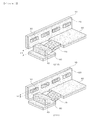
- FIG. 1 is a view illustrating a circuit board according to one embodiment of the present invention.
- a circuit board 110 includes: a supporting substrate 10 including a first region A to which light emitting elements 30 are mounted, and a second region B extending to be bent from the first region A; a connector mounting portion 50 of the second region B to which a connector for supplying an electric current to the light emitting elements 30 is mounted; and a non-mounting portion of a connector 60 separated and spaced apart from the connector mounting portion 50 in the second region B.
- the connector mounting portion 50 may be formed lower than the non-mounting portion of the connector 60.
- the circuit board 110 may further include: an insulating substrate 20 on the supporting substrate 10; and a connecting portion 70 disposed in a part passing through the second region B of the supporting substrate 10 and configured to connect the connector mounting portion 50 and the non-mounting portion of the connector 60.
- a circuit board of reference numeral 120 shows a view of the circuit board as viewed from a front surface when the connector 40 is mounted.
- the connecting portion 70 connects the connector mounting portion 50 and the non-mounting portion of the connector 60 which are separated from each other, and the circuit board 120 may show a state in which the supporting substrate 10 is removed, and only the insulating substrate 20 remains.
- the connecting portion 70 may be made of a flexible material having flexibility.
- the connecting portion 70 may be made of at least one of PET (polyethylene terephthalate), PC (polycarbonate), PES (polyether sulfone), PI (polyimide) and PMMA (PolyMethly MethaAcrylate). That is, the connecting portion 70 may be the insulating substrate 20, or may be made of the same material as that of the insulating substrate 20 or a flexible material different from that of the insulating substrate 20.
- FIG. 2 is a view illustrating an arrangement relation between the connector mounting portion and the non-mounting portion of the connector.
- the connector mounting portion 50 may be disposed lower than the non-mounting portion of the connector 60 to the extent of a height h1 of the connector 40 (210).
- the fact that the connector mounting portion 50 is disposed lower than the non-mounting portion of the connector 60 is intended not to cover the light emitting elements 30, and in consideration of the fact that the connector 40 is mounted to the connector mounting portion 50, the connector mounting portion 50 may be disposed lower than the non-mounting portion of the connector 60 to the extent of the height h1 of the connector 40.
- the connector mounting portion 50 may be disposed lower than the non-mounting portion of the connector 60 to the extent of a height h2 of the light emitting elements 30 (220). In order for the light emitting elements 30 not to be covered by the connector 40 mounted to the connector mounting portion 50, the connector mounting portion 50 may be disposed lower than the non-mounting portion of the connector 60 to the extent of the height h2 of the light emitting elements 30.
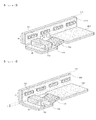
- FIGS. 3 and 4 are views illustrating one example of the connecting portion according to one embodiment of the present invention.
- the connecting portion 70 may include string wirings 70a for transmitting electrical signals to the light emitting elements 30.
- the connecting portion 70 may be formed only in the second region B by which the string wirings 70a passes.
- the circuit board may include bending holes 80 formed in a bending portion between the first region A and the second region B.
- the bending holes 80 are formed to enable the circuit board to be easily bent.
- the connecting portion 70 may be disposed in the second region B except for the bending holes 80. That is, the connecting portion 70 may be disposed in the second region B which does not overlap with the bending holes 80.
- FIGS. 5 and 6 are views illustrating one example of the supporting substrate according to one embodiment of the present invention.
- the supporting substrate 10 may be made of at least one of Al, Au, Ag, Cr, an organic compound, an inorganic compound, a magnetic material and a conductive material. That is, since the supporting substrate 10 may be made of a stronger material than that of the insulating substrate 20, the part (a) of the supporting substrate 10 of the first region A corresponding to a position in which the connecting portion 70 is formed may be removed so that the connecting portion 70 can enable a step difference between the connector mounting portion 50 and the non-mounting portion of the connector 60 to be easily overcome.
- a part d of the first region A connected to the connector mounting portion 50 may extend.
- the supporting substrate 10 may enable the first region A connected to the connector mounting portion 50 to extend to the extent of a height h1 of the connector 40. Accordingly, as the supporting substrate 10 of the first region A in which the connector mounting portion is formed extends to the extent of the height h1 of the connector 40, the connector mounting portion 50 and the non-mounting portion of the connector 60 may be more stably connected to each other.
- the circuit board according to one embodiment of the present invention may have pad wirings (not drawn) connected to the light emitting elements 30 mounted on the insulating substrate 20.
- the circuit board according to another embodiment of the present invention may be configured such that the insulating substrate 20 is formed on one surface of the first region A of the supporting substrate 10 and another surface opposite to the one surface, pad wirings connected to the light emitting elements 30 mounted on one surface of the insulating substrate 20 are formed, and string wirings for transmitting electrical signals to the light emitting elements are formed on another surface of the insulating substrate 20. Also, the string wirings may be formed at a side in which the one surface and the other surface of the insulating substrate 20 meet, and thus the string wirings and the pad wirings may be connected.
- the circuit board according to still another embodiment of the present invention may be configured such that the string wirings are formed in the bending holes 80 so that the string wirings and the pad wirings can be connected.
- the circuit board according to still another embodiment of the present invention may be configured such that the string wirings for transmitting electrical signals to the light emitting elements 30 are formed on another surface of the second region B of the insulating substrate 20.
- the circuit board according to still another embodiment of the present invention may be configured such that edge patterns are formed on at least one side of the supporting substrate 10.
- the lighting device may reduce a bezel width of a display device, when a circuit board is applied to the display device, by providing the circuit board configured such that a supporting substrate to which a connector is mounted is formed lower than a supporting substrate to which a connector is not mounted so that a space occupied by the connector can be reduced.
- the supporting substrate to which the connector is mounted is formed lower than the supporting substrate to which a connector is not mounted so that a space occupied by the connector can be reduced.
- the supporting substrate to which the connector is mounted is formed lower than the supporting substrate to which the connector is not mounted so that the light emitting elements can be prevented from being covered due to the connector, thereby enabling light efficiency to be improved.
- the supporting substrate to which the connector is mounted and the supporting substrate to which the connector is not mounted are separated and spaced apart from each other, and the connecting portion is formed between the two supporting substrates so that a step difference between the two supporting substrates can be adjusted by the connecting portion.
- the connecting portion for connecting the supporting substrate to which the connector is mounted and the supporting substrate to which the connector is not mounted is made of a flexible material so that a step difference between the two supporting substrates can be adjusted thanks to flexibility of the connection portion.
- the connecting portion is formed in the second region of the supporting substrate by which the string wirings for transmitting electrical signals to light emitting elements pass, or the connecting portion is formed in the second region of the supporting substrate which does not overlap with the bending holes so that the connecting portion can be formed in various shapes.
- the lighting device capable of reducing the bezel width of the display device, when a circuit board is applied to the display device, the circuit board being configured such that the supporting substrate to which the connector is mounted is formed lower than the supporting substrate to which the connector is not mounted so that the space occupied by the connector can be reduced.
Landscapes
- Engineering & Computer Science (AREA)
- Microelectronics & Electronic Packaging (AREA)
- Physics & Mathematics (AREA)
- General Physics & Mathematics (AREA)
- Optics & Photonics (AREA)
- Manufacturing & Machinery (AREA)
- Planar Illumination Modules (AREA)
- Fastening Of Light Sources Or Lamp Holders (AREA)
- Combinations Of Printed Boards (AREA)
- Coupling Device And Connection With Printed Circuit (AREA)
- Non-Portable Lighting Devices Or Systems Thereof (AREA)
- Led Device Packages (AREA)
- General Engineering & Computer Science (AREA)
- Structure Of Printed Boards (AREA)
Abstract
Description
- Embodiments of the present invention relate to a circuit board and a lighting device having the circuit board.
- A liquid crystal display (LCD) has no self-luminous which can make its own light, a separate lighting device is always needed for all the liquid crystal display devices. Such a lighting device serves as a light source of the liquid crystal display device, and a backlight unit (BLU) refers to a complex composed of a light source itself for irradiating light to a rear surface of a liquid module, a power circuit for driving the light source, and all components for enabling uniform flat light to be formed.
- The liquid crystal display device becomes gradually thin, and accordingly, a reduction in a bezel width of the liquid crystal display device has been needed. As one example, in order to reduce the bezel width, the structure of a circuit board on which light emitting devices are mounted, or the structure of a lighting device including a light guide plate for guiding light generated from the light emitting devices has been changed.
- However, even though the structure of the circuit board becomes thin, a shape of the connector for supplying an electric current to the light emitting elements has not been changed, and thus it is problematic in that it is difficult to reduce the bezel width due to the connector.
- Accordingly, ways to mount the connector to the circuit board have been practically needed.
- An aspect of embodiments of the present invention may provide a circuit board which is configured such that a supporting substrate to which a connector is mounted is formed lower than a supporting substrate to which a connector is not mounted, thereby reducing a space occupied by the connector.
- Another aspect of embodiments of the present invention may provide a circuit board which is configured such that a supporting substrate to which a connector is mounted is formed lower than a supporting substrate to which a connector is not mounted so that light emitting elements can be prevented from being covered due to the connector, thereby enabling light efficiency to be improved.
- A further aspect of embodiments of the present invention may provide a circuit board which is configured such that a supporting substrate to which a connector is mounted and a supporting substrate to which a connector is not mounted are separated and spaced apart from each other, and a connecting portion is formed between the two supporting substrates so that a step difference between the two supporting substrates can be adjusted by the connecting portion.
- Yet another aspect of embodiments of the present invention may provide a circuit board which is configured such that a connecting portion for connecting a supporting substrate to which a connector is mounted and a supporting substrate to which a connector is not mounted is made of a flexible material so that a step difference between the two supporting substrates can be adjusted thanks to flexibility of the connection portion.
- Still another aspect of embodiments of the present invention may provide a circuit board which is configured such that a connecting portion is formed in a second region of a supporting substrate by which string wirings for transmitting electrical signals to light emitting elements pass, or the connecting portion is formed in the second region of the supporting substrate which does not overlap with bending holes so that the connecting portion can be formed in various shapes.
- Still further aspect of embodiments of the present invention may provide a circuit board which is configured such that a part of a first region of a supporting substrate corresponding to a connecting portion passes through a supporting substrate, or the first region connected to a second region to which a connector is mounted extends to the extent of a height of the connector so that the supporting substrate can be formed in various shapes.
- Still further aspect of embodiments of the present invention may provide a lighting device capable of reducing a bezel width of a display device, when a circuit board is applied to the display device, the circuit board being configured such that a supporting substrate to which a connector is mounted is formed lower than a supporting substrate to which a connector is not mounted so that a space occupied by the connector can be reduced.
- According to an aspect of the embodiments of the present invention, a circuit board may include a supporting substrate including a first region to which a light emitting element is mounted, and a second region extending to be bent from the first region, wherein the second region may include: a connector mounting portion to which a connector for supplying an electric current to the light emitting elements is mounted; and a non-mounting portion of a connector separated and spaced apart from the connector mounting portion, wherein the connector mounting portion may be formed lower than the non-mounting portion of the connector.
- The circuit board may further include a connecting portion disposed in a portion in which a part of the second region of the supporting substrate is removed, and configured to connect the connector mounting portion and the non-mounting portion of the connector.
- According to another aspect of the embodiments of the present invention, a circuit board may include: a supporting substrate including a first region and a second region extending to be bent from the first region; an insulating substrate on the supporting substrate; light emitting elements mounted to the first region; a connector mounting portion to which a connector for supplying an electric current to the light emitting elements is mounted, and which is placed in one part of the second region; a non-mounting portion of a connector separated and spaced apart from the connector mounting portion and placed in another part of the second region; and a connecting portion disposed in which the supporting substrate of the second region is removed, and which connects the connector mounting portion and the non-mounting portion of the connector using the insulating substrate.
- The connector mounting portion may be disposed lower than the non-mounting portion of the connector to the extent of a height of the connector.
- The connector mounting portion may be disposed lower than the non-mounting portion of the connector to the extent of a height of the light emitting elements.
- The connecting portion may be made of at least one of PET (polyethylene terephthalate), PC (polycarbonate), PES (polyether sulfone), PI (polyimide) and PMMA (PolyMethly MethaAcrylate).
- The connecting portion may include string wirings for transmitting electrical signals to the light emitting elements.
- The circuit board may further comprising bending holes formed in a bending portion between the first region and the second region, wherein the connecting portion may be disposed in the second region except for the bending holes
- A part of the first region corresponding to the connecting portion may pass through the supporting substrate.
- The supporting substrate may be configured such that the first region connected to the connector mounting portion extends to the extent of the height of the connector.
- According to a further aspect of the embodiments of the present invention, a lighting device may include a circuit board and a light guide plate disposed to be spaced apart from the circuit board.
- The accompanying drawings are included to provide a further understanding of the present invention, and are incorporated in and constitute a part of this specification. The drawings illustrate exemplary embodiments of the present invention and, together with the description, serve to explain principles of the present invention. In the drawings:
-
FIG. 1 is a view illustrating a circuit board according to one embodiment of the present invention; -
FIG. 2 is a view illustrating an arrangement relation between a connector mounting portion and a non-mounting portion of a connector; -
FIGS. 3 and 4 are views illustrating one example of a connecting portion according to one embodiment of the present invention; and -
FIGS. 5 and 6 are views illustrating one example of a supporting substrate according to one embodiment of the present invention. - Hereinafter, the configurations and operations according to embodiments of the present invention will be described in detail with reference to the accompanying drawings. The present invention may, however, be embodied in different forms and should not be construed as limited to the embodiments set forth herein. In the explanation with reference to the accompanying drawings, regardless of reference numerals of the drawings, like numbers refer to like elements through the specification, and repeated explanation thereon is omitted. Terms such as a first term and a second term may be used for explaining various constitutive elements, but the constitutive elements should not be limited to these terms. These terms is used only for the purpose for distinguishing a constitutive element from other constitutive element.
-
FIG. 1 is a view illustrating a circuit board according to one embodiment of the present invention. - Referring to
FIG. 1 , acircuit board 110 includes: a supportingsubstrate 10 including a first region A to whichlight emitting elements 30 are mounted, and a second region B extending to be bent from the first region A; aconnector mounting portion 50 of the second region B to which a connector for supplying an electric current to thelight emitting elements 30 is mounted; and a non-mounting portion of aconnector 60 separated and spaced apart from theconnector mounting portion 50 in the second region B. In particular, theconnector mounting portion 50 may be formed lower than the non-mounting portion of theconnector 60. Here, thecircuit board 110 may further include: aninsulating substrate 20 on the supportingsubstrate 10; and a connectingportion 70 disposed in a part passing through the second region B of the supportingsubstrate 10 and configured to connect theconnector mounting portion 50 and the non-mounting portion of theconnector 60. - A circuit board of
reference numeral 120 shows a view of the circuit board as viewed from a front surface when theconnector 40 is mounted. The connectingportion 70 connects theconnector mounting portion 50 and the non-mounting portion of theconnector 60 which are separated from each other, and thecircuit board 120 may show a state in which the supportingsubstrate 10 is removed, and only theinsulating substrate 20 remains. - In one embodiment, the connecting
portion 70 may be made of a flexible material having flexibility. For example, the connectingportion 70 may be made of at least one of PET (polyethylene terephthalate), PC (polycarbonate), PES (polyether sulfone), PI (polyimide) and PMMA (PolyMethly MethaAcrylate). That is, the connectingportion 70 may be theinsulating substrate 20, or may be made of the same material as that of theinsulating substrate 20 or a flexible material different from that of theinsulating substrate 20. -
FIG. 2 is a view illustrating an arrangement relation between the connector mounting portion and the non-mounting portion of the connector. - Referring to
FIG. 2 , theconnector mounting portion 50 may be disposed lower than the non-mounting portion of theconnector 60 to the extent of a height h1 of the connector 40 (210). The fact that theconnector mounting portion 50 is disposed lower than the non-mounting portion of theconnector 60 is intended not to cover thelight emitting elements 30, and in consideration of the fact that theconnector 40 is mounted to theconnector mounting portion 50, theconnector mounting portion 50 may be disposed lower than the non-mounting portion of theconnector 60 to the extent of the height h1 of theconnector 40. - Also, the
connector mounting portion 50 may be disposed lower than the non-mounting portion of theconnector 60 to the extent of a height h2 of the light emitting elements 30 (220). In order for thelight emitting elements 30 not to be covered by theconnector 40 mounted to theconnector mounting portion 50, theconnector mounting portion 50 may be disposed lower than the non-mounting portion of theconnector 60 to the extent of the height h2 of thelight emitting elements 30. -
FIGS. 3 and 4 are views illustrating one example of the connecting portion according to one embodiment of the present invention. - Referring to
FIG. 3 , the connectingportion 70 may includestring wirings 70a for transmitting electrical signals to thelight emitting elements 30. For example, the connectingportion 70 may be formed only in the second region B by which thestring wirings 70a passes. - Referring to
FIG. 4 , the circuit board may include bendingholes 80 formed in a bending portion between the first region A and the second region B. Thebending holes 80 are formed to enable the circuit board to be easily bent. At this time, the connectingportion 70 may be disposed in the second region B except for thebending holes 80. That is, the connectingportion 70 may be disposed in the second region B which does not overlap with thebending holes 80. -
FIGS. 5 and 6 are views illustrating one example of the supporting substrate according to one embodiment of the present invention. - Referring to
FIG. 5 , in the supportingsubstrate 10, a part (a) of the first region A corresponding to the connectingportion 70 may be removed. For example, the supportingsubstrate 10 may be made of at least one of Al, Au, Ag, Cr, an organic compound, an inorganic compound, a magnetic material and a conductive material. That is, since the supportingsubstrate 10 may be made of a stronger material than that of the insulatingsubstrate 20, the part (a) of the supportingsubstrate 10 of the first region A corresponding to a position in which the connectingportion 70 is formed may be removed so that the connectingportion 70 can enable a step difference between theconnector mounting portion 50 and the non-mounting portion of theconnector 60 to be easily overcome. - Referring to
FIG. 6 , in the supportingsubstrate 10, a part d of the first region A connected to theconnector mounting portion 50 may extend. For example, the supportingsubstrate 10 may enable the first region A connected to theconnector mounting portion 50 to extend to the extent of a height h1 of theconnector 40. Accordingly, as the supportingsubstrate 10 of the first region A in which the connector mounting portion is formed extends to the extent of the height h1 of theconnector 40, theconnector mounting portion 50 and the non-mounting portion of theconnector 60 may be more stably connected to each other. - The circuit board according to one embodiment of the present invention may have pad wirings (not drawn) connected to the
light emitting elements 30 mounted on the insulatingsubstrate 20. - The circuit board according to another embodiment of the present invention may be configured such that the insulating
substrate 20 is formed on one surface of the first region A of the supportingsubstrate 10 and another surface opposite to the one surface, pad wirings connected to thelight emitting elements 30 mounted on one surface of the insulatingsubstrate 20 are formed, and string wirings for transmitting electrical signals to the light emitting elements are formed on another surface of the insulatingsubstrate 20. Also, the string wirings may be formed at a side in which the one surface and the other surface of the insulatingsubstrate 20 meet, and thus the string wirings and the pad wirings may be connected. - The circuit board according to still another embodiment of the present invention may be configured such that the string wirings are formed in the bending holes 80 so that the string wirings and the pad wirings can be connected.
- The circuit board according to still another embodiment of the present invention may be configured such that the string wirings for transmitting electrical signals to the
light emitting elements 30 are formed on another surface of the second region B of the insulatingsubstrate 20. - The circuit board according to still another embodiment of the present invention may be configured such that edge patterns are formed on at least one side of the supporting
substrate 10. - The lighting device according to one embodiment of the preset invention may reduce a bezel width of a display device, when a circuit board is applied to the display device, by providing the circuit board configured such that a supporting substrate to which a connector is mounted is formed lower than a supporting substrate to which a connector is not mounted so that a space occupied by the connector can be reduced.
- As set forth above, according to one embodiment of the present invention, the supporting substrate to which the connector is mounted is formed lower than the supporting substrate to which a connector is not mounted so that a space occupied by the connector can be reduced.
- According to one embodiment of the present invention, the supporting substrate to which the connector is mounted is formed lower than the supporting substrate to which the connector is not mounted so that the light emitting elements can be prevented from being covered due to the connector, thereby enabling light efficiency to be improved.
- According to one embodiment of the present invention, the supporting substrate to which the connector is mounted and the supporting substrate to which the connector is not mounted are separated and spaced apart from each other, and the connecting portion is formed between the two supporting substrates so that a step difference between the two supporting substrates can be adjusted by the connecting portion.
- According to one embodiment of the present invention, the connecting portion for connecting the supporting substrate to which the connector is mounted and the supporting substrate to which the connector is not mounted is made of a flexible material so that a step difference between the two supporting substrates can be adjusted thanks to flexibility of the connection portion.
- According to one embodiment of the present invention, the connecting portion is formed in the second region of the supporting substrate by which the string wirings for transmitting electrical signals to light emitting elements pass, or the connecting portion is formed in the second region of the supporting substrate which does not overlap with the bending holes so that the connecting portion can be formed in various shapes.
- According to one embodiment of the present invention, a part of the first region of the supporting substrate corresponding to a connecting portion passes through the supporting substrate, or the first region connected to the second region to which the connector is mounted extends to the extent of the height of the connector so that the supporting substrate can be formed in various shapes.
- According to one embodiment of the present invention, it can be provided with the lighting device capable of reducing the bezel width of the display device, when a circuit board is applied to the display device, the circuit board being configured such that the supporting substrate to which the connector is mounted is formed lower than the supporting substrate to which the connector is not mounted so that the space occupied by the connector can be reduced.
- As previously described, in the detailed description of the invention, having described the detailed exemplary embodiments of the invention, it should be apparent that modifications and variations can be made by persons skilled without deviating from the spirit or scope of the invention. Therefore, it is to be understood that the foregoing is illustrative of the present invention and is not to be construed as limited to the specific embodiments disclosed, and that modifications to the disclosed embodiments, as well as other embodiments, are intended to be included within the scope of the appended claims and their equivalents.
Claims (10)
- A circuit board, comprising:a supporting substrate (10) including a first region to which light emitting elements (30) are mounted and a second region extending to be bent from the first region,wherein the second region comprises: a connector mounting portion (50) to which a connector (40) for supplying an electric current to the light emitting elements (30) is mounted; and a non-mounting portion of a connector (60) separated and spaced apart from the connector mounting portion (50),wherein the connector mounting portion (50) is formed lower than the non-mounting portion of the connector (60).
- The circuit board of claim 1, wherein the connector mounting portion (50) is disposed lower than the non-mounting portion of the connector (60) to the extent of a height of the connector.
- The circuit board of claim 1, wherein the connector mounting portion (50) is disposed lower than the non-mounting portion of the connector (60) to the extent of a height of the light emitting elements (30).
- The circuit board of one of claims 1-3, further comprising a connecting portion (70) disposed in a portion in which a part of the second region of the supporting substrate (10) is removed, and configured to connect the connector mounting portion (50) and the non-mounting portion of the connector (60).
- The circuit board of claim 4, wherein the connecting portion (70) is made of at least one of PET (polyethylene terephthalate), PC (polycarbonate), PES (polyether sulfone), PI (polyimide) and PMMA (PolyMethly MethaAcrylate).
- The circuit board of claim 4, wherein the connecting portion (70) comprises string wirings (70a) for transmitting electrical signals to the light emitting elements (30).
- The circuit board of one of claims 4-6, further comprising bending holes (80) formed in a bending portion between the first region and the second region, wherein the connecting portion (70) is disposed in the second region except for the bending holes (80).
- The circuit board of one of claims 4-7, wherein a part of the first region corresponding to the connecting portion (70) is removed.
- The circuit board of one of claims 1-8, wherein the first region connected to the connector mounting portion (50) extends to the extent of the height of the connector.
- A lighting device, comprising:a circuit board of claim 1; anda light guide plate disposed to be spaced apart from the circuit board.
Applications Claiming Priority (1)
| Application Number | Priority Date | Filing Date | Title |
|---|---|---|---|
| KR1020130075342A KR102135415B1 (en) | 2013-06-28 | 2013-06-28 | Circuit board and lighting device having the circuit board |
Publications (2)
| Publication Number | Publication Date |
|---|---|
| EP2849546A1 true EP2849546A1 (en) | 2015-03-18 |
| EP2849546B1 EP2849546B1 (en) | 2019-12-04 |
Family
ID=50982850
Family Applications (1)
| Application Number | Title | Priority Date | Filing Date |
|---|---|---|---|
| EP14174746.9A Active EP2849546B1 (en) | 2013-06-28 | 2014-06-27 | Circuit board and lighting device having the circuit board |
Country Status (5)
| Country | Link |
|---|---|
| US (1) | US9807880B2 (en) |
| EP (1) | EP2849546B1 (en) |
| JP (1) | JP6437746B2 (en) |
| KR (1) | KR102135415B1 (en) |
| CN (1) | CN104254204B (en) |
Families Citing this family (7)
| Publication number | Priority date | Publication date | Assignee | Title |
|---|---|---|---|---|
| KR102378723B1 (en) | 2015-09-21 | 2022-03-28 | 삼성전자주식회사 | Display appartus |
| US9633950B1 (en) | 2016-02-10 | 2017-04-25 | Qualcomm Incorporated | Integrated device comprising flexible connector between integrated circuit (IC) packages |
| US9633977B1 (en) | 2016-02-10 | 2017-04-25 | Qualcomm Incorporated | Integrated device comprising flexible connector between integrated circuit (IC) packages |
| JP6512149B2 (en) * | 2016-03-28 | 2019-05-15 | 豊田合成株式会社 | Lighting device |
| KR101920881B1 (en) | 2018-02-27 | 2018-11-21 | 주식회사 이디엔 | LED lamp module |
| CN113934049B (en) * | 2020-06-29 | 2024-06-11 | 苏州璨鸿光电有限公司 | Backlight module and display device using same |
| CN114885497B (en) * | 2022-05-13 | 2025-01-03 | 苏州三星电子电脑有限公司 | Electronic devices |
Citations (3)
| Publication number | Priority date | Publication date | Assignee | Title |
|---|---|---|---|---|
| KR20130030619A (en) * | 2011-09-19 | 2013-03-27 | 엘지이노텍 주식회사 | Light emitting module and backlight unit having the same |
| KR20130037267A (en) * | 2011-10-06 | 2013-04-16 | 엘지디스플레이 주식회사 | Printed circuit board and back light assembly |
| WO2013094950A1 (en) * | 2011-12-21 | 2013-06-27 | Lg Innotek Co., Ltd. | Heat radiation printed circuit board, method of manufacturing the same, backlight unit including the same, and liquid crystal display device |
Family Cites Families (20)
| Publication number | Priority date | Publication date | Assignee | Title |
|---|---|---|---|---|
| JP2001119460A (en) * | 1999-10-20 | 2001-04-27 | Fujitsu Ltd | Foldable mobile phone and flexible cable |
| JP3991358B2 (en) * | 2003-01-07 | 2007-10-17 | ソニー株式会社 | Backlight device and liquid crystal display device |
| JP2005010406A (en) * | 2003-06-18 | 2005-01-13 | Kawaguchiko Seimitsu Co Ltd | Liquid crystal display with backlight |
| JP2006154008A (en) * | 2004-11-26 | 2006-06-15 | Sanyo Electric Co Ltd | Display apparatus and cellular phone |
| US20060125981A1 (en) * | 2004-11-26 | 2006-06-15 | Tatsumi Okuda | Display and mobile device |
| KR20070057468A (en) * | 2005-12-02 | 2007-06-07 | 삼성전자주식회사 | Display device |
| US20080123335A1 (en) * | 2006-11-08 | 2008-05-29 | Jong Kun Yoo | Printed circuit board assembly and display having the same |
| TWI370297B (en) * | 2007-02-12 | 2012-08-11 | Chimei Innolux Corp | Back light module for liquid crystal display |
| KR101320893B1 (en) * | 2007-02-14 | 2013-10-22 | 삼성디스플레이 주식회사 | Backlight assembly and display device having the same |
| EP2177822B1 (en) * | 2007-03-30 | 2013-04-17 | Sharp Kabushiki Kaisha | Backlight unit |
| JP2009129928A (en) * | 2007-11-19 | 2009-06-11 | Toyoda Gosei Co Ltd | LED lamp |
| KR101274709B1 (en) * | 2008-07-08 | 2013-06-12 | 엘지디스플레이 주식회사 | Liquid crystal display |
| CN102084174A (en) * | 2008-09-04 | 2011-06-01 | 夏普株式会社 | Illuminating device and liquid crystal display device having the same |
| KR101511493B1 (en) * | 2008-11-27 | 2015-04-14 | 삼성디스플레이 주식회사 | Liquid crystal display module and display apparatus set having the same, and method of assembling the liquid crystal display module |
| KR101558166B1 (en) * | 2008-12-11 | 2015-10-12 | 삼성디스플레이 주식회사 | Light emitting module and display apparatus having the same |
| KR101301317B1 (en) * | 2009-08-03 | 2013-08-29 | 엘지디스플레이 주식회사 | Backlight unit and liquid crystal display using the same |
| JP2011095452A (en) * | 2009-10-29 | 2011-05-12 | Sony Corp | Liquid crystal display module |
| KR20120012150A (en) * | 2010-07-30 | 2012-02-09 | 엘지디스플레이 주식회사 | LCD Display |
| JP5025790B2 (en) * | 2010-12-24 | 2012-09-12 | 株式会社東芝 | Video display device and backlight unit |
| KR102008901B1 (en) * | 2011-12-06 | 2019-08-09 | 엘지디스플레이 주식회사 | Liquid crystal display device |
-
2013
- 2013-06-28 KR KR1020130075342A patent/KR102135415B1/en active Active
-
2014
- 2014-06-25 US US14/314,967 patent/US9807880B2/en active Active
- 2014-06-26 JP JP2014131325A patent/JP6437746B2/en active Active
- 2014-06-27 EP EP14174746.9A patent/EP2849546B1/en active Active
- 2014-06-30 CN CN201410307948.1A patent/CN104254204B/en active Active
Patent Citations (3)
| Publication number | Priority date | Publication date | Assignee | Title |
|---|---|---|---|---|
| KR20130030619A (en) * | 2011-09-19 | 2013-03-27 | 엘지이노텍 주식회사 | Light emitting module and backlight unit having the same |
| KR20130037267A (en) * | 2011-10-06 | 2013-04-16 | 엘지디스플레이 주식회사 | Printed circuit board and back light assembly |
| WO2013094950A1 (en) * | 2011-12-21 | 2013-06-27 | Lg Innotek Co., Ltd. | Heat radiation printed circuit board, method of manufacturing the same, backlight unit including the same, and liquid crystal display device |
Also Published As
| Publication number | Publication date |
|---|---|
| KR20150002045A (en) | 2015-01-07 |
| JP2015011995A (en) | 2015-01-19 |
| CN104254204B (en) | 2019-05-17 |
| US20150003108A1 (en) | 2015-01-01 |
| US9807880B2 (en) | 2017-10-31 |
| EP2849546B1 (en) | 2019-12-04 |
| KR102135415B1 (en) | 2020-07-17 |
| CN104254204A (en) | 2014-12-31 |
| JP6437746B2 (en) | 2018-12-12 |
Similar Documents
| Publication | Publication Date | Title |
|---|---|---|
| US9807880B2 (en) | Circuit board and lighting device having the circuit board | |
| US9482810B2 (en) | Circuit board and lighting device having the circuit board | |
| CN113196674B (en) | Electronic equipment | |
| KR102034229B1 (en) | Circuit board, lighting device having the circuit board and flat panel display having the circuit board | |
| KR102034058B1 (en) | Display device | |
| US9506637B2 (en) | Circuit board and lighting device having the circuit board | |
| KR102127341B1 (en) | Printed circuit board | |
| US20160120030A1 (en) | Printed circuit board and lighting unit including the same | |
| US9874335B2 (en) | Printed circuit board, and lighting device and backlight unit including the same | |
| KR20150089564A (en) | Printed circuit board | |
| US9730319B2 (en) | Printed circuit board | |
| KR102355280B1 (en) | Printed circuit board | |
| KR102127343B1 (en) | Printed circuit board | |
| KR102104523B1 (en) | Printed circuit board and liquid crystal display having the printed circuit board | |
| KR102034230B1 (en) | Hybrid printed circuit board, lighting device having the hybrid printed circuit board and liquid crystal display having the hybrid printed circuit board | |
| KR102203681B1 (en) | Printed circuit board | |
| KR102040183B1 (en) | Printed circuit board and liquid crystal display having the printed circuit board | |
| KR102170480B1 (en) | Printed circuit board | |
| KR102221608B1 (en) | Circuit board and liquid crystal display |
Legal Events
| Date | Code | Title | Description |
|---|---|---|---|
| PUAI | Public reference made under article 153(3) epc to a published international application that has entered the european phase |
Free format text: ORIGINAL CODE: 0009012 |
|
| 17P | Request for examination filed |
Effective date: 20140627 |
|
| AK | Designated contracting states |
Kind code of ref document: A1 Designated state(s): AL AT BE BG CH CY CZ DE DK EE ES FI FR GB GR HR HU IE IS IT LI LT LU LV MC MK MT NL NO PL PT RO RS SE SI SK SM TR |
|
| AX | Request for extension of the european patent |
Extension state: BA ME |
|
| R17P | Request for examination filed (corrected) |
Effective date: 20150917 |
|
| RBV | Designated contracting states (corrected) |
Designated state(s): AL AT BE BG CH CY CZ DE DK EE ES FI FR GB GR HR HU IE IS IT LI LT LU LV MC MK MT NL NO PL PT RO RS SE SI SK SM TR |
|
| STAA | Information on the status of an ep patent application or granted ep patent |
Free format text: STATUS: EXAMINATION IS IN PROGRESS |
|
| 17Q | First examination report despatched |
Effective date: 20170201 |
|
| RAP1 | Party data changed (applicant data changed or rights of an application transferred) |
Owner name: LG INNOTEK CO., LTD. |
|
| GRAP | Despatch of communication of intention to grant a patent |
Free format text: ORIGINAL CODE: EPIDOSNIGR1 |
|
| STAA | Information on the status of an ep patent application or granted ep patent |
Free format text: STATUS: GRANT OF PATENT IS INTENDED |
|
| INTG | Intention to grant announced |
Effective date: 20190621 |
|
| RIN1 | Information on inventor provided before grant (corrected) |
Inventor name: NA, SE WOONG Inventor name: HONG, SEUNG KWON Inventor name: CHO, IN HEE Inventor name: CHOI, MAN HUE Inventor name: KIM, MIN JAE Inventor name: PARK, HYUN GYU |
|
| GRAS | Grant fee paid |
Free format text: ORIGINAL CODE: EPIDOSNIGR3 |
|
| GRAA | (expected) grant |
Free format text: ORIGINAL CODE: 0009210 |
|
| STAA | Information on the status of an ep patent application or granted ep patent |
Free format text: STATUS: THE PATENT HAS BEEN GRANTED |
|
| AK | Designated contracting states |
Kind code of ref document: B1 Designated state(s): AL AT BE BG CH CY CZ DE DK EE ES FI FR GB GR HR HU IE IS IT LI LT LU LV MC MK MT NL NO PL PT RO RS SE SI SK SM TR |
|
| REG | Reference to a national code |
Ref country code: GB Ref legal event code: FG4D |
|
| REG | Reference to a national code |
Ref country code: CH Ref legal event code: EP |
|
| REG | Reference to a national code |
Ref country code: AT Ref legal event code: REF Ref document number: 1211201 Country of ref document: AT Kind code of ref document: T Effective date: 20191215 |
|
| REG | Reference to a national code |
Ref country code: DE Ref legal event code: R096 Ref document number: 602014057714 Country of ref document: DE |
|
| REG | Reference to a national code |
Ref country code: IE Ref legal event code: FG4D |
|
| REG | Reference to a national code |
Ref country code: NL Ref legal event code: MP Effective date: 20191204 |
|
| REG | Reference to a national code |
Ref country code: LT Ref legal event code: MG4D |
|
| PG25 | Lapsed in a contracting state [announced via postgrant information from national office to epo] |
Ref country code: SE Free format text: LAPSE BECAUSE OF FAILURE TO SUBMIT A TRANSLATION OF THE DESCRIPTION OR TO PAY THE FEE WITHIN THE PRESCRIBED TIME-LIMIT Effective date: 20191204 Ref country code: LV Free format text: LAPSE BECAUSE OF FAILURE TO SUBMIT A TRANSLATION OF THE DESCRIPTION OR TO PAY THE FEE WITHIN THE PRESCRIBED TIME-LIMIT Effective date: 20191204 Ref country code: BG Free format text: LAPSE BECAUSE OF FAILURE TO SUBMIT A TRANSLATION OF THE DESCRIPTION OR TO PAY THE FEE WITHIN THE PRESCRIBED TIME-LIMIT Effective date: 20200304 Ref country code: FI Free format text: LAPSE BECAUSE OF FAILURE TO SUBMIT A TRANSLATION OF THE DESCRIPTION OR TO PAY THE FEE WITHIN THE PRESCRIBED TIME-LIMIT Effective date: 20191204 Ref country code: NO Free format text: LAPSE BECAUSE OF FAILURE TO SUBMIT A TRANSLATION OF THE DESCRIPTION OR TO PAY THE FEE WITHIN THE PRESCRIBED TIME-LIMIT Effective date: 20200304 Ref country code: LT Free format text: LAPSE BECAUSE OF FAILURE TO SUBMIT A TRANSLATION OF THE DESCRIPTION OR TO PAY THE FEE WITHIN THE PRESCRIBED TIME-LIMIT Effective date: 20191204 Ref country code: GR Free format text: LAPSE BECAUSE OF FAILURE TO SUBMIT A TRANSLATION OF THE DESCRIPTION OR TO PAY THE FEE WITHIN THE PRESCRIBED TIME-LIMIT Effective date: 20200305 Ref country code: ES Free format text: LAPSE BECAUSE OF FAILURE TO SUBMIT A TRANSLATION OF THE DESCRIPTION OR TO PAY THE FEE WITHIN THE PRESCRIBED TIME-LIMIT Effective date: 20191204 |
|
| PG25 | Lapsed in a contracting state [announced via postgrant information from national office to epo] |
Ref country code: RS Free format text: LAPSE BECAUSE OF FAILURE TO SUBMIT A TRANSLATION OF THE DESCRIPTION OR TO PAY THE FEE WITHIN THE PRESCRIBED TIME-LIMIT Effective date: 20191204 Ref country code: HR Free format text: LAPSE BECAUSE OF FAILURE TO SUBMIT A TRANSLATION OF THE DESCRIPTION OR TO PAY THE FEE WITHIN THE PRESCRIBED TIME-LIMIT Effective date: 20191204 |
|
| PG25 | Lapsed in a contracting state [announced via postgrant information from national office to epo] |
Ref country code: AL Free format text: LAPSE BECAUSE OF FAILURE TO SUBMIT A TRANSLATION OF THE DESCRIPTION OR TO PAY THE FEE WITHIN THE PRESCRIBED TIME-LIMIT Effective date: 20191204 |
|
| PG25 | Lapsed in a contracting state [announced via postgrant information from national office to epo] |
Ref country code: RO Free format text: LAPSE BECAUSE OF FAILURE TO SUBMIT A TRANSLATION OF THE DESCRIPTION OR TO PAY THE FEE WITHIN THE PRESCRIBED TIME-LIMIT Effective date: 20191204 Ref country code: NL Free format text: LAPSE BECAUSE OF FAILURE TO SUBMIT A TRANSLATION OF THE DESCRIPTION OR TO PAY THE FEE WITHIN THE PRESCRIBED TIME-LIMIT Effective date: 20191204 Ref country code: CZ Free format text: LAPSE BECAUSE OF FAILURE TO SUBMIT A TRANSLATION OF THE DESCRIPTION OR TO PAY THE FEE WITHIN THE PRESCRIBED TIME-LIMIT Effective date: 20191204 Ref country code: EE Free format text: LAPSE BECAUSE OF FAILURE TO SUBMIT A TRANSLATION OF THE DESCRIPTION OR TO PAY THE FEE WITHIN THE PRESCRIBED TIME-LIMIT Effective date: 20191204 Ref country code: PT Free format text: LAPSE BECAUSE OF FAILURE TO SUBMIT A TRANSLATION OF THE DESCRIPTION OR TO PAY THE FEE WITHIN THE PRESCRIBED TIME-LIMIT Effective date: 20200429 |
|
| PG25 | Lapsed in a contracting state [announced via postgrant information from national office to epo] |
Ref country code: SK Free format text: LAPSE BECAUSE OF FAILURE TO SUBMIT A TRANSLATION OF THE DESCRIPTION OR TO PAY THE FEE WITHIN THE PRESCRIBED TIME-LIMIT Effective date: 20191204 Ref country code: SM Free format text: LAPSE BECAUSE OF FAILURE TO SUBMIT A TRANSLATION OF THE DESCRIPTION OR TO PAY THE FEE WITHIN THE PRESCRIBED TIME-LIMIT Effective date: 20191204 Ref country code: IS Free format text: LAPSE BECAUSE OF FAILURE TO SUBMIT A TRANSLATION OF THE DESCRIPTION OR TO PAY THE FEE WITHIN THE PRESCRIBED TIME-LIMIT Effective date: 20200404 |
|
| REG | Reference to a national code |
Ref country code: DE Ref legal event code: R097 Ref document number: 602014057714 Country of ref document: DE |
|
| REG | Reference to a national code |
Ref country code: AT Ref legal event code: MK05 Ref document number: 1211201 Country of ref document: AT Kind code of ref document: T Effective date: 20191204 |
|
| PLBE | No opposition filed within time limit |
Free format text: ORIGINAL CODE: 0009261 |
|
| STAA | Information on the status of an ep patent application or granted ep patent |
Free format text: STATUS: NO OPPOSITION FILED WITHIN TIME LIMIT |
|
| PG25 | Lapsed in a contracting state [announced via postgrant information from national office to epo] |
Ref country code: DK Free format text: LAPSE BECAUSE OF FAILURE TO SUBMIT A TRANSLATION OF THE DESCRIPTION OR TO PAY THE FEE WITHIN THE PRESCRIBED TIME-LIMIT Effective date: 20191204 |
|
| 26N | No opposition filed |
Effective date: 20200907 |
|
| PG25 | Lapsed in a contracting state [announced via postgrant information from national office to epo] |
Ref country code: SI Free format text: LAPSE BECAUSE OF FAILURE TO SUBMIT A TRANSLATION OF THE DESCRIPTION OR TO PAY THE FEE WITHIN THE PRESCRIBED TIME-LIMIT Effective date: 20191204 Ref country code: AT Free format text: LAPSE BECAUSE OF FAILURE TO SUBMIT A TRANSLATION OF THE DESCRIPTION OR TO PAY THE FEE WITHIN THE PRESCRIBED TIME-LIMIT Effective date: 20191204 Ref country code: PL Free format text: LAPSE BECAUSE OF FAILURE TO SUBMIT A TRANSLATION OF THE DESCRIPTION OR TO PAY THE FEE WITHIN THE PRESCRIBED TIME-LIMIT Effective date: 20191204 |
|
| PG25 | Lapsed in a contracting state [announced via postgrant information from national office to epo] |
Ref country code: IT Free format text: LAPSE BECAUSE OF FAILURE TO SUBMIT A TRANSLATION OF THE DESCRIPTION OR TO PAY THE FEE WITHIN THE PRESCRIBED TIME-LIMIT Effective date: 20191204 Ref country code: MC Free format text: LAPSE BECAUSE OF FAILURE TO SUBMIT A TRANSLATION OF THE DESCRIPTION OR TO PAY THE FEE WITHIN THE PRESCRIBED TIME-LIMIT Effective date: 20191204 |
|
| REG | Reference to a national code |
Ref country code: CH Ref legal event code: PL |
|
| GBPC | Gb: european patent ceased through non-payment of renewal fee |
Effective date: 20200627 |
|
| PG25 | Lapsed in a contracting state [announced via postgrant information from national office to epo] |
Ref country code: LU Free format text: LAPSE BECAUSE OF NON-PAYMENT OF DUE FEES Effective date: 20200627 |
|
| REG | Reference to a national code |
Ref country code: BE Ref legal event code: MM Effective date: 20200630 |
|
| PG25 | Lapsed in a contracting state [announced via postgrant information from national office to epo] |
Ref country code: CH Free format text: LAPSE BECAUSE OF NON-PAYMENT OF DUE FEES Effective date: 20200630 Ref country code: LI Free format text: LAPSE BECAUSE OF NON-PAYMENT OF DUE FEES Effective date: 20200630 Ref country code: GB Free format text: LAPSE BECAUSE OF NON-PAYMENT OF DUE FEES Effective date: 20200627 Ref country code: IE Free format text: LAPSE BECAUSE OF NON-PAYMENT OF DUE FEES Effective date: 20200627 |
|
| PG25 | Lapsed in a contracting state [announced via postgrant information from national office to epo] |
Ref country code: BE Free format text: LAPSE BECAUSE OF NON-PAYMENT OF DUE FEES Effective date: 20200630 |
|
| PG25 | Lapsed in a contracting state [announced via postgrant information from national office to epo] |
Ref country code: TR Free format text: LAPSE BECAUSE OF FAILURE TO SUBMIT A TRANSLATION OF THE DESCRIPTION OR TO PAY THE FEE WITHIN THE PRESCRIBED TIME-LIMIT Effective date: 20191204 Ref country code: MT Free format text: LAPSE BECAUSE OF FAILURE TO SUBMIT A TRANSLATION OF THE DESCRIPTION OR TO PAY THE FEE WITHIN THE PRESCRIBED TIME-LIMIT Effective date: 20191204 Ref country code: CY Free format text: LAPSE BECAUSE OF FAILURE TO SUBMIT A TRANSLATION OF THE DESCRIPTION OR TO PAY THE FEE WITHIN THE PRESCRIBED TIME-LIMIT Effective date: 20191204 |
|
| PG25 | Lapsed in a contracting state [announced via postgrant information from national office to epo] |
Ref country code: MK Free format text: LAPSE BECAUSE OF FAILURE TO SUBMIT A TRANSLATION OF THE DESCRIPTION OR TO PAY THE FEE WITHIN THE PRESCRIBED TIME-LIMIT Effective date: 20191204 |
|
| PGFP | Annual fee paid to national office [announced via postgrant information from national office to epo] |
Ref country code: DE Payment date: 20250520 Year of fee payment: 12 |
|
| PGFP | Annual fee paid to national office [announced via postgrant information from national office to epo] |
Ref country code: FR Payment date: 20250521 Year of fee payment: 12 |