EP2843705B1 - Light emitting diode package for vehicles - Google Patents
Light emitting diode package for vehicles Download PDFInfo
- Publication number
- EP2843705B1 EP2843705B1 EP14182912.7A EP14182912A EP2843705B1 EP 2843705 B1 EP2843705 B1 EP 2843705B1 EP 14182912 A EP14182912 A EP 14182912A EP 2843705 B1 EP2843705 B1 EP 2843705B1
- Authority
- EP
- European Patent Office
- Prior art keywords
- light emitting
- cells
- light
- emitting diode
- emitting device
- Prior art date
- Legal status (The legal status is an assumption and is not a legal conclusion. Google has not performed a legal analysis and makes no representation as to the accuracy of the status listed.)
- Active
Links
Images


Classifications
-
- H—ELECTRICITY
- H10—SEMICONDUCTOR DEVICES; ELECTRIC SOLID-STATE DEVICES NOT OTHERWISE PROVIDED FOR
- H10H—INORGANIC LIGHT-EMITTING SEMICONDUCTOR DEVICES HAVING POTENTIAL BARRIERS
- H10H20/00—Individual inorganic light-emitting semiconductor devices having potential barriers, e.g. light-emitting diodes [LED]
- H10H20/80—Constructional details
- H10H20/81—Bodies
- H10H20/813—Bodies having a plurality of light-emitting regions, e.g. multi-junction LEDs or light-emitting devices having photoluminescent regions within the bodies
-
- F—MECHANICAL ENGINEERING; LIGHTING; HEATING; WEAPONS; BLASTING
- F21—LIGHTING
- F21K—NON-ELECTRIC LIGHT SOURCES USING LUMINESCENCE; LIGHT SOURCES USING ELECTROCHEMILUMINESCENCE; LIGHT SOURCES USING CHARGES OF COMBUSTIBLE MATERIAL; LIGHT SOURCES USING SEMICONDUCTOR DEVICES AS LIGHT-GENERATING ELEMENTS; LIGHT SOURCES NOT OTHERWISE PROVIDED FOR
- F21K9/00—Light sources using semiconductor devices as light-generating elements, e.g. using light-emitting diodes [LED] or lasers
- F21K9/60—Optical arrangements integrated in the light source, e.g. for improving the colour rendering index or the light extraction
-
- F—MECHANICAL ENGINEERING; LIGHTING; HEATING; WEAPONS; BLASTING
- F21—LIGHTING
- F21S—NON-PORTABLE LIGHTING DEVICES; SYSTEMS THEREOF; VEHICLE LIGHTING DEVICES SPECIALLY ADAPTED FOR VEHICLE EXTERIORS
- F21S43/00—Signalling devices specially adapted for vehicle exteriors, e.g. brake lamps, direction indicator lights or reversing lights
- F21S43/20—Signalling devices specially adapted for vehicle exteriors, e.g. brake lamps, direction indicator lights or reversing lights characterised by refractors, transparent cover plates, light guides or filters
- F21S43/26—Refractors, transparent cover plates, light guides or filters not provided in groups F21S43/235 - F21S43/255
-
- H—ELECTRICITY
- H10—SEMICONDUCTOR DEVICES; ELECTRIC SOLID-STATE DEVICES NOT OTHERWISE PROVIDED FOR
- H10H—INORGANIC LIGHT-EMITTING SEMICONDUCTOR DEVICES HAVING POTENTIAL BARRIERS
- H10H20/00—Individual inorganic light-emitting semiconductor devices having potential barriers, e.g. light-emitting diodes [LED]
- H10H20/80—Constructional details
- H10H20/85—Packages
- H10H20/851—Wavelength conversion means
-
- H—ELECTRICITY
- H10—SEMICONDUCTOR DEVICES; ELECTRIC SOLID-STATE DEVICES NOT OTHERWISE PROVIDED FOR
- H10H—INORGANIC LIGHT-EMITTING SEMICONDUCTOR DEVICES HAVING POTENTIAL BARRIERS
- H10H29/00—Integrated devices, or assemblies of multiple devices, comprising at least one light-emitting semiconductor element covered by group H10H20/00
- H10H29/10—Integrated devices comprising at least one light-emitting semiconductor component covered by group H10H20/00
- H10H29/14—Integrated devices comprising at least one light-emitting semiconductor component covered by group H10H20/00 comprising multiple light-emitting semiconductor components
- H10H29/142—Two-dimensional arrangements, e.g. asymmetric LED layout
-
- H—ELECTRICITY
- H10—SEMICONDUCTOR DEVICES; ELECTRIC SOLID-STATE DEVICES NOT OTHERWISE PROVIDED FOR
- H10H—INORGANIC LIGHT-EMITTING SEMICONDUCTOR DEVICES HAVING POTENTIAL BARRIERS
- H10H20/00—Individual inorganic light-emitting semiconductor devices having potential barriers, e.g. light-emitting diodes [LED]
- H10H20/80—Constructional details
- H10H20/81—Bodies
- H10H20/819—Bodies characterised by their shape, e.g. curved or truncated substrates
-
- H—ELECTRICITY
- H10—SEMICONDUCTOR DEVICES; ELECTRIC SOLID-STATE DEVICES NOT OTHERWISE PROVIDED FOR
- H10H—INORGANIC LIGHT-EMITTING SEMICONDUCTOR DEVICES HAVING POTENTIAL BARRIERS
- H10H20/00—Individual inorganic light-emitting semiconductor devices having potential barriers, e.g. light-emitting diodes [LED]
- H10H20/80—Constructional details
- H10H20/85—Packages
- H10H20/851—Wavelength conversion means
- H10H20/8511—Wavelength conversion means characterised by their material, e.g. binder
- H10H20/8512—Wavelength conversion materials
- H10H20/8513—Wavelength conversion materials having two or more wavelength conversion materials
-
- H—ELECTRICITY
- H10—SEMICONDUCTOR DEVICES; ELECTRIC SOLID-STATE DEVICES NOT OTHERWISE PROVIDED FOR
- H10H—INORGANIC LIGHT-EMITTING SEMICONDUCTOR DEVICES HAVING POTENTIAL BARRIERS
- H10H20/00—Individual inorganic light-emitting semiconductor devices having potential barriers, e.g. light-emitting diodes [LED]
- H10H20/80—Constructional details
- H10H20/85—Packages
- H10H20/851—Wavelength conversion means
- H10H20/8516—Wavelength conversion means having a non-uniform spatial arrangement or non-uniform concentration, e.g. patterned wavelength conversion layer or wavelength conversion layer with a concentration gradient
-
- H—ELECTRICITY
- H10—SEMICONDUCTOR DEVICES; ELECTRIC SOLID-STATE DEVICES NOT OTHERWISE PROVIDED FOR
- H10W—GENERIC PACKAGES, INTERCONNECTIONS, CONNECTORS OR OTHER CONSTRUCTIONAL DETAILS OF DEVICES COVERED BY CLASS H10
- H10W72/00—Interconnections or connectors in packages
- H10W72/851—Dispositions of multiple connectors or interconnections
- H10W72/874—On different surfaces
- H10W72/884—Die-attach connectors and bond wires
-
- H—ELECTRICITY
- H10—SEMICONDUCTOR DEVICES; ELECTRIC SOLID-STATE DEVICES NOT OTHERWISE PROVIDED FOR
- H10W—GENERIC PACKAGES, INTERCONNECTIONS, CONNECTORS OR OTHER CONSTRUCTIONAL DETAILS OF DEVICES COVERED BY CLASS H10
- H10W90/00—Package configurations
-
- H—ELECTRICITY
- H10—SEMICONDUCTOR DEVICES; ELECTRIC SOLID-STATE DEVICES NOT OTHERWISE PROVIDED FOR
- H10W—GENERIC PACKAGES, INTERCONNECTIONS, CONNECTORS OR OTHER CONSTRUCTIONAL DETAILS OF DEVICES COVERED BY CLASS H10
- H10W90/00—Package configurations
- H10W90/701—Package configurations characterised by the relative positions of pads or connectors relative to package parts
- H10W90/751—Package configurations characterised by the relative positions of pads or connectors relative to package parts of bond wires
- H10W90/754—Package configurations characterised by the relative positions of pads or connectors relative to package parts of bond wires between a chip and a stacked insulating package substrate, interposer or RDL
Definitions
- the present invention relates to light emitting diode packages for vehicles.
- Light emitting devices such as Light Emitting Diodes (LEDs) or Laser Diodes (LDs), which use group III-V or group II-VI compound semiconductors, are capable of emitting light of various colors, such as red, green and blue, ultraviolet light and the like, owing to developments of device materials and thin film growth technologies. Moreover, these light emitting devices are capable of emitting white light with high efficiency through use of a fluorescent substance or color combination, and have advantages of low power consumption, semi-permanent lifespan, fast response time, safety and environmental friendliness as compared to conventional light sources, such as fluorescent lamps, incandescent lamps and the like.
- LED backlights to replace Cold Cathode Fluorescence Lamps (CCFLs) which serve as backlights of Liquid Crystal Display (LCD) apparatuses
- CCFLs Cold Cathode Fluorescence Lamps
- LCD Liquid Crystal Display
- white LED lighting apparatuses to replace fluorescent lamps or incandescent lamps
- head lights of vehicles and traffic lights are expanded up to transmitting modules of optical communication means, LED backlights to replace Cold Cathode Fluorescence Lamps (CCFLs) which serve as backlights of Liquid Crystal Display (LCD) apparatuses, white LED lighting apparatuses to replace fluorescent lamps or incandescent lamps, head lights of vehicles and traffic lights.
- LCD Liquid Crystal Display
- a light emitting device includes a light emitting structure including a first conductive semiconductor layer, an active layer and a second conductive semiconductor layer sequentially stacked on a substrate formed of sapphire or the like, and a first electrode and a second electrode are respectively disposed on the first conductive semiconductor layer and the second conductive semiconductor layer.
- a light emitting device package includes a first electrode and a second electrode disposed on the top of a package body and a light emitting device disposed on the bottom of the package body, the first electrode and the second electrode being electrically connected to each other.
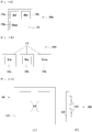
- FIGs. 1A and 1B are views showing conventional light emitting device packages.
- the light emitting devices 150a, 150b and 150c are arranged on a substrate 110 and spaced apart from one another by a prescribed distance.
- the light emitting devices 150a, 150b and 150c may emit light of the same wavelength range or light of different wavelength ranges.
- three light emitting devices 150a, 150b and 150c to emit red, green and blue light of different wavelength ranges respectively may be arranged on a single substrate 110.
- the three light emitting devices 150a, 150b and 150c to emit red, green and blue light of different wavelength ranges may be arranged respectively on different substrates 110.
- the three light emitting devices 150a, 150b and 150c may emit light of different wavelength ranges from active layers thereof, or may include different kinds of fluorescent substances disposed on the active layers that emit light of the same wavelength range.
- FIG. 2A is a view showing a conventional light emitting device package.
- the light emitting devices 150 are arranged on a substrate 110 and spaced apart from one another by a prescribed distance.
- the respective light emitting devices 150 may emit light of the same wavelength range or light of different wavelength ranges.
- FIG. 2B is a view showing a conventional light source module.
- a lens 180 may be located in front of the light emitting device package 100 and serve to change a progress path of light emitted from the respective light emitting devices 150.
- the lens 180 may be an aspheric lens that directly transmits light from the light emitting devices 150 and, thus, the shape of light sources of the light emitting devices 150 may be important.
- light sources of light emitting devices typically have a rectangular or square shape and are limited in the emission shape of light to be transmitted outward.
- the present invention provides a light emitting diode package for vehicles according to claim 1, , which allows to achieve an increased degree of freedom in terms of arrangement of light sources, diversification in the emission shape of light to be transmitted outward from light sources and reduced manufacturing costs.
- each layer may be exaggerated, omitted or schematically illustrated for clarity and convenience.
- the size of each constituent element does not wholly reflect an actual size thereof.
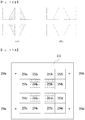
- FIG. 3 is a view schematically showing a configuration of light emitting cells in a light emitting device package according to an example not forming part of the present invention.
- a single light emitting device may be divided into a plurality of light emitting cells, e.g., four light emitting cells W, R, G and Y as exemplarily shown in FIG. 3 , and the respective light emitting cells W, R, G and Y may be separated from one another with an insulating layer interposed between light emitting cells W, R, G and Y.
- the aforementioned light emitting cells may be formed by growing a single light emitting structure and dividing the same by etching. Since the single light emitting structure emits light of the same wavelength range, the respective light emitting cells may be respectively provided with fluorescent substances to emit light of different wavelength ranges.
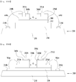
- FIG. 4 is a view showing an example of a light emitting device package not forming part of the present invention.
- the light emitting device package 200 includes a single light emitting device disposed on a package body, such as, e.g. a substrate 210.
- a plurality of light emitting devices may be disposed, and at least one light emitting device may be divided into a plurality of light emitting cells.
- a single light emitting device may be divided into four light emitting cells 250a to 250d and the respective light emitting cells may emit red, green, white and yellow light of different wavelength ranges.
- a light emitting structure emits light of the same wavelength range and the respective light emitting cells 250a to 250d are provided with different fluorescent substances.
- the fluorescent substances may emit light of different wavelength ranges when excited by the above-described light of the same wavelength range and, in turn, the respective light emitting cells 250a to 250d may emit light of different wavelength ranges.
- the first light emitting cell 250a may be provided with a fluorescent substance that is excited by light of the blue wavelength range to emit light of a wavelength range between 550 nm and 565 nm
- the second light emitting cell 250b may be provided with a fluorescent substance that is excited by light of the blue wavelength range to emit light of a wavelength range between 620 nm and 650 nm
- the third light emitting cell 250c may be provided with a fluorescent substance that is excited by light of the blue wavelength range to emit light of a wavelength range between 510 nm and 540 nm
- the fourth light emitting cell 250d may be provided with a fluorescent substance that is excited by light of the blue wavelength range to emit light of a wavelength range between 590 nm and 600 nm.
- the light emitting cells 250a to 250d are separated from each other and spaced apart from one another by a predetermined distance d1.
- the predetermined distance d1 may be within a range of 10 ⁇ m to 50 ⁇ m. An excessively great distance has substantially less difference in comparison with manufacturing respective light emitting cells using separate light emitting devices, and an excessively small distance may cause difficulty in separation of light emitting cells during etching.
- FIGs. 5A and 5B are views showing examples of a configuration of light emitting cells in a light emitting structure of a light emitting device package not forming part of the present invention.
- FIG. 5A shows a vertical light emitting device and FIG. 5B shows a horizontal light emitting device, each light emitting device including a plurality of light emitting cells placed therein.
- FIGs. 5A and 5B may be vertical cross sectional views taken in direction A-A' of FIG. 4 .
- two light emitting cells 250b and 250d are separately disposed above a single conductive support substrate 240 that is, in turn, disposed on a substrate 210.
- the light emitting cells 250b and 250d are spaced apart from each other by a predetermined distance d1.
- a conductive bonding layer 242 and a second electrode 244 may be sequentially stacked on the conductive support substrate 240 and the light emitting cells 250b and 250d may be disposed on the second electrode 244.
- a first electrode 251b may be formed on one light emitting cell 250b.
- the first electrode 251b may be bonded to a first bonding pad 210b on the substrate 210 via a wire and a fluorescent substance 260b may be disposed on the light emitting cell 250b.
- the fluorescent substance 260b for example, may be a green fluorescent substance.
- a first electrode 251d may be formed on the other light emitting cell 250d.
- the first electrode 251d may be bonded to a first bonding pad 210d on the substrate 210 via a wire and a fluorescent substance 260d may be disposed on the light emitting cell 250d.
- the fluorescent substance 260d may be a yellow fluorescent substance.
- the first electrode may be formed over a first conductive semiconductor layer in a light emitting structure.
- two light emitting cells 250b and 250d are separately disposed on an insulating substrate 230 formed of sapphire or the like that is, in turn, disposed on a substrate 210.
- the light emitting cells 250b and 250d are spaced apart from each other by a predetermined distance d1.
- One light emitting cell 250b may be subjected, at a region thereof, to mesa-etching such that a first electrode 251b is disposed on the mesa-etched region, and a second electrode 252b may be formed on the light emitting cell 250b.
- the first electrode 251b may be bonded to a first bonding pad 210b on the substrate 210 via a wire
- the second electrode 252b may be bonded to a second bonding pad (not shown) on the substrate 210 via a wire
- a fluorescent substance 260b may be disposed on the light emitting cell 250b.
- the fluorescent substance 260b for example, may be a green fluorescent substance.
- the other light emitting cell 250d may be subjected, at a region thereof, to mesa-etching such that a first electrode 251d is formed on the mesa-etched region, and a second electrode 252d may be formed on the light emitting cell 250d.
- the first electrode 251d may be bonded to a first bonding pad 210d on the substrate 210 via a wire
- the second electrode 252d may be bonded to a second bonding pad (not shown) on the substrate 210 via a wire
- a fluorescent substance 260d may be disposed on the light emitting cell 250d.
- the fluorescent substance 260d for example, may be a yellow fluorescent substance.
- each light emitting cell is mesa-etched such that a second conductive semiconductor layer, an active layer and a portion of a first conductive semiconductor layer are etched to expose a portion of the first conductive semiconductor layer. Then, a second electrode and a first electrode may be disposed respectively on the second conductive semiconductor layer in an unetched region and the exposed first conductive semiconductor layer in the etched region of the light emitting cell.
- the first electrodes and the second electrodes, connected to the respective light emitting cells may be connected in parallel or may be independent of each other, thereby allowing the respective light emitting cells to be driven individually.
- the fluorescent substances may take the form of a conformal coating or a film.
- the light emitting device package according to the present example in which a plurality of light emitting cells is formed in a single light emitting device may emit various colors of light within a narrow space and employ a reduced number of light emitting devices, which, in turn, enables change of design in a limited space on the substrate and reduction of manufacturing costs.
- FIGs. 6A and 6B are views showing examples of a manufacturing process of light emitting cells in a light emitting structure of a light emitting device package not forming part of the present invention.
- a light emitting structure including a first conductive semiconductor layer, an active layer and a second conductive semiconductor layer may be grown and then divided into a plurality of light emitting cells via etching that will be described below.
- FIG. 6A shows division of light emitting cells in a vertical light emitting device.
- a light emitting structure 250 may be disposed on a conductive semiconductor substrate 240 that is in turn disposed on a substrate 210.
- the light emitting structure 250 may be selectively etched using a mask to thereby be divided into two light emitting cells 250b and 250d as exemplarily shown in the right side of the drawing.
- the light emitting structure 250 may be grown on a growth substrate (not shown) and mounted on the conductive support substrate 240. After the growth substrate is removed via LLO or the like, the light emitting structure 250 is divided into unit cells by etching and formation of electrodes, application of fluorescent substances and the like may be performed.
- the conductive support substrate 240 is mounted on the substrate 210 and wire bonding and the like may be performed.
- the light emitting structure 250 is divided into unit cells and formation of electrodes, application of fluorescent substances and the like may be performed.
- FIG. 6B shows division of light emitting cells in a horizontal light emitting device.
- a light emitting structure 250 may be disposed on an insulating substrate 230 and selectively etched using a mask or via mesa-etching to thereby be divided into two light emitting cells 250b and 250d as exemplarily shown in the right side of the drawing. Subsequently, some regions of the respective light emitting cells 250b and 250d may be mesa-etched.
- wire bonding and the like may be performed.
- the above-described etching process may be performed.
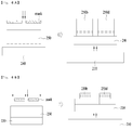
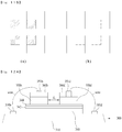
- FIG. 7 is a view showing an embodiment of an arrangement of light emitting diode package for vehicles according to the present invention.
- a light emitting diode package includes eight light emitting diode devices 301 to 308 disposed on a substrate 310 and the light emitting diode devices 301 to 308 respectively include two light emitting diode cells 301a/301b to 308a/308b.
- the first light emitting diode cells 301a to 308a emit red light R and second light emitting diode cells 301b to 308b emit yellow light Y.
- the red light R and yellow light Y is acquired via combination of light emitted from an active layer in each light emitting diode device and light emitted from an excited fluorescent substance on the light emitting diode cells.
- FIG. 7 shows the first light emitting diode cells 301a to 308a and the second light emitting diode cells 301b to 308b as coming into contact with each other
- the first light emitting diode cells 301a to 308a and the second light emitting diode cells 301b to 308b of the respective light emitting diode devices 301 to 308, in accordance with the present invention are spaced apart from each other by a distance d1 of 10 ⁇ m to 50 ⁇ m.
- first light emitting diode cells 301a to 308a and the second light emitting diode cells 301b to 308b are driven independently of each other. As shown in FIG. 7 , the first light emitting diode cells 301a to 308a are connected to one line a and the second light emitting diode cells 301b to 308b are connected to the other line b.
- the lighting device for vehicles which includes the light emitting diode package shown in FIG. 7 , more particularly, a rear lamp for vehicles may emit red light using the eight first light emitting cells 301a to 308a upon receiving current applied to the line a.
- the red light may indicate a break signal.
- the rear lamp may emit yellow light using the eight second light emitting cells 301b to 308b upon receiving current applied to the line b.
- the yellow light may indicate a break signal.
- each light emitting device disposed on a substrate may be divided into a plurality of light emitting cells and fluorescent substances to emit light of a plurality of wavelength ranges may be disposed on the respective light emitting cells.
- the single light emitting device may emit light of the different wavelength ranges.
- the light emitting cells are arranged in any of various shapes rather than a rectangular or square shape, thus achieving a light source having any of various shapes.
- FIGs. 8 and 9 are views showing examples of a light emitting device package not forming part of the present invention.
- the light emitting device package according to the example includes a first light emitting device to a fourth light emitting device 250a, 250b, 250c and 250d disposed on a substrate 210.
- the first light emitting device 250a may include four light emitting cells 251a, 252a, 253a and 254a
- the second light emitting device 250b may include four light emitting cells 251b, 252b, 253b and 254b
- the third light emitting device 250c may include four light emitting cells 251c, 252c, 253c and 254c
- the fourth light emitting device 250d may include four light emitting cells 251d, 252d, 253d and 254d.
- a first fluorescent substance may be disposed on one light emitting cell 251a, 252b, 253c or 254d of each of the first to fourth light emitting devices 250a, 250b, 250c and 250d, and a second fluorescent substance may be disposed on the other light emitting cells.
- the first fluorescent substance and the second fluorescent substance are adapted to emit light of a first wavelength range and light of a second wavelength range when excited by light emitted from active layers of the respective light emitting devices 250a, 250b, 250c and 250d.
- the light emitting cells provided with the first fluorescent substance may outwardly emit a mixture of light emitted from the active layer and light of the first wavelength range
- the light emitting cells provided with the second fluorescent substance may outwardly emit a mixture of light emitted from the active layer and light of the second wavelength range.
- the light emitting device package according to the example may include a first light emitting device to a ninth light emitting device 250a to 250i disposed on a substrate 210, and the light emitting devices 250a to 250i may respectively include four light emitting cells.
- the light emitting cells of the respective light emitting devices 250a to 250i may be sorted into two kinds of light emitting cells to emit light of different wavelength ranges. Similar to the light emitting device package according to the above-described example, different fluorescent substances to emit light of different wavelength ranges may be disposed on the respective light emitting cells.
- some of the light emitting cells may be provided with the fluorescent substance and the other light emitting cells may be provided with no fluorescent substance.
- the light emitting cells may be spaced apart from one another by different distances. That is, a distance between the light emitting cells of the same light emitting device may be less than a distance between the light emitting cells of the neighboring light emitting devices.
- the fluorescent substances on the respective light emitting cells are excited by the light emitted from the active layers, thereby emitting light of a first wavelength range and light of a second wavelength range.
- the light emitting cells included in a single light emitting device may outwardly emit two kinds of light.
- light emitted from the entire light emitting device package may indicate a specific shape of light source.
- light emitted from the entire light emitting device package may be seen in the shape of number "12". Accordingly, as light emitting devices in a light emitting device package are respectively divided into a plurality of light emitting cells and different kinds of fluorescent substances are disposed on the light emitting cells, one light emitting device or the light emitting device package may have any of various shapes rather than a rectangular or square shape, and these shapes may indicate any of specific emblems, such as symbols, letters, numbers or the like.
- FIGs. 10A and 10B are views showing on and off states of an example of a light emitting device package not forming part of the present invention.
- the light emitting device package according to the example is similar to the light emitting device package shown in FIG. 8 based on the fact that a single light emitting device includes four light emitting cells, in the present example, all of the light emitting cells may not be identical to one another in terms of an area and/or a shape in comparison with FIGs. 8 and 9 in which all of the light emitting cells have the same area and shape.
- the light emitting device package according to the example includes first to fourth light emitting devices 250a, 250b, 250c and 250d on a substrate 210.
- the first light emitting device 250a may include two square light emitting cells 251a and 253a and two triangular light emitting cells 252a and 254a
- the second light emitting device 250b may include two square light emitting cells 252b and 253b and two triangular light emitting cells 251b and 254b
- the third light emitting device 250c may include two square light emitting cells 251c and 253c and two triangular light emitting cells 252c and 254c
- the fourth light emitting device 250d may include two square light emitting cells 251d and 252d and two triangular light emitting cells 253d and 254d.
- One light emitting cell 254a in the first light emitting device 250a, one light emitting cell 254b in the second light emitting device 250b, one light emitting cell 254c in the third light emitting device 250c and one light emitting cell 254d in the fourth light emitting device 250d are provided with a fluorescent substance that is a different kind from that of the other light emitting cells. Different kinds of fluorescent substances emit light of different wavelength ranges when excited by light emitted from active layers of light emitting devices. Thus, a wavelength of light emitted from the four light emitting cells 254a, 254b, 254c and 254d differs from a wavelength of light emitted from the other light emitting cells.
- four light emitting devices may indicate emblems corresponding to a leftward arrow and/or a rightward arrow upon receiving current.
- direction indicating emblems may be indicated.
- FIG. 10B the case of supplying no current to the light emitting devices is shown.
- FIGs. 11A and 11B are views showing on and off states of an example of a light emitting device package not forming part of the present invention.
- the light emitting device package according to the example is similar to that of the above-described example, but has a difference that one light emitting device includes four light emitting cells having the same area and shape.
- a first light emitting device 250a may include four light emitting cells 251a, 252a, 253a and 254a
- a second light emitting device 250b may include four light emitting cells 251b, 252b, 253b and 254b
- a third light emitting device 250c may include four light emitting cells 251c, 252c, 253c and 254c
- a fourth light emitting device 250d may include four light emitting cells 251d, 252d, 253d and 254d.
- a first fluorescent substance may be disposed on one light emitting cell 254a, 253b, 252c or 251d of each of the first light emitting device to the fourth light emitting device 250a, 250b, 250c and 250d, and a second fluorescent substance may be disposed on the other light emitting cells.
- the first fluorescent substance and the second fluorescent substance respectively emit light of a first wavelength range and light of a second wavelength range when excited by light emitted from active layers of the respective light emitting devices 250a, 250b, 250c and 250d.
- the light emitting cells provided with the first fluorescent substance may outwardly emit a mixture of light emitted from the active layer and light of the first wavelength range
- the light emitting cells provided with the second fluorescent substance may outwardly emit a mixture of light emitted from the active layer and light of the second wavelength range.
- center four light emitting cells and peripheral light emitting cells indicate different colors when current is supplied to the light emitting devices and, thus, the light emitting devices may constitute, e.g., a signal lamp for a specific emblem or for a specific purpose.
- the light emitting devices may constitute, e.g., a signal lamp for a specific emblem or for a specific purpose.
- a brake lamp and a signal lamp may be integrated to be selectively or wholly turned on or off.
- FIG. 11B the case of supplying no current to the light emitting devices is shown.
- FIGs. 12A and 12B are views showing different configurations of light emitting cells in a light emitting structure of a light emitting device package.
- FIG. 12A shows a vertical light emitting device and FIG. 12B shows a horizontal light emitting device, each light emitting device including a plurality of light emitting cells placed therein.
- FIGs. 12A and 12B may be vertical cross sectional views taken along direction A-A' of FIG. 4 .
- two light emitting cells 350b and 350d are separately disposed above a single conductive support substrate 340 that is in turn disposed on a substrate 310.
- the light emitting cells 350b and 350d are spaced apart from each other by a predetermined distance d1.
- a conductive bonding layer 342 and a second electrode 344 may be disposed on the conductive support substrate 340 and the light emitting cells 350b and 350d may be disposed on the second electrode 344.
- the predetermined distance d1 may be within a range of 10 ⁇ m to 50 ⁇ m. An excessively great distance has substantially less difference in comparison with manufacturing respective light emitting cells using separate light emitting devices, and an excessively small distance may cause difficulty in separation of light emitting cells during etching.
- a first electrode 351b may be formed on one light emitting cell 350b.
- the first electrode 351b may be bonded to a first bonding pad 310b on the substrate 310 via a wire and a fluorescent substance 360b may be disposed on the light emitting cell 350b.
- the fluorescent substance 360b for example, may be a green fluorescent substance.
- a first electrode 351d may be formed on the other light emitting cell 350d.
- the first electrode 351d may be bonded to a first bonding pad 310d on the substrate 310 via a wire and a fluorescent substance 360d may be disposed on the light emitting cell 350d.
- the fluorescent substance 360d may be a yellow fluorescent substance.
- the first electrode may be formed on a first conductive semiconductor layer in a light emitting structure.
- two light emitting cells 350b and 350d are separately disposed on an insulating substrate 330 formed of sapphire or the like that is in turn disposed on a substrate 310.
- the light emitting cells 350b and 350d are spaced apart from each other by a predetermined distance d1.
- One light emitting cell 350b may be subjected, at a region thereof, to mesa-etching such that a first electrode 351b is formed on the mesa-etched region, and a second electrode 352b may be formed on the light emitting cell 350b.
- the first electrode 351b may be bonded to a first bonding pad 310b on the substrate 310 via a wire
- the second electrode 352b may be bonded to a second bonding pad (not shown) on the substrate 310 via a wire
- a fluorescent substance 360b may be disposed on the light emitting cell 350b.
- the fluorescent substance 360b for example, may be a green fluorescent substance.
- the other light emitting cell 350d may be subjected, at a region thereof, to mesa-etching such that a first electrode 351d is formed on the mesa-etched region, and a second electrode 352d may be formed on the light emitting cell 350d.
- the first electrode 351d may be bonded to a first bonding pad 310d on the substrate 310 via a wire
- the second electrode 352d may be bonded to a second bonding pad (not shown) on the substrate 310 via a wire
- a fluorescent substance 360d may be disposed on the light emitting cell 350d.
- the fluorescent substance 360d for example, may be a yellow fluorescent substance.
- each light emitting cell is mesa-etched such that a second conductive semiconductor layer, an active layer and a portion of a first conductive semiconductor layer are etched to expose a portion of the first conductive semiconductor layer. Then, a second electrode and a first electrode may be disposed respectively on the second conductive semiconductor layer in an unetched region and the exposed first conductive semiconductor layer in the etched region of the light emitting cell.
- the first electrodes and the second electrodes, connected to the respective light emitting cells may be connected in parallel or may be independent of each other, thereby allowing the respective light emitting cells to be driven individually.
- the fluorescent substances may take the form of a conformal coating or a film.
- FIGs. 13A and 13B are views showing a manufacturing process of the light emitting cells shown in FIGs. 12A and 12B and may be identical to the example shown in FIGs. 6A and 6B .
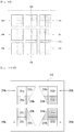
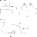
- FIG. 14 is a view showing an embodiment of a lighting device for vehicles containing a light emitting device package according to the present invention.
- a lighting device 400 for vehicles according to the embodiment may be configured in such a way that light emitted from a light emitting device module 401 having a light emitting device package is reflected by a reflector 402 and a shade 403 and then passes through a lens 404 to thereby be directed to the rear of a vehicle body.
- the light emitting device module 401 may include the above-described light emitting device package disposed on a board.
- light emitting devices in the light emitting device module may respectively include a plurality of light emitting cells and each light emitting device may emit light of two wavelength ranges.
- a light emitting device package in which a single light emitting device defines a plurality of light emitting cells may emit light of various colors within a narrow space.
- the light emitting device package may employ a reduced number of light emitting devices, which enables change of design in a limited space on the substrate and reduction of manufacturing costs.
- one light emitting device or the light emitting device package may have any of various shapes rather than a rectangular or square shape, and these shapes may indicate any of specific emblems, such as symbols, letters, numbers or the like.
Landscapes
- Engineering & Computer Science (AREA)
- General Engineering & Computer Science (AREA)
- Microelectronics & Electronic Packaging (AREA)
- Physics & Mathematics (AREA)
- Optics & Photonics (AREA)
- Led Device Packages (AREA)
- Led Devices (AREA)
- Non-Portable Lighting Devices Or Systems Thereof (AREA)
Applications Claiming Priority (2)
| Application Number | Priority Date | Filing Date | Title |
|---|---|---|---|
| KR1020130103831A KR102080776B1 (ko) | 2013-08-30 | 2013-08-30 | 발광소자 패키지 및 이를 포함하는 차량용 조명 장치 |
| KR20130103830A KR20150025797A (ko) | 2013-08-30 | 2013-08-30 | 발광소자 패키지 및 이를 포함하는 차량용 조명 장치 |
Publications (2)
| Publication Number | Publication Date |
|---|---|
| EP2843705A1 EP2843705A1 (en) | 2015-03-04 |
| EP2843705B1 true EP2843705B1 (en) | 2020-03-11 |
Family
ID=51417223
Family Applications (1)
| Application Number | Title | Priority Date | Filing Date |
|---|---|---|---|
| EP14182912.7A Active EP2843705B1 (en) | 2013-08-30 | 2014-08-29 | Light emitting diode package for vehicles |
Country Status (4)
| Country | Link |
|---|---|
| US (1) | US9269861B2 (enExample) |
| EP (1) | EP2843705B1 (enExample) |
| JP (1) | JP6713720B2 (enExample) |
| CN (1) | CN104425540A (enExample) |
Cited By (1)
| Publication number | Priority date | Publication date | Assignee | Title |
|---|---|---|---|---|
| EP4250362A4 (en) * | 2020-12-04 | 2024-10-23 | Seoul Viosys Co., Ltd. | MIXED COLOR ELECTROLUMINESCENT DEVICE |
Families Citing this family (10)
| Publication number | Priority date | Publication date | Assignee | Title |
|---|---|---|---|---|
| WO2016080768A1 (ko) * | 2014-11-18 | 2016-05-26 | 서울반도체 주식회사 | 발광 장치 및 이를 포함하는 차량용 램프 |
| US10170455B2 (en) * | 2015-09-04 | 2019-01-01 | PlayNitride Inc. | Light emitting device with buffer pads |
| TWI646706B (zh) | 2015-09-21 | 2019-01-01 | 隆達電子股份有限公司 | 發光二極體晶片封裝體 |
| US10219345B2 (en) * | 2016-11-10 | 2019-02-26 | Ledengin, Inc. | Tunable LED emitter with continuous spectrum |
| CN110707189B (zh) | 2017-02-08 | 2023-09-01 | 首尔半导体株式会社 | 发光模块 |
| KR102563894B1 (ko) | 2017-02-08 | 2023-08-10 | 서울반도체 주식회사 | 발광 다이오드 및 이를 포함하는 발광 모듈 |
| JP6986697B2 (ja) * | 2017-06-28 | 2021-12-22 | パナソニックIpマネジメント株式会社 | 紫外線発光素子 |
| US10340308B1 (en) | 2017-12-22 | 2019-07-02 | X Development Llc | Device with multiple vertically separated terminals and methods for making the same |
| US11362073B2 (en) | 2019-02-08 | 2022-06-14 | Seoul Viosys Co., Ltd. | Light emitting device including multiple transparent electrodes for display and display apparatus having the same |
| KR102642606B1 (ko) | 2019-05-30 | 2024-03-05 | 삼성디스플레이 주식회사 | 윈도우 및 윈도우의 제조 방법 |
Citations (2)
| Publication number | Priority date | Publication date | Assignee | Title |
|---|---|---|---|---|
| WO2000024064A1 (en) * | 1998-10-21 | 2000-04-27 | Sarnoff Corporation | A method and apparatus for performing wavelength-conversion using phosphors with light emitting diodes |
| EP2187442A2 (en) * | 2008-11-18 | 2010-05-19 | LG Innotek Co., Ltd. | Light emitting device and light emitting device package having the same |
Family Cites Families (22)
| Publication number | Priority date | Publication date | Assignee | Title |
|---|---|---|---|---|
| JPH09330604A (ja) * | 1996-06-06 | 1997-12-22 | Koito Mfg Co Ltd | 車輌用標識灯 |
| JP3691951B2 (ja) * | 1998-01-14 | 2005-09-07 | 東芝電子エンジニアリング株式会社 | 窒化ガリウム系化合物半導体発光素子 |
| US6737801B2 (en) * | 2000-06-28 | 2004-05-18 | The Fox Group, Inc. | Integrated color LED chip |
| JP2004055742A (ja) * | 2002-07-18 | 2004-02-19 | Sanyo Electric Co Ltd | 発光素子及びそれを備えた発光素子アレイ |
| WO2005022654A2 (en) | 2003-08-28 | 2005-03-10 | Matsushita Electric Industrial Co.,Ltd. | Semiconductor light emitting device, light emitting module, lighting apparatus, display element and manufacturing method of semiconductor light emitting device |
| EP2280430B1 (en) * | 2005-03-11 | 2020-01-01 | Seoul Semiconductor Co., Ltd. | LED package having an array of light emitting cells coupled in series |
| JP2009224431A (ja) * | 2008-03-14 | 2009-10-01 | Nichia Corp | 半導体装置 |
| US8354665B2 (en) | 2008-08-19 | 2013-01-15 | Lattice Power (Jiangxi) Corporation | Semiconductor light-emitting devices for generating arbitrary color |
| KR101562774B1 (ko) | 2009-02-24 | 2015-10-22 | 서울반도체 주식회사 | 발광모듈 |
| TWI381556B (zh) * | 2009-03-20 | 2013-01-01 | 億光電子工業股份有限公司 | 發光二極體封裝結構及其製作方法 |
| US8455904B2 (en) * | 2009-04-20 | 2013-06-04 | 3M Innovative Properties Company | Non-radiatively pumped wavelength converter |
| KR101007077B1 (ko) * | 2009-11-06 | 2011-01-10 | 엘지이노텍 주식회사 | 발광소자, 발광소자 패키지 및 그 제조방법 |
| EP2367203A1 (en) | 2010-02-26 | 2011-09-21 | Samsung LED Co., Ltd. | Semiconductor light emitting device having multi-cell array and method for manufacturing the same |
| US8604498B2 (en) * | 2010-03-26 | 2013-12-10 | Tsmc Solid State Lighting Ltd. | Single phosphor layer photonic device for generating white light or color lights |
| JP2012019104A (ja) | 2010-07-08 | 2012-01-26 | Mitsubishi Chemicals Corp | 発光装置 |
| KR101909299B1 (ko) * | 2010-10-27 | 2018-10-17 | 루미리즈 홀딩 비.브이. | 발광 디바이스의 제조를 위한 적층 지지막 및 그 제조 방법 |
| EP2660882B1 (en) * | 2010-12-28 | 2018-10-03 | Nichia Corporation | Semiconductor light-emitting device |
| KR101748334B1 (ko) * | 2011-01-17 | 2017-06-16 | 삼성전자 주식회사 | 백색 발광 소자의 제조 방법 및 제조 장치 |
| JP2012216712A (ja) * | 2011-03-28 | 2012-11-08 | Nitto Denko Corp | 発光ダイオード装置の製造方法および発光ダイオード素子 |
| US20130075769A1 (en) | 2011-09-22 | 2013-03-28 | Ledengin, Inc. | Selection of phosphors and leds in a multi-chip emitter for a single white color bin |
| TW201320406A (zh) * | 2011-11-11 | 2013-05-16 | 東貝光電科技股份有限公司 | 提升混光效果之白光二極體封裝改良結構 |
| KR102003001B1 (ko) | 2013-03-13 | 2019-07-23 | 엘지이노텍 주식회사 | 발광 모듈 |
-
2014
- 2014-08-28 JP JP2014173374A patent/JP6713720B2/ja active Active
- 2014-08-29 US US14/472,514 patent/US9269861B2/en active Active
- 2014-08-29 CN CN201410437156.6A patent/CN104425540A/zh active Pending
- 2014-08-29 EP EP14182912.7A patent/EP2843705B1/en active Active
Patent Citations (2)
| Publication number | Priority date | Publication date | Assignee | Title |
|---|---|---|---|---|
| WO2000024064A1 (en) * | 1998-10-21 | 2000-04-27 | Sarnoff Corporation | A method and apparatus for performing wavelength-conversion using phosphors with light emitting diodes |
| EP2187442A2 (en) * | 2008-11-18 | 2010-05-19 | LG Innotek Co., Ltd. | Light emitting device and light emitting device package having the same |
Cited By (2)
| Publication number | Priority date | Publication date | Assignee | Title |
|---|---|---|---|---|
| EP4250362A4 (en) * | 2020-12-04 | 2024-10-23 | Seoul Viosys Co., Ltd. | MIXED COLOR ELECTROLUMINESCENT DEVICE |
| US12604561B2 (en) | 2020-12-04 | 2026-04-14 | Seoul Viosys Co., Ltd. | Mixed color light emitting device |
Also Published As
| Publication number | Publication date |
|---|---|
| US9269861B2 (en) | 2016-02-23 |
| US20150062949A1 (en) | 2015-03-05 |
| JP2015050461A (ja) | 2015-03-16 |
| EP2843705A1 (en) | 2015-03-04 |
| CN104425540A (zh) | 2015-03-18 |
| JP6713720B2 (ja) | 2020-06-24 |
Similar Documents
| Publication | Publication Date | Title |
|---|---|---|
| EP2843705B1 (en) | Light emitting diode package for vehicles | |
| CN111052387B (zh) | 高密度像素化的led芯片和芯片阵列装置及制造方法 | |
| TWI610465B (zh) | 發光二極體組件及製作方法 | |
| CN105378952B (zh) | 发光器件封装件及其制造方法以及包含该发光器件封装件的车灯和背光单元 | |
| US10177286B2 (en) | Light emitting element package having three regions | |
| EP3239592A1 (en) | Light emitting device and vehicular lamp comprising same | |
| US20250133885A1 (en) | Vehicular display element having a high density led array | |
| US10164159B2 (en) | Light-emitting diode package and method of manufacturing the same | |
| US20150014708A1 (en) | Package for light emitting and receiving devices | |
| KR20150144048A (ko) | 발광 소자 및 이를 포함하는 발광소자 패키지 | |
| CN112136219A (zh) | 照明模块及包括其的照明装置 | |
| EP2744001A2 (en) | Light emitting device package | |
| EP2860778A1 (en) | Multi-area light emitting diode, light emitting device package including the diode and lighting apparatus including the package | |
| KR20120133264A (ko) | 발광소자 렌즈, 이를 포함하는 발광소자 모듈 및 이를 이용한 발광소자 모듈의 제조방법 | |
| KR102886339B1 (ko) | 조명 모듈 및 이를 구비한 조명 장치 | |
| KR20120026343A (ko) | 발광소자 패키지 | |
| KR102531109B1 (ko) | 발광 소자 및 이를 구비한 조명 모듈 | |
| KR102080776B1 (ko) | 발광소자 패키지 및 이를 포함하는 차량용 조명 장치 | |
| KR20150025797A (ko) | 발광소자 패키지 및 이를 포함하는 차량용 조명 장치 | |
| US20190280162A1 (en) | Light-emitting diode package and method of manufacturing the same | |
| US9257618B2 (en) | LED package and method of manufacturing the same | |
| US20070045648A1 (en) | Package structure of light emitting diode | |
| KR102584543B1 (ko) | 조명 모듈 및 이를 구비한 조명 장치 | |
| KR100609970B1 (ko) | 발광 소자 실장용 기판 및 그의 제조 방법, 그를 이용한패키지 | |
| US8658443B2 (en) | Method for manufacturing light emitting device |
Legal Events
| Date | Code | Title | Description |
|---|---|---|---|
| 17P | Request for examination filed |
Effective date: 20140829 |
|
| AK | Designated contracting states |
Kind code of ref document: A1 Designated state(s): AL AT BE BG CH CY CZ DE DK EE ES FI FR GB GR HR HU IE IS IT LI LT LU LV MC MK MT NL NO PL PT RO RS SE SI SK SM TR |
|
| AX | Request for extension of the european patent |
Extension state: BA ME |
|
| PUAI | Public reference made under article 153(3) epc to a published international application that has entered the european phase |
Free format text: ORIGINAL CODE: 0009012 |
|
| RBV | Designated contracting states (corrected) |
Designated state(s): AL AT BE BG CH CY CZ DE DK EE ES FI FR GB GR HR HU IE IS IT LI LT LU LV MC MK MT NL NO PL PT RO RS SE SI SK SM TR |
|
| RAP1 | Party data changed (applicant data changed or rights of an application transferred) |
Owner name: LG INNOTEK CO., LTD. |
|
| STAA | Information on the status of an ep patent application or granted ep patent |
Free format text: STATUS: EXAMINATION IS IN PROGRESS |
|
| 17Q | First examination report despatched |
Effective date: 20180718 |
|
| GRAP | Despatch of communication of intention to grant a patent |
Free format text: ORIGINAL CODE: EPIDOSNIGR1 |
|
| STAA | Information on the status of an ep patent application or granted ep patent |
Free format text: STATUS: GRANT OF PATENT IS INTENDED |
|
| RIC1 | Information provided on ipc code assigned before grant |
Ipc: H01L 25/075 20060101ALN20190821BHEP Ipc: H01L 27/15 20060101AFI20190821BHEP Ipc: H01L 33/50 20100101ALN20190821BHEP |
|
| INTG | Intention to grant announced |
Effective date: 20190919 |
|
| GRAS | Grant fee paid |
Free format text: ORIGINAL CODE: EPIDOSNIGR3 |
|
| GRAA | (expected) grant |
Free format text: ORIGINAL CODE: 0009210 |
|
| STAA | Information on the status of an ep patent application or granted ep patent |
Free format text: STATUS: THE PATENT HAS BEEN GRANTED |
|
| AK | Designated contracting states |
Kind code of ref document: B1 Designated state(s): AL AT BE BG CH CY CZ DE DK EE ES FI FR GB GR HR HU IE IS IT LI LT LU LV MC MK MT NL NO PL PT RO RS SE SI SK SM TR |
|
| REG | Reference to a national code |
Ref country code: GB Ref legal event code: FG4D |
|
| REG | Reference to a national code |
Ref country code: CH Ref legal event code: EP |
|
| REG | Reference to a national code |
Ref country code: AT Ref legal event code: REF Ref document number: 1244225 Country of ref document: AT Kind code of ref document: T Effective date: 20200315 |
|
| REG | Reference to a national code |
Ref country code: IE Ref legal event code: FG4D |
|
| REG | Reference to a national code |
Ref country code: DE Ref legal event code: R096 Ref document number: 602014062086 Country of ref document: DE |
|
| REG | Reference to a national code |
Ref country code: NL Ref legal event code: FP |
|
| PG25 | Lapsed in a contracting state [announced via postgrant information from national office to epo] |
Ref country code: FI Free format text: LAPSE BECAUSE OF FAILURE TO SUBMIT A TRANSLATION OF THE DESCRIPTION OR TO PAY THE FEE WITHIN THE PRESCRIBED TIME-LIMIT Effective date: 20200311 Ref country code: NO Free format text: LAPSE BECAUSE OF FAILURE TO SUBMIT A TRANSLATION OF THE DESCRIPTION OR TO PAY THE FEE WITHIN THE PRESCRIBED TIME-LIMIT Effective date: 20200611 Ref country code: RS Free format text: LAPSE BECAUSE OF FAILURE TO SUBMIT A TRANSLATION OF THE DESCRIPTION OR TO PAY THE FEE WITHIN THE PRESCRIBED TIME-LIMIT Effective date: 20200311 |
|
| PG25 | Lapsed in a contracting state [announced via postgrant information from national office to epo] |
Ref country code: HR Free format text: LAPSE BECAUSE OF FAILURE TO SUBMIT A TRANSLATION OF THE DESCRIPTION OR TO PAY THE FEE WITHIN THE PRESCRIBED TIME-LIMIT Effective date: 20200311 Ref country code: BG Free format text: LAPSE BECAUSE OF FAILURE TO SUBMIT A TRANSLATION OF THE DESCRIPTION OR TO PAY THE FEE WITHIN THE PRESCRIBED TIME-LIMIT Effective date: 20200611 Ref country code: GR Free format text: LAPSE BECAUSE OF FAILURE TO SUBMIT A TRANSLATION OF THE DESCRIPTION OR TO PAY THE FEE WITHIN THE PRESCRIBED TIME-LIMIT Effective date: 20200612 Ref country code: SE Free format text: LAPSE BECAUSE OF FAILURE TO SUBMIT A TRANSLATION OF THE DESCRIPTION OR TO PAY THE FEE WITHIN THE PRESCRIBED TIME-LIMIT Effective date: 20200311 Ref country code: LV Free format text: LAPSE BECAUSE OF FAILURE TO SUBMIT A TRANSLATION OF THE DESCRIPTION OR TO PAY THE FEE WITHIN THE PRESCRIBED TIME-LIMIT Effective date: 20200311 |
|
| REG | Reference to a national code |
Ref country code: LT Ref legal event code: MG4D |
|
| PG25 | Lapsed in a contracting state [announced via postgrant information from national office to epo] |
Ref country code: EE Free format text: LAPSE BECAUSE OF FAILURE TO SUBMIT A TRANSLATION OF THE DESCRIPTION OR TO PAY THE FEE WITHIN THE PRESCRIBED TIME-LIMIT Effective date: 20200311 Ref country code: SM Free format text: LAPSE BECAUSE OF FAILURE TO SUBMIT A TRANSLATION OF THE DESCRIPTION OR TO PAY THE FEE WITHIN THE PRESCRIBED TIME-LIMIT Effective date: 20200311 Ref country code: RO Free format text: LAPSE BECAUSE OF FAILURE TO SUBMIT A TRANSLATION OF THE DESCRIPTION OR TO PAY THE FEE WITHIN THE PRESCRIBED TIME-LIMIT Effective date: 20200311 Ref country code: CZ Free format text: LAPSE BECAUSE OF FAILURE TO SUBMIT A TRANSLATION OF THE DESCRIPTION OR TO PAY THE FEE WITHIN THE PRESCRIBED TIME-LIMIT Effective date: 20200311 Ref country code: PT Free format text: LAPSE BECAUSE OF FAILURE TO SUBMIT A TRANSLATION OF THE DESCRIPTION OR TO PAY THE FEE WITHIN THE PRESCRIBED TIME-LIMIT Effective date: 20200805 Ref country code: SK Free format text: LAPSE BECAUSE OF FAILURE TO SUBMIT A TRANSLATION OF THE DESCRIPTION OR TO PAY THE FEE WITHIN THE PRESCRIBED TIME-LIMIT Effective date: 20200311 Ref country code: IS Free format text: LAPSE BECAUSE OF FAILURE TO SUBMIT A TRANSLATION OF THE DESCRIPTION OR TO PAY THE FEE WITHIN THE PRESCRIBED TIME-LIMIT Effective date: 20200711 Ref country code: LT Free format text: LAPSE BECAUSE OF FAILURE TO SUBMIT A TRANSLATION OF THE DESCRIPTION OR TO PAY THE FEE WITHIN THE PRESCRIBED TIME-LIMIT Effective date: 20200311 |
|
| REG | Reference to a national code |
Ref country code: AT Ref legal event code: MK05 Ref document number: 1244225 Country of ref document: AT Kind code of ref document: T Effective date: 20200311 |
|
| REG | Reference to a national code |
Ref country code: DE Ref legal event code: R097 Ref document number: 602014062086 Country of ref document: DE |
|
| PLBE | No opposition filed within time limit |
Free format text: ORIGINAL CODE: 0009261 |
|
| STAA | Information on the status of an ep patent application or granted ep patent |
Free format text: STATUS: NO OPPOSITION FILED WITHIN TIME LIMIT |
|
| PG25 | Lapsed in a contracting state [announced via postgrant information from national office to epo] |
Ref country code: IT Free format text: LAPSE BECAUSE OF FAILURE TO SUBMIT A TRANSLATION OF THE DESCRIPTION OR TO PAY THE FEE WITHIN THE PRESCRIBED TIME-LIMIT Effective date: 20200311 Ref country code: AT Free format text: LAPSE BECAUSE OF FAILURE TO SUBMIT A TRANSLATION OF THE DESCRIPTION OR TO PAY THE FEE WITHIN THE PRESCRIBED TIME-LIMIT Effective date: 20200311 Ref country code: DK Free format text: LAPSE BECAUSE OF FAILURE TO SUBMIT A TRANSLATION OF THE DESCRIPTION OR TO PAY THE FEE WITHIN THE PRESCRIBED TIME-LIMIT Effective date: 20200311 Ref country code: ES Free format text: LAPSE BECAUSE OF FAILURE TO SUBMIT A TRANSLATION OF THE DESCRIPTION OR TO PAY THE FEE WITHIN THE PRESCRIBED TIME-LIMIT Effective date: 20200311 |
|
| 26N | No opposition filed |
Effective date: 20201214 |
|
| PG25 | Lapsed in a contracting state [announced via postgrant information from national office to epo] |
Ref country code: PL Free format text: LAPSE BECAUSE OF FAILURE TO SUBMIT A TRANSLATION OF THE DESCRIPTION OR TO PAY THE FEE WITHIN THE PRESCRIBED TIME-LIMIT Effective date: 20200311 Ref country code: SI Free format text: LAPSE BECAUSE OF FAILURE TO SUBMIT A TRANSLATION OF THE DESCRIPTION OR TO PAY THE FEE WITHIN THE PRESCRIBED TIME-LIMIT Effective date: 20200311 |
|
| PG25 | Lapsed in a contracting state [announced via postgrant information from national office to epo] |
Ref country code: MC Free format text: LAPSE BECAUSE OF FAILURE TO SUBMIT A TRANSLATION OF THE DESCRIPTION OR TO PAY THE FEE WITHIN THE PRESCRIBED TIME-LIMIT Effective date: 20200311 |
|
| REG | Reference to a national code |
Ref country code: CH Ref legal event code: PL |
|
| PG25 | Lapsed in a contracting state [announced via postgrant information from national office to epo] |
Ref country code: LU Free format text: LAPSE BECAUSE OF NON-PAYMENT OF DUE FEES Effective date: 20200829 Ref country code: LI Free format text: LAPSE BECAUSE OF NON-PAYMENT OF DUE FEES Effective date: 20200831 Ref country code: CH Free format text: LAPSE BECAUSE OF NON-PAYMENT OF DUE FEES Effective date: 20200831 |
|
| REG | Reference to a national code |
Ref country code: BE Ref legal event code: MM Effective date: 20200831 |
|
| PG25 | Lapsed in a contracting state [announced via postgrant information from national office to epo] |
Ref country code: FR Free format text: LAPSE BECAUSE OF NON-PAYMENT OF DUE FEES Effective date: 20200831 |
|
| PG25 | Lapsed in a contracting state [announced via postgrant information from national office to epo] |
Ref country code: IE Free format text: LAPSE BECAUSE OF NON-PAYMENT OF DUE FEES Effective date: 20200829 Ref country code: BE Free format text: LAPSE BECAUSE OF NON-PAYMENT OF DUE FEES Effective date: 20200831 |
|
| PG25 | Lapsed in a contracting state [announced via postgrant information from national office to epo] |
Ref country code: TR Free format text: LAPSE BECAUSE OF FAILURE TO SUBMIT A TRANSLATION OF THE DESCRIPTION OR TO PAY THE FEE WITHIN THE PRESCRIBED TIME-LIMIT Effective date: 20200311 Ref country code: MT Free format text: LAPSE BECAUSE OF FAILURE TO SUBMIT A TRANSLATION OF THE DESCRIPTION OR TO PAY THE FEE WITHIN THE PRESCRIBED TIME-LIMIT Effective date: 20200311 Ref country code: CY Free format text: LAPSE BECAUSE OF FAILURE TO SUBMIT A TRANSLATION OF THE DESCRIPTION OR TO PAY THE FEE WITHIN THE PRESCRIBED TIME-LIMIT Effective date: 20200311 |
|
| PG25 | Lapsed in a contracting state [announced via postgrant information from national office to epo] |
Ref country code: MK Free format text: LAPSE BECAUSE OF FAILURE TO SUBMIT A TRANSLATION OF THE DESCRIPTION OR TO PAY THE FEE WITHIN THE PRESCRIBED TIME-LIMIT Effective date: 20200311 Ref country code: AL Free format text: LAPSE BECAUSE OF FAILURE TO SUBMIT A TRANSLATION OF THE DESCRIPTION OR TO PAY THE FEE WITHIN THE PRESCRIBED TIME-LIMIT Effective date: 20200311 |
|
| REG | Reference to a national code |
Ref country code: DE Ref legal event code: R079 Ref document number: 602014062086 Country of ref document: DE Free format text: PREVIOUS MAIN CLASS: H01L0027150000 Ipc: H10H0029140000 |
|
| PGFP | Annual fee paid to national office [announced via postgrant information from national office to epo] |
Ref country code: NL Payment date: 20250722 Year of fee payment: 12 |
|
| PGFP | Annual fee paid to national office [announced via postgrant information from national office to epo] |
Ref country code: DE Payment date: 20250721 Year of fee payment: 12 |
|
| PGFP | Annual fee paid to national office [announced via postgrant information from national office to epo] |
Ref country code: GB Payment date: 20250722 Year of fee payment: 12 |