EP2842598A1 - Elektrodenleitung oder Elektrodenabschnitt einer Elektrodenleitung - Google Patents
Elektrodenleitung oder Elektrodenabschnitt einer Elektrodenleitung Download PDFInfo
- Publication number
- EP2842598A1 EP2842598A1 EP14174639.6A EP14174639A EP2842598A1 EP 2842598 A1 EP2842598 A1 EP 2842598A1 EP 14174639 A EP14174639 A EP 14174639A EP 2842598 A1 EP2842598 A1 EP 2842598A1
- Authority
- EP
- European Patent Office
- Prior art keywords
- layer
- ceramic
- electrical
- layers
- metal layer
- Prior art date
- Legal status (The legal status is an assumption and is not a legal conclusion. Google has not performed a legal analysis and makes no representation as to the accuracy of the status listed.)
- Granted
Links
Images

Classifications
-
- A—HUMAN NECESSITIES
- A61—MEDICAL OR VETERINARY SCIENCE; HYGIENE
- A61N—ELECTROTHERAPY; MAGNETOTHERAPY; RADIATION THERAPY; ULTRASOUND THERAPY
- A61N1/00—Electrotherapy; Circuits therefor
- A61N1/02—Details
- A61N1/04—Electrodes
- A61N1/05—Electrodes for implantation or insertion into the body, e.g. heart electrode
- A61N1/056—Transvascular endocardial electrode systems
- A61N1/0565—Electrode heads
-
- H—ELECTRICITY
- H01—ELECTRIC ELEMENTS
- H01B—CABLES; CONDUCTORS; INSULATORS; SELECTION OF MATERIALS FOR THEIR CONDUCTIVE, INSULATING OR DIELECTRIC PROPERTIES
- H01B3/00—Insulators or insulating bodies characterised by the insulating materials; Selection of materials for their insulating or dielectric properties
- H01B3/02—Insulators or insulating bodies characterised by the insulating materials; Selection of materials for their insulating or dielectric properties mainly consisting of inorganic substances
- H01B3/12—Insulators or insulating bodies characterised by the insulating materials; Selection of materials for their insulating or dielectric properties mainly consisting of inorganic substances ceramics
-
- A—HUMAN NECESSITIES
- A61—MEDICAL OR VETERINARY SCIENCE; HYGIENE
- A61N—ELECTROTHERAPY; MAGNETOTHERAPY; RADIATION THERAPY; ULTRASOUND THERAPY
- A61N1/00—Electrotherapy; Circuits therefor
- A61N1/02—Details
- A61N1/04—Electrodes
- A61N1/05—Electrodes for implantation or insertion into the body, e.g. heart electrode
Definitions
- the invention relates to an elongated, implantable electrical lead having an end component at a longitudinal end of the electrical lead, the end component having at least one electrically conductive electrode surface electrically connected to the electrical lead.
- Such elongated, implantable electrical leads are known, for example, as electrode leads, such as stimulation electrode leads for implantable cardiac pacemakers or defibrillators.
- electrode leads typically have a proximal end with an electrical connection for connecting the electrode lead to a stimulation device, such as a pacemaker or defibrillator, and a distal end, typically with pacing or drain electrodes.
- a stimulation device such as a pacemaker or defibrillator
- an electrode head which forms a so-called tip electrode, is arranged at the distal end of an electrode line. At a short distance from the tip electrode and one or more ring electrodes can be provided.
- a stimulation electrode lead in which a metallic electrode is completely covered with an insulating layer.
- the metal of the electrode is called titanium
- the insulating layer on the electrode is titanium oxide with a layer thickness of the order of 1 ⁇ m.
- the metal of the electrode called aluminum and as the material of the insulating layer alumina.
- the invention has for its object to provide an alternative and improved as possible elongated electrical line of the type mentioned.
- this object is achieved in that the end component is a composite component which has at least one thin metal layer with a layer thickness of less than 1 ⁇ m.
- the thin metal layer is applied to electrically insulating material of the composite component.
- the thin metal layer is conductively connected to the electrical line and can therefore serve as an electrode surface, for example.
- the thin metal layer of almost at least one outer ceramic layer is almost completely or completely covered. Ideally, the thin metal layer is completely covered by the outer ceramic layer and electrically insulated from it by the latter.
- ceramic layers have the disadvantage that they can have small holes or imperfections, so-called pinholes, which can lead to the thin metal layer no longer being galvanically isolated from the environment of the composite component.
- an outer ceramic layer is that it is mechanically and chemically stable even at low thickness.
- a disadvantage is that ceramic layers are sensitive to electrical effects, such as spark erosion.
- small imperfections in the coating (the pinholes) lead to the formation of plasma channels under electrical stress. These plasma channels generate temperature peaks upon discharge, which result in damage to both the insulating layer and the carrier layer. Any damage of this nature may cause the electrode to malfunction during sensing or pacing.
- Simply increasing the layer thickness of the ceramic layer does not increase its long-term stability, since pinholes can not be closed or avoided by increasing the layer thickness.
- the inventors have recognized the disadvantages of ceramic insulating layers that face the fundamental advantages and counteract these by the fact that the metal layer is thin, so that in the case of a pinhole it evaporates as a result of the electrical discharge originally recognized as problematic, ie it is removed by spark erosion, so that the not remaining thin in the area of the pinhole Finally, metal layer is again completely electrically isolated from the environment of the composite component.
- Suitable layer thicknesses for the outer ceramic layer are preferably less than 10 ⁇ m and preferably greater than 1 ⁇ m.
- the metal layer preferably has a layer thickness of less than 100 nm, for example of the order of 10 nm.
- the electrically insulating material to which the thin metal layer is applied is preferably also a ceramic material.
- the electrically insulating material may be an insulating layer, which is applied to a metallic base body. If this insulating layer is likewise made of ceramic material-if it is therefore also a ceramic layer-it may, like the outer ceramic layer, have pinholes, which may result in the thin metal layer electrically contacting the metallic base body. However, it is extremely unlikely that a pinhole in the insulating layer under the thin metal layer is in the same place as a pinhole in the outer ceramic layer. This would be a pinhole in the electrically insulating material forming layer to which the metal layer is applied, not critical.
- multiple insulating layers and thin metal layers may alternately follow each other so that the composite component has a plurality of thin metal layers and intervening insulating layers, these insulating layers preferably being ceramic layers.
- the metal layer or the metal layers are preferably always thinner than the corresponding ceramic layers.
- a suitable material for the ceramic layer or the ceramic layers are, for example, silicon oxide or silicon carbide, or else a metal oxide, such as aluminum oxide or tantalum oxide.
- the thin metal layer may be, for example, a titanium layer.
- the material of an optionally present metallic base body may be titanium.
- the thin metal layer and in the case of several thin metal layers in particular the outermost thin metal layer, acts as an electrode surface, and the elongated Electrical lead is preferably a stimulation lead, especially for an implantable stimulation device, such as a pacemaker or defibrillator.
- the composite component of the elongated electrical line represents a basically also produced independently of the rest of the elongated electrical line object, which is also considered to be independently protectable.
- the electrical line according to the invention and in particular its composite component is preferably produced by a production method in which one or more ceramic layers are applied by means of physical vapor deposition (PVD). Additionally or alternatively, the manufacturing method may also include the step of applying one or more metal layers by means of chemical vapor deposition (CVD).
- PVD physical vapor deposition
- CVD chemical vapor deposition
- the step of spark erosion for evaporating the thin metal layer in the region of pinholes of the outer ceramic layer can likewise be carried out already during the production of the electrical line or the composite component according to the invention.
- the composite component according to the invention preferably represents an electrode head for a stimulation electrode lead.
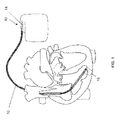
- Fig. 1 shows an electrode lead 10 with a proximal end 12 to which an electrical connector 14 is provided.
- the electrode lead 10 has a distal end 16 with an electrode head 18 formed as a composite component.
- the electrode lead 10 is an elongated electrical lead and has at least one electrical conductor extending from the proximal to the distal end, thus establishing an electrical connection between the electrode head 18 and the electrical terminal 14.
- the electrical conductor is preferably made of titanium.
- the electrode head 18 preferably has a main body made of titanium. The electrode line is thus X-ray transparent.
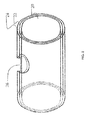
- FIGS 2 and 3 schematically show the structure of the electrode head as a composite component. At least one metal layer 22 is applied to an insulating base body 20. This is on the outside substantially completely covered by a ceramic layer 24, which serves as an insulating layer.
- the electrically insulating main body 20 itself may consist of several components and, for example, preferably consists of a metallic base body on which an inner insulating layer, preferably also a ceramic layer, is applied. Between the in Fig. 2 illustrated base 20 and the metal layer 22 may therefore still be an insulating layer.
- the outer ceramic layer 24 has a defect 26, so that the metal layer 24 in the region of the defect 26 is no longer electrically separated from the environment of the composite component 18 by the outer ceramic layer 24.
- spark erosion can occur, which leads to evaporation of the metal layer 22 in the region of the defect 26, so that, as a result, the remaining metal layer 22 is again galvanically separated from the environment of the composite component 18.
- Fig. 3 shows a composite component similar to the composite component Fig. 2 with the difference being that at the composite component Fig. 3 a plurality of metal layers and a plurality of ceramic layers are applied.
- a defect 26.1 in an insulating layer 24.1 located between two metal layers 22.1 and 22.2 is meaningless because this defect is covered by a second metal layer 22.2 and the outer ceramic layer 24.2.
- the defect 26.2 also shown by way of example, is the same as with the defect 26 from the exemplary embodiment in FIG Fig. 2 , In the area of the defect 26.2, spark erosion occurs and, as a result, the metal layer 22.2 evaporates in the region of the defect 26.2.
- the insulation on head electrodes or sleeves on implantable electrodes can erode due to chemical, electrical and / or mechanical external influences.
- the mechanical strength of the insulation is ensured by the ceramic.
- Occurring defects of the ceramic layer can be remedied by the electrically active metal layers by means of spark erosion.
- the long-term stability is thereby increased.
- the result is an insulating thin film ( ⁇ 10 microns), which is largely resistant to mechanical, chemical and electrical stress and in particular chemically inert and stable to mechanical and electrical influences. This ensures a long-lasting stability of the electrical properties (DC resistance) of the coating and prevents unwanted erosion.
- a 1-2 ⁇ m thick silicon carbide (SiC) is applied to a titanium base by PVD.
- Subsequent vapor deposition with titanium metallizes the SiC layer until a titanium layer ⁇ 500 nm thick, which is a few nanometers thick, is formed.
- Pinholes are filled by the metal and the metal thin layer (metal layer) is electrically connected to the base body made of titanium.
- Sputtering (at least) another SiC layer is applied over the metal layer. Resulting Pinholes are with very little probability on the pinholes of the lower SiC layer. The probability can be further reduced by increasing the number of layers to 3 or more.
- spark erosion is provoked at pinholes of the outer SiC layer and the thin metallization located there is vaporized.
- Outer pinhole and inner head sleeve are electrically separated by this method, whereby a kind of self-healing is achieved.
- a defect 26.2 in the outer ceramic layer 26.2 merely results in the inner metal layer 22.1 penetrating the middle ceramic layer 24.1 and the outer metal layer 22.2 preventing the electrolyte from penetrating protected further departure.
- Advantage of the presented inventive solution is a high strength of a thin insulation of electrodes of less than 10 microns associated with a high manufacturing tolerance. Defects of the ceramic layer that affect the functionality of the electrode can be rectified electrically later.
Landscapes
- Health & Medical Sciences (AREA)
- Engineering & Computer Science (AREA)
- Heart & Thoracic Surgery (AREA)
- Chemical & Material Sciences (AREA)
- Life Sciences & Earth Sciences (AREA)
- Public Health (AREA)
- Nuclear Medicine, Radiotherapy & Molecular Imaging (AREA)
- Radiology & Medical Imaging (AREA)
- Cardiology (AREA)
- Animal Behavior & Ethology (AREA)
- General Health & Medical Sciences (AREA)
- Veterinary Medicine (AREA)
- Biomedical Technology (AREA)
- Inorganic Chemistry (AREA)
- Ceramic Engineering (AREA)
- Vascular Medicine (AREA)
- Electrotherapy Devices (AREA)
- Biophysics (AREA)
- Thermistors And Varistors (AREA)
Abstract
Description
- Die Erfindung betrifft eine langgestreckte, implantierbare elektrische Leitung mit einer Endkomponente an einem Längsende der elektrischen Leitung, wobei die Endkomponente wenigstens eine elektrisch leitfähige, mit der elektrischen Leitung elektrisch verbundene Elektrodenfläche aufweist.
- Solche langgestreckten, implantierbaren elektrischen Leitungen sind beispielsweise als Elektrodenleitungen, wie Stimulationselektrodenleitungen für implantierbare Herzschrittmacher oder Defibrillatoren, bekannt. Solche Elektrodenleitungen haben typischer Weise ein proximales Ende mit einem elektrischen Anschluss zum Anschließen der Elektrodenleitung an ein Stimulationsgerät, wie einen Herzschrittmacher oder Defibrillator, sowie ein distales Ende, an dem typischer Weise Stimulations- oder auch Abführelektroden angeordnet sind. Häufig ist am distalen Ende einer Elektrodenleitung ein Elektrodenkopf angeordnet, der eine sogenannte Tipp-Elektrode bildet. Mit geringem Abstand von der Tipp-Elektrode können auch eine oder mehrere Ringelektroden vorgesehen sein.
- Aus der europäischen Patentanmeldung
EP 0 787 507 ist eine Stimulationselektrodenleitung bekannt, bei der eine metallische Elektrode vollständig mit einer Isolierschicht überzogen ist. Als Metall der Elektrode ist Titan genannt und die Isolierschicht auf der Elektrode ist Titanoxid mit einer Schichtdicke in der Größenordnung von 1 µm. Alternativ ist als Metall der Elektrode Aluminium genannt und als Material der Isolierschicht Aluminiumoxid. - Der Erfindung liegt die Aufgabe zugrunde, eine alternative und möglichst verbesserte langgestreckte elektrische Leitung der eingangs genannten Art zu schaffen. Erfindungsgemäß wird diese Aufgabe dadurch gelöst, dass die Endkomponente eine Verbundkomponente ist, die wenigstens eine dünne Metallschicht mit einer Schichtdicke unter 1 µm aufweist. Die dünne Metallschicht ist dabei auf elektrisch isolierendes Material der Verbundkomponente aufgebracht. Außerdem ist die dünne Metallschicht mit der elektrischen Leitung leitend verbunden und kann daher beispielsweise als Elektrodenfläche dienen. Auf ihrer Außenseite ist die dünne Metallschicht von wenigstens einer äußeren keramischen Schicht nahezu vollständig oder vollständig bedeckt. Im Idealfall ist die dünne Metallschicht dabei vollständig von der äußeren keramischen Schicht bedeckt und durch diese gegenüber der Umgebung elektrisch isoliert. Jedoch haben keramische Schichten neben vielen Vorteilen den Nachteil, dass sie kleine Löcher oder Fehlstellen, sogenannte Pinholes, aufweisen können, die dazu führen können, dass die dünne Metallschicht nicht mehr galvanisch von der Umgebung der Verbundkomponente getrennt ist.
- Der Vorteil einer äußeren keramischen Schicht ist, dass diese auch bei geringer Dicke mechanisch und chemisch stabil ist. Ein Nachteil ist, dass keramische Schichten empfindlich gegenüber elektrischen Effekten, wie Funkenerosion, sind. Insbesondere führen kleine Fehlstellen in der Beschichtung (die Pinholes) bei elektrischer Belastung zur Ausbildung von Plasmakanälen. Diese Plasmakanäle erzeugen bei Entladung Temperaturspitzen, die Beschädigungen sowohl der isolierenden Schicht als auch der Trägerschicht zur Folge haben. Jede Beschädigung dieser Art kann zur Fehlfunktion der Elektrode beim Abfühlen (Sensing) oder Stimulieren (Pacing) führen. Eine bloße Vergrößerung der Schichtdicke der keramischen Schicht erhöht deren Langzeitstabilität nicht, da sich durch Vergrößerung der Schichtdicke Pinholes nicht schließen oder vermeiden lassen.
- Die Erfinder haben diese den grundsätzlichen Vorteilen gegenüberstehenden Nachteile keramischer Isolierschichten erkannt und begegnen diesen dadurch, dass die Metallschicht dünn ausgebildet ist, so dass sie im Falle eines Pinhole infolge der ursprünglich als problematisch erkannten elektrischen Entladung verdampft, also durch Funkenerosion abgetragen wird, so dass die sich nicht im Bereich des Pinhole befindende übrige dünne Metallschicht schließlich wieder vollständig von der Umgebung der Verbundkomponente elektrisch isoliert ist.
- Geeignete Schichtdicken für die äußere keramische Schicht sind vorzugsweise kleiner als 10 µm und vorzugsweise größer als 1 µm. Die Metallschicht hat vorzugsweise eine Schichtdicke kleiner als 100 nm, beispielsweise in der Größenordnung von 10 nm.
- Das elektrisch isolierende Material, auf das die dünne Metallschicht aufgebracht ist, ist vorzugsweise ebenfalls ein keramisches Material. Insbesondere kann das elektrisch isolierende Material eine Isolierschicht sein, die auf einen metallischen Grundkörper aufgetragen ist. Besteht diese Isolierschicht ebenfalls aus keramischem Material - ist sie also ebenfalls eine keramische Schicht -, kann sie zwar ebenso wie die äußere keramische Schicht Pinholes aufweisen, die zur Folge haben können, dass die dünne Metallschicht den metallischen Grundkörper elektrisch kontaktiert. Jedoch ist es äußerst unwahrscheinlich, dass ein Pinhole in der Isolierschicht unter der dünnen Metallschicht sich an gleicher Stelle befindet wie ein Pinhole in der äußeren keramischen Schicht. Damit wäre ein Pinhole in der das elektrisch isolierende Material bildenden Schicht, auf das die Metallschicht aufgebracht ist, unkritisch. Um die Sicherheit noch weiter zu vergrößern, können mehrere Isolierschichten und dünne Metallschichten im Wechsel aufeinander folgen, so dass die Verbundkomponente mehrere dünne Metallschichten und dazwischenliegende Isolierschichten aufweist, wobei diese Isolierschichten vorzugsweise keramische Schichten sind. Die Metallschicht oder die Metallschichten sind dabei vorzugsweise immer dünner als die entsprechenden Keramikschichten.
- Ein geeignetes Material für die keramische Schicht oder die keramischen Schichten sind beispielsweise Siliziumoxid oder Siliziumcarbid, oder auch ein Metalloxid, wie Aluminiumoxid oder Tantaloxid. Die dünne Metallschicht kann beispielsweise eine Titanschicht sein. Ebenso kann das Material eines gegebenenfalls vorhandenen metallischen Grundkörpers Titan sein.
- Die dünne Metallschicht, und im Falle mehrerer dünner Metallschichten insbesondere die äußerste dünne Metallschicht, wirkt dabei als Elektrodenfläche, und die langgestreckte elektrische Leitung ist vorzugsweise eine Stimulationselektrodenleitung, insbesondere für ein implantierbares Stimulationsgerät, wie beispielsweise einen Herzschrittmacher oder Defibrillator.
- Die Verbundkomponente der langgestreckten elektrischen Leitung stellt einen grundsätzlich auch unabhängig von der übrigen langgestreckten elektrischen Leitung herstellbaren Gegenstand dar, der auch als selbständig schutzfähig betrachtet wird.
- Die erfindungsgemäße elektrische Leitung und insbesondere ihre Verbundkomponente wird vorzugsweise mit einem Herstellverfahren erzeugt, bei dem eine oder mehrere keramische Schichten mittels physikalischer Gasabscheidung (PVD, Physical Vapor Deposition) aufgebracht werden. Zusätzlich oder alternativ kann das Herstellverfahren auch den Verfahrensschritt enthalten, dass eine oder mehrere Metallschichten mittels chemischer Gasabscheidung (CVD, Chemical Vapor Deposition) aufgebracht werden.
- Der Schritt der Funkenerosion zum Verdampfen der dünnen Metallschicht im Bereich von Pinholes der äußeren keramischen Schicht kann ebenfalls bereits bei der Herstellung der erfindungsgemäßen elektrischen Leitung bzw. der erfindungsgemäßen Verbundkomponente durchgeführt werden.
- Die erfindungsgemäße Verbundkomponente stellt vorzugsweise einen Elektrodenkopf für eine Stimulationselektrodenleitung dar.
- Die Erfindung soll nun anhand eines Ausführungsbeispiels mit Bezug auf die Figuren näher erläutert werden. Von den Figuren zeigt:
- Fig. 1:
- Eine schematische Ansicht einer Stimulationselektrodenleitung;
- Fig. 2:
- eine schematische Darstellung einer Verbundkomponente mit einem Grundkörper aus elektrisch nicht leitendem Material und einer dünnen Metallschicht sowie einer äußeren keramischen Schicht;
- Fig. 3:
- eine Variante einer Verbundkomponente mit mehreren Metallschichten und mehreren keramischen Schichten.
-
Fig. 1 zeigt eine Elektrodenleitung 10 mit einem proximalen Ende 12, an dem eine elektrische Steckverbindung 14 vorgesehen ist. Die Elektrodenleitung 10 besitzt ein distales Ende 16 mit einem Elektrodenkopf 18, der als Verbundkomponente ausgebildet ist. Die Elektrodenleitung 10 ist eine langgestreckte elektrische Leitung und besitzt wenigstens einen elektrischen Leiter, der sich vom proximalen zum distalen Ende erstreckt und somit eine elektrische Verbindung zwischen dem Elektrodenkopf 18 und dem elektrischen Anschluss 14 herstellt. Der elektrische Leiter besteht vorzugsweise aus Titan. Genauso besitzt der Elektrodenkopf 18 vorzugsweise einen Grundkörper aus Titan. Die Elektrodenleitung ist damit Röntgen-transparent. -
Figuren 2 und3 zeigen schematisch den Aufbau des Elektrodenkopfes als Verbundkomponente. Auf einen isolierenden Grundkörper 20 ist wenigstens eine Metallschicht 22 aufgebracht. Diese ist auf der Außenseite im Wesentlichen vollständig von einer keramischen Schicht 24 bedeckt, die als Isolierschicht dient. - Nicht dargestellt ist, dass der elektrisch isolierende Grundkörper 20 selbst aus mehreren Komponenten bestehen kann und beispielsweise vorzugsweise aus einem metallischen Grundkörper besteht, auf den eine innere Isolierschicht, vorzugsweise ebenfalls eine keramische Schicht, aufgebracht ist. Zwischen dem in
Fig. 2 dargestellten Grundkörper 20 und der Metallschicht 22 kann sich also noch eine Isolierschicht befinden. - Wie in
Fig. 2 beispielshaft dargestellt ist, besitzt die äußere keramische Schicht 24 eine Fehlstelle 26, so dass die Metallschicht 24 im Bereich der Fehlstelle 26 nicht mehr durch die äußere keramische Schicht 24 galvanisch von der Umgebung der Verbundkomponente 18 getrennt ist. Im Bereich der Fehlstelle 26 kann es daher zu einer Funkenerosion kommen, die zum Verdampfen der Metallschicht 22 im Bereich der Fehlstelle 26 führt, so dass im Ergebnis die verbleibende Metallschicht 22 wieder galvanisch von der Umgebung der Verbundkomponente 18 getrennt ist. -
Fig. 3 zeigt eine Verbundkomponente ähnlich der Verbundkomponente ausFig. 2 mit dem Unterschied, dass bei der Verbundkomponente ausFig. 3 mehrere Metallschichten und mehrere keramische Schichten aufgebracht sind. Eine Fehlstelle 26.1 in einer zwischen zwei Metallschichten 22.1 und 22.2 liegenden Isolierschicht 24.1 ist im Ergebnis bedeutungslos, weil diese Fehlstelle von einer zweiten Metallschicht 22.2 und der äußeren keramischen Schicht 24.2 bedeckt ist. Mit der ebenfalls beispielhaft dargestellten Fehlstelle 26.2 verhält es sich hingegen genauso wie mit der Fehlstelle 26 aus dem Ausführungsbeispiel inFig. 2 . Im Bereich der Fehlstelle 26.2 kommt es zur Funkenerosion und infolge dessen zum Verdampfen der Metallschicht 22.2 im Bereich der Fehlstelle 26.2. - Die Isolierung an Kopfelektroden oder -hülsen an implantierbaren Elektroden kann durch chemische, elektrische und/oder mechanische äußere Einwirkungen erodieren. Bei einer Sandwichbauweise von abwechselnd metallischen und keramischen Schichten ist die mechanische Festigkeit der Isolierung durch die Keramik gewährleistet. Auftretende Fehlstellen der keramischen Schicht können durch die elektrisch wirksamen Metallschichten mittels Funkenerosion behoben werden. Die Langzeitstabilität wird dadurch erhöht. Es ergibt sich eine isolierende Dünnschicht (<10 µm), die weitestgehend resistent gegen mechanische, chemische und elektrische Belastung und insbesondere chemisch inert und stabil gegenüber mechanischen und elektrischen Einflüssen ist. Dies sichert eine langandauernde Stabilität der elektrischen Eigenschaften (Gleichstromwiderstand) der Beschichtung und verhindert ungewollte Erosion.
- Zur Herstellung einer röntgendurchsichtigen Titan-Kopfelektrode oder -hülse für einer implantierbare Elektrodenleitung wird auf eine Grundkörper aus Titan durch PVD-Verfahren eine 1-2µm dicke Silizium-Carbid (SiC) aufgebracht. Durch anschließendes Bedampfen mit Titan wird die SiC-Schicht metallisiert bis eine wenige Nanometer dicke Titanschicht < 500nm entsteht. Pinholes werden dabei durch das Metall aufgefüllt und die metallene Dünnschicht (Metallschicht) ist elektrisch mit dem Grundkörper aus Titan verbunden. Über die Metallschicht wird durch Sputtern (mindestens) eine weitere SiC-Schicht aufgetragen. Dabei entstehende Pinholes befinden sich mit nur sehr geringer Wahrscheinlichkeit über den Pinholes der unteren SiC-Schicht. Die Wahrscheinlichkeit kann weiter verringert werden indem die Anzahl der Lagen auf 3 oder mehr erhöht wird. Mit Anlegen einer elektrischen Spannung an den Schichtverbund wird an Pinholes der äußeren SiC-Schicht Funkenerosion provoziert und die dort befindliche dünne Metallisierung verdampft.
- Äußeres Pinhole und innere Kopfhülse sind nach diesem Verfahren elektrisch voneinander getrennt, wodurch eine Art von Selbstheilung erreicht wird.
- Die Vorteile einer mit mehreren Metall- und Isolierschichten versehenen Verbundkomponente ergeben sich aus dem Vergleich der
Figuren 2 und3 . Wird beispielsweise im Lauf der Verwendung der Elektrodenleitung die äußere keramische Schicht 24 durch mechanische, chemische oder elektrische Beanspruchung verletzt (Fehlstelle 26) ist die darunterliegende äußere Metallschicht 22 galvanisch der Umgebung der Verbundkomponente (z.B. ein Elektrolyt wie Blut) verbunden und die Funktion der Elektrode wird beeinträchtigt. - Besitzt die Verbundkomponente mehrere Metallschichten 22.1 und 22.2 und keramische Schichten 24.1 und 24.2 hat eine Fehlstelle 26.2 in der äußern keramischen Schicht 26.2 lediglich zur Folge dass die innere Metallschicht 22.1 durch die mittlere keramische Schicht 24.1 und die äußere Metallschicht 22.2 vor dem Eindringen von Elektrolyt und einem weiteren Aufbruch geschützt.
- Vorteil der vorgestellten erfindungsmäßigen Lösung ist eine hohe Festigkeit einer dünnen Isolierung von Elektroden von unter 10 µm verbunden mit einer hohen Fertigungstoleranz. Fehlstellen der Keramikschicht, die die Funktionalität der Elektrode beeinträchtigen, können nachträglich elektrisch behoben werden.
Claims (15)
- Langgestreckte, implantierbare elektrische Leitung (10) mit einer Endkomponente (18) an einem Längsende der elektrischen Leitung, wobei die Endkomponente (18) wenigstens eine elektrisch leitfähige, mit der elektrischen Leitung elektrisch verbundene Elektrodenfläche aufweist,
dadurch gekennzeichnet dass die Endkomponente (18) eine Verbundkomponente ist, die wenigstes eine dünne Metallschicht (22) mit einer Schichtdicke unter 1µm aufweist, welche- auf elektrisch isolierendes Material aufgebracht ist,- mit der elektrischen Leitung leitend verbunden und- auf ihrer Außenseite von wenigstens einer äußeren isolierenden, vorzugsweise keramischen, Schicht (24) nahezu vollständig oder vollständig bedeckt ist. - Elektrische Leitung (10) gemäß Anspruch 1, dadurch gekennzeichnet, dass die isolierende Schicht (24) keramisch ist und eine Schichtdicke kleiner 10µm hat.
- Elektrische Leitung (10) gemäß Anspruch 1 oder 2, dadurch gekennzeichnet, dass die Schicht (24) keramisch ist und eine Schichtdicke größer 1µm hat.
- Elektrische Leitung gemäß einem der Ansprüche 1 bis 3, dadurch gekennzeichnet, dass die Metallschicht (22) eine Schichtdicke kleiner 100 nm hat
- Elektrische Leitung (10) gemäß einem der Ansprüche 1 bis 4, dadurch gekennzeichnet, dass die Verbundkomponente (18) einen Grundkörper (20) aus Metall besitzt, auf den eine innere Isolierschicht aufgetragen ist, auf welche die dünne Metallschicht (22) aufgetragen ist.
- Elektrische Leitung (10) gemäß einem der Ansprüche 1 bis 5, dadurch gekennzeichnet, dass die dünne Metallschicht die Elektrodenfläche bildet und durch die keramische Schicht von der Umgebung der Verbundkomponente elektrisch isoliert ist.
- Elektrische Leitung (10) gemäß einem der Ansprüche 1 bis 6, dadurch gekennzeichnet, dass die Verbundkomponente (18) mehrere dünne Metallschichten (22.1, 22.1) und dazwischenliegende Isolierschichten (24.1) aufweist.
- Elektrische Leitung (10) gemäß einem der Ansprüche 6 oder 8, dadurch gekennzeichnet, dass die Isolierschicht (24) oder die Isolierschichten (24.1, 24.2) keramische Schichten sind.
- Elektrische Leitung (10) gemäß einem der Ansprüche 1 bis 8, dadurch gekennzeichnet, dass die Metallschicht (22) oder -schichten (22.1, 22.2) dünner sind als die keramische Schicht (24) oder Schichten (24.1, 24.2).
- Elektrische Leitung gemäß einem der Ansprüche 1 bis 9, dadurch gekennzeichnet, dass die keramische Schicht (24) oder die keramischen Schichten (24.1, 24.2) Siliziumoxid, Siliziumcarbid oder ein Metalloxid wie Alumiumoxid oder Tantaloxid enthalten oder aus solchem keramischen Material bestehen.
- Elektrische Leitung (10) gemäß einem der Ansprüche 1 bis 10, dadurch gekennzeichnet, dass die Metallschichten (22) sowie die Isolierschichten (24) und die äußere keramische Schicht (24) zusammen eine Dicke von weniger als 10 µm haben.
- Elektrische Leitung (10) gemäß einem der Ansprüche 1 bis 12, dadurch gekennzeichnet, dass das die elektrische Leitung (10) eine Stimulationselektrodenleitung ist.
- Verfahren zum Herstellen einer elektrischen Leitung gemäß einem der Ansprüche 1 bis 12, dadurch gekennzeichnet, dass eine oder mehrere keramische Schichten (24) mittels physikalischer Gasabscheidung (PVD) aufgebracht werden.
- Verfahren zum Herstellen einer elektrischen Leitung (10) gemäß einem der Ansprüche 1 bis 12, dadurch gekennzeichnet, dass eine oder mehrere Metallschichten (22) mittels chemischer Gasabscheidung (CVD) aufgebracht werden.
- Verfahren zum Herstellen einer elektrischen Leitung (10) gemäß einem der Ansprüche 1 bis 12, dadurch gekennzeichnet, dass durch Anlegen elektrischer Spannung eine Funkenerosion der im Bereich von Fehlstellen der äußeren keramischen Schicht (24) ggf. freiliegenden Metallschicht (22) durchgeführt wird.
Applications Claiming Priority (1)
| Application Number | Priority Date | Filing Date | Title |
|---|---|---|---|
| US201361869767P | 2013-08-26 | 2013-08-26 |
Publications (2)
| Publication Number | Publication Date |
|---|---|
| EP2842598A1 true EP2842598A1 (de) | 2015-03-04 |
| EP2842598B1 EP2842598B1 (de) | 2017-05-03 |
Family
ID=51210985
Family Applications (1)
| Application Number | Title | Priority Date | Filing Date |
|---|---|---|---|
| EP14174639.6A Active EP2842598B1 (de) | 2013-08-26 | 2014-06-27 | Elektrodenleitung oder Elektrodenabschnitt einer Elektrodenleitung |
Country Status (2)
| Country | Link |
|---|---|
| US (1) | US9289602B2 (de) |
| EP (1) | EP2842598B1 (de) |
Families Citing this family (2)
| Publication number | Priority date | Publication date | Assignee | Title |
|---|---|---|---|---|
| EP3067090A1 (de) * | 2015-03-10 | 2016-09-14 | BIOTRONIK SE & Co. KG | Elektrodeneinrichtung für Elektrodiagnose und/oder Elektrothererapie sowie Implantat mit einer Elektrodeneinrichtung |
| KR102906960B1 (ko) * | 2022-02-25 | 2026-01-07 | 주식회사 엔포마레 | 뉴럴프로브 |
Citations (4)
| Publication number | Priority date | Publication date | Assignee | Title |
|---|---|---|---|---|
| EP0787507A1 (de) | 1996-02-02 | 1997-08-06 | Pacesetter AB | Medizinische Vorrichtung zur Gewebestimulierung |
| US20050084672A1 (en) * | 2003-10-20 | 2005-04-21 | O'brien Robert C. | Implantable electrical lead wire |
| EP1574181A1 (de) * | 2002-12-18 | 2005-09-14 | Instituto Cientifico Y Tecnologico De Navarra, S.A. | Elektrodenlagerführung,cochlear-implantat mit der führung und herstellungsverfahren dafür |
| US20080177353A1 (en) * | 2006-12-28 | 2008-07-24 | Takashi Hirota | Cochlear implant device, extracorporeal sound collector, and cochlear implant system having the same |
Family Cites Families (1)
| Publication number | Priority date | Publication date | Assignee | Title |
|---|---|---|---|---|
| DE102009023163B4 (de) * | 2009-05-29 | 2011-12-08 | W.C. Heraeus Gmbh | Stimulationselektrode |
-
2014
- 2014-06-27 EP EP14174639.6A patent/EP2842598B1/de active Active
- 2014-08-19 US US14/463,501 patent/US9289602B2/en active Active
Patent Citations (4)
| Publication number | Priority date | Publication date | Assignee | Title |
|---|---|---|---|---|
| EP0787507A1 (de) | 1996-02-02 | 1997-08-06 | Pacesetter AB | Medizinische Vorrichtung zur Gewebestimulierung |
| EP1574181A1 (de) * | 2002-12-18 | 2005-09-14 | Instituto Cientifico Y Tecnologico De Navarra, S.A. | Elektrodenlagerführung,cochlear-implantat mit der führung und herstellungsverfahren dafür |
| US20050084672A1 (en) * | 2003-10-20 | 2005-04-21 | O'brien Robert C. | Implantable electrical lead wire |
| US20080177353A1 (en) * | 2006-12-28 | 2008-07-24 | Takashi Hirota | Cochlear implant device, extracorporeal sound collector, and cochlear implant system having the same |
Also Published As
| Publication number | Publication date |
|---|---|
| US20150057732A1 (en) | 2015-02-26 |
| US9289602B2 (en) | 2016-03-22 |
| EP2842598B1 (de) | 2017-05-03 |
Similar Documents
| Publication | Publication Date | Title |
|---|---|---|
| EP0116280B1 (de) | Bipolare Elektrode für medizinische Anwendungen | |
| EP0753868B1 (de) | Elektrolytkondensator, insbesondere Tantal-Elektrolytkondensator | |
| DE69114895T2 (de) | Poröse Elektrode mit vergrösserter Reaktionsoberfläche. | |
| EP1430489B1 (de) | Elektrokeramisches bauelement mit mehreren kontaktflächen | |
| DE69724844T2 (de) | Medizinische Vorrichtung zur Gewebestimulierung | |
| DE19641249C2 (de) | Kondensator | |
| DE10307825A1 (de) | Elektrisches Vielschichtbauelement und Schichtstapel | |
| DE2613086B2 (de) | Endocardelektrode | |
| DE4324185A1 (de) | Elektrode für elektromedizinische Anwendungen | |
| EP0944909A1 (de) | Elektro-keramisches bauelement und verfahren zu seiner herstellung | |
| EP2104941B1 (de) | Elektrisches bauelement sowie aussenkontakt eines elektrischen bauelements | |
| EP2842598B1 (de) | Elektrodenleitung oder Elektrodenabschnitt einer Elektrodenleitung | |
| DE102020133165B4 (de) | Keramikelektrode, Baugruppe mit der Keramikelektrode, Anordnung mit der Keramikelektrode und Verfahren zur Herstellung einer Keramikelektrode | |
| EP2191483B1 (de) | Elektrisches vielschichtbauelement | |
| DE2831791C2 (de) | Bauteil aus metallischem Werkstoff mit aufladungsgefährdeter Oberfläche und Verwendung hierfür | |
| EP2054951B1 (de) | Piezoelektrisches bauelement | |
| DE102019106677A1 (de) | Elektrodenelement für einen Energiespeicher, Energiespeicher und Verfahren zur Herstellung eines Elektrodenelements | |
| DE102020118372B3 (de) | Mehrlagige Ringelektrode mit mehreren Öffnungen und Diffusionszwischenschicht | |
| DE4130390C2 (de) | Widerstandselement | |
| DE1764664A1 (de) | Kondensator mit Ionen leitendem keramischem Elektrolyt | |
| WO2020104258A1 (de) | Multipolare kanüle | |
| DE102016107414A1 (de) | Durchführung eines implantierbaren medizinelektronischen Gerätes und implantierbares medizinelektronisches Gerät | |
| DE19812873B4 (de) | Elektrolytkondensator | |
| WO2014001006A1 (de) | Verfahren zum ausbilden einer elektrisch leitenden struktur an einem trägerelement, schichtanordnung sowie verwendung eines verfahrens oder einer schichtanordnung | |
| DE102013210117A1 (de) | Gasentladungsröhre mit Zündhilfe |
Legal Events
| Date | Code | Title | Description |
|---|---|---|---|
| 17P | Request for examination filed |
Effective date: 20140627 |
|
| AK | Designated contracting states |
Kind code of ref document: A1 Designated state(s): AL AT BE BG CH CY CZ DE DK EE ES FI FR GB GR HR HU IE IS IT LI LT LU LV MC MK MT NL NO PL PT RO RS SE SI SK SM TR |
|
| AX | Request for extension of the european patent |
Extension state: BA ME |
|
| PUAI | Public reference made under article 153(3) epc to a published international application that has entered the european phase |
Free format text: ORIGINAL CODE: 0009012 |
|
| R17P | Request for examination filed (corrected) |
Effective date: 20150616 |
|
| RBV | Designated contracting states (corrected) |
Designated state(s): AL AT BE BG CH CY CZ DE DK EE ES FI FR GB GR HR HU IE IS IT LI LT LU LV MC MK MT NL NO PL PT RO RS SE SI SK SM TR |
|
| RIC1 | Information provided on ipc code assigned before grant |
Ipc: A61N 1/05 20060101AFI20161026BHEP |
|
| GRAP | Despatch of communication of intention to grant a patent |
Free format text: ORIGINAL CODE: EPIDOSNIGR1 |
|
| INTG | Intention to grant announced |
Effective date: 20161208 |
|
| GRAS | Grant fee paid |
Free format text: ORIGINAL CODE: EPIDOSNIGR3 |
|
| GRAA | (expected) grant |
Free format text: ORIGINAL CODE: 0009210 |
|
| AK | Designated contracting states |
Kind code of ref document: B1 Designated state(s): AL AT BE BG CH CY CZ DE DK EE ES FI FR GB GR HR HU IE IS IT LI LT LU LV MC MK MT NL NO PL PT RO RS SE SI SK SM TR |
|
| REG | Reference to a national code |
Ref country code: GB Ref legal event code: FG4D Free format text: NOT ENGLISH |
|
| REG | Reference to a national code |
Ref country code: AT Ref legal event code: REF Ref document number: 889299 Country of ref document: AT Kind code of ref document: T Effective date: 20170515 Ref country code: CH Ref legal event code: EP |
|
| REG | Reference to a national code |
Ref country code: IE Ref legal event code: FG4D Free format text: LANGUAGE OF EP DOCUMENT: GERMAN |
|
| REG | Reference to a national code |
Ref country code: DE Ref legal event code: R096 Ref document number: 502014003615 Country of ref document: DE |
|
| REG | Reference to a national code |
Ref country code: NL Ref legal event code: MP Effective date: 20170503 |
|
| REG | Reference to a national code |
Ref country code: LT Ref legal event code: MG4D |
|
| PG25 | Lapsed in a contracting state [announced via postgrant information from national office to epo] |
Ref country code: NO Free format text: LAPSE BECAUSE OF FAILURE TO SUBMIT A TRANSLATION OF THE DESCRIPTION OR TO PAY THE FEE WITHIN THE PRESCRIBED TIME-LIMIT Effective date: 20170803 Ref country code: FI Free format text: LAPSE BECAUSE OF FAILURE TO SUBMIT A TRANSLATION OF THE DESCRIPTION OR TO PAY THE FEE WITHIN THE PRESCRIBED TIME-LIMIT Effective date: 20170503 Ref country code: LT Free format text: LAPSE BECAUSE OF FAILURE TO SUBMIT A TRANSLATION OF THE DESCRIPTION OR TO PAY THE FEE WITHIN THE PRESCRIBED TIME-LIMIT Effective date: 20170503 Ref country code: HR Free format text: LAPSE BECAUSE OF FAILURE TO SUBMIT A TRANSLATION OF THE DESCRIPTION OR TO PAY THE FEE WITHIN THE PRESCRIBED TIME-LIMIT Effective date: 20170503 Ref country code: ES Free format text: LAPSE BECAUSE OF FAILURE TO SUBMIT A TRANSLATION OF THE DESCRIPTION OR TO PAY THE FEE WITHIN THE PRESCRIBED TIME-LIMIT Effective date: 20170503 Ref country code: GR Free format text: LAPSE BECAUSE OF FAILURE TO SUBMIT A TRANSLATION OF THE DESCRIPTION OR TO PAY THE FEE WITHIN THE PRESCRIBED TIME-LIMIT Effective date: 20170804 |
|
| PG25 | Lapsed in a contracting state [announced via postgrant information from national office to epo] |
Ref country code: RS Free format text: LAPSE BECAUSE OF FAILURE TO SUBMIT A TRANSLATION OF THE DESCRIPTION OR TO PAY THE FEE WITHIN THE PRESCRIBED TIME-LIMIT Effective date: 20170503 Ref country code: IS Free format text: LAPSE BECAUSE OF FAILURE TO SUBMIT A TRANSLATION OF THE DESCRIPTION OR TO PAY THE FEE WITHIN THE PRESCRIBED TIME-LIMIT Effective date: 20170903 Ref country code: PL Free format text: LAPSE BECAUSE OF FAILURE TO SUBMIT A TRANSLATION OF THE DESCRIPTION OR TO PAY THE FEE WITHIN THE PRESCRIBED TIME-LIMIT Effective date: 20170503 Ref country code: SE Free format text: LAPSE BECAUSE OF FAILURE TO SUBMIT A TRANSLATION OF THE DESCRIPTION OR TO PAY THE FEE WITHIN THE PRESCRIBED TIME-LIMIT Effective date: 20170503 Ref country code: BG Free format text: LAPSE BECAUSE OF FAILURE TO SUBMIT A TRANSLATION OF THE DESCRIPTION OR TO PAY THE FEE WITHIN THE PRESCRIBED TIME-LIMIT Effective date: 20170803 Ref country code: LV Free format text: LAPSE BECAUSE OF FAILURE TO SUBMIT A TRANSLATION OF THE DESCRIPTION OR TO PAY THE FEE WITHIN THE PRESCRIBED TIME-LIMIT Effective date: 20170503 Ref country code: NL Free format text: LAPSE BECAUSE OF FAILURE TO SUBMIT A TRANSLATION OF THE DESCRIPTION OR TO PAY THE FEE WITHIN THE PRESCRIBED TIME-LIMIT Effective date: 20170503 |
|
| PG25 | Lapsed in a contracting state [announced via postgrant information from national office to epo] |
Ref country code: EE Free format text: LAPSE BECAUSE OF FAILURE TO SUBMIT A TRANSLATION OF THE DESCRIPTION OR TO PAY THE FEE WITHIN THE PRESCRIBED TIME-LIMIT Effective date: 20170503 Ref country code: RO Free format text: LAPSE BECAUSE OF FAILURE TO SUBMIT A TRANSLATION OF THE DESCRIPTION OR TO PAY THE FEE WITHIN THE PRESCRIBED TIME-LIMIT Effective date: 20170503 Ref country code: DK Free format text: LAPSE BECAUSE OF FAILURE TO SUBMIT A TRANSLATION OF THE DESCRIPTION OR TO PAY THE FEE WITHIN THE PRESCRIBED TIME-LIMIT Effective date: 20170503 Ref country code: SK Free format text: LAPSE BECAUSE OF FAILURE TO SUBMIT A TRANSLATION OF THE DESCRIPTION OR TO PAY THE FEE WITHIN THE PRESCRIBED TIME-LIMIT Effective date: 20170503 Ref country code: CZ Free format text: LAPSE BECAUSE OF FAILURE TO SUBMIT A TRANSLATION OF THE DESCRIPTION OR TO PAY THE FEE WITHIN THE PRESCRIBED TIME-LIMIT Effective date: 20170503 |
|
| REG | Reference to a national code |
Ref country code: DE Ref legal event code: R097 Ref document number: 502014003615 Country of ref document: DE |
|
| PG25 | Lapsed in a contracting state [announced via postgrant information from national office to epo] |
Ref country code: IT Free format text: LAPSE BECAUSE OF FAILURE TO SUBMIT A TRANSLATION OF THE DESCRIPTION OR TO PAY THE FEE WITHIN THE PRESCRIBED TIME-LIMIT Effective date: 20170503 Ref country code: SM Free format text: LAPSE BECAUSE OF FAILURE TO SUBMIT A TRANSLATION OF THE DESCRIPTION OR TO PAY THE FEE WITHIN THE PRESCRIBED TIME-LIMIT Effective date: 20170503 |
|
| PLBE | No opposition filed within time limit |
Free format text: ORIGINAL CODE: 0009261 |
|
| STAA | Information on the status of an ep patent application or granted ep patent |
Free format text: STATUS: NO OPPOSITION FILED WITHIN TIME LIMIT |
|
| REG | Reference to a national code |
Ref country code: FR Ref legal event code: ST Effective date: 20180228 |
|
| 26N | No opposition filed |
Effective date: 20180206 |
|
| PG25 | Lapsed in a contracting state [announced via postgrant information from national office to epo] |
Ref country code: LU Free format text: LAPSE BECAUSE OF NON-PAYMENT OF DUE FEES Effective date: 20170627 |
|
| PG25 | Lapsed in a contracting state [announced via postgrant information from national office to epo] |
Ref country code: SI Free format text: LAPSE BECAUSE OF FAILURE TO SUBMIT A TRANSLATION OF THE DESCRIPTION OR TO PAY THE FEE WITHIN THE PRESCRIBED TIME-LIMIT Effective date: 20170503 Ref country code: FR Free format text: LAPSE BECAUSE OF NON-PAYMENT OF DUE FEES Effective date: 20170703 |
|
| REG | Reference to a national code |
Ref country code: BE Ref legal event code: MM Effective date: 20170630 |
|
| PG25 | Lapsed in a contracting state [announced via postgrant information from national office to epo] |
Ref country code: BE Free format text: LAPSE BECAUSE OF NON-PAYMENT OF DUE FEES Effective date: 20170630 |
|
| PG25 | Lapsed in a contracting state [announced via postgrant information from national office to epo] |
Ref country code: MT Free format text: LAPSE BECAUSE OF FAILURE TO SUBMIT A TRANSLATION OF THE DESCRIPTION OR TO PAY THE FEE WITHIN THE PRESCRIBED TIME-LIMIT Effective date: 20170503 |
|
| GBPC | Gb: european patent ceased through non-payment of renewal fee |
Effective date: 20180627 |
|
| PG25 | Lapsed in a contracting state [announced via postgrant information from national office to epo] |
Ref country code: GB Free format text: LAPSE BECAUSE OF NON-PAYMENT OF DUE FEES Effective date: 20180627 |
|
| PG25 | Lapsed in a contracting state [announced via postgrant information from national office to epo] |
Ref country code: MC Free format text: LAPSE BECAUSE OF FAILURE TO SUBMIT A TRANSLATION OF THE DESCRIPTION OR TO PAY THE FEE WITHIN THE PRESCRIBED TIME-LIMIT Effective date: 20170503 Ref country code: HU Free format text: LAPSE BECAUSE OF FAILURE TO SUBMIT A TRANSLATION OF THE DESCRIPTION OR TO PAY THE FEE WITHIN THE PRESCRIBED TIME-LIMIT; INVALID AB INITIO Effective date: 20140627 |
|
| PG25 | Lapsed in a contracting state [announced via postgrant information from national office to epo] |
Ref country code: CY Free format text: LAPSE BECAUSE OF FAILURE TO SUBMIT A TRANSLATION OF THE DESCRIPTION OR TO PAY THE FEE WITHIN THE PRESCRIBED TIME-LIMIT Effective date: 20170503 |
|
| PG25 | Lapsed in a contracting state [announced via postgrant information from national office to epo] |
Ref country code: MK Free format text: LAPSE BECAUSE OF FAILURE TO SUBMIT A TRANSLATION OF THE DESCRIPTION OR TO PAY THE FEE WITHIN THE PRESCRIBED TIME-LIMIT Effective date: 20170503 |
|
| PG25 | Lapsed in a contracting state [announced via postgrant information from national office to epo] |
Ref country code: TR Free format text: LAPSE BECAUSE OF FAILURE TO SUBMIT A TRANSLATION OF THE DESCRIPTION OR TO PAY THE FEE WITHIN THE PRESCRIBED TIME-LIMIT Effective date: 20170503 |
|
| PG25 | Lapsed in a contracting state [announced via postgrant information from national office to epo] |
Ref country code: PT Free format text: LAPSE BECAUSE OF FAILURE TO SUBMIT A TRANSLATION OF THE DESCRIPTION OR TO PAY THE FEE WITHIN THE PRESCRIBED TIME-LIMIT Effective date: 20170503 |
|
| PG25 | Lapsed in a contracting state [announced via postgrant information from national office to epo] |
Ref country code: AL Free format text: LAPSE BECAUSE OF FAILURE TO SUBMIT A TRANSLATION OF THE DESCRIPTION OR TO PAY THE FEE WITHIN THE PRESCRIBED TIME-LIMIT Effective date: 20170503 |
|
| REG | Reference to a national code |
Ref country code: AT Ref legal event code: MM01 Ref document number: 889299 Country of ref document: AT Kind code of ref document: T Effective date: 20190627 |
|
| PG25 | Lapsed in a contracting state [announced via postgrant information from national office to epo] |
Ref country code: AT Free format text: LAPSE BECAUSE OF NON-PAYMENT OF DUE FEES Effective date: 20190627 |
|
| P01 | Opt-out of the competence of the unified patent court (upc) registered |
Effective date: 20230609 |
|
| PGFP | Annual fee paid to national office [announced via postgrant information from national office to epo] |
Ref country code: IE Payment date: 20240617 Year of fee payment: 11 |
|
| PGFP | Annual fee paid to national office [announced via postgrant information from national office to epo] |
Ref country code: DE Payment date: 20240617 Year of fee payment: 11 |
|
| PGFP | Annual fee paid to national office [announced via postgrant information from national office to epo] |
Ref country code: CH Payment date: 20240701 Year of fee payment: 11 |
|
| REG | Reference to a national code |
Ref country code: DE Ref legal event code: R119 Ref document number: 502014003615 Country of ref document: DE |
|
| REG | Reference to a national code |
Ref country code: CH Ref legal event code: H13 Free format text: ST27 STATUS EVENT CODE: U-0-0-H10-H13 (AS PROVIDED BY THE NATIONAL OFFICE) Effective date: 20260127 |
|
| PG25 | Lapsed in a contracting state [announced via postgrant information from national office to epo] |
Ref country code: DE Free format text: LAPSE BECAUSE OF NON-PAYMENT OF DUE FEES Effective date: 20260101 Ref country code: IE Free format text: LAPSE BECAUSE OF NON-PAYMENT OF DUE FEES Effective date: 20250627 |
|
| PG25 | Lapsed in a contracting state [announced via postgrant information from national office to epo] |
Ref country code: CH Free format text: LAPSE BECAUSE OF NON-PAYMENT OF DUE FEES Effective date: 20250630 |