EP2840407B1 - Accurate current sensing in h-bridge applications without amplifier having high common mode rejection ratio - Google Patents
Accurate current sensing in h-bridge applications without amplifier having high common mode rejection ratio Download PDFInfo
- Publication number
- EP2840407B1 EP2840407B1 EP14002828.3A EP14002828A EP2840407B1 EP 2840407 B1 EP2840407 B1 EP 2840407B1 EP 14002828 A EP14002828 A EP 14002828A EP 2840407 B1 EP2840407 B1 EP 2840407B1
- Authority
- EP
- European Patent Office
- Prior art keywords
- differential amplifier
- voltage
- current sensing
- shunt resistance
- circuit
- Prior art date
- Legal status (The legal status is an assumption and is not a legal conclusion. Google has not performed a legal analysis and makes no representation as to the accuracy of the status listed.)
- Active
Links
Images


Classifications
-
- H—ELECTRICITY
- H02—GENERATION; CONVERSION OR DISTRIBUTION OF ELECTRIC POWER
- H02M—APPARATUS FOR CONVERSION BETWEEN AC AND AC, BETWEEN AC AND DC, OR BETWEEN DC AND DC, AND FOR USE WITH MAINS OR SIMILAR POWER SUPPLY SYSTEMS; CONVERSION OF DC OR AC INPUT POWER INTO SURGE OUTPUT POWER; CONTROL OR REGULATION THEREOF
- H02M3/00—Conversion of DC power input into DC power output
- H02M3/02—Conversion of DC power input into DC power output without intermediate conversion into AC
- H02M3/04—Conversion of DC power input into DC power output without intermediate conversion into AC by static converters
- H02M3/10—Conversion of DC power input into DC power output without intermediate conversion into AC by static converters using discharge tubes with control electrode or semiconductor devices with control electrode
- H02M3/145—Conversion of DC power input into DC power output without intermediate conversion into AC by static converters using discharge tubes with control electrode or semiconductor devices with control electrode using devices of a triode or transistor type requiring continuous application of a control signal
- H02M3/155—Conversion of DC power input into DC power output without intermediate conversion into AC by static converters using discharge tubes with control electrode or semiconductor devices with control electrode using devices of a triode or transistor type requiring continuous application of a control signal using semiconductor devices only
- H02M3/156—Conversion of DC power input into DC power output without intermediate conversion into AC by static converters using discharge tubes with control electrode or semiconductor devices with control electrode using devices of a triode or transistor type requiring continuous application of a control signal using semiconductor devices only with automatic control of output voltage or current, e.g. switching regulators
- H02M3/158—Conversion of DC power input into DC power output without intermediate conversion into AC by static converters using discharge tubes with control electrode or semiconductor devices with control electrode using devices of a triode or transistor type requiring continuous application of a control signal using semiconductor devices only with automatic control of output voltage or current, e.g. switching regulators including plural semiconductor devices as final control devices for a single load
-
- G—PHYSICS
- G01—MEASURING; TESTING
- G01R—MEASURING ELECTRIC VARIABLES; MEASURING MAGNETIC VARIABLES
- G01R19/00—Arrangements for measuring currents or voltages or for indicating presence or sign thereof
- G01R19/0092—Measuring current only
-
- H—ELECTRICITY
- H02—GENERATION; CONVERSION OR DISTRIBUTION OF ELECTRIC POWER
- H02P—CONTROL OR REGULATION OF ELECTRIC MOTORS, ELECTRIC GENERATORS OR DYNAMO-ELECTRIC CONVERTERS; CONTROLLING TRANSFORMERS, REACTORS OR CHOKE COILS
- H02P31/00—Arrangements for regulating or controlling electric motors not provided for in groups H02P1/00 - H02P5/00, H02P7/00 or H02P21/00 - H02P29/00
-
- G—PHYSICS
- G01—MEASURING; TESTING
- G01R—MEASURING ELECTRIC VARIABLES; MEASURING MAGNETIC VARIABLES
- G01R1/00—Details of instruments or arrangements of the types included in groups G01R5/00 - G01R13/00 and G01R31/00
- G01R1/20—Modifications of basic electric elements for use in electric measuring instruments; Structural combinations of such elements with such instruments
- G01R1/203—Resistors used for electric measuring, e.g. decade resistors standards, resistors for comparators, series resistors, shunts
-
- G—PHYSICS
- G01—MEASURING; TESTING
- G01R—MEASURING ELECTRIC VARIABLES; MEASURING MAGNETIC VARIABLES
- G01R19/00—Arrangements for measuring currents or voltages or for indicating presence or sign thereof
- G01R19/165—Indicating that current or voltage is either above or below a predetermined value or within or outside a predetermined range of values
- G01R19/16533—Indicating that current or voltage is either above or below a predetermined value or within or outside a predetermined range of values characterised by the application
- G01R19/16538—Indicating that current or voltage is either above or below a predetermined value or within or outside a predetermined range of values characterised by the application in AC or DC supplies
-
- G—PHYSICS
- G01—MEASURING; TESTING
- G01R—MEASURING ELECTRIC VARIABLES; MEASURING MAGNETIC VARIABLES
- G01R31/00—Arrangements for testing electric properties; Arrangements for locating electric faults; Arrangements for electrical testing characterised by what is being tested not provided for elsewhere
- G01R31/40—Testing power supplies
Definitions
- This disclosure relates to current sensing circuits, including current sensing circuits that control motors driven by an H-bridge of electronic switches.
- the windings of a motor may each be driven by an H-bridge of electronic switches, which may be driven by a pulse-width-modulated (PWM) signal.
- PWM pulse-width-modulated
- the system may need to continually measure the current flowing into (or out of) each motor winding.
- a shunt resistance may be placed in series with each winding, and the differential voltage across each shunt resistance may be measured and serve as an indication of the current that is traveling through it.
- a differential amplifier may be used to measure the differential voltage across the shunt resistance.
- the differential voltage across the shunt resistance may be very low, while the common mode voltage of the shunt resistance -- the instantaneous average of the voltages of the shunt resistance terminals with respect to ground -- may vary widely as the H-bridge is switched by the PWM signal. This may cause errors in the measurements made by the differential amplifier.
- the differential amplifier may have a high common mode voltage rejection ratio (CMRR). This may enable the differential amplifier to accurately track the differential voltage across the shunt resistance, even in the face of wide variations in the common mode voltage.
- CMRR common mode voltage rejection ratio
- AC CMRR AC performance
- Some H-bridge driven motor controllers may not directly measure the current in the motor winding. Instead, they may measure the current in either a ground or a supply connection to switches that form the H-bridge. However, the information provided by this approach may not be as accurate as directly measuring the current to the motor winding.
- US 5 920 189 A discloses a current monitor for measuring current over a wide dynamic range.
- the current monitor includes a low current channel, a high current channel, and a switch for selecting the low current channel if the measured current is below a predetermined level and the high current channel if the current is above the predetermined level.
- the output of the high current channel is voltage encoded by adding a fixed offset.
- the current monitor determines that the measured current is from the low current channel if the reading is below the offset and from the high current channel if the reading is above the offset.
- a current level output device automatically outputs a decoded current reading based on this determination.
- the current monitor also incorporates a low current error compensation circuit to compensate for parasitic current when the current monitor is using the high current channel.
- the current monitor also incorporates a device for reducing the common mode error voltage to zero in the differential amplifiers used to convert current across shunt resistors in the low and high current channels to a voltage signal.
- the problem relates to how to improve the accuracy for current measuring.
- a current sensing circuit may include a shunt resistance through which current to be sensed travels.
- a first and a second differential amplifier may each provide an amplified output of the voltage across the shunt resistance.
- a switching system may deliver a current sensing signal output based on the amplified output of the first differential amplifier when the common mode voltage across the shunt resistance is low and based on the amplified output of the second differential amplifier when the common mode voltage across the shunt resistance is high.
- the first differential amplifier may provide its lowest output DC offset voltage when the common mode voltage is low, while the second differential amplifier may provide its lowest output DC offset voltage when the common mode voltage is high.
- the current sensing circuit may sense current that is controlled by one or more switches that switch at a switching frequency.
- the first and second differential amplifiers may both have a low common mode voltage rejection ratio at the switching frequency, such as a ratio of less than 40dB .
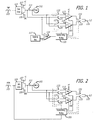
- FIG. 1 is an example of a motor 101 and a circuit for driving a winding of the motor 101 that may include a pulse-width-modulated (PWM) drive signal 103, a gate drive circuit 105, H-bridge switches 107 and 109, and a current sensing circuit.
- the current sensing circuit accurately measures current to the motor 101 and may include a shunt resistance 111, differential amplifiers 113 and 115, and a switching system that includes a threshold bias circuit 117, a comparator 119, a switch timing/nulling circuit 121, and electronic switches 123, 125, 127, 129, 131, and 133.
- the motor 101 may be of any type.
- the motor may be a DC motor whose torque is proportional to input current.
- the motor 101 may have several windings. Each winding may be driven by an additional instance of the circuit illustrated in FIG. 1 .
- the H-bridge switches 107 and 109 may be electronic switches, such as MOSFETs that may be driven at a switching frequency.
- the gate drive circuit 105 may be configured to actuate the H-bridge switches 107 and 109 so as to cause the winding of the motor 101 to be alternatingly connected to a high and a low voltage, such as to a positive supply voltage +V and to ground, in synchronism with state changes of the PWM drive signal 103.
- the gate drive circuit 105 may be configured to cause the winding of the motor 101 to be connected to +V when the PWM drive signal 103 is high and to ground when the PWM drive signal 103 is low.
- the PWM drive signal 103 may be generated by a drive circuit (not shown) that causes the PWM drive signal 103 to have a frequency and/or duty cycle that causes the motor 101 to operate in a particular desired way, such as at a particular position, speed, and/or acceleration. To facilitate this, information about the current that is traveling through the motor 101 may be needed by the drive circuit that generates the PWM drive signal 103. This current information may be obtained by measuring the voltage across the shunt resistance 111.
- the shunt resistance 111 may be a single resistor, a set of resistors, and/or one or more other types of components that have a resistance. The value of the resistance may be low, so as not to cause a large voltage drop and hence energy loss.
- the average of the voltage at the input of the shunt resistance 111 and the voltage at the output of the shunt resistance 111 is known as the common mode voltage.
- This common mode voltage may be very low when the motor winding is connected to ground through the H-bridge switch 109, while it may be very high when the motor winding is connected to +V through the H-bridge switch 107.
- Both differential amplifiers 113 and 115 may be configured to provide an amplified output of the voltage across the shunt resistance 111 when connected across the shunt resistance 111.
- the differential amplifier 113 may be optimized to provide its lowest output DC offset voltage when the common mode voltage is low (e.g., ground).
- the differential amplifier 115 may be optimized to provide its lowest output DC offset voltage when the common mode voltage is high (e.g., +V).
- both of the differential amplifiers 113 and 115 may have a small common mode rejection ratio, such as a ratio that is less than 40dB at the switching frequency.
- the switching system may be configured to cause a current sensing signal output 135 to be based on the amplified output of the first differential amplifier 113 and not the amplified output of the second differential amplifier 115 when the common mode voltage across the shunt resistance 111 is low (e.g., ground). Conversely, the switching system may be configured to cause the current sensing signal output 135 to be based on the amplified output of the second differential amplifier 115 and not the amplified output of the first differential amplifier 113 when the common mode voltage across the shunt resistance 111 is high (e.g., +V).
- Amplifiers 113 and 115 may each have connections to +V and GND, unlike as is illustrated in FIG. 1 . In that case, either may be used as the high common mode amplifier or the low common mode amplifier interchangeably.
- One amplifier might instead be connected to a low voltage, such as 5V and ground, while the other might instead be connected to +V and a voltage near +V, such as (+V - 5V).
- the amplifier tied to +V may serve as the high common mode voltage amplifier, while the one tied to ground may serve as the low common mode amplifier.
- the amplifier 113 When connected as shown in FIG. 1 , the amplifier 113 may be active when the common mode voltage is high, while the amplifier 115 may be active when the common mode voltage is low.
- the switching system may employ any means to facilitate this functionality.
- the threshold bias circuit 117 may generate a reference voltage and the comparator 119 may compare that reference voltage with a voltage on the shunt resistance 111, such as the voltage at the input to the shunt resistance 111.
- the output of the comparator 119 may cause the switch timing/nulling circuit 121 to cause the voltage across the shunt resistance 111 to be amplified by only the differential amplifier 113 by causing switches 123, 125, and 131 to close, while causing switches 127, 129, and 133 to open.
- the output of the comparator 119 may cause the switch timing/nulling circuit 121 to cause the voltage across the shunt resistance 111 to be amplified by only the differential amplifier 115 by causing switches 123, 125, and 131 to open, while causing switches 127, 129, and 133 to close.
- the switches 123, 125, 127, 129, 131, and 133 may be any type of electronic switches, such as MOSFETs.
- each may amplify the differential voltage across the shunt resistance 111 only when the differential amplifier is best matched to the common mode voltage of the shunt resistance 111, i.e., at a time when the common mode voltage is low (e.g., ground) for the differential amplifier 113 that is optimized for low common mode voltages, and at a time when the common mode voltage is high (e.g., +V) for the differential amplifier 115 that is optimized for high common mode voltages.
- the switch timing/nulling circuit 121 may automatically adjust the differential amplifiers 113 and 115 so as to cause their outputs to be zero when there is no differential voltage at their inputs.
- the switch timing/nulling circuit 121 may be configured to perform this function repeatedly during the course of the operation of the current sensing circuit, thereby compensating for drift in this zero output caused by temperature changes, component aging, and/or other reasons.
- the switch timing/nulling circuit 121 may implement any approach for effectuating this auto zeroing function.
- the switch timing/nulling circuit 121 may be configured to zero each of the differential amplifiers 113 and 115 when they are not being used to measure the voltage across the shunt resistance 111, e.g., when the input to the differential amplifier that is being nulled is disconnected from the shunt resistance 111 by opening the switches that connect the differential amplifier to the shunt resistance 111, thereby causing the voltage at the input of the differential amplifier to be zero.
- the switch timing/nulling circuit 121 may then examine the output of the disconnected differential amplifier and provide a compensating input to the differential amplifier that causes its output to also be at zero.
- Example of such nulling approaches may be found in U.S. patent 4,633,642 and European patent 1,428,314 . All or any portion of the switch timing/nulling circuit 121 could be part of the amplifiers 113 and/or 115.
- a clock that runs at a multiple of the frequency of the PWM drive signal 103 may be used to provide non-overlapping clocks.
- a PLL/frequency synthesizer or other type of circuit that can produce a multiple (e.g., doubling or quadrupling) of this frequency from the PWM drive signal 103 or from another signal may be used.
- the switch timing/nulling circuit 121 may instead be configured to null each of the differential amplifiers 113 and 115 while they are measuring the voltage across the shunt resistance 111. Examples of nulling approaches that may be used may be found in U.S. patent 7,292,095 ; " 140dB-CMMR Current-Feedback Instrumentation Amplifier Employing Ping-Pong Auto-Zeroing and Chopping," a paper presented at the 2009 IEEE International Solid-State Circuits Conference ; and " A Micro Power Chopper-Stabilized Operational Amplifier Using A SC Notch Filter With Synchronous Integration Inside The Continuous-Time Signal Path," IEEE Journal of Solid-State Circuits, Vol. 41, No. 12, Dec. 2006 .
- FIG. 2 is an example of the motor 101 and a circuit for driving a winding of the motor that includes a current sense circuit that is similar to the one in FIG. 1 , but that senses the common mode voltage indirectly, as compared to directly. Except as now described, the components in the circuit illustrated in FIG. 2 may be the same as those in FIG. 1 , as described above.
- the circuit in FIG. 2 may have a switch timing/nulling circuit 201 that senses the common mode voltage indirectly, as compared to directly. More specifically, the switch timing/nulling circuit 201 may utilize the PWM drive signal 103 to determine whether the common mode voltage across the shunt resistance 111 is high (e.g., +V) or low (e.g., ground). For example, it may deem each rising edge in the PWM drive signal 103 as indicating a change to a high common mode voltage (e.g., +V), while it may deem each falling edge in the PWM drive signal 103 as indicating a change to a low common mode voltage (e.g., ground). Except for this difference, the switch timing/nulling circuit 201 may be the same as the switch timing/nulling circuit 121 illustrated in FIG. 1 and discussed above.
- the switch timing/nulling circuit 201 may be the same as the switch timing/nulling circuit 121 illustrated in FIG. 1 and discussed above.
- FIG. 3 is an example of the motor 101 and a circuit for driving a winding of the motor that includes a current sense circuit that senses the common mode voltage both directly as in FIG. 1 and indirectly as in FIG. 2 . Except as now described, the components in the circuit illustrated in FIG. 3 may be the same as those in FIG. 1 , as described above.
- the circuit in FIG. 3 may have a switch timing/nulling circuit 301 that senses whether the common mode voltage is high (e.g., +V) or low (e.g., ground) based on both the output of the comparator 119 (a direct measurement) and the PWM drive signal 103 (an indirect measurement).
- the common mode voltage e.g., +V
- the PWM drive signal 103 an indirect measurement
- the switch timing/nulling circuit 301 may switch in the differential amplifier 113 so that it can begin measuring the voltage across the shunt resistance 111 when the voltage on the shunt resistance 111 drops below the voltage produced by the threshold bias circuit 117; may switch out the differential amplifier 113 so that it stops measuring the voltage across the shunt resistance 111 when there is an upward transition in the PWM drive signal 103; may switch in the differential amplifier 115 so that it begins measuring the voltage across the shunt resistance 111 when the voltage on the shunt resistance 111 rises above the voltage produced by the threshold bias circuit 117; and may switch out the differential amplifier 115 so that it stops measuring the voltage across the shunt resistance 111 when there is a downward transition in the PWM drive signal 103. Except for this difference, the switch timing/nulling circuit 301 may be the same as the switch timing/nulling circuit 121 illustrated in FIG. 1 and discussed above.
- FIG. 4 is an example of the motor 101 and a circuit for driving a winding of the motor 101 that includes a current sense circuit that is similar to the one in FIG. 1 , but that uses two comparators to sense whether the common mode voltage is high or low, as compared to a single comparator. Except as now described, the components in the circuit illustrated in FIG. 4 may be the same as those in FIG. 1 , as described above.
- a threshold bias circuit 403 may generate both a high reference voltage 405 and a low reference voltage 407.
- the high reference voltage 405 may be compared by a comparator 409 with the voltage on the shunt resistance 111.
- the low reference voltage 407 may be compared by a comparator 411 with a voltage on the shunt resistance 111.
- a switch timing/nulling circuit 401 may be configured to control the switches 123, 125, 127, 129, 131, and 133 in the same manner as the switch timing/nulling circuit 121.
- the switch timing/nulling circuit 401 may be configured not to switch in the differential amplifier 113 until the voltage on the shunt resistance 111 drops below the low reference voltage 407, as signaled by the comparator 411. Similarly, the switch timing/nulling circuit 401 may be configured not to switch in the differential amplifier 115 until the voltage on the shunt resistance 111 rises above the high reference voltage 405, as signaled by the comparator 409. The switch timing/nulling circuit 401 may be configured to disconnect both differential amplifiers 113 and 115 during a brief period of time when the voltage on the shunt resistance 111 transitions between the low reference voltage 407 and the high reference voltage 405, as signaled by comparators 409 and 411. Except for this difference, the switch timing/nulling circuit 401 may be the same as the switch timing/nulling circuit 121 illustrated in FIG. 1 and discussed above.
- FIG. 5 is an example of the motor 101 and a circuit for driving a winding of the motor 101 that includes a current sense circuit that combines the dual comparator feature of the circuit shown in FIG. 4 with the dual input signals of FIG. 3 . Except as now described, the components in the circuit illustrated in FIG. 5 may be the same as those in FIGS. 3 and 4 , as described above.
- a switch timing/nulling circuit 501 may be configured to switch in the differential amplifier 113 so that it can begin measuring the voltage across the shunt resistance 111 when the voltage on the shunt resistance 111 drops below the low reference voltage 407 as detected by the comparator 411; may switch out the differential amplifier 113 so that it stops measuring the voltage across the shunt resistance 111 when there is an upward transition in the PWM drive signal 103; may switch in the differential amplifier 115 so that it begins measuring the voltage across the shunt resistance 111 when the voltage on the shunt resistance 111 rises above the high reference voltage 405 as detected by the comparator 409; and may switch out the differential amplifier 115 so that it stops measuring the voltage across the shunt resistance 111 when there is a downward transition in the PWM drive signal 103. Except for this difference, the switch timing/nulling circuit 501 may be the same as the switch timing/nulling circuit 121 illustrated in FIG. 1 and discussed above.
- FIG. 6 is an example of the motor 101 and a circuit for driving a winding of the motor 101 that includes a current sense circuit that is similar to the one in FIG. 5 , but that uses sample and hold circuits 603 and 605 to preserve the inputs to the differential amplifiers 113 and 115. Except as now described, the components in the circuit illustrated in FIG. 6 may be the same as those in FIG. 5 , as described above.
- a switch timing/nulling circuit 601 may be configured to control the sample and hold circuits 603 and 605 so as to cause them to each sample the voltage across the shunt resistance 111 at the end of the period when the differential amplifier to which the sample and hold circuit is amplifying the voltage across the shunt resistance 111.
- the switch timing/nulling circuit 601 may be configured to control the sample and hold circuits 603 and 605 so as to cause them to each hold that sampled voltage at the input to its differential amplifier while its differential amplifier is not amplifying the voltage across the shunt resistance 111. Except for this additional functionality, the switch timing/nulling circuit 601 may be the same as the switch timing/nulling circuit 501.
- a track and hold circuit may be used instead of one or both of the sample and hold circuits 603 and 605.
- the voltage on the shunt resistance 111 may first be attenuated using, for example, a resistive divider, so that a lower threshold voltage may be applied to the comparator reference input.
- the differential amplifiers may be configured such that the switch timing/nulling circuit can set the output of a differential amplifier in a high-impedance state, so that the output 135 of the circuit may be derived, in turn, from the differential amplifier which is not set in a high-impedance state, using a technique commonly referred to as "wired-or" connecting of two outputs.
- Comparators may also be used to detect fault conditions, such as a disconnected sense resistance or a shorted winding.
- the amplifiers may be designed such that the inputs must stay within the supplies, or such that the inputs may operate outside of the supplies, allowing for supply voltages that are substantially lower than the motor winding voltages.
- the amplifiers may operate from the same set of power supplies, or power supplies tailored to the common-mode voltages that correspond to the active periods of each amplifier's operation.
- the amplifiers may null at frequencies that are higher than, lower than, or synchronized to the common-mode switch frequency. The nulling may include spread-spectrum or other clock-feed through reduction techniques.
Landscapes
- Engineering & Computer Science (AREA)
- Power Engineering (AREA)
- Physics & Mathematics (AREA)
- General Physics & Mathematics (AREA)
- Control Of Direct Current Motors (AREA)
- Measurement Of Current Or Voltage (AREA)
- Amplifiers (AREA)
Description
- This application is based upon and claims priority to
U.S. provisional patent application 61/866,334 - This disclosure relates to current sensing circuits, including current sensing circuits that control motors driven by an H-bridge of electronic switches.
- The windings of a motor may each be driven by an H-bridge of electronic switches, which may be driven by a pulse-width-modulated (PWM) signal.
- The system may need to continually measure the current flowing into (or out of) each motor winding. To effectuate this needed measurement, a shunt resistance may be placed in series with each winding, and the differential voltage across each shunt resistance may be measured and serve as an indication of the current that is traveling through it.
- A differential amplifier may be used to measure the differential voltage across the shunt resistance. However, the differential voltage across the shunt resistance may be very low, while the common mode voltage of the shunt resistance -- the instantaneous average of the voltages of the shunt resistance terminals with respect to ground -- may vary widely as the H-bridge is switched by the PWM signal. This may cause errors in the measurements made by the differential amplifier.
- To reduce these errors, the differential amplifier may have a high common mode voltage rejection ratio (CMRR). This may enable the differential amplifier to accurately track the differential voltage across the shunt resistance, even in the face of wide variations in the common mode voltage. However, difficult trade-offs between optimizing for DC accuracy (offset voltage) and AC performance (AC CMRR) may be needed.
- Some H-bridge driven motor controllers may not directly measure the current in the motor winding. Instead, they may measure the current in either a ground or a supply connection to switches that form the H-bridge. However, the information provided by this approach may not be as accurate as directly measuring the current to the motor winding.
-
US 5 920 189 A discloses a current monitor for measuring current over a wide dynamic range. The current monitor includes a low current channel, a high current channel, and a switch for selecting the low current channel if the measured current is below a predetermined level and the high current channel if the current is above the predetermined level. The output of the high current channel is voltage encoded by adding a fixed offset. The current monitor determines that the measured current is from the low current channel if the reading is below the offset and from the high current channel if the reading is above the offset. A current level output device automatically outputs a decoded current reading based on this determination. The current monitor also incorporates a low current error compensation circuit to compensate for parasitic current when the current monitor is using the high current channel. The current monitor also incorporates a device for reducing the common mode error voltage to zero in the differential amplifiers used to convert current across shunt resistors in the low and high current channels to a voltage signal. - Thus, according to an aspect, the problem relates to how to improve the accuracy for current measuring.
- This problem is solved by a current sensing circuit having the features disclosed in
claim 1. Preferred embodiments are defined in the dependent claims. - A current sensing circuit may include a shunt resistance through which current to be sensed travels. A first and a second differential amplifier may each provide an amplified output of the voltage across the shunt resistance. A switching system may deliver a current sensing signal output based on the amplified output of the first differential amplifier when the common mode voltage across the shunt resistance is low and based on the amplified output of the second differential amplifier when the common mode voltage across the shunt resistance is high.
- The first differential amplifier may provide its lowest output DC offset voltage when the common mode voltage is low, while the second differential amplifier may provide its lowest output DC offset voltage when the common mode voltage is high. The current sensing circuit may sense current that is controlled by one or more switches that switch at a switching frequency. The first and second differential amplifiers may both have a low common mode voltage rejection ratio at the switching frequency, such as a ratio of less than 40dB .
- These, as well as other components, steps, features, objects, benefits, and advantages, will now become clear from a review of the following detailed description of illustrative embodiments, the accompanying drawings, and the claims.
- The drawings are of illustrative embodiments. They do not illustrate all embodiments. Other embodiments may be used in addition or instead. Details that may be apparent or unnecessary may be omitted to save space or for more effective illustration. Some embodiments may be practiced with additional components or steps and/or without all of the components or steps that are illustrated. When the same numeral appears in different drawings, it refers to the same or like components or steps.
-
FIG. 1 is an example of a motor and an H-bridge circuit for driving a winding of the motor that includes a current sense circuit that does not require a differential amplifier with a high common mode rejection ratio. -
FIG. 2 is an example of a motor and an H-bridge circuit for driving a winding of the motor that includes a current sense circuit that is similar to the one inFIG. 1 , but that senses the common mode voltage indirectly, as compared to directly. -
FIG. 3 is an example of a motor and an H-bridge circuit for driving a winding of the motor that includes a current sense circuit that senses the common mode voltage both directly as inFIG. 1 and indirectly as inFIG. 2 . -
FIG. 4 is an example of a motor and an H-bridge circuit for driving a winding of the motor that includes a current sense circuit that is similar to the one inFIG. 1 , but that uses two comparators to sense whether the common mode voltage is high or low, as compared to a single comparator. -
FIG. 5 is an example of a motor and an H-bridge circuit for driving a winding of the motor that includes a current sense circuit that combines the dual comparator feature of the circuit shown inFIG. 4 with the dual input signals ofFIG. 3 . -
FIG. 6 is an example of a motor and an H-bridge circuit for driving a winding of the motor that includes a current sense circuit that is similar to the one inFIG. 5 , but that uses sample and hold circuits to preserve inputs to differential amplifiers. - Illustrative embodiments are now described. Other embodiments may be used in addition or instead. Details that may be apparent or unnecessary may be omitted to save space or for a more effective presentation. Some embodiments may be practiced with additional components or steps and/or without all of the components or steps that are described.
-
FIG. 1 is an example of amotor 101 and a circuit for driving a winding of themotor 101 that may include a pulse-width-modulated (PWM)drive signal 103, agate drive circuit 105, H-bridge switches motor 101 and may include ashunt resistance 111,differential amplifiers threshold bias circuit 117, acomparator 119, a switch timing/nulling circuit 121, andelectronic switches - The
motor 101 may be of any type. For example, the motor may be a DC motor whose torque is proportional to input current. Themotor 101 may have several windings. Each winding may be driven by an additional instance of the circuit illustrated inFIG. 1 . - The H-
bridge switches gate drive circuit 105 may be configured to actuate the H-bridge switches motor 101 to be alternatingly connected to a high and a low voltage, such as to a positive supply voltage +V and to ground, in synchronism with state changes of thePWM drive signal 103. For example, thegate drive circuit 105 may be configured to cause the winding of themotor 101 to be connected to +V when thePWM drive signal 103 is high and to ground when thePWM drive signal 103 is low. - The
PWM drive signal 103 may be generated by a drive circuit (not shown) that causes thePWM drive signal 103 to have a frequency and/or duty cycle that causes themotor 101 to operate in a particular desired way, such as at a particular position, speed, and/or acceleration. To facilitate this, information about the current that is traveling through themotor 101 may be needed by the drive circuit that generates thePWM drive signal 103. This current information may be obtained by measuring the voltage across theshunt resistance 111. Theshunt resistance 111 may be a single resistor, a set of resistors, and/or one or more other types of components that have a resistance. The value of the resistance may be low, so as not to cause a large voltage drop and hence energy loss. - The average of the voltage at the input of the
shunt resistance 111 and the voltage at the output of theshunt resistance 111 is known as the common mode voltage. This common mode voltage may be very low when the motor winding is connected to ground through the H-bridge switch 109, while it may be very high when the motor winding is connected to +V through the H-bridge switch 107. - Both
differential amplifiers shunt resistance 111 when connected across theshunt resistance 111. However, thedifferential amplifier 113 may be optimized to provide its lowest output DC offset voltage when the common mode voltage is low (e.g., ground). Conversely, thedifferential amplifier 115 may be optimized to provide its lowest output DC offset voltage when the common mode voltage is high (e.g., +V). When in this configuration, both of thedifferential amplifiers - The switching system may be configured to cause a current
sensing signal output 135 to be based on the amplified output of the firstdifferential amplifier 113 and not the amplified output of the seconddifferential amplifier 115 when the common mode voltage across theshunt resistance 111 is low (e.g., ground). Conversely, the switching system may be configured to cause the currentsensing signal output 135 to be based on the amplified output of the seconddifferential amplifier 115 and not the amplified output of the firstdifferential amplifier 113 when the common mode voltage across theshunt resistance 111 is high (e.g., +V). -
Amplifiers FIG. 1 . In that case, either may be used as the high common mode amplifier or the low common mode amplifier interchangeably. One amplifier might instead be connected to a low voltage, such as 5V and ground, while the other might instead be connected to +V and a voltage near +V, such as (+V - 5V). In this case, the amplifier tied to +V may serve as the high common mode voltage amplifier, while the one tied to ground may serve as the low common mode amplifier. When connected as shown inFIG. 1 , theamplifier 113 may be active when the common mode voltage is high, while theamplifier 115 may be active when the common mode voltage is low. - The switching system may employ any means to facilitate this functionality. For example, the
threshold bias circuit 117 may generate a reference voltage and thecomparator 119 may compare that reference voltage with a voltage on theshunt resistance 111, such as the voltage at the input to theshunt resistance 111. When above the reference voltage, the output of thecomparator 119 may cause the switch timing/nulling circuit 121 to cause the voltage across theshunt resistance 111 to be amplified by only thedifferential amplifier 113 by causingswitches switches comparator 119 may cause the switch timing/nulling circuit 121 to cause the voltage across theshunt resistance 111 to be amplified by only thedifferential amplifier 115 by causingswitches switches switches - In a different configuration, there may not be
switches differential amplifiers shunt resistance 111. The switching could instead be internal to a single chip containing both amplifiers. - By ping-ponging the
differential amplifiers shunt resistance 111 only when the differential amplifier is best matched to the common mode voltage of theshunt resistance 111, i.e., at a time when the common mode voltage is low (e.g., ground) for thedifferential amplifier 113 that is optimized for low common mode voltages, and at a time when the common mode voltage is high (e.g., +V) for thedifferential amplifier 115 that is optimized for high common mode voltages. - The switch timing/
nulling circuit 121 may automatically adjust thedifferential amplifiers nulling circuit 121 may be configured to perform this function repeatedly during the course of the operation of the current sensing circuit, thereby compensating for drift in this zero output caused by temperature changes, component aging, and/or other reasons. - The switch timing/
nulling circuit 121 may implement any approach for effectuating this auto zeroing function. For example, the switch timing/nulling circuit 121 may be configured to zero each of thedifferential amplifiers shunt resistance 111, e.g., when the input to the differential amplifier that is being nulled is disconnected from theshunt resistance 111 by opening the switches that connect the differential amplifier to theshunt resistance 111, thereby causing the voltage at the input of the differential amplifier to be zero. The switch timing/nulling circuit 121 may then examine the output of the disconnected differential amplifier and provide a compensating input to the differential amplifier that causes its output to also be at zero. Example of such nulling approaches may be found inU.S. patent 4,633,642 and European patent1,428,314 . All or any portion of the switch timing/nulling circuit 121 could be part of theamplifiers 113 and/or 115. - In order to synchronize nulling of the differential amplifiers, a clock that runs at a multiple of the frequency of the
PWM drive signal 103 may be used to provide non-overlapping clocks. A PLL/frequency synthesizer or other type of circuit that can produce a multiple (e.g., doubling or quadrupling) of this frequency from thePWM drive signal 103 or from another signal may be used. - The switch timing/
nulling circuit 121 may instead be configured to null each of thedifferential amplifiers shunt resistance 111. Examples of nulling approaches that may be used may be found inU.S. patent 7,292,095 ; "140dB-CMMR Current-Feedback Instrumentation Amplifier Employing Ping-Pong Auto-Zeroing and Chopping," a paper presented at the 2009 IEEE International Solid-State Circuits Conference; and "A Micro Power Chopper-Stabilized Operational Amplifier Using A SC Notch Filter With Synchronous Integration Inside The Continuous-Time Signal Path," IEEE Journal of Solid-State Circuits, Vol. 41, No. 12, Dec. 2006. -
FIG. 2 is an example of themotor 101 and a circuit for driving a winding of the motor that includes a current sense circuit that is similar to the one inFIG. 1 , but that senses the common mode voltage indirectly, as compared to directly. Except as now described, the components in the circuit illustrated inFIG. 2 may be the same as those inFIG. 1 , as described above. - Unlike in
FIG. 1 , the circuit inFIG. 2 may have a switch timing/nulling circuit 201 that senses the common mode voltage indirectly, as compared to directly. More specifically, the switch timing/nulling circuit 201 may utilize thePWM drive signal 103 to determine whether the common mode voltage across theshunt resistance 111 is high (e.g., +V) or low (e.g., ground). For example, it may deem each rising edge in thePWM drive signal 103 as indicating a change to a high common mode voltage (e.g., +V), while it may deem each falling edge in thePWM drive signal 103 as indicating a change to a low common mode voltage (e.g., ground). Except for this difference, the switch timing/nulling circuit 201 may be the same as the switch timing/nulling circuit 121 illustrated inFIG. 1 and discussed above. -
FIG. 3 is an example of themotor 101 and a circuit for driving a winding of the motor that includes a current sense circuit that senses the common mode voltage both directly as inFIG. 1 and indirectly as inFIG. 2 . Except as now described, the components in the circuit illustrated inFIG. 3 may be the same as those inFIG. 1 , as described above. - Unlike in
FIG. 1 , the circuit inFIG. 3 may have a switch timing/nulling circuit 301 that senses whether the common mode voltage is high (e.g., +V) or low (e.g., ground) based on both the output of the comparator 119 (a direct measurement) and the PWM drive signal 103 (an indirect measurement). More specifically, the switch timing/nulling circuit 301 may switch in thedifferential amplifier 113 so that it can begin measuring the voltage across theshunt resistance 111 when the voltage on theshunt resistance 111 drops below the voltage produced by thethreshold bias circuit 117; may switch out thedifferential amplifier 113 so that it stops measuring the voltage across theshunt resistance 111 when there is an upward transition in thePWM drive signal 103; may switch in thedifferential amplifier 115 so that it begins measuring the voltage across theshunt resistance 111 when the voltage on theshunt resistance 111 rises above the voltage produced by thethreshold bias circuit 117; and may switch out thedifferential amplifier 115 so that it stops measuring the voltage across theshunt resistance 111 when there is a downward transition in thePWM drive signal 103. Except for this difference, the switch timing/nulling circuit 301 may be the same as the switch timing/nulling circuit 121 illustrated inFIG. 1 and discussed above. -
FIG. 4 is an example of themotor 101 and a circuit for driving a winding of themotor 101 that includes a current sense circuit that is similar to the one inFIG. 1 , but that uses two comparators to sense whether the common mode voltage is high or low, as compared to a single comparator. Except as now described, the components in the circuit illustrated inFIG. 4 may be the same as those inFIG. 1 , as described above. - Unlike in
FIG. 1 , athreshold bias circuit 403 may generate both ahigh reference voltage 405 and alow reference voltage 407. Thehigh reference voltage 405 may be compared by acomparator 409 with the voltage on theshunt resistance 111. Similarly, thelow reference voltage 407 may be compared by acomparator 411 with a voltage on theshunt resistance 111. A switch timing/nulling circuit 401 may be configured to control theswitches nulling circuit 121. Notwithstanding, the switch timing/nulling circuit 401 may be configured not to switch in thedifferential amplifier 113 until the voltage on theshunt resistance 111 drops below thelow reference voltage 407, as signaled by thecomparator 411. Similarly, the switch timing/nulling circuit 401 may be configured not to switch in thedifferential amplifier 115 until the voltage on theshunt resistance 111 rises above thehigh reference voltage 405, as signaled by thecomparator 409. The switch timing/nulling circuit 401 may be configured to disconnect bothdifferential amplifiers shunt resistance 111 transitions between thelow reference voltage 407 and thehigh reference voltage 405, as signaled bycomparators nulling circuit 401 may be the same as the switch timing/nulling circuit 121 illustrated inFIG. 1 and discussed above. -
FIG. 5 is an example of themotor 101 and a circuit for driving a winding of themotor 101 that includes a current sense circuit that combines the dual comparator feature of the circuit shown inFIG. 4 with the dual input signals ofFIG. 3 . Except as now described, the components in the circuit illustrated inFIG. 5 may be the same as those inFIGS. 3 and 4 , as described above. - More specifically, a switch timing/
nulling circuit 501 may be configured to switch in thedifferential amplifier 113 so that it can begin measuring the voltage across theshunt resistance 111 when the voltage on theshunt resistance 111 drops below thelow reference voltage 407 as detected by thecomparator 411; may switch out thedifferential amplifier 113 so that it stops measuring the voltage across theshunt resistance 111 when there is an upward transition in thePWM drive signal 103; may switch in thedifferential amplifier 115 so that it begins measuring the voltage across theshunt resistance 111 when the voltage on theshunt resistance 111 rises above thehigh reference voltage 405 as detected by thecomparator 409; and may switch out thedifferential amplifier 115 so that it stops measuring the voltage across theshunt resistance 111 when there is a downward transition in thePWM drive signal 103. Except for this difference, the switch timing/nulling circuit 501 may be the same as the switch timing/nulling circuit 121 illustrated inFIG. 1 and discussed above. -
FIG. 6 is an example of themotor 101 and a circuit for driving a winding of themotor 101 that includes a current sense circuit that is similar to the one inFIG. 5 , but that uses sample and holdcircuits differential amplifiers FIG. 6 may be the same as those inFIG. 5 , as described above. - A switch timing/
nulling circuit 601 may be configured to control the sample and holdcircuits shunt resistance 111 at the end of the period when the differential amplifier to which the sample and hold circuit is amplifying the voltage across theshunt resistance 111. The switch timing/nulling circuit 601 may be configured to control the sample and holdcircuits shunt resistance 111. Except for this additional functionality, the switch timing/nulling circuit 601 may be the same as the switch timing/nulling circuit 501. A track and hold circuit may be used instead of one or both of the sample and holdcircuits - The components, steps, features, objects, benefits, and advantages that have been discussed are merely illustrative. None of them, nor the discussions relating to them, are intended to limit the scope of protection in any way. Numerous other embodiments are also contemplated. These include embodiments that have fewer, additional, and/or different components, steps, features, objects, benefits, and advantages. These also include embodiments in which the components and/or steps are arranged and/or ordered differently.
- For example, instead of connecting a comparator input directly to the
shunt resistance 111, the voltage on theshunt resistance 111 may first be attenuated using, for example, a resistive divider, so that a lower threshold voltage may be applied to the comparator reference input. Instead of usingswitches output 135 of the circuit may be derived, in turn, from the differential amplifier which is not set in a high-impedance state, using a technique commonly referred to as "wired-or" connecting of two outputs. Comparators may also be used to detect fault conditions, such as a disconnected sense resistance or a shorted winding. The amplifiers may be designed such that the inputs must stay within the supplies, or such that the inputs may operate outside of the supplies, allowing for supply voltages that are substantially lower than the motor winding voltages. The amplifiers may operate from the same set of power supplies, or power supplies tailored to the common-mode voltages that correspond to the active periods of each amplifier's operation. The amplifiers may null at frequencies that are higher than, lower than, or synchronized to the common-mode switch frequency. The nulling may include spread-spectrum or other clock-feed through reduction techniques. - Unless otherwise stated, all measurements, values, ratings, positions, magnitudes, sizes, and other specifications that are set forth in this specification, including in the claims that follow, are approximate, not exact. They are intended to have a reasonable range that is consistent with the functions to which they relate and with what is customary in the art to which they pertain.
- The scope of protection is limited solely by the claims that now follow.
Claims (15)
- A current sensing circuit comprising:a shunt resistance (111) through which current to be sensed travels;a first differential amplifier (113) that provides an amplified output of the voltage across the shunt resistance (111) and that is optimized for low common mode voltages;a second differential amplifier (115) that provides an amplified output of the voltage across the shunt resistance (111) and that is not the first differential amplifier (113) and that is optimized for high common mode voltages; anda switching system (121, 123, 125, 127, 129, 131, 133) that delivers a current sensing signal output (135) based on:the amplified output of the first differential amplifier and not the amplified output of the second differential amplifier when the common mode voltage of the shunt resistance is low; andthe amplified output of the second differential amplifier and not the amplified output of the first differential amplifier when the common mode voltage of the shunt resistance is high,wherein the magnitude of the common mode voltage determines when and how switching by the switching system occurs.
- The current sensing circuit of claim 1 wherein:
the current sensing circuit senses current that is controlled by one or more switches that switch at a switching frequency and the first and second differential amplifiers both have a common mode voltage rejection ratio of less than 40 db at the switching frequency; and/or wherein:the first differential amplifier (113) provides its lowest output DC offset voltage when the common mode voltage is low and not when it is high; andthe second differential amplifier (115) provides its lowest output DC offset voltage when the common mode voltage is high and not when it is low. - The current sensing circuit of claim 1 or 2 wherein the switching system changes the differential amplifier on which it bases the current sensing signal output based on a comparison of a voltage on the shunt resistance (111) with a reference voltage; preferably wherein the switching system bases the current sensing signal output on:the amplified output of the first differential amplifier (113) and not the amplified output of the second differential amplifier (115) when the voltage across the shunt resistance (111) is less than a low reference voltage; andthe amplified output of the second differential amplifier (115) and not the amplified output of the first differential amplifier (113) when the voltage across the shunt resistance (111) is greater than a high reference voltage that is higher than the low reference voltage.
- The current sensing circuit of any one of claims 1-3 further comprising:a first hold circuit (603) that holds the value of a voltage on the shunt resistance (111) when the common mode voltage of the shunt resistance is low while the common mode voltage of the shunt resistance is high; anda second hold circuit (605) that holds the value of a voltage on the shunt resistance (111) when the common mode voltage of the shunt resistance is high while the common mode voltage of the shunt resistance is low.
- The current sensing circuit of anyone of claims 1-4 wherein the sensing circuit is used for sensing the current delivered by an H-bridge (107, 109) that is driven by a switching signal and wherein the switching system changes the differential amplifier on which it bases the current sensing signal output based on the switching signal.
- The current sensing circuit of claim 5 wherein the switching system also changes the differential amplifier on which it bases the current sensing signal output based on a comparison of a voltage at a terminal of the shunt resistance with a reference voltage.
- The current sensing circuit of claim 6 wherein the switching system also bases the current sensing signal output on:the amplified output of the first differential amplifier (113) and not the amplified output of the second differential amplifier (115) when the voltage at a terminal of the shunt resistance is less than a low reference voltage; andthe amplified output of the second differential amplifier (115) and not the amplified output of the first differential amplifier (113) when the voltage at a terminal of the shunt resistance (111) is greater than a high reference voltage that is higher than the low reference voltage.
- The current sensing circuit of claim 6 or 7 wherein the switching system:begins basing the current sensing signal output on the amplified output of the first differential amplifier (113) when the voltage at a terminal of the shunt resistance (111) is less than a first reference voltage;ends basing the current sensing signal output on the amplified output of the first differential amplifier (113) when there is a transition in the switching signal;begins basing the current sensing signal output on the amplified output of the second differential amplifier (115) when the voltage at a terminal of the shunt resistance is greater than a second reference voltage; andends basing the current sensing signal output on the amplified output of the second differential amplifier (115) when there is a transition in the switching signal.
- The current sensing circuit of claim 8 wherein:the first and the second reference voltages are the same; orthe first reference voltage is lower than the second reference voltage.
- The current sensing circuit of anyone of claims 1 - 9 wherein the switching system includes one or more electronic switches (131, 133) that switch the current sensing signal output between the amplified output of the first differential amplifier (113) and the amplified output of the second differential amplifier (115).
- The current sensing circuit of any one of claims 1 - 10 wherein:the first differential amplifier (113) has an input;the second differential amplifier (115) has an input; andthe switching system includes one or more electronic switches (123, 125, 127, 129) that switch the voltages at the terminals of the shunt resistance (111) between the inputs of the first and the second differential amplifiers.
- The current sensing circuit of claim 11 further comprising:a first hold circuit (603) that retains the value of the voltages at the input to the first differential amplifier (113) when switched to the input of the first differential amplifier after being switched to the input of the second differential amplifier (115); anda second hold (605) circuit that retains the value of the voltages at the input to the second differential amplifier (115) when switched to the input of the second differential amplifier after being switched to the input of the first differential amplifier (113); and/orwherein the switching system includes one or more electronic switches (131, 133) that switch the current sensing signal output between the amplified output of the first differential amplifier and the amplified output of the second differential amplifier.
- The current sensing circuit of any one of claims 1 - 12 further comprising a nulling circuit (121) that adjusts the first and the second differential amplifiers so that their respective amplified outputs are substantially zero when the voltage across the shunt resistance is substantially zero.
- The current sensing circuit of claim 13 wherein the nulling circuit:adjusts the first differential amplifier (113) when the current sensing signal output is based on the output of the second differential amplifier (115); andadjusts the second differential amplifier when the current sensing signal output is based on the output of the first differential amplifier; and/orwherein the nulling circuit adjusts the first and the second differential amplifiers at substantially the same time.
- The current sensing circuit of claim 1 adopted for driving a winding of a motor further comprising an H-bridge of switches (107, 109); and wherein
the shunt resistance (111) is between the H-bridge of switches and the winding of the motor.
Applications Claiming Priority (2)
| Application Number | Priority Date | Filing Date | Title |
|---|---|---|---|
| US201361866334P | 2013-08-15 | 2013-08-15 | |
| US14/148,550 US9240718B2 (en) | 2013-08-15 | 2014-01-06 | Accurate current sensing in H-bridge applications without amplifier having high common mode rejection ratio |
Publications (2)
| Publication Number | Publication Date |
|---|---|
| EP2840407A1 EP2840407A1 (en) | 2015-02-25 |
| EP2840407B1 true EP2840407B1 (en) | 2019-07-31 |
Family
ID=51352384
Family Applications (1)
| Application Number | Title | Priority Date | Filing Date |
|---|---|---|---|
| EP14002828.3A Active EP2840407B1 (en) | 2013-08-15 | 2014-08-13 | Accurate current sensing in h-bridge applications without amplifier having high common mode rejection ratio |
Country Status (4)
| Country | Link |
|---|---|
| US (1) | US9240718B2 (en) |
| EP (1) | EP2840407B1 (en) |
| JP (1) | JP6215795B2 (en) |
| KR (1) | KR102186206B1 (en) |
Families Citing this family (15)
| Publication number | Priority date | Publication date | Assignee | Title |
|---|---|---|---|---|
| US9547354B2 (en) * | 2013-04-11 | 2017-01-17 | Dell Products L.P. | System and method for increasing current monitor power telemetry accuracy |
| US9240718B2 (en) | 2013-08-15 | 2016-01-19 | Linear Technology Corporation | Accurate current sensing in H-bridge applications without amplifier having high common mode rejection ratio |
| ITUA20163209A1 (en) * | 2016-05-06 | 2017-11-06 | St Microelectronics Srl | CURRENT MEASUREMENT DEVICE IN AN INDUCTIVE LOAD |
| KR102612239B1 (en) * | 2016-09-12 | 2023-12-12 | 에이치엘만도 주식회사 | Motor Controlling Apparatus And The Method Thereof |
| CN106599754B (en) * | 2017-01-16 | 2023-08-11 | 深圳市傲科光电子有限公司 | A LID reader-writer and its transimpedance amplifier circuit |
| JP6971048B2 (en) * | 2017-04-05 | 2021-11-24 | 新日本無線株式会社 | Current sense circuit |
| US10917092B2 (en) * | 2018-04-06 | 2021-02-09 | Allegro Microsystems, Llc | Magnetic field sensor with switching network |
| CN109194218B (en) * | 2018-09-07 | 2020-02-14 | 华中科技大学 | Control device, control method and system of direct-current bias type hybrid excitation motor |
| US11169218B2 (en) * | 2018-12-21 | 2021-11-09 | Analog Devices, Inc. | Current monitor with fault detection |
| KR102723875B1 (en) * | 2019-01-23 | 2024-10-30 | 에이치엘만도 주식회사 | Device for sensing current of motor for electronic power steering |
| KR102449930B1 (en) * | 2021-02-08 | 2022-10-05 | 한국자동차연구원 | Apparatus measuring contact resistance of pantograph |
| JP7666866B2 (en) * | 2021-04-22 | 2025-04-22 | 東京エレクトロン株式会社 | DEVICE INSPECTION APPARATUS AND DEVICE INSPECTION METHOD |
| DE112023001219T5 (en) * | 2022-03-03 | 2025-01-16 | Asahi Kasei Microdevices Corporation | current sensor and current detection method |
| CN115452184A (en) * | 2022-08-21 | 2022-12-09 | 河南嘉晨智能控制股份有限公司 | Accurate temperature detection method based on thermistor |
| CN120567070B (en) * | 2025-07-29 | 2025-11-25 | 江苏润石科技有限公司 | High common mode rejection ratio precision current detection amplifier |
Family Cites Families (21)
| Publication number | Priority date | Publication date | Assignee | Title |
|---|---|---|---|---|
| US2873417A (en) * | 1955-04-06 | 1959-02-10 | Floyd V Wilkins | Adjustable-speed electric motor control system |
| US4535276A (en) * | 1983-01-12 | 1985-08-13 | Matsushita Electric Industrial Co., Ltd. | Output circuit and brushless motor using the same |
| IT8423459U1 (en) | 1984-10-05 | 1986-04-05 | S I A T Soc Internazionale Applicazioni Tecniche S P A | Pressure roller device for lateral retention of boxes, in packaging machines with automatic box feed |
| US4764720A (en) * | 1985-12-05 | 1988-08-16 | Load Controls Incorporated | Apparatus and method for measuring variable frequency power |
| US4933642A (en) | 1989-02-17 | 1990-06-12 | Linear Technology Corporation | CMOS chopper-stabilized operational amplifier using two differential amplifier pairs as input stages |
| US5266888A (en) * | 1992-02-28 | 1993-11-30 | The Narda Microwave Corp. | Wide power range radiation monitor |
| JPH07251749A (en) * | 1994-03-16 | 1995-10-03 | Mitsubishi Electric Corp | Electric power steering controller |
| JP3154665B2 (en) | 1996-08-29 | 2001-04-09 | 三菱電機株式会社 | High-side motor current detection circuit |
| US5920189A (en) * | 1996-11-26 | 1999-07-06 | Delco Electronics Corporation | Auto ranging current monitor with common mode correction |
| US5861775A (en) * | 1997-01-16 | 1999-01-19 | Ford Global Technologies, Inc. | Signal conditioning circuit for low amplitude, high common mode voltage input signals |
| WO1998058833A1 (en) * | 1997-06-20 | 1998-12-30 | Mitsubishi Denki Kabushiki Kaisha | Motor driven power steering device |
| US6570360B1 (en) * | 1999-06-30 | 2003-05-27 | Seagate Technology Llc | Self-synchronizing AC synchronous driver for DC brushless motors |
| JP2002002514A (en) * | 2000-06-16 | 2002-01-09 | Unisia Jecs Corp | Abnormality judging device for electric motor drive steering auxiliary device |
| US6476671B1 (en) | 2001-09-04 | 2002-11-05 | Analog Devices, Inc. | Ping-pong amplifier with auto-zeroing and chopping |
| DE102004036352B4 (en) * | 2004-05-27 | 2007-10-25 | Atmel Germany Gmbh | Circuit for current measurement and current monitoring and their use for a functional unit |
| JP4246679B2 (en) | 2004-08-27 | 2009-04-02 | 株式会社日立製作所 | Current detector |
| US7292095B2 (en) | 2006-01-26 | 2007-11-06 | Texas Instruments Incorporated | Notch filter for ripple reduction in chopper stabilized amplifiers |
| US7224135B1 (en) * | 2006-09-07 | 2007-05-29 | Acutechnology Semiconductor Inc. | Imposed current motor drive |
| US20130009655A1 (en) * | 2011-03-01 | 2013-01-10 | Sendyne Corporation | Current sensor |
| JP5726012B2 (en) | 2011-08-02 | 2015-05-27 | オムロンオートモーティブエレクトロニクス株式会社 | Motor control device |
| US9240718B2 (en) | 2013-08-15 | 2016-01-19 | Linear Technology Corporation | Accurate current sensing in H-bridge applications without amplifier having high common mode rejection ratio |
-
2014
- 2014-01-06 US US14/148,550 patent/US9240718B2/en active Active
- 2014-08-13 KR KR1020140105100A patent/KR102186206B1/en active Active
- 2014-08-13 EP EP14002828.3A patent/EP2840407B1/en active Active
- 2014-08-14 JP JP2014165126A patent/JP6215795B2/en active Active
Non-Patent Citations (1)
| Title |
|---|
| None * |
Also Published As
| Publication number | Publication date |
|---|---|
| JP2015045640A (en) | 2015-03-12 |
| EP2840407A1 (en) | 2015-02-25 |
| US9240718B2 (en) | 2016-01-19 |
| KR20150020121A (en) | 2015-02-25 |
| US20150048770A1 (en) | 2015-02-19 |
| KR102186206B1 (en) | 2020-12-04 |
| JP6215795B2 (en) | 2017-10-18 |
Similar Documents
| Publication | Publication Date | Title |
|---|---|---|
| EP2840407B1 (en) | Accurate current sensing in h-bridge applications without amplifier having high common mode rejection ratio | |
| CN107942251B (en) | Current detection system, method and current detection device | |
| JP4924086B2 (en) | Semiconductor device | |
| US8547064B2 (en) | Battery cell tab monitor | |
| US9294049B2 (en) | Fast-settling capacitive-coupled amplifiers | |
| CN100355196C (en) | Small armature inductance high-speed permanent-magnet brushless DC motor control system without position sensor | |
| CN102891644B (en) | Two-phase stepping motor driving circuit and motor fault detection method | |
| US10421367B2 (en) | Electric vehicle battery test | |
| EP3176593A1 (en) | Hall electromotive force signal detection circuit and current sensor | |
| KR101542679B1 (en) | Magnetic detection device and magnetic detection method | |
| US10784810B1 (en) | Motor controller with accurate current measurement | |
| US20130222001A1 (en) | Current sensor having self-diagnosis function and signal processing circuit | |
| US20080157752A1 (en) | Current Sensor and Method for Motor Control | |
| CN101800509B (en) | Rotor position detection device and method for permanent magnet synchronous motor | |
| EP3026446B1 (en) | Electrical current system including voltage drop component | |
| US11079458B2 (en) | Voltage sensor diagnosis device and voltage sensor diagnosis method | |
| JP2013102283A (en) | Current output circuit | |
| JP3691364B2 (en) | Current detection device and battery device including current detection device | |
| CN102971634B (en) | Method for determining correction parameters of measurement channel and detecting terminal voltage of electric motor or voltage detection system | |
| US11165374B2 (en) | Sensor-less circuits and related methods for back EMF zero crossing detection | |
| JP2009180693A (en) | Disconnection detection system between current sensor and electronic control unit | |
| JP6016346B2 (en) | Sample-and-hold amplifier for cell telemetry | |
| CN202906821U (en) | Two-phase stepper motor drive circuit | |
| EP2809004A1 (en) | Nanovolt amplifier design | |
| CN117310476A (en) | Relay detection circuit, method and vehicle |
Legal Events
| Date | Code | Title | Description |
|---|---|---|---|
| PUAI | Public reference made under article 153(3) epc to a published international application that has entered the european phase |
Free format text: ORIGINAL CODE: 0009012 |
|
| 17P | Request for examination filed |
Effective date: 20140813 |
|
| AK | Designated contracting states |
Kind code of ref document: A1 Designated state(s): AL AT BE BG CH CY CZ DE DK EE ES FI FR GB GR HR HU IE IS IT LI LT LU LV MC MK MT NL NO PL PT RO RS SE SI SK SM TR |
|
| AX | Request for extension of the european patent |
Extension state: BA ME |
|
| R17P | Request for examination filed (corrected) |
Effective date: 20150821 |
|
| RBV | Designated contracting states (corrected) |
Designated state(s): AL AT BE BG CH CY CZ DE DK EE ES FI FR GB GR HR HU IE IS IT LI LT LU LV MC MK MT NL NO PL PT RO RS SE SI SK SM TR |
|
| GRAP | Despatch of communication of intention to grant a patent |
Free format text: ORIGINAL CODE: EPIDOSNIGR1 |
|
| STAA | Information on the status of an ep patent application or granted ep patent |
Free format text: STATUS: GRANT OF PATENT IS INTENDED |
|
| INTG | Intention to grant announced |
Effective date: 20190221 |
|
| GRAS | Grant fee paid |
Free format text: ORIGINAL CODE: EPIDOSNIGR3 |
|
| GRAA | (expected) grant |
Free format text: ORIGINAL CODE: 0009210 |
|
| STAA | Information on the status of an ep patent application or granted ep patent |
Free format text: STATUS: THE PATENT HAS BEEN GRANTED |
|
| AK | Designated contracting states |
Kind code of ref document: B1 Designated state(s): AL AT BE BG CH CY CZ DE DK EE ES FI FR GB GR HR HU IE IS IT LI LT LU LV MC MK MT NL NO PL PT RO RS SE SI SK SM TR |
|
| REG | Reference to a national code |
Ref country code: CH Ref legal event code: EP Ref country code: GB Ref legal event code: FG4D |
|
| REG | Reference to a national code |
Ref country code: AT Ref legal event code: REF Ref document number: 1161483 Country of ref document: AT Kind code of ref document: T Effective date: 20190815 |
|
| REG | Reference to a national code |
Ref country code: IE Ref legal event code: FG4D |
|
| REG | Reference to a national code |
Ref country code: DE Ref legal event code: R096 Ref document number: 602014050740 Country of ref document: DE |
|
| REG | Reference to a national code |
Ref country code: CH Ref legal event code: NV Representative=s name: PATENTANWAELTE SCHAAD, BALASS, MENZL AND PARTN, CH |
|
| REG | Reference to a national code |
Ref country code: NL Ref legal event code: MP Effective date: 20190731 |
|
| REG | Reference to a national code |
Ref country code: LT Ref legal event code: MG4D |
|
| REG | Reference to a national code |
Ref country code: AT Ref legal event code: MK05 Ref document number: 1161483 Country of ref document: AT Kind code of ref document: T Effective date: 20190731 |
|
| PG25 | Lapsed in a contracting state [announced via postgrant information from national office to epo] |
Ref country code: PT Free format text: LAPSE BECAUSE OF FAILURE TO SUBMIT A TRANSLATION OF THE DESCRIPTION OR TO PAY THE FEE WITHIN THE PRESCRIBED TIME-LIMIT Effective date: 20191202 Ref country code: FI Free format text: LAPSE BECAUSE OF FAILURE TO SUBMIT A TRANSLATION OF THE DESCRIPTION OR TO PAY THE FEE WITHIN THE PRESCRIBED TIME-LIMIT Effective date: 20190731 Ref country code: NO Free format text: LAPSE BECAUSE OF FAILURE TO SUBMIT A TRANSLATION OF THE DESCRIPTION OR TO PAY THE FEE WITHIN THE PRESCRIBED TIME-LIMIT Effective date: 20191031 Ref country code: NL Free format text: LAPSE BECAUSE OF FAILURE TO SUBMIT A TRANSLATION OF THE DESCRIPTION OR TO PAY THE FEE WITHIN THE PRESCRIBED TIME-LIMIT Effective date: 20190731 Ref country code: LT Free format text: LAPSE BECAUSE OF FAILURE TO SUBMIT A TRANSLATION OF THE DESCRIPTION OR TO PAY THE FEE WITHIN THE PRESCRIBED TIME-LIMIT Effective date: 20190731 Ref country code: AT Free format text: LAPSE BECAUSE OF FAILURE TO SUBMIT A TRANSLATION OF THE DESCRIPTION OR TO PAY THE FEE WITHIN THE PRESCRIBED TIME-LIMIT Effective date: 20190731 Ref country code: HR Free format text: LAPSE BECAUSE OF FAILURE TO SUBMIT A TRANSLATION OF THE DESCRIPTION OR TO PAY THE FEE WITHIN THE PRESCRIBED TIME-LIMIT Effective date: 20190731 Ref country code: SE Free format text: LAPSE BECAUSE OF FAILURE TO SUBMIT A TRANSLATION OF THE DESCRIPTION OR TO PAY THE FEE WITHIN THE PRESCRIBED TIME-LIMIT Effective date: 20190731 Ref country code: BG Free format text: LAPSE BECAUSE OF FAILURE TO SUBMIT A TRANSLATION OF THE DESCRIPTION OR TO PAY THE FEE WITHIN THE PRESCRIBED TIME-LIMIT Effective date: 20191031 |
|
| PG25 | Lapsed in a contracting state [announced via postgrant information from national office to epo] |
Ref country code: GR Free format text: LAPSE BECAUSE OF FAILURE TO SUBMIT A TRANSLATION OF THE DESCRIPTION OR TO PAY THE FEE WITHIN THE PRESCRIBED TIME-LIMIT Effective date: 20191101 Ref country code: LV Free format text: LAPSE BECAUSE OF FAILURE TO SUBMIT A TRANSLATION OF THE DESCRIPTION OR TO PAY THE FEE WITHIN THE PRESCRIBED TIME-LIMIT Effective date: 20190731 Ref country code: AL Free format text: LAPSE BECAUSE OF FAILURE TO SUBMIT A TRANSLATION OF THE DESCRIPTION OR TO PAY THE FEE WITHIN THE PRESCRIBED TIME-LIMIT Effective date: 20190731 Ref country code: IS Free format text: LAPSE BECAUSE OF FAILURE TO SUBMIT A TRANSLATION OF THE DESCRIPTION OR TO PAY THE FEE WITHIN THE PRESCRIBED TIME-LIMIT Effective date: 20191130 Ref country code: RS Free format text: LAPSE BECAUSE OF FAILURE TO SUBMIT A TRANSLATION OF THE DESCRIPTION OR TO PAY THE FEE WITHIN THE PRESCRIBED TIME-LIMIT Effective date: 20190731 Ref country code: ES Free format text: LAPSE BECAUSE OF FAILURE TO SUBMIT A TRANSLATION OF THE DESCRIPTION OR TO PAY THE FEE WITHIN THE PRESCRIBED TIME-LIMIT Effective date: 20190731 |
|
| PG25 | Lapsed in a contracting state [announced via postgrant information from national office to epo] |
Ref country code: TR Free format text: LAPSE BECAUSE OF FAILURE TO SUBMIT A TRANSLATION OF THE DESCRIPTION OR TO PAY THE FEE WITHIN THE PRESCRIBED TIME-LIMIT Effective date: 20190731 |
|
| PG25 | Lapsed in a contracting state [announced via postgrant information from national office to epo] |
Ref country code: RO Free format text: LAPSE BECAUSE OF FAILURE TO SUBMIT A TRANSLATION OF THE DESCRIPTION OR TO PAY THE FEE WITHIN THE PRESCRIBED TIME-LIMIT Effective date: 20190731 Ref country code: IT Free format text: LAPSE BECAUSE OF FAILURE TO SUBMIT A TRANSLATION OF THE DESCRIPTION OR TO PAY THE FEE WITHIN THE PRESCRIBED TIME-LIMIT Effective date: 20190731 Ref country code: PL Free format text: LAPSE BECAUSE OF FAILURE TO SUBMIT A TRANSLATION OF THE DESCRIPTION OR TO PAY THE FEE WITHIN THE PRESCRIBED TIME-LIMIT Effective date: 20190731 Ref country code: DK Free format text: LAPSE BECAUSE OF FAILURE TO SUBMIT A TRANSLATION OF THE DESCRIPTION OR TO PAY THE FEE WITHIN THE PRESCRIBED TIME-LIMIT Effective date: 20190731 Ref country code: EE Free format text: LAPSE BECAUSE OF FAILURE TO SUBMIT A TRANSLATION OF THE DESCRIPTION OR TO PAY THE FEE WITHIN THE PRESCRIBED TIME-LIMIT Effective date: 20190731 |
|
| PG25 | Lapsed in a contracting state [announced via postgrant information from national office to epo] |
Ref country code: CZ Free format text: LAPSE BECAUSE OF FAILURE TO SUBMIT A TRANSLATION OF THE DESCRIPTION OR TO PAY THE FEE WITHIN THE PRESCRIBED TIME-LIMIT Effective date: 20190731 Ref country code: SM Free format text: LAPSE BECAUSE OF FAILURE TO SUBMIT A TRANSLATION OF THE DESCRIPTION OR TO PAY THE FEE WITHIN THE PRESCRIBED TIME-LIMIT Effective date: 20190731 Ref country code: MC Free format text: LAPSE BECAUSE OF FAILURE TO SUBMIT A TRANSLATION OF THE DESCRIPTION OR TO PAY THE FEE WITHIN THE PRESCRIBED TIME-LIMIT Effective date: 20190731 Ref country code: IS Free format text: LAPSE BECAUSE OF FAILURE TO SUBMIT A TRANSLATION OF THE DESCRIPTION OR TO PAY THE FEE WITHIN THE PRESCRIBED TIME-LIMIT Effective date: 20200224 Ref country code: LU Free format text: LAPSE BECAUSE OF NON-PAYMENT OF DUE FEES Effective date: 20190813 Ref country code: SK Free format text: LAPSE BECAUSE OF FAILURE TO SUBMIT A TRANSLATION OF THE DESCRIPTION OR TO PAY THE FEE WITHIN THE PRESCRIBED TIME-LIMIT Effective date: 20190731 |
|
| REG | Reference to a national code |
Ref country code: BE Ref legal event code: MM Effective date: 20190831 |
|
| REG | Reference to a national code |
Ref country code: DE Ref legal event code: R097 Ref document number: 602014050740 Country of ref document: DE |
|
| PLBE | No opposition filed within time limit |
Free format text: ORIGINAL CODE: 0009261 |
|
| STAA | Information on the status of an ep patent application or granted ep patent |
Free format text: STATUS: NO OPPOSITION FILED WITHIN TIME LIMIT |
|
| PG2D | Information on lapse in contracting state deleted |
Ref country code: IS |
|
| PG25 | Lapsed in a contracting state [announced via postgrant information from national office to epo] |
Ref country code: IE Free format text: LAPSE BECAUSE OF NON-PAYMENT OF DUE FEES Effective date: 20190813 Ref country code: IS Free format text: LAPSE BECAUSE OF FAILURE TO SUBMIT A TRANSLATION OF THE DESCRIPTION OR TO PAY THE FEE WITHIN THE PRESCRIBED TIME-LIMIT Effective date: 20191030 |
|
| 26N | No opposition filed |
Effective date: 20200603 |
|
| PG25 | Lapsed in a contracting state [announced via postgrant information from national office to epo] |
Ref country code: BE Free format text: LAPSE BECAUSE OF NON-PAYMENT OF DUE FEES Effective date: 20190831 Ref country code: SI Free format text: LAPSE BECAUSE OF FAILURE TO SUBMIT A TRANSLATION OF THE DESCRIPTION OR TO PAY THE FEE WITHIN THE PRESCRIBED TIME-LIMIT Effective date: 20190731 |
|
| REG | Reference to a national code |
Ref country code: DE Ref legal event code: R082 Ref document number: 602014050740 Country of ref document: DE Representative=s name: MUELLER-BORE & PARTNER PATENTANWAELTE PARTG MB, DE Ref country code: DE Ref legal event code: R081 Ref document number: 602014050740 Country of ref document: DE Owner name: ANALOG DEVICES INTERNATIONAL UNLIMITED COMPANY, IE Free format text: FORMER OWNER: LINEAR TECHNOLOGY CORPORATION, MILPITAS, CALIF., US Ref country code: DE Ref legal event code: R082 Ref document number: 602014050740 Country of ref document: DE Representative=s name: WITHERS & ROGERS LLP, DE |
|
| PG25 | Lapsed in a contracting state [announced via postgrant information from national office to epo] |
Ref country code: CY Free format text: LAPSE BECAUSE OF FAILURE TO SUBMIT A TRANSLATION OF THE DESCRIPTION OR TO PAY THE FEE WITHIN THE PRESCRIBED TIME-LIMIT Effective date: 20190731 |
|
| REG | Reference to a national code |
Ref country code: DE Ref legal event code: R082 Ref document number: 602014050740 Country of ref document: DE Representative=s name: WITHERS & ROGERS LLP, DE |
|
| PG25 | Lapsed in a contracting state [announced via postgrant information from national office to epo] |
Ref country code: MT Free format text: LAPSE BECAUSE OF FAILURE TO SUBMIT A TRANSLATION OF THE DESCRIPTION OR TO PAY THE FEE WITHIN THE PRESCRIBED TIME-LIMIT Effective date: 20190731 Ref country code: HU Free format text: LAPSE BECAUSE OF FAILURE TO SUBMIT A TRANSLATION OF THE DESCRIPTION OR TO PAY THE FEE WITHIN THE PRESCRIBED TIME-LIMIT; INVALID AB INITIO Effective date: 20140813 |
|
| PGFP | Annual fee paid to national office [announced via postgrant information from national office to epo] |
Ref country code: CH Payment date: 20210722 Year of fee payment: 8 |
|
| REG | Reference to a national code |
Ref country code: GB Ref legal event code: 732E Free format text: REGISTERED BETWEEN 20211125 AND 20211201 |
|
| PG25 | Lapsed in a contracting state [announced via postgrant information from national office to epo] |
Ref country code: MK Free format text: LAPSE BECAUSE OF FAILURE TO SUBMIT A TRANSLATION OF THE DESCRIPTION OR TO PAY THE FEE WITHIN THE PRESCRIBED TIME-LIMIT Effective date: 20190731 |
|
| REG | Reference to a national code |
Ref country code: CH Ref legal event code: PL |
|
| PG25 | Lapsed in a contracting state [announced via postgrant information from national office to epo] |
Ref country code: LI Free format text: LAPSE BECAUSE OF NON-PAYMENT OF DUE FEES Effective date: 20220831 Ref country code: CH Free format text: LAPSE BECAUSE OF NON-PAYMENT OF DUE FEES Effective date: 20220831 |
|
| PGFP | Annual fee paid to national office [announced via postgrant information from national office to epo] |
Ref country code: DE Payment date: 20250724 Year of fee payment: 12 |
|
| PGFP | Annual fee paid to national office [announced via postgrant information from national office to epo] |
Ref country code: GB Payment date: 20250724 Year of fee payment: 12 |
|
| PGFP | Annual fee paid to national office [announced via postgrant information from national office to epo] |
Ref country code: FR Payment date: 20250725 Year of fee payment: 12 |