EP2840407B1 - Genaue Strommessung in H-Brücken-Anwendungen ohne Verstärker mit hohem Gleichtaktunterdrückungsverhältnis - Google Patents
Genaue Strommessung in H-Brücken-Anwendungen ohne Verstärker mit hohem Gleichtaktunterdrückungsverhältnis Download PDFInfo
- Publication number
- EP2840407B1 EP2840407B1 EP14002828.3A EP14002828A EP2840407B1 EP 2840407 B1 EP2840407 B1 EP 2840407B1 EP 14002828 A EP14002828 A EP 14002828A EP 2840407 B1 EP2840407 B1 EP 2840407B1
- Authority
- EP
- European Patent Office
- Prior art keywords
- differential amplifier
- voltage
- current sensing
- shunt resistance
- circuit
- Prior art date
- Legal status (The legal status is an assumption and is not a legal conclusion. Google has not performed a legal analysis and makes no representation as to the accuracy of the status listed.)
- Active
Links
Images


Classifications
-
- H—ELECTRICITY
- H02—GENERATION; CONVERSION OR DISTRIBUTION OF ELECTRIC POWER
- H02M—APPARATUS FOR CONVERSION BETWEEN AC AND AC, BETWEEN AC AND DC, OR BETWEEN DC AND DC, AND FOR USE WITH MAINS OR SIMILAR POWER SUPPLY SYSTEMS; CONVERSION OF DC OR AC INPUT POWER INTO SURGE OUTPUT POWER; CONTROL OR REGULATION THEREOF
- H02M3/00—Conversion of DC power input into DC power output
- H02M3/02—Conversion of DC power input into DC power output without intermediate conversion into AC
- H02M3/04—Conversion of DC power input into DC power output without intermediate conversion into AC by static converters
- H02M3/10—Conversion of DC power input into DC power output without intermediate conversion into AC by static converters using discharge tubes with control electrode or semiconductor devices with control electrode
- H02M3/145—Conversion of DC power input into DC power output without intermediate conversion into AC by static converters using discharge tubes with control electrode or semiconductor devices with control electrode using devices of a triode or transistor type requiring continuous application of a control signal
- H02M3/155—Conversion of DC power input into DC power output without intermediate conversion into AC by static converters using discharge tubes with control electrode or semiconductor devices with control electrode using devices of a triode or transistor type requiring continuous application of a control signal using semiconductor devices only
- H02M3/156—Conversion of DC power input into DC power output without intermediate conversion into AC by static converters using discharge tubes with control electrode or semiconductor devices with control electrode using devices of a triode or transistor type requiring continuous application of a control signal using semiconductor devices only with automatic control of output voltage or current, e.g. switching regulators
- H02M3/158—Conversion of DC power input into DC power output without intermediate conversion into AC by static converters using discharge tubes with control electrode or semiconductor devices with control electrode using devices of a triode or transistor type requiring continuous application of a control signal using semiconductor devices only with automatic control of output voltage or current, e.g. switching regulators including plural semiconductor devices as final control devices for a single load
-
- G—PHYSICS
- G01—MEASURING; TESTING
- G01R—MEASURING ELECTRIC VARIABLES; MEASURING MAGNETIC VARIABLES
- G01R19/00—Arrangements for measuring currents or voltages or for indicating presence or sign thereof
- G01R19/0092—Measuring current only
-
- H—ELECTRICITY
- H02—GENERATION; CONVERSION OR DISTRIBUTION OF ELECTRIC POWER
- H02P—CONTROL OR REGULATION OF ELECTRIC MOTORS, ELECTRIC GENERATORS OR DYNAMO-ELECTRIC CONVERTERS; CONTROLLING TRANSFORMERS, REACTORS OR CHOKE COILS
- H02P31/00—Arrangements for regulating or controlling electric motors not provided for in groups H02P1/00 - H02P5/00, H02P7/00 or H02P21/00 - H02P29/00
-
- G—PHYSICS
- G01—MEASURING; TESTING
- G01R—MEASURING ELECTRIC VARIABLES; MEASURING MAGNETIC VARIABLES
- G01R1/00—Details of instruments or arrangements of the types included in groups G01R5/00 - G01R13/00 and G01R31/00
- G01R1/20—Modifications of basic electric elements for use in electric measuring instruments; Structural combinations of such elements with such instruments
- G01R1/203—Resistors used for electric measuring, e.g. decade resistors standards, resistors for comparators, series resistors, shunts
-
- G—PHYSICS
- G01—MEASURING; TESTING
- G01R—MEASURING ELECTRIC VARIABLES; MEASURING MAGNETIC VARIABLES
- G01R19/00—Arrangements for measuring currents or voltages or for indicating presence or sign thereof
- G01R19/165—Indicating that current or voltage is either above or below a predetermined value or within or outside a predetermined range of values
- G01R19/16533—Indicating that current or voltage is either above or below a predetermined value or within or outside a predetermined range of values characterised by the application
- G01R19/16538—Indicating that current or voltage is either above or below a predetermined value or within or outside a predetermined range of values characterised by the application in AC or DC supplies
-
- G—PHYSICS
- G01—MEASURING; TESTING
- G01R—MEASURING ELECTRIC VARIABLES; MEASURING MAGNETIC VARIABLES
- G01R31/00—Arrangements for testing electric properties; Arrangements for locating electric faults; Arrangements for electrical testing characterised by what is being tested not provided for elsewhere
- G01R31/40—Testing power supplies
Definitions
- This disclosure relates to current sensing circuits, including current sensing circuits that control motors driven by an H-bridge of electronic switches.
- the windings of a motor may each be driven by an H-bridge of electronic switches, which may be driven by a pulse-width-modulated (PWM) signal.
- PWM pulse-width-modulated
- the system may need to continually measure the current flowing into (or out of) each motor winding.
- a shunt resistance may be placed in series with each winding, and the differential voltage across each shunt resistance may be measured and serve as an indication of the current that is traveling through it.
- a differential amplifier may be used to measure the differential voltage across the shunt resistance.
- the differential voltage across the shunt resistance may be very low, while the common mode voltage of the shunt resistance -- the instantaneous average of the voltages of the shunt resistance terminals with respect to ground -- may vary widely as the H-bridge is switched by the PWM signal. This may cause errors in the measurements made by the differential amplifier.
- the differential amplifier may have a high common mode voltage rejection ratio (CMRR). This may enable the differential amplifier to accurately track the differential voltage across the shunt resistance, even in the face of wide variations in the common mode voltage.
- CMRR common mode voltage rejection ratio
- AC CMRR AC performance
- Some H-bridge driven motor controllers may not directly measure the current in the motor winding. Instead, they may measure the current in either a ground or a supply connection to switches that form the H-bridge. However, the information provided by this approach may not be as accurate as directly measuring the current to the motor winding.
- US 5 920 189 A discloses a current monitor for measuring current over a wide dynamic range.
- the current monitor includes a low current channel, a high current channel, and a switch for selecting the low current channel if the measured current is below a predetermined level and the high current channel if the current is above the predetermined level.
- the output of the high current channel is voltage encoded by adding a fixed offset.
- the current monitor determines that the measured current is from the low current channel if the reading is below the offset and from the high current channel if the reading is above the offset.
- a current level output device automatically outputs a decoded current reading based on this determination.
- the current monitor also incorporates a low current error compensation circuit to compensate for parasitic current when the current monitor is using the high current channel.
- the current monitor also incorporates a device for reducing the common mode error voltage to zero in the differential amplifiers used to convert current across shunt resistors in the low and high current channels to a voltage signal.
- the problem relates to how to improve the accuracy for current measuring.
- a current sensing circuit may include a shunt resistance through which current to be sensed travels.
- a first and a second differential amplifier may each provide an amplified output of the voltage across the shunt resistance.
- a switching system may deliver a current sensing signal output based on the amplified output of the first differential amplifier when the common mode voltage across the shunt resistance is low and based on the amplified output of the second differential amplifier when the common mode voltage across the shunt resistance is high.
- the first differential amplifier may provide its lowest output DC offset voltage when the common mode voltage is low, while the second differential amplifier may provide its lowest output DC offset voltage when the common mode voltage is high.
- the current sensing circuit may sense current that is controlled by one or more switches that switch at a switching frequency.
- the first and second differential amplifiers may both have a low common mode voltage rejection ratio at the switching frequency, such as a ratio of less than 40dB .
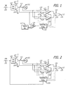
- FIG. 1 is an example of a motor 101 and a circuit for driving a winding of the motor 101 that may include a pulse-width-modulated (PWM) drive signal 103, a gate drive circuit 105, H-bridge switches 107 and 109, and a current sensing circuit.
- the current sensing circuit accurately measures current to the motor 101 and may include a shunt resistance 111, differential amplifiers 113 and 115, and a switching system that includes a threshold bias circuit 117, a comparator 119, a switch timing/nulling circuit 121, and electronic switches 123, 125, 127, 129, 131, and 133.
- the motor 101 may be of any type.
- the motor may be a DC motor whose torque is proportional to input current.
- the motor 101 may have several windings. Each winding may be driven by an additional instance of the circuit illustrated in FIG. 1 .
- the H-bridge switches 107 and 109 may be electronic switches, such as MOSFETs that may be driven at a switching frequency.
- the gate drive circuit 105 may be configured to actuate the H-bridge switches 107 and 109 so as to cause the winding of the motor 101 to be alternatingly connected to a high and a low voltage, such as to a positive supply voltage +V and to ground, in synchronism with state changes of the PWM drive signal 103.
- the gate drive circuit 105 may be configured to cause the winding of the motor 101 to be connected to +V when the PWM drive signal 103 is high and to ground when the PWM drive signal 103 is low.
- the PWM drive signal 103 may be generated by a drive circuit (not shown) that causes the PWM drive signal 103 to have a frequency and/or duty cycle that causes the motor 101 to operate in a particular desired way, such as at a particular position, speed, and/or acceleration. To facilitate this, information about the current that is traveling through the motor 101 may be needed by the drive circuit that generates the PWM drive signal 103. This current information may be obtained by measuring the voltage across the shunt resistance 111.
- the shunt resistance 111 may be a single resistor, a set of resistors, and/or one or more other types of components that have a resistance. The value of the resistance may be low, so as not to cause a large voltage drop and hence energy loss.
- the average of the voltage at the input of the shunt resistance 111 and the voltage at the output of the shunt resistance 111 is known as the common mode voltage.
- This common mode voltage may be very low when the motor winding is connected to ground through the H-bridge switch 109, while it may be very high when the motor winding is connected to +V through the H-bridge switch 107.
- Both differential amplifiers 113 and 115 may be configured to provide an amplified output of the voltage across the shunt resistance 111 when connected across the shunt resistance 111.
- the differential amplifier 113 may be optimized to provide its lowest output DC offset voltage when the common mode voltage is low (e.g., ground).
- the differential amplifier 115 may be optimized to provide its lowest output DC offset voltage when the common mode voltage is high (e.g., +V).
- both of the differential amplifiers 113 and 115 may have a small common mode rejection ratio, such as a ratio that is less than 40dB at the switching frequency.
- the switching system may be configured to cause a current sensing signal output 135 to be based on the amplified output of the first differential amplifier 113 and not the amplified output of the second differential amplifier 115 when the common mode voltage across the shunt resistance 111 is low (e.g., ground). Conversely, the switching system may be configured to cause the current sensing signal output 135 to be based on the amplified output of the second differential amplifier 115 and not the amplified output of the first differential amplifier 113 when the common mode voltage across the shunt resistance 111 is high (e.g., +V).
- Amplifiers 113 and 115 may each have connections to +V and GND, unlike as is illustrated in FIG. 1 . In that case, either may be used as the high common mode amplifier or the low common mode amplifier interchangeably.
- One amplifier might instead be connected to a low voltage, such as 5V and ground, while the other might instead be connected to +V and a voltage near +V, such as (+V - 5V).
- the amplifier tied to +V may serve as the high common mode voltage amplifier, while the one tied to ground may serve as the low common mode amplifier.
- the amplifier 113 When connected as shown in FIG. 1 , the amplifier 113 may be active when the common mode voltage is high, while the amplifier 115 may be active when the common mode voltage is low.
- the switching system may employ any means to facilitate this functionality.
- the threshold bias circuit 117 may generate a reference voltage and the comparator 119 may compare that reference voltage with a voltage on the shunt resistance 111, such as the voltage at the input to the shunt resistance 111.
- the output of the comparator 119 may cause the switch timing/nulling circuit 121 to cause the voltage across the shunt resistance 111 to be amplified by only the differential amplifier 113 by causing switches 123, 125, and 131 to close, while causing switches 127, 129, and 133 to open.
- the output of the comparator 119 may cause the switch timing/nulling circuit 121 to cause the voltage across the shunt resistance 111 to be amplified by only the differential amplifier 115 by causing switches 123, 125, and 131 to open, while causing switches 127, 129, and 133 to close.
- the switches 123, 125, 127, 129, 131, and 133 may be any type of electronic switches, such as MOSFETs.
- each may amplify the differential voltage across the shunt resistance 111 only when the differential amplifier is best matched to the common mode voltage of the shunt resistance 111, i.e., at a time when the common mode voltage is low (e.g., ground) for the differential amplifier 113 that is optimized for low common mode voltages, and at a time when the common mode voltage is high (e.g., +V) for the differential amplifier 115 that is optimized for high common mode voltages.
- the switch timing/nulling circuit 121 may automatically adjust the differential amplifiers 113 and 115 so as to cause their outputs to be zero when there is no differential voltage at their inputs.
- the switch timing/nulling circuit 121 may be configured to perform this function repeatedly during the course of the operation of the current sensing circuit, thereby compensating for drift in this zero output caused by temperature changes, component aging, and/or other reasons.
- the switch timing/nulling circuit 121 may implement any approach for effectuating this auto zeroing function.
- the switch timing/nulling circuit 121 may be configured to zero each of the differential amplifiers 113 and 115 when they are not being used to measure the voltage across the shunt resistance 111, e.g., when the input to the differential amplifier that is being nulled is disconnected from the shunt resistance 111 by opening the switches that connect the differential amplifier to the shunt resistance 111, thereby causing the voltage at the input of the differential amplifier to be zero.
- the switch timing/nulling circuit 121 may then examine the output of the disconnected differential amplifier and provide a compensating input to the differential amplifier that causes its output to also be at zero.
- Example of such nulling approaches may be found in U.S. patent 4,633,642 and European patent 1,428,314 . All or any portion of the switch timing/nulling circuit 121 could be part of the amplifiers 113 and/or 115.
- a clock that runs at a multiple of the frequency of the PWM drive signal 103 may be used to provide non-overlapping clocks.
- a PLL/frequency synthesizer or other type of circuit that can produce a multiple (e.g., doubling or quadrupling) of this frequency from the PWM drive signal 103 or from another signal may be used.
- the switch timing/nulling circuit 121 may instead be configured to null each of the differential amplifiers 113 and 115 while they are measuring the voltage across the shunt resistance 111. Examples of nulling approaches that may be used may be found in U.S. patent 7,292,095 ; " 140dB-CMMR Current-Feedback Instrumentation Amplifier Employing Ping-Pong Auto-Zeroing and Chopping," a paper presented at the 2009 IEEE International Solid-State Circuits Conference ; and " A Micro Power Chopper-Stabilized Operational Amplifier Using A SC Notch Filter With Synchronous Integration Inside The Continuous-Time Signal Path," IEEE Journal of Solid-State Circuits, Vol. 41, No. 12, Dec. 2006 .
- FIG. 2 is an example of the motor 101 and a circuit for driving a winding of the motor that includes a current sense circuit that is similar to the one in FIG. 1 , but that senses the common mode voltage indirectly, as compared to directly. Except as now described, the components in the circuit illustrated in FIG. 2 may be the same as those in FIG. 1 , as described above.
- the circuit in FIG. 2 may have a switch timing/nulling circuit 201 that senses the common mode voltage indirectly, as compared to directly. More specifically, the switch timing/nulling circuit 201 may utilize the PWM drive signal 103 to determine whether the common mode voltage across the shunt resistance 111 is high (e.g., +V) or low (e.g., ground). For example, it may deem each rising edge in the PWM drive signal 103 as indicating a change to a high common mode voltage (e.g., +V), while it may deem each falling edge in the PWM drive signal 103 as indicating a change to a low common mode voltage (e.g., ground). Except for this difference, the switch timing/nulling circuit 201 may be the same as the switch timing/nulling circuit 121 illustrated in FIG. 1 and discussed above.
- the switch timing/nulling circuit 201 may be the same as the switch timing/nulling circuit 121 illustrated in FIG. 1 and discussed above.
- FIG. 3 is an example of the motor 101 and a circuit for driving a winding of the motor that includes a current sense circuit that senses the common mode voltage both directly as in FIG. 1 and indirectly as in FIG. 2 . Except as now described, the components in the circuit illustrated in FIG. 3 may be the same as those in FIG. 1 , as described above.
- the circuit in FIG. 3 may have a switch timing/nulling circuit 301 that senses whether the common mode voltage is high (e.g., +V) or low (e.g., ground) based on both the output of the comparator 119 (a direct measurement) and the PWM drive signal 103 (an indirect measurement).
- the common mode voltage e.g., +V
- the PWM drive signal 103 an indirect measurement
- the switch timing/nulling circuit 301 may switch in the differential amplifier 113 so that it can begin measuring the voltage across the shunt resistance 111 when the voltage on the shunt resistance 111 drops below the voltage produced by the threshold bias circuit 117; may switch out the differential amplifier 113 so that it stops measuring the voltage across the shunt resistance 111 when there is an upward transition in the PWM drive signal 103; may switch in the differential amplifier 115 so that it begins measuring the voltage across the shunt resistance 111 when the voltage on the shunt resistance 111 rises above the voltage produced by the threshold bias circuit 117; and may switch out the differential amplifier 115 so that it stops measuring the voltage across the shunt resistance 111 when there is a downward transition in the PWM drive signal 103. Except for this difference, the switch timing/nulling circuit 301 may be the same as the switch timing/nulling circuit 121 illustrated in FIG. 1 and discussed above.
- FIG. 4 is an example of the motor 101 and a circuit for driving a winding of the motor 101 that includes a current sense circuit that is similar to the one in FIG. 1 , but that uses two comparators to sense whether the common mode voltage is high or low, as compared to a single comparator. Except as now described, the components in the circuit illustrated in FIG. 4 may be the same as those in FIG. 1 , as described above.
- a threshold bias circuit 403 may generate both a high reference voltage 405 and a low reference voltage 407.
- the high reference voltage 405 may be compared by a comparator 409 with the voltage on the shunt resistance 111.
- the low reference voltage 407 may be compared by a comparator 411 with a voltage on the shunt resistance 111.
- a switch timing/nulling circuit 401 may be configured to control the switches 123, 125, 127, 129, 131, and 133 in the same manner as the switch timing/nulling circuit 121.
- the switch timing/nulling circuit 401 may be configured not to switch in the differential amplifier 113 until the voltage on the shunt resistance 111 drops below the low reference voltage 407, as signaled by the comparator 411. Similarly, the switch timing/nulling circuit 401 may be configured not to switch in the differential amplifier 115 until the voltage on the shunt resistance 111 rises above the high reference voltage 405, as signaled by the comparator 409. The switch timing/nulling circuit 401 may be configured to disconnect both differential amplifiers 113 and 115 during a brief period of time when the voltage on the shunt resistance 111 transitions between the low reference voltage 407 and the high reference voltage 405, as signaled by comparators 409 and 411. Except for this difference, the switch timing/nulling circuit 401 may be the same as the switch timing/nulling circuit 121 illustrated in FIG. 1 and discussed above.
- FIG. 5 is an example of the motor 101 and a circuit for driving a winding of the motor 101 that includes a current sense circuit that combines the dual comparator feature of the circuit shown in FIG. 4 with the dual input signals of FIG. 3 . Except as now described, the components in the circuit illustrated in FIG. 5 may be the same as those in FIGS. 3 and 4 , as described above.
- a switch timing/nulling circuit 501 may be configured to switch in the differential amplifier 113 so that it can begin measuring the voltage across the shunt resistance 111 when the voltage on the shunt resistance 111 drops below the low reference voltage 407 as detected by the comparator 411; may switch out the differential amplifier 113 so that it stops measuring the voltage across the shunt resistance 111 when there is an upward transition in the PWM drive signal 103; may switch in the differential amplifier 115 so that it begins measuring the voltage across the shunt resistance 111 when the voltage on the shunt resistance 111 rises above the high reference voltage 405 as detected by the comparator 409; and may switch out the differential amplifier 115 so that it stops measuring the voltage across the shunt resistance 111 when there is a downward transition in the PWM drive signal 103. Except for this difference, the switch timing/nulling circuit 501 may be the same as the switch timing/nulling circuit 121 illustrated in FIG. 1 and discussed above.
- FIG. 6 is an example of the motor 101 and a circuit for driving a winding of the motor 101 that includes a current sense circuit that is similar to the one in FIG. 5 , but that uses sample and hold circuits 603 and 605 to preserve the inputs to the differential amplifiers 113 and 115. Except as now described, the components in the circuit illustrated in FIG. 6 may be the same as those in FIG. 5 , as described above.
- a switch timing/nulling circuit 601 may be configured to control the sample and hold circuits 603 and 605 so as to cause them to each sample the voltage across the shunt resistance 111 at the end of the period when the differential amplifier to which the sample and hold circuit is amplifying the voltage across the shunt resistance 111.
- the switch timing/nulling circuit 601 may be configured to control the sample and hold circuits 603 and 605 so as to cause them to each hold that sampled voltage at the input to its differential amplifier while its differential amplifier is not amplifying the voltage across the shunt resistance 111. Except for this additional functionality, the switch timing/nulling circuit 601 may be the same as the switch timing/nulling circuit 501.
- a track and hold circuit may be used instead of one or both of the sample and hold circuits 603 and 605.
- the voltage on the shunt resistance 111 may first be attenuated using, for example, a resistive divider, so that a lower threshold voltage may be applied to the comparator reference input.
- the differential amplifiers may be configured such that the switch timing/nulling circuit can set the output of a differential amplifier in a high-impedance state, so that the output 135 of the circuit may be derived, in turn, from the differential amplifier which is not set in a high-impedance state, using a technique commonly referred to as "wired-or" connecting of two outputs.
- Comparators may also be used to detect fault conditions, such as a disconnected sense resistance or a shorted winding.
- the amplifiers may be designed such that the inputs must stay within the supplies, or such that the inputs may operate outside of the supplies, allowing for supply voltages that are substantially lower than the motor winding voltages.
- the amplifiers may operate from the same set of power supplies, or power supplies tailored to the common-mode voltages that correspond to the active periods of each amplifier's operation.
- the amplifiers may null at frequencies that are higher than, lower than, or synchronized to the common-mode switch frequency. The nulling may include spread-spectrum or other clock-feed through reduction techniques.
Landscapes
- Engineering & Computer Science (AREA)
- Power Engineering (AREA)
- Physics & Mathematics (AREA)
- General Physics & Mathematics (AREA)
- Control Of Direct Current Motors (AREA)
- Measurement Of Current Or Voltage (AREA)
- Amplifiers (AREA)
Claims (15)
- Strommessschaltung, umfassend:einen Nebenwiderstand (111), durch den zu messender Strom fließt;einen ersten Differenzverstärker (113), welcher einen verstärkten Ausgang der Spannung über den Nebenwiderstand (111) bereitstellt und welcher für niedrige Gleichtaktspannungen optimiert ist;einen zweiten Differenzverstärker (115), welcher einen verstärkten Ausgang der Spannung über den Nebenwiderstand (111) bereitstellt und welcher nicht der erste Differenzverstärker (113) ist und welcher für hohe Gleichtaktspannungen optimiert ist; undein Schaltsystem (121, 123, 125, 127, 129, 131, 13), welches einen Strommesssignalausgang (135) ausgibt, basierend auf:dem verstärkten Ausgang des ersten Differenzverstärkers und nicht dem verstärkten Ausgang des zweiten Differenzverstärkers, wenn die Gleichtaktspannung des Nebenwiderstands niedrig ist; unddem verstärkten Ausgang des zweiten Differenzverstärkers und nicht dem verstärkten Ausgang des ersten Differenzverstärkers, wenn die Gleichtaktspannung des Nebenwiderstands hoch ist,wobei die Größe der Gleichtaktspannung bestimmt, wann und wie das Schalten durch das Schaltsystem erfolgt.
- Strommessschaltung nach Anspruch 1, wobei:
die Strommessschaltung Strom misst, welcher durch einen oder mehrere Schalter gesteuert oder geregelt ist, welche mit einer Schaltfrequenz schalten, und der erste und der zweite Differenzverstärker beide ein Gleichtaktunterdrückungsverhältnis von weniger als 40 dB bei der Schaltfrequenz haben; und/oder wobei:der erste Differenzverstärker (113) seine niedrigste ausgegebene Gleichspannungs-Offsetspannung bereitstellt, wenn die Gleichtaktspannung niedrig ist und nicht, wenn sie hoch ist; undder zweite Differenzverstärker (115) seine niedrigste ausgegebene Gleichspannungs-Offsetspannung bereitstellt, wenn die Gleichtaktspannung hoch ist und nicht, wenn sie niedrig ist. - Strommessschaltung nach Anspruch 1 oder 2, wobei das Schaltsystem den Differenzverstärker, auf dem sie den Strommesssignalausgang basiert, basierend auf einem Vergleich einer Spannung an dem Nebenwiderstand (111) mit einer Referenzspannung ändert; vorzugsweise wobei das Schaltsystem das Strommesssignalausgang basiert auf:den verstärkten Ausgang des ersten Differenzverstärkers (113) und nicht den verstärkten Ausgang des zweiten Differenzverstärkers (115), wenn die Spannung über dem Nebenwiderstand (111) kleiner als eine niedrige Referenzspannung ist; undden verstärkten Ausgang des zweiten Differenzverstärkers (115) und nicht den verstärkten Ausgang des ersten Differenzverstärkers (113), wenn die Spannung über dem Nebenwiderstand (111) größer als eine hohe Referenzspannung ist, welche höher als die niedrige Referenzspannung ist.
- Strommessschaltung nach einem der Ansprüche 1 bis 3, ferner umfassend:eine erste Halte-Schaltung (603), welche den Wert einer Spannung an dem Nebenwiderstand (111) hält, wenn die Gleichtaktspannung des Nebenwiederstands niedrig ist, während die Gleichtaktspannung des Nebenwiderstands hoch ist; undeine zweite Halte-Schaltung (605), welche den Wert einer Spannung an dem Nebenwiderstand (111) hält, wenn die Gleichtaktspannung des Nebenwiderstands hoch ist, während die Gleichtaktspannung des Nebenwiderstands niedrig ist.
- Strommessschaltung nach einem der Ansprüche 1 bis 4, wobei die Messschaltung zum Messen des Stroms verwendet wird, welcher durch eine H-Brücke (107, 109) abgegeben wird, welche durch ein Schaltsignal angesteuert ist, und wobei das Schaltsystem den Differenzverstärker, auf den es den Strommesssignalausgang basiert, basierend auf dem Schaltsignal ändert.
- Strommessschaltung nach Anspruch 5, wobei das Schaltsystem ferner den Differenzverstärker, auf den es den Strommesssignalausgang basiert, basierend auf einem Vergleich einer Spannung an einem Anschluss des Nebenwiderstands mit einer Referenzspannung ändert.
- Strommessschaltung nach Anspruch 6, wobei das Schaltsystem ferner den Strommesssignalausgang basiert auf:den verstärkten Ausgang des ersten Differenzverstärkers (113) und nicht den verstärkten Ausgang des zweiten Differenzverstärkers (115), wenn die Spannung an einem Anschluss des Nebenwiderstands kleiner als eine niedrige Referenzspannung ist; undden verstärkten Ausgang des zweiten Differenzverstärkers (115) und nicht den verstärkten Ausgang des ersten Differenzverstärkers (113), wenn die Spannung an einem Anschluss des Nebenwiderstands (111) größer als eine hohe Referenzspannung ist, welche höher als die niedrige Referenzspannung ist.
- Strommessschaltung nach Anspruch 6 oder 7, wobei das Schaltsystem:das Basieren des Strommesssignalausgangs auf den verstärkten Ausgang des ersten Differenzverstärkers (113) beginnt, wenn die Spannung an einem Anschluss des Nebenwiderstands (111) kleiner als eine erste Referenzspannung ist; unddas Basieren des Strommesssignalausgangs auf den verstärkten Ausgang des ersten Differenzverstärkers (113) beendet, wenn ein Übergang in dem Schaltsignal vorliegt;das Basieren des Strommesssignalausgangs auf den verstärkten Ausgang des zweiten Differenzverstärkers (115) beginnt, wenn die Spannung an einem Anschluss des Nebenwiderstands größer als eine zweite Referenzspannung ist; unddas Basieren des Strommesssignalausgangs auf den verstärkten Ausgang des zweiten Differenzverstärkers (115) beendet, wenn ein Übergang in dem Schaltsignal vorliegt.
- Strommessschaltung nach Anspruch 8, wobei:die erste und die zweite Referenzspannung die gleichen sind; oderdie erste Referenzspannung niedriger als die zweite Referenzspannung ist.
- Strommessschaltung nach einem der Ansprüche 1 bis 9, wobei das Schaltsystem einen oder mehrere elektronische Schalter (131, 133) enthält, welche den Strommesssignalausgang zwischen dem verstärkten Ausgang des ersten Differenzverstärkers (113) und dem verstärkten Ausgang des zweiten Differenzverstärkers (115) schalten.
- Strommessschaltung nach einem der Ansprüche 1 bis 10, wobei:der erste Differenzverstärker (113) einen Eingang hat;der zweite Differenzverstärker (115) einen Eingang hat; unddas Schaltsystem einen oder mehrere elektronische Schalter (123, 125, 127, 129) enthält, welche die Spannungen an den Anschlüssen des Nebenwiderstands (111) zwischen den Eingängen des ersten und des zweiten Differenzverstärkers schalten.
- Strommessschaltung nach Anspruch 11, ferner umfassend:eine erste Halte-Schaltung (603), welche den Wert der Spannungen an dem Eingang zu dem ersten Differenzverstärker (113) behält, wenn sie auf den Eingang des ersten Differenzverstärkers geschaltet ist, nachdem sie auf den Eingang des zweiten Differenzverstärkers (115) geschaltet ist; undeine zweite Halteschaltung (605), welche den Wert der Spannungen an dem Eingang zu dem zweiten Differenzverstärker (115) behält, wenn sie auf den Eingang des zweiten Differenzverstärkers geschaltet ist, nachdem sie auf den Eingang des ersten Differenzverstärkers (113) geschaltet ist; und/oderwobei das Schaltsystem einen oder mehrere elektronische Schalter (131, 133) enthält, welche den Strommesssignalausgang zwischen dem verstärkten Ausgang des ersten Differenzverstärkers und dem verstärkten Ausgang des zweiten Differenzverstärkers schalten.
- Strommessschaltung nach einem der Ansprüche 1 bis 12 ferner umfassend eine Nullungsschaltung (121), welche den ersten und den zweiten Differenzverstärker so einstellt, dass ihre jeweiligen verstärkten Ausgänge im Wesentlichen Null sind, wenn die Spannung über dem Nebenwiderstand im Wesentlichen Null ist.
- Strommessschaltung nach Anspruch 13, wobei die Nullungsschaltung:den ersten Differenzverstärker (113) einstellt, wenn der Strommesssignalausgang auf dem Ausgang des zweiten Differenzverstärkers (115) basiert ist; undden zweiten Differenzverstärker einstellt, wenn der Strommesssignalausgang auf dem Ausgang des ersten Differenzverstärkers basiert ist; und/oderwobei die Nullungsschaltung den ersten und den zweiten Differenzverstärker im Wesentlichen zur gleichen Zeit einstellt.
- Strommessschaltung nach Anspruch 1, welche zum Antreiben einer Wicklung eines Motors verwendet wird, ferner umfassend eine H-Brücke von Schaltern (107, 109); und wobei
der Nebenwiderstand (111) zwischen der H-Brücke von Schaltern und der Wicklung des Motors ist.
Applications Claiming Priority (2)
| Application Number | Priority Date | Filing Date | Title |
|---|---|---|---|
| US201361866334P | 2013-08-15 | 2013-08-15 | |
| US14/148,550 US9240718B2 (en) | 2013-08-15 | 2014-01-06 | Accurate current sensing in H-bridge applications without amplifier having high common mode rejection ratio |
Publications (2)
| Publication Number | Publication Date |
|---|---|
| EP2840407A1 EP2840407A1 (de) | 2015-02-25 |
| EP2840407B1 true EP2840407B1 (de) | 2019-07-31 |
Family
ID=51352384
Family Applications (1)
| Application Number | Title | Priority Date | Filing Date |
|---|---|---|---|
| EP14002828.3A Active EP2840407B1 (de) | 2013-08-15 | 2014-08-13 | Genaue Strommessung in H-Brücken-Anwendungen ohne Verstärker mit hohem Gleichtaktunterdrückungsverhältnis |
Country Status (4)
| Country | Link |
|---|---|
| US (1) | US9240718B2 (de) |
| EP (1) | EP2840407B1 (de) |
| JP (1) | JP6215795B2 (de) |
| KR (1) | KR102186206B1 (de) |
Families Citing this family (15)
| Publication number | Priority date | Publication date | Assignee | Title |
|---|---|---|---|---|
| US9547354B2 (en) * | 2013-04-11 | 2017-01-17 | Dell Products L.P. | System and method for increasing current monitor power telemetry accuracy |
| US9240718B2 (en) | 2013-08-15 | 2016-01-19 | Linear Technology Corporation | Accurate current sensing in H-bridge applications without amplifier having high common mode rejection ratio |
| ITUA20163209A1 (it) * | 2016-05-06 | 2017-11-06 | St Microelectronics Srl | Dispositivo di misura di corrente in un carico induttivo |
| KR102612239B1 (ko) * | 2016-09-12 | 2023-12-12 | 에이치엘만도 주식회사 | 모터 제어 장치 및 방법 |
| CN106599754B (zh) * | 2017-01-16 | 2023-08-11 | 深圳市傲科光电子有限公司 | 一种lid读写器及其跨阻放大电路 |
| JP6971048B2 (ja) * | 2017-04-05 | 2021-11-24 | 新日本無線株式会社 | 電流センス回路 |
| US10917092B2 (en) * | 2018-04-06 | 2021-02-09 | Allegro Microsystems, Llc | Magnetic field sensor with switching network |
| CN109194218B (zh) * | 2018-09-07 | 2020-02-14 | 华中科技大学 | 直流偏置型混合励磁电机的控制装置、控制方法及系统 |
| US11169218B2 (en) * | 2018-12-21 | 2021-11-09 | Analog Devices, Inc. | Current monitor with fault detection |
| KR102723875B1 (ko) * | 2019-01-23 | 2024-10-30 | 에이치엘만도 주식회사 | 전동 파워스티어링용 모터의 전류 검출 장치 |
| KR102449930B1 (ko) * | 2021-02-08 | 2022-10-05 | 한국자동차연구원 | 팬터그래프 접촉저항 측정 장치 |
| JP7666866B2 (ja) * | 2021-04-22 | 2025-04-22 | 東京エレクトロン株式会社 | デバイス検査装置及びデバイス検査方法 |
| DE112023001219T5 (de) * | 2022-03-03 | 2025-01-16 | Asahi Kasei Microdevices Corporation | Stromsensor und Stromerkennungsverfahren |
| CN115452184A (zh) * | 2022-08-21 | 2022-12-09 | 河南嘉晨智能控制股份有限公司 | 一种基于热敏电阻的精确地温度检测方法 |
| CN120567070B (zh) * | 2025-07-29 | 2025-11-25 | 江苏润石科技有限公司 | 一种高共模抑制比精密电流检测放大器 |
Family Cites Families (21)
| Publication number | Priority date | Publication date | Assignee | Title |
|---|---|---|---|---|
| US2873417A (en) * | 1955-04-06 | 1959-02-10 | Floyd V Wilkins | Adjustable-speed electric motor control system |
| US4535276A (en) * | 1983-01-12 | 1985-08-13 | Matsushita Electric Industrial Co., Ltd. | Output circuit and brushless motor using the same |
| IT8423459U1 (it) | 1984-10-05 | 1986-04-05 | S I A T Soc Internazionale Applicazioni Tecniche S P A | Dispositivo a rulli di pressione per il ritegno laterale delle scatole, in macchine da imballaggio con avanzamento automatico delle scatole |
| US4764720A (en) * | 1985-12-05 | 1988-08-16 | Load Controls Incorporated | Apparatus and method for measuring variable frequency power |
| US4933642A (en) | 1989-02-17 | 1990-06-12 | Linear Technology Corporation | CMOS chopper-stabilized operational amplifier using two differential amplifier pairs as input stages |
| US5266888A (en) * | 1992-02-28 | 1993-11-30 | The Narda Microwave Corp. | Wide power range radiation monitor |
| JPH07251749A (ja) * | 1994-03-16 | 1995-10-03 | Mitsubishi Electric Corp | 電動パワーステアリング制御装置 |
| JP3154665B2 (ja) | 1996-08-29 | 2001-04-09 | 三菱電機株式会社 | ハイサイド方式のモータ電流検出回路 |
| US5920189A (en) * | 1996-11-26 | 1999-07-06 | Delco Electronics Corporation | Auto ranging current monitor with common mode correction |
| US5861775A (en) * | 1997-01-16 | 1999-01-19 | Ford Global Technologies, Inc. | Signal conditioning circuit for low amplitude, high common mode voltage input signals |
| WO1998058833A1 (fr) * | 1997-06-20 | 1998-12-30 | Mitsubishi Denki Kabushiki Kaisha | Dispositif de direction assistee entraine par un moteur electrique |
| US6570360B1 (en) * | 1999-06-30 | 2003-05-27 | Seagate Technology Llc | Self-synchronizing AC synchronous driver for DC brushless motors |
| JP2002002514A (ja) * | 2000-06-16 | 2002-01-09 | Unisia Jecs Corp | 電動モータ駆動式操舵補助装置の異常判定装置 |
| US6476671B1 (en) | 2001-09-04 | 2002-11-05 | Analog Devices, Inc. | Ping-pong amplifier with auto-zeroing and chopping |
| DE102004036352B4 (de) * | 2004-05-27 | 2007-10-25 | Atmel Germany Gmbh | Schaltkreis zur Strommessung und Stromüberwachung und deren Verwendung für eine Funktionseinheit |
| JP4246679B2 (ja) | 2004-08-27 | 2009-04-02 | 株式会社日立製作所 | 電流検出装置 |
| US7292095B2 (en) | 2006-01-26 | 2007-11-06 | Texas Instruments Incorporated | Notch filter for ripple reduction in chopper stabilized amplifiers |
| US7224135B1 (en) * | 2006-09-07 | 2007-05-29 | Acutechnology Semiconductor Inc. | Imposed current motor drive |
| US20130009655A1 (en) * | 2011-03-01 | 2013-01-10 | Sendyne Corporation | Current sensor |
| JP5726012B2 (ja) | 2011-08-02 | 2015-05-27 | オムロンオートモーティブエレクトロニクス株式会社 | モータ制御装置 |
| US9240718B2 (en) | 2013-08-15 | 2016-01-19 | Linear Technology Corporation | Accurate current sensing in H-bridge applications without amplifier having high common mode rejection ratio |
-
2014
- 2014-01-06 US US14/148,550 patent/US9240718B2/en active Active
- 2014-08-13 KR KR1020140105100A patent/KR102186206B1/ko active Active
- 2014-08-13 EP EP14002828.3A patent/EP2840407B1/de active Active
- 2014-08-14 JP JP2014165126A patent/JP6215795B2/ja active Active
Non-Patent Citations (1)
| Title |
|---|
| None * |
Also Published As
| Publication number | Publication date |
|---|---|
| JP2015045640A (ja) | 2015-03-12 |
| EP2840407A1 (de) | 2015-02-25 |
| US9240718B2 (en) | 2016-01-19 |
| KR20150020121A (ko) | 2015-02-25 |
| US20150048770A1 (en) | 2015-02-19 |
| KR102186206B1 (ko) | 2020-12-04 |
| JP6215795B2 (ja) | 2017-10-18 |
Similar Documents
| Publication | Publication Date | Title |
|---|---|---|
| EP2840407B1 (de) | Genaue Strommessung in H-Brücken-Anwendungen ohne Verstärker mit hohem Gleichtaktunterdrückungsverhältnis | |
| CN107942251B (zh) | 电流检测系统、方法和电流检测装置 | |
| JP4924086B2 (ja) | 半導体装置 | |
| US8547064B2 (en) | Battery cell tab monitor | |
| US9294049B2 (en) | Fast-settling capacitive-coupled amplifiers | |
| CN100355196C (zh) | 小电枢电感高速永磁无刷直流电动机无位置传感器控制系统 | |
| CN102891644B (zh) | 一种两相步进电机驱动电路及电机故障检测方法 | |
| US10421367B2 (en) | Electric vehicle battery test | |
| EP3176593A1 (de) | Elektromotorische halleffekt-kraftsignaldetektionsschaltung und stromsensor | |
| KR101542679B1 (ko) | 자기 검출 장치 및 자기 검출 방법 | |
| US10784810B1 (en) | Motor controller with accurate current measurement | |
| US20130222001A1 (en) | Current sensor having self-diagnosis function and signal processing circuit | |
| US20080157752A1 (en) | Current Sensor and Method for Motor Control | |
| CN101800509B (zh) | 永磁式同步马达的转子位置检测装置及方法 | |
| EP3026446B1 (de) | Elektrisches stromsystem mit spannungsabfallkomponente | |
| US11079458B2 (en) | Voltage sensor diagnosis device and voltage sensor diagnosis method | |
| JP2013102283A (ja) | 電流出力回路 | |
| JP3691364B2 (ja) | 電流検出装置と電流検出装置を備えるバッテリー装置 | |
| CN102971634B (zh) | 确定测量信道的修正参数和检测电动机的端子电压的方法或电压检测系统 | |
| US11165374B2 (en) | Sensor-less circuits and related methods for back EMF zero crossing detection | |
| JP2009180693A (ja) | 電流センサと電子制御ユニットとの間の断線検知システム | |
| JP6016346B2 (ja) | セルテレメトリーのためのサンプルホールドアンプ | |
| CN202906821U (zh) | 一种两相步进电机驱动电路 | |
| EP2809004A1 (de) | Nanovoltverstärkerschaltung | |
| CN117310476A (zh) | 继电器检测电路、方法以及车辆 |
Legal Events
| Date | Code | Title | Description |
|---|---|---|---|
| PUAI | Public reference made under article 153(3) epc to a published international application that has entered the european phase |
Free format text: ORIGINAL CODE: 0009012 |
|
| 17P | Request for examination filed |
Effective date: 20140813 |
|
| AK | Designated contracting states |
Kind code of ref document: A1 Designated state(s): AL AT BE BG CH CY CZ DE DK EE ES FI FR GB GR HR HU IE IS IT LI LT LU LV MC MK MT NL NO PL PT RO RS SE SI SK SM TR |
|
| AX | Request for extension of the european patent |
Extension state: BA ME |
|
| R17P | Request for examination filed (corrected) |
Effective date: 20150821 |
|
| RBV | Designated contracting states (corrected) |
Designated state(s): AL AT BE BG CH CY CZ DE DK EE ES FI FR GB GR HR HU IE IS IT LI LT LU LV MC MK MT NL NO PL PT RO RS SE SI SK SM TR |
|
| GRAP | Despatch of communication of intention to grant a patent |
Free format text: ORIGINAL CODE: EPIDOSNIGR1 |
|
| STAA | Information on the status of an ep patent application or granted ep patent |
Free format text: STATUS: GRANT OF PATENT IS INTENDED |
|
| INTG | Intention to grant announced |
Effective date: 20190221 |
|
| GRAS | Grant fee paid |
Free format text: ORIGINAL CODE: EPIDOSNIGR3 |
|
| GRAA | (expected) grant |
Free format text: ORIGINAL CODE: 0009210 |
|
| STAA | Information on the status of an ep patent application or granted ep patent |
Free format text: STATUS: THE PATENT HAS BEEN GRANTED |
|
| AK | Designated contracting states |
Kind code of ref document: B1 Designated state(s): AL AT BE BG CH CY CZ DE DK EE ES FI FR GB GR HR HU IE IS IT LI LT LU LV MC MK MT NL NO PL PT RO RS SE SI SK SM TR |
|
| REG | Reference to a national code |
Ref country code: CH Ref legal event code: EP Ref country code: GB Ref legal event code: FG4D |
|
| REG | Reference to a national code |
Ref country code: AT Ref legal event code: REF Ref document number: 1161483 Country of ref document: AT Kind code of ref document: T Effective date: 20190815 |
|
| REG | Reference to a national code |
Ref country code: IE Ref legal event code: FG4D |
|
| REG | Reference to a national code |
Ref country code: DE Ref legal event code: R096 Ref document number: 602014050740 Country of ref document: DE |
|
| REG | Reference to a national code |
Ref country code: CH Ref legal event code: NV Representative=s name: PATENTANWAELTE SCHAAD, BALASS, MENZL AND PARTN, CH |
|
| REG | Reference to a national code |
Ref country code: NL Ref legal event code: MP Effective date: 20190731 |
|
| REG | Reference to a national code |
Ref country code: LT Ref legal event code: MG4D |
|
| REG | Reference to a national code |
Ref country code: AT Ref legal event code: MK05 Ref document number: 1161483 Country of ref document: AT Kind code of ref document: T Effective date: 20190731 |
|
| PG25 | Lapsed in a contracting state [announced via postgrant information from national office to epo] |
Ref country code: PT Free format text: LAPSE BECAUSE OF FAILURE TO SUBMIT A TRANSLATION OF THE DESCRIPTION OR TO PAY THE FEE WITHIN THE PRESCRIBED TIME-LIMIT Effective date: 20191202 Ref country code: FI Free format text: LAPSE BECAUSE OF FAILURE TO SUBMIT A TRANSLATION OF THE DESCRIPTION OR TO PAY THE FEE WITHIN THE PRESCRIBED TIME-LIMIT Effective date: 20190731 Ref country code: NO Free format text: LAPSE BECAUSE OF FAILURE TO SUBMIT A TRANSLATION OF THE DESCRIPTION OR TO PAY THE FEE WITHIN THE PRESCRIBED TIME-LIMIT Effective date: 20191031 Ref country code: NL Free format text: LAPSE BECAUSE OF FAILURE TO SUBMIT A TRANSLATION OF THE DESCRIPTION OR TO PAY THE FEE WITHIN THE PRESCRIBED TIME-LIMIT Effective date: 20190731 Ref country code: LT Free format text: LAPSE BECAUSE OF FAILURE TO SUBMIT A TRANSLATION OF THE DESCRIPTION OR TO PAY THE FEE WITHIN THE PRESCRIBED TIME-LIMIT Effective date: 20190731 Ref country code: AT Free format text: LAPSE BECAUSE OF FAILURE TO SUBMIT A TRANSLATION OF THE DESCRIPTION OR TO PAY THE FEE WITHIN THE PRESCRIBED TIME-LIMIT Effective date: 20190731 Ref country code: HR Free format text: LAPSE BECAUSE OF FAILURE TO SUBMIT A TRANSLATION OF THE DESCRIPTION OR TO PAY THE FEE WITHIN THE PRESCRIBED TIME-LIMIT Effective date: 20190731 Ref country code: SE Free format text: LAPSE BECAUSE OF FAILURE TO SUBMIT A TRANSLATION OF THE DESCRIPTION OR TO PAY THE FEE WITHIN THE PRESCRIBED TIME-LIMIT Effective date: 20190731 Ref country code: BG Free format text: LAPSE BECAUSE OF FAILURE TO SUBMIT A TRANSLATION OF THE DESCRIPTION OR TO PAY THE FEE WITHIN THE PRESCRIBED TIME-LIMIT Effective date: 20191031 |
|
| PG25 | Lapsed in a contracting state [announced via postgrant information from national office to epo] |
Ref country code: GR Free format text: LAPSE BECAUSE OF FAILURE TO SUBMIT A TRANSLATION OF THE DESCRIPTION OR TO PAY THE FEE WITHIN THE PRESCRIBED TIME-LIMIT Effective date: 20191101 Ref country code: LV Free format text: LAPSE BECAUSE OF FAILURE TO SUBMIT A TRANSLATION OF THE DESCRIPTION OR TO PAY THE FEE WITHIN THE PRESCRIBED TIME-LIMIT Effective date: 20190731 Ref country code: AL Free format text: LAPSE BECAUSE OF FAILURE TO SUBMIT A TRANSLATION OF THE DESCRIPTION OR TO PAY THE FEE WITHIN THE PRESCRIBED TIME-LIMIT Effective date: 20190731 Ref country code: IS Free format text: LAPSE BECAUSE OF FAILURE TO SUBMIT A TRANSLATION OF THE DESCRIPTION OR TO PAY THE FEE WITHIN THE PRESCRIBED TIME-LIMIT Effective date: 20191130 Ref country code: RS Free format text: LAPSE BECAUSE OF FAILURE TO SUBMIT A TRANSLATION OF THE DESCRIPTION OR TO PAY THE FEE WITHIN THE PRESCRIBED TIME-LIMIT Effective date: 20190731 Ref country code: ES Free format text: LAPSE BECAUSE OF FAILURE TO SUBMIT A TRANSLATION OF THE DESCRIPTION OR TO PAY THE FEE WITHIN THE PRESCRIBED TIME-LIMIT Effective date: 20190731 |
|
| PG25 | Lapsed in a contracting state [announced via postgrant information from national office to epo] |
Ref country code: TR Free format text: LAPSE BECAUSE OF FAILURE TO SUBMIT A TRANSLATION OF THE DESCRIPTION OR TO PAY THE FEE WITHIN THE PRESCRIBED TIME-LIMIT Effective date: 20190731 |
|
| PG25 | Lapsed in a contracting state [announced via postgrant information from national office to epo] |
Ref country code: RO Free format text: LAPSE BECAUSE OF FAILURE TO SUBMIT A TRANSLATION OF THE DESCRIPTION OR TO PAY THE FEE WITHIN THE PRESCRIBED TIME-LIMIT Effective date: 20190731 Ref country code: IT Free format text: LAPSE BECAUSE OF FAILURE TO SUBMIT A TRANSLATION OF THE DESCRIPTION OR TO PAY THE FEE WITHIN THE PRESCRIBED TIME-LIMIT Effective date: 20190731 Ref country code: PL Free format text: LAPSE BECAUSE OF FAILURE TO SUBMIT A TRANSLATION OF THE DESCRIPTION OR TO PAY THE FEE WITHIN THE PRESCRIBED TIME-LIMIT Effective date: 20190731 Ref country code: DK Free format text: LAPSE BECAUSE OF FAILURE TO SUBMIT A TRANSLATION OF THE DESCRIPTION OR TO PAY THE FEE WITHIN THE PRESCRIBED TIME-LIMIT Effective date: 20190731 Ref country code: EE Free format text: LAPSE BECAUSE OF FAILURE TO SUBMIT A TRANSLATION OF THE DESCRIPTION OR TO PAY THE FEE WITHIN THE PRESCRIBED TIME-LIMIT Effective date: 20190731 |
|
| PG25 | Lapsed in a contracting state [announced via postgrant information from national office to epo] |
Ref country code: CZ Free format text: LAPSE BECAUSE OF FAILURE TO SUBMIT A TRANSLATION OF THE DESCRIPTION OR TO PAY THE FEE WITHIN THE PRESCRIBED TIME-LIMIT Effective date: 20190731 Ref country code: SM Free format text: LAPSE BECAUSE OF FAILURE TO SUBMIT A TRANSLATION OF THE DESCRIPTION OR TO PAY THE FEE WITHIN THE PRESCRIBED TIME-LIMIT Effective date: 20190731 Ref country code: MC Free format text: LAPSE BECAUSE OF FAILURE TO SUBMIT A TRANSLATION OF THE DESCRIPTION OR TO PAY THE FEE WITHIN THE PRESCRIBED TIME-LIMIT Effective date: 20190731 Ref country code: IS Free format text: LAPSE BECAUSE OF FAILURE TO SUBMIT A TRANSLATION OF THE DESCRIPTION OR TO PAY THE FEE WITHIN THE PRESCRIBED TIME-LIMIT Effective date: 20200224 Ref country code: LU Free format text: LAPSE BECAUSE OF NON-PAYMENT OF DUE FEES Effective date: 20190813 Ref country code: SK Free format text: LAPSE BECAUSE OF FAILURE TO SUBMIT A TRANSLATION OF THE DESCRIPTION OR TO PAY THE FEE WITHIN THE PRESCRIBED TIME-LIMIT Effective date: 20190731 |
|
| REG | Reference to a national code |
Ref country code: BE Ref legal event code: MM Effective date: 20190831 |
|
| REG | Reference to a national code |
Ref country code: DE Ref legal event code: R097 Ref document number: 602014050740 Country of ref document: DE |
|
| PLBE | No opposition filed within time limit |
Free format text: ORIGINAL CODE: 0009261 |
|
| STAA | Information on the status of an ep patent application or granted ep patent |
Free format text: STATUS: NO OPPOSITION FILED WITHIN TIME LIMIT |
|
| PG2D | Information on lapse in contracting state deleted |
Ref country code: IS |
|
| PG25 | Lapsed in a contracting state [announced via postgrant information from national office to epo] |
Ref country code: IE Free format text: LAPSE BECAUSE OF NON-PAYMENT OF DUE FEES Effective date: 20190813 Ref country code: IS Free format text: LAPSE BECAUSE OF FAILURE TO SUBMIT A TRANSLATION OF THE DESCRIPTION OR TO PAY THE FEE WITHIN THE PRESCRIBED TIME-LIMIT Effective date: 20191030 |
|
| 26N | No opposition filed |
Effective date: 20200603 |
|
| PG25 | Lapsed in a contracting state [announced via postgrant information from national office to epo] |
Ref country code: BE Free format text: LAPSE BECAUSE OF NON-PAYMENT OF DUE FEES Effective date: 20190831 Ref country code: SI Free format text: LAPSE BECAUSE OF FAILURE TO SUBMIT A TRANSLATION OF THE DESCRIPTION OR TO PAY THE FEE WITHIN THE PRESCRIBED TIME-LIMIT Effective date: 20190731 |
|
| REG | Reference to a national code |
Ref country code: DE Ref legal event code: R082 Ref document number: 602014050740 Country of ref document: DE Representative=s name: MUELLER-BORE & PARTNER PATENTANWAELTE PARTG MB, DE Ref country code: DE Ref legal event code: R081 Ref document number: 602014050740 Country of ref document: DE Owner name: ANALOG DEVICES INTERNATIONAL UNLIMITED COMPANY, IE Free format text: FORMER OWNER: LINEAR TECHNOLOGY CORPORATION, MILPITAS, CALIF., US Ref country code: DE Ref legal event code: R082 Ref document number: 602014050740 Country of ref document: DE Representative=s name: WITHERS & ROGERS LLP, DE |
|
| PG25 | Lapsed in a contracting state [announced via postgrant information from national office to epo] |
Ref country code: CY Free format text: LAPSE BECAUSE OF FAILURE TO SUBMIT A TRANSLATION OF THE DESCRIPTION OR TO PAY THE FEE WITHIN THE PRESCRIBED TIME-LIMIT Effective date: 20190731 |
|
| REG | Reference to a national code |
Ref country code: DE Ref legal event code: R082 Ref document number: 602014050740 Country of ref document: DE Representative=s name: WITHERS & ROGERS LLP, DE |
|
| PG25 | Lapsed in a contracting state [announced via postgrant information from national office to epo] |
Ref country code: MT Free format text: LAPSE BECAUSE OF FAILURE TO SUBMIT A TRANSLATION OF THE DESCRIPTION OR TO PAY THE FEE WITHIN THE PRESCRIBED TIME-LIMIT Effective date: 20190731 Ref country code: HU Free format text: LAPSE BECAUSE OF FAILURE TO SUBMIT A TRANSLATION OF THE DESCRIPTION OR TO PAY THE FEE WITHIN THE PRESCRIBED TIME-LIMIT; INVALID AB INITIO Effective date: 20140813 |
|
| PGFP | Annual fee paid to national office [announced via postgrant information from national office to epo] |
Ref country code: CH Payment date: 20210722 Year of fee payment: 8 |
|
| REG | Reference to a national code |
Ref country code: GB Ref legal event code: 732E Free format text: REGISTERED BETWEEN 20211125 AND 20211201 |
|
| PG25 | Lapsed in a contracting state [announced via postgrant information from national office to epo] |
Ref country code: MK Free format text: LAPSE BECAUSE OF FAILURE TO SUBMIT A TRANSLATION OF THE DESCRIPTION OR TO PAY THE FEE WITHIN THE PRESCRIBED TIME-LIMIT Effective date: 20190731 |
|
| REG | Reference to a national code |
Ref country code: CH Ref legal event code: PL |
|
| PG25 | Lapsed in a contracting state [announced via postgrant information from national office to epo] |
Ref country code: LI Free format text: LAPSE BECAUSE OF NON-PAYMENT OF DUE FEES Effective date: 20220831 Ref country code: CH Free format text: LAPSE BECAUSE OF NON-PAYMENT OF DUE FEES Effective date: 20220831 |
|
| PGFP | Annual fee paid to national office [announced via postgrant information from national office to epo] |
Ref country code: DE Payment date: 20250724 Year of fee payment: 12 |
|
| PGFP | Annual fee paid to national office [announced via postgrant information from national office to epo] |
Ref country code: GB Payment date: 20250724 Year of fee payment: 12 |
|
| PGFP | Annual fee paid to national office [announced via postgrant information from national office to epo] |
Ref country code: FR Payment date: 20250725 Year of fee payment: 12 |