EP2839361B1 - Capteur tactile photosensible - Google Patents
Capteur tactile photosensible Download PDFInfo
- Publication number
- EP2839361B1 EP2839361B1 EP13719938.6A EP13719938A EP2839361B1 EP 2839361 B1 EP2839361 B1 EP 2839361B1 EP 13719938 A EP13719938 A EP 13719938A EP 2839361 B1 EP2839361 B1 EP 2839361B1
- Authority
- EP
- European Patent Office
- Prior art keywords
- layer
- piezoresistive
- tactile sensor
- sensor
- photosensitive layer
- Prior art date
- Legal status (The legal status is an assumption and is not a legal conclusion. Google has not performed a legal analysis and makes no representation as to the accuracy of the status listed.)
- Not-in-force
Links
Images
Classifications
-
- G—PHYSICS
- G06—COMPUTING OR CALCULATING; COUNTING
- G06F—ELECTRIC DIGITAL DATA PROCESSING
- G06F3/00—Input arrangements for transferring data to be processed into a form capable of being handled by the computer; Output arrangements for transferring data from processing unit to output unit, e.g. interface arrangements
- G06F3/01—Input arrangements or combined input and output arrangements for interaction between user and computer
- G06F3/03—Arrangements for converting the position or the displacement of a member into a coded form
- G06F3/041—Digitisers, e.g. for touch screens or touch pads, characterised by the transducing means
- G06F3/042—Digitisers, e.g. for touch screens or touch pads, characterised by the transducing means by opto-electronic means
-
- G—PHYSICS
- G01—MEASURING; TESTING
- G01J—MEASUREMENT OF INTENSITY, VELOCITY, SPECTRAL CONTENT, POLARISATION, PHASE OR PULSE CHARACTERISTICS OF INFRARED, VISIBLE OR ULTRAVIOLET LIGHT; COLORIMETRY; RADIATION PYROMETRY
- G01J1/00—Photometry, e.g. photographic exposure meter
- G01J1/02—Details
-
- G—PHYSICS
- G01—MEASURING; TESTING
- G01J—MEASUREMENT OF INTENSITY, VELOCITY, SPECTRAL CONTENT, POLARISATION, PHASE OR PULSE CHARACTERISTICS OF INFRARED, VISIBLE OR ULTRAVIOLET LIGHT; COLORIMETRY; RADIATION PYROMETRY
- G01J1/00—Photometry, e.g. photographic exposure meter
- G01J1/58—Photometry, e.g. photographic exposure meter using luminescence generated by light
-
- G—PHYSICS
- G01—MEASURING; TESTING
- G01L—MEASURING FORCE, STRESS, TORQUE, WORK, MECHANICAL POWER, MECHANICAL EFFICIENCY, OR FLUID PRESSURE
- G01L1/00—Measuring force or stress, in general
- G01L1/16—Measuring force or stress, in general using properties of piezoelectric devices
-
- H—ELECTRICITY
- H03—ELECTRONIC CIRCUITRY
- H03K—PULSE TECHNIQUE
- H03K17/00—Electronic switching or gating, i.e. not by contact-making and –breaking
- H03K17/94—Electronic switching or gating, i.e. not by contact-making and –breaking characterised by the way in which the control signals are generated
- H03K17/96—Touch switches
- H03K17/9627—Optical touch switches
-
- H—ELECTRICITY
- H03—ELECTRONIC CIRCUITRY
- H03K—PULSE TECHNIQUE
- H03K17/00—Electronic switching or gating, i.e. not by contact-making and –breaking
- H03K17/94—Electronic switching or gating, i.e. not by contact-making and –breaking characterised by the way in which the control signals are generated
- H03K17/96—Touch switches
- H03K17/964—Piezoelectric touch switches
-
- H—ELECTRICITY
- H03—ELECTRONIC CIRCUITRY
- H03K—PULSE TECHNIQUE
- H03K2217/00—Indexing scheme related to electronic switching or gating, i.e. not by contact-making or -breaking covered by H03K17/00
- H03K2217/94—Indexing scheme related to electronic switching or gating, i.e. not by contact-making or -breaking covered by H03K17/00 characterised by the way in which the control signal is generated
- H03K2217/941—Indexing scheme related to electronic switching or gating, i.e. not by contact-making or -breaking covered by H03K17/00 characterised by the way in which the control signal is generated using an optical detector
- H03K2217/94102—Indexing scheme related to electronic switching or gating, i.e. not by contact-making or -breaking covered by H03K17/00 characterised by the way in which the control signal is generated using an optical detector characterised by the type of activation
- H03K2217/94106—Passive activation of light sensor, e.g. by ambient light
Definitions
- the invention relates to the field of tactile sensors, particularly tactile sensors by pressure detection, and is particularly applicable in screens, keyboards, and touch pads.
- piezoelectric materials are usually sought which have both good mechanical properties and good piezoelectric qualities.
- piezoelectric materials have either good mechanical properties or good piezoelectric properties.
- piezoelectric materials commonly used for pressure sensors there are ceramics called “PZT” (acronym for lead titano-zirconate) and “PVDF” (acronym for polyvinylfluoride).
- PVDF has a low Young's modulus, and more generally good mechanical properties, but nevertheless has a low piezoelectric constant.
- piezoelectric materials having good mechanical strength, and therefore a low Young's modulus, are usually preferred.
- an electrical assembly called “capacity” is used to measure the amount of charges released.
- the layer of piezoelectric material is in contact with electrodes and forms with them a capacitive circuit, the capacity of which varies as a function of the electric charges released.
- a capacimeter connected to the electrodes, measures the capacitance of the capacitive circuit dynamically, in particular by imposing a variable voltage between the electrodes and / or by injecting into them a variable current of variable frequency.
- An electrical capacitance arrangement therefore requires complex measuring means.
- the object of the present invention is to provide a piezoresistive tactile sensor of increased sensitivity, not requiring the use of an electrical circuit in capacity to measure the presence of an object on its surface.
- the touch sensor according to the invention combines two different physical phenomena and concomitant to detect the presence of an object on its surface. Indeed, when an object, for example a finger, approaches the sensor, it hides the ambient brightness, and thus causes a variation in brightness detected by the sensor.
- a high variation of the electric resistance of the assembly is thus obtained when a finger presses the sensor and mask the light.
- Such a variation can in particular be measured statically, for example by applying a constant electric current of known value in the sensor and by measuring the resulting voltage across the latter. The variation of the voltage beyond a predetermined threshold then makes it possible to characterize the pressure exerted on the sensor.
- the piezoresistive layer and the photosensitive layer are separated by a more deformable medium than the piezoresistive layer, in particular by a fluid or viscous liquid, a gas such as air for example, a gas under a reduced pressure, vacuum, etc ..., which allows a large deformation of the piezoresistive layer, and therefore a large variation in its electrical resistance.
- the piezoresistive layer is arranged on one side of an electrically insulating protective layer, at least partially transparent to light and deformable, and in which the stack formed of the piezoresistive layer and the protective layer has openings arranged in line with the photosensitive layer.
- the sensitivity of the sensor to changes in ambient light is thus increased substantially by the presence of the openings.
- the piezoresistive layer is made in the form of a coil having a variable number of turns per unit area, and in particular a greater number of turns in a central zone of the sensor than the number of turns in peripheral areas of the sensor.
- a coil has a width much smaller than its length. A deformation of the coil thus induces a high variation of its electrical resistance.
- the number of turns per unit area provides a variable sensitivity of the sensor on its surface, including a greater sensitivity in a central area thereof.
- the coil travels between openings formed in the protective layer, in particular between rows of openings.
- the piezoresistive layer is made of PEDOT: PSS.
- PEDOT: PSS is a mixture of poly (3,4-ethylenedioxythiophene), or "PEDOT", and poly (styrene sulfonate).
- the PEDOT: PSS is a piezoresistive material, whose electrical resistance varies significantly depending on the constraints applied to it.
- the PEDOT: PSS also has the advantage of being transparent to visible and near infrared radiation.
- the photosensitive layer comprises a mixture of graphene and antimony-doped tin dioxide, or "ATO".
- ATO antimony-doped tin dioxide
- This material has the dual advantage of being sensitive to a broad spectrum of radiation, especially the red wavelength of the visible spectrum and the near-infrared spectrum, and of having an electrical resistance which decreases with the amount of radiation collected.
- a finger which emits a large amount of infrared radiation, is detected by the photosensitive layer even if the ambient visible light is very low.
- the piezoresistive materials generally exhibit an electrical resistance which increases when stressed. By connecting in parallel an electrical resistance which increases by the presence of an object and an electrical resistance which decreases due to this same presence, a strong variation of the electrical resistance of the assembly is obtained, and thus a very large sensor. sensitivity.
- the proportion by weight of the doped tin dioxide in the mixture is greater than 20%. It has thus been noted that this proportion allows optimal collection of radiation. For lower percentages, it is observed that the detection sensitivity decreases.
- the photosensitive layer is formed between the piezoresistive layer and a light reflecting layer.
- the reflective layer makes it possible to send back to the light-sensitive layer the radiation that has passed through it, for example because of a small thickness of this layer. In this way, the sensitivity of the sensor is increased.
- the reflective layer is able to reflect wavelengths in the visible and near-infrared range.
- ⁇ is a near-infrared wavelength
- n is the refractive index of the medium separating the photosensitive layer from the reflecting layer.
- the piezoresistive layer and the photosensitive layer are transferred to one another by means of metal balls connecting them electrically in parallel.
- metal balls connecting them electrically in parallel.
- the piezoresistive layer and the photosensitive layer are transferred to one another by means of stacks of at least two conductive balls secured to one another by an insert. In this way, it is possible to adjust the distance between the piezoresistive layer and the photosensitive layer by adjusting the number of stacked beads.
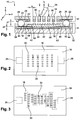
- a touch sensor 10 for example intended to be incorporated in a screen, a keyboard, or a touchpad, comprises a pressure sensor 12 and a light sensor 14. The latter is disposed under the pressure sensor 12 and the right thereof, the two sensors 12, 14 being electrically connected in parallel.
- the pressure sensor 12 comprises a piezoresistive layer 16, made of a piezoelectric material, whose electrical resistance varies as a function of the mechanical stresses that this material undergoes, sandwiched between protective layers, in particular a flexible substrate 18 defining a tactile surface, and an electrically insulating protective layer 20.
- the piezoresistive layer 16 is advantageously made of PEDOT: PSS, for example with a thickness of between 10 nm and 5 ⁇ m.
- the PEDOT: PSS is a piezoresistive material, that is to say a material whose electrical resistance varies greatly with the stresses it undergoes compared to other types of known piezoresistive materials.
- the PEDOT: PSS is also sensitive to temperature, and its electrical resistance decreases with increasing temperature.
- this material is substantially transparent to visible radiation and near infrared.
- Conductive elements 22 for example made of gold, platinum, nickel, copper, silver or aluminum, are furthermore made on the substrate 18 in contact with the piezoresistive layer 16, in order to subject it to ci to a voltage and / or inject in it an electric current, as will be explained in more detail later.
- the conductive elements 22 comprise two sets of metal tracks 24 in contact with the layer 16 and connected respectively to two metal pads 26.
- the flexible substrate 18 is selected deformable under the pressure exerted by an object on its surface, for example by a finger 28 or a stylus.
- the flexible substrate 18 is for example made of a thin plastic layer with a thickness of between 25 .mu.m and 200 .mu.m.
- the pressure sensor 12 is also designed at least partially transparent to the radiation detected by the light sensor 14.
- the transparency is obtained by the choice of the constituent materials of the sensor 12, and / or the thickness of the constituent layers of that and / or by arranging in the sensor preferred passages for the light, for example openings.
- the substrate 18 is made of a material at least partially transparent to visible light.
- the substrate 18 is made of polyethylene naphthalate (“PEN”) or poly (ethylene terephthalate) (“PET”), which has the triple advantage of being flexible, transparent to the visible spectrum and the near infrared, and to be inexpensive ..
- PEN polyethylene naphthalate
- PET poly (ethylene terephthalate)
- the protective layer 20 is preferably produced in a dielectric material which is at least partially transparent to the radiation detected by the sensor 14.
- the layer 20 is a CYTOP-type fluoropolymer layer, which is transparent and has a low permittivity, with a thickness of between 10 nanometers and 500 nanometers.
- Openings 30 are also made through the pressure sensor 12, and to the right of the light sensor 14, to increase the overall transparency of the sensor 12.
- a two-dimensional, particularly periodic, network of openings is produced through the substrate 18, the piezoresistive layer 16, and the protective layer 20.
- the openings are for example of square and side cross-section between 50 nanometers and 5 microns. micrometers.
- the piezoresistive layer 16 is made in the form of a solid rectangular layer traversed by the openings 30.
- the piezoresistive layer 20 alternatively takes the form of a coil running between rows of openings 30.
- a coil has a length much greater than its width, so that it is obtained an increased variation of its electrical resistance according to pressure exerted on its surface.
- the coil has more turns in a central zone of the pressure sensor 12 than at the periphery thereof. In this way, the pressure sensor is more sensitive on this central zone than on its periphery due to the low resonance frequency which gives a maximum of stress to the center of the piezoresistive structure.
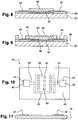
- the light sensor 14 comprises a substrate 32 on which a reflective layer 34 rests .
- the layer 34 is covered with a layer 36 of electrically insulating material and at least partially transparent to the radiation detected by the light sensor 14.
- Conductive elements 40 for example made of gold, platinum, nickel, copper, silver or aluminum, are also produced on the insulating layer 36 in contact with the photosensitive layer 38 to subject it to a voltage and / or inject therein an electric current, as will be explained in more detail later.
- the conductive elements 40 comprise two sets of metal tracks 42 in contact with the layer 38 and connected to two metal plates 44.
- the assembly is optionally covered with an electrically insulating protective layer 48, except for the conductive pads 44 which remain open, and openings 50 are made in the layer 48 to the right of the openings 30 of the pressure sensor 12.
- the substrate 32 is advantageously a flexible and transparent substrate, for example a plastic substrate, such as PEN or PET, with a thickness of between 25 ⁇ m and 200 ⁇ m.
- a plastic substrate such as PEN or PET
- the photosensitive layer 38 is advantageously constituted by a mixture of graphene and ATO (antimony doped tin dioxide (SnO 2: Sb)), the proportion by weight of ATO in the mixture is advantageously greater than 20%.
- ATO antimony doped tin dioxide
- Such a material is capable of capturing in the visible spectrum (especially in the red) as well as in the near infrared and furthermore has an electrical resistance which decreases as a function of the amount of radiation captured.
- the photosensitive layer 38 thus captures the ambient light variations induced by the presence of the finger 28, as well as the heat variations induced by the presence of the finger 28, these heat variations resulting in variations of the near-infrared radiation emitted by the finger .
- the reflecting layer 34 is made of a material having a significant reflection of the radiation detected by the photosensitive layer 38.
- the reflective layer is a metallic layer of silver, aluminum or gold, these materials having a high reflectivity in the field visible and near infrared.
- the insulating layer 36 consists of a material transparent to the radiation detected by the photosensitive layer 38, for example an organic polymer type dielectric or an inorganic oxide such as SiO 2 , ZrO 2 , TiO 2 , etc. . These materials have a high transparency in the visible and near infrared range.
- the pressure sensor 12 and the light sensor 14 are advantageously carried on one another by means of metal balls 52, each disposed between connection pads 26, 44 disposed facing the sensors 12, 14 respectively. .
- the sensors 12 and 14 are therefore electrically connected in parallel.
- the balls 52 spacing them a distance d 1 allowing the pressure sensor 12 to bend strongly under the pressure exerted on its surface, and therefore to undergo a large variation in its electrical resistance.
- the space between the pressure sensor 12 and the light sensor 14 is for example filled by a gas, such as air, under reduced pressure or not, vacuum, a fluid or viscous liquid, etc ...
- these two functions can be implemented by separate elements.
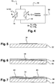
- the sensor 10 is for example connected to an electric circuit 54 comprising a source of current or constant voltage making it possible to measure the resistance of the resistor or of an electrical quantity connected thereto, this measurement being analyzed by a circuit of analog or digital processing (not shown) to determine an event on the surface of the sensor, such as the presence of a finger for example.
- an electric circuit 54 comprising a source of current or constant voltage making it possible to measure the resistance of the resistor or of an electrical quantity connected thereto, this measurement being analyzed by a circuit of analog or digital processing (not shown) to determine an event on the surface of the sensor, such as the presence of a finger for example.
- the sensor 10 thus combines three different detection modes, namely a piezoresistive tactile detection mode, a light detection mode, and a detection mode combining the tactile and light detection mode.
- the pressure exerted on the substrate 18 induces a piezoresistive effect, namely the variation of the electrical resistance of the piezoresistive layer 16 under the effect of the stress which it undergoes.
- the fact of pressing on the substrate 18 causes a local deformation of the piezoresistive layer 16, which causes a variation in its electrical resistance, a variation which results in a corresponding variation of an electrical quantity, in particular a current or a electric tension.
- the pressure exerted is then determined using, for example, a table of values of predetermined variations of the measured electrical quantity as a function of pressure values exerted.
- the light detection mode when a face, or both faces of the sensor 10 are illuminated, the electrical resistance of the photoresistor formed of the photosensitive layer 38 varies as a function of the light intensity, and the variation of this resistance is translated into an electrical magnitude, current or voltage, which is read by a read circuit in a manner similar to that described above.
- the light detection mode can also detect thermal waves in the near infrared, and thus allows the detection of a finger when the ambient light in the visible spectrum is of low intensity. It will also be noted that the materials and layers constituting the light sensor 14 allow detection of an incident light on the substrate 32, hence the possibility of detection only light if the application requires it.
- an object exerting a pressure on the surface of the pressure sensor 12 also masks the ambient luminosity and thus causes a light variation sensed by the light sensor 14.
- the object is a finger
- thermal waves in the near infrared can be further detected by the latter. The combination of these phenomena generates a large variation in the overall electrical resistance of the sensor, allowing a high sensitivity detection.
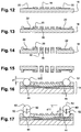
- the manufacture of the light sensor 14 begins with the production of a substrate 32 made of a flexible plastic bat cost of the PEN or PET type and with a thickness of between 25 and 200 micrometers, and continues with the deposition of a reflective metal layer. 34, for example silver, aluminum or gold, by means of a physical vapor deposition, a screen printing or an inkjet printing ( figure 5 ).
- An electrically insulating and transparent layer 36 is then deposited, for example by means of a physical vapor deposition, a screen printing or an inkjet printing, on the assembly obtained.
- the thickness of the layer 36 is chosen so as to maximize the reflection of the luminous flux on the photosensitive element, which will subsequently be deposited ( figure 6 ).
- the constituent material of the layer 36 is, for example, an organic polymer type dielectric or an inorganic passivation oxide such as SiO 2 , ZrO 2 , TiO 2 , or others.
- connection electrodes 40 are then made on the layer 36 by means of a physical vapor deposition, a screen printing or an inkjet printing ( figure 7 ).
- the electrodes 40 are for example made of conductive graphene or a metal, especially gold, silver, aluminum, platinum, copper, or titanium.
- the process is continued by the deposition of the photosensitive layer 38 consisting of a mixture of graphene and ATO with a minimum of 20% by weight of ATO ( figure 8 ).
- the deposition is carried out for example by means of a screen printing or an inkjet printing depositing a mixture of a conductive graphene ink and an ATO ink.
- the solvents of the graphene ink and the ATO ink advantageously have an evaporation temperature close to each other to form a very uniform deposited layer.
- the evaporation temperatures of the solvents are also advantageously chosen, compatible in terms of annealing, with a annealing temperature of the layers already formed during the deposition of the ink mixture, and in particular the evaporation temperatures below the glass transition temperature. of the plastic substrate 32.
- the evaporation temperatures are between 110 and 180 ° C.
- a dielectric layer 48 is then deposited on the assembly, for example by means of a physical vapor deposition, a screen printing or an inkjet printing, and openings 50 are made in the layer 48. up to the photoresist layer 38 ( Figures 9 and 10 ).
- the openings are for example made by means of screen printing or lithography.
- the manufacture of the pressure sensor 12 begins with the realization of a substrate 18 made of flexible plastic bat cost type PEN or PET, a thickness of between 25 and 200 micrometers, and continues with the realization of two electrodes 22, in particular by means of a full-plate deposit, for example a physical vapor deposition or by screen printing or by ink-jet printing, followed by a chemical, physical or laser etching, in order to define the electrodes 22 ( figure 11 ).
- the electrodes 22 consist for example of conductive graphene or a metal, especially gold, silver, aluminum, platinum, copper, or titanium.
- a piezoresistive layer 16 advantageously consisting of PEDOT: PSS, is deposited on the substrate 18 and partially on the two electrodes 22, for example by screen printing or by inkjet printing.
- the geometric shape of the piezoresistive layer 16 is advantageously chosen to increase the sensitivity of the pressure sensor 12 in the center thereof by defining the serpentine pattern with tight turns in the center of the sensor ( figure 12 ).
- the layer 20 is for example deposited by screen printing or by inkjet printing, and more generally by means of a low temperature deposition compatible with the plastic substrate 18. An annealing is then applied to stiffen the layer 20.
- Openings 30 are then made in the substrate 18, for example by means of laser etching, plasma etching, or chemical etching, through a lithography mask ( figure 14 ).
- the dimensions of the openings 30 in the thickness of the substrate 18, and therefore through the pressure sensor 12, are advantageously optimized to have a maximum of light transfer to the light sensor 14.
- the dimensions of the openings are chosen to limit or avoid diffraction phenomena by the layers forming the pressure sensor 12 for the wavelengths detected by the light sensor 14.
- the pressure and light sensors 12 and 14 are completed, they are preferably assembled using a conductive ink, for example based on silver.
- a drop of a conductive ink of the epoxy or other type comprising silver is deposited on each of the connection pads 44 of the light sensor 12, for example by screen printing or by means of a micro-syringe.
- the ink volume and the deposition conditions thereof make it possible to adjust the distance d 1 separating the pressure sensor 12 from the light sensor 14 ( figure 16 ).
- Light annealing is then performed to solidify the surface of the ink drops and then the pressure sensor 12 is then transferred to the conductive balls 52.
- a final annealing is then applied to solidify all the conductive balls.
- a first drop of conductive ink 52 is deposited on each connection pad 44, then a superficial annealing of the drops is applied in order to solidify their upper surfaces.
- a rigid metal insert 60 conductive, and having high adhesion properties with the conductive ink, is then inserted into each of the drops to mechanically support the structure of the final sensor and to prevent fatigue thereof following multiple tactile touch that it will undergo.
- the inserts 60 are rods of conductive carbon nanotubes, tungsten, nickel, titanium nitride, or tungsten nitride.
- a second drop 62 is then deposited on each of the first drops 52, and annealing is applied to stiffen the assembly.
- photosensitive layer consisting of a mixture of graphene and ATO has been described.
- Other photosensitive materials are also possible.
Landscapes
- Engineering & Computer Science (AREA)
- Physics & Mathematics (AREA)
- General Physics & Mathematics (AREA)
- General Engineering & Computer Science (AREA)
- Theoretical Computer Science (AREA)
- Spectroscopy & Molecular Physics (AREA)
- Human Computer Interaction (AREA)
- Force Measurement Appropriate To Specific Purposes (AREA)
Applications Claiming Priority (2)
| Application Number | Priority Date | Filing Date | Title |
|---|---|---|---|
| FR1253649A FR2989829B1 (fr) | 2012-04-20 | 2012-04-20 | Capteur tactile photosensible |
| PCT/FR2013/050672 WO2013156702A1 (fr) | 2012-04-20 | 2013-03-28 | Capteur tactile photosensible |
Publications (2)
| Publication Number | Publication Date |
|---|---|
| EP2839361A1 EP2839361A1 (fr) | 2015-02-25 |
| EP2839361B1 true EP2839361B1 (fr) | 2016-03-23 |
Family
ID=48237092
Family Applications (1)
| Application Number | Title | Priority Date | Filing Date |
|---|---|---|---|
| EP13719938.6A Not-in-force EP2839361B1 (fr) | 2012-04-20 | 2013-03-28 | Capteur tactile photosensible |
Country Status (6)
| Country | Link |
|---|---|
| US (1) | US9228908B2 (enExample) |
| EP (1) | EP2839361B1 (enExample) |
| JP (1) | JP6125611B2 (enExample) |
| KR (1) | KR20140146594A (enExample) |
| FR (1) | FR2989829B1 (enExample) |
| WO (1) | WO2013156702A1 (enExample) |
Families Citing this family (12)
| Publication number | Priority date | Publication date | Assignee | Title |
|---|---|---|---|---|
| FR2989677B1 (fr) * | 2012-04-20 | 2015-06-19 | Commissariat Energie Atomique | Materiau photosensible et thermoresistant, procede de preparation et utilisation |
| FR3032042B1 (fr) * | 2015-01-23 | 2018-03-02 | Commissariat A L'energie Atomique Et Aux Energies Alternatives | Dispositif d'acquisition d'une image caracteristique d'un corps |
| US10416031B2 (en) * | 2015-09-25 | 2019-09-17 | MedicusTek, Inc. | Pressure sensing device |
| KR102381652B1 (ko) * | 2015-09-30 | 2022-04-04 | 삼성디스플레이 주식회사 | 표시장치 |
| CN106059557A (zh) * | 2016-06-01 | 2016-10-26 | 郭利民 | 一种采用光敏元件的键及使用该键的键盘 |
| CN106445239B (zh) * | 2016-10-31 | 2019-11-12 | 厦门天马微电子有限公司 | 一种触控显示装置、触控显示面板及其压力检测方法 |
| US11054932B2 (en) * | 2017-09-06 | 2021-07-06 | Apple Inc. | Electronic device having a touch sensor, force sensor, and haptic actuator in an integrated module |
| US11552240B2 (en) * | 2017-10-24 | 2023-01-10 | Purdue Research Foundation | Machines and processes for producing polymer films and films produced thereby |
| CN108871592B (zh) * | 2018-05-08 | 2020-07-03 | 电子科技大学 | 一种低压电及温度干扰的柔性热释电红外热像仪像素阵列 |
| US10794786B2 (en) | 2018-09-24 | 2020-10-06 | Honeywell International Inc. | Miniature size force sensor with bubble detection capabilities |
| US10966007B1 (en) | 2018-09-25 | 2021-03-30 | Apple Inc. | Haptic output system |
| US11024135B1 (en) | 2020-06-17 | 2021-06-01 | Apple Inc. | Portable electronic device having a haptic button assembly |
Family Cites Families (24)
| Publication number | Priority date | Publication date | Assignee | Title |
|---|---|---|---|---|
| JPH06332607A (ja) * | 1993-05-19 | 1994-12-02 | Mitsubishi Electric Corp | 表示一体型入力装置 |
| JPH10249768A (ja) * | 1997-03-12 | 1998-09-22 | Tokai Rubber Ind Ltd | 力センサー |
| US6522032B1 (en) * | 1999-05-07 | 2003-02-18 | Easter-Owen Electric Company | Electrical switch and method of generating an electrical switch output signal |
| US6909084B2 (en) * | 2000-08-31 | 2005-06-21 | Toudai Tlo, Ltd | Optical tactile sensor having a transparent elastic tactile portion |
| JP2004127073A (ja) * | 2002-10-04 | 2004-04-22 | Smk Corp | 指示入力装置 |
| JP2004139162A (ja) * | 2002-10-15 | 2004-05-13 | Fujitsu Component Ltd | タッチパネルの製造方法と、該製造方法で製造されるタッチパネル |
| JP2006013407A (ja) * | 2004-05-21 | 2006-01-12 | Sanyo Electric Co Ltd | 光量検出回路およびそれを用いた表示パネル |
| JP2006048548A (ja) * | 2004-08-06 | 2006-02-16 | Citizen Seimitsu Co Ltd | タッチパネル |
| KR101365491B1 (ko) * | 2006-11-17 | 2014-02-24 | 삼성디스플레이 주식회사 | 디스플레이장치 |
| JP4450089B2 (ja) * | 2007-10-12 | 2010-04-14 | エプソンイメージングデバイス株式会社 | タッチパネル及び電気光学装置 |
| WO2009055767A2 (en) * | 2007-10-26 | 2009-04-30 | Trs Technologies, Inc. | Micromachined piezoelectric ultrasound transducer arrays |
| JP5399799B2 (ja) * | 2008-07-17 | 2014-01-29 | 三星ディスプレイ株式會社 | ディスプレイ装置 |
| US20100123686A1 (en) * | 2008-11-19 | 2010-05-20 | Sony Ericsson Mobile Communications Ab | Piezoresistive force sensor integrated in a display |
| TWI376624B (en) * | 2008-12-23 | 2012-11-11 | Integrated Digital Tech Inc | Force-sensing modules for light sensitive screens |
| JP5100670B2 (ja) * | 2009-01-21 | 2012-12-19 | 株式会社半導体エネルギー研究所 | タッチパネル、電子機器 |
| AT508438B1 (de) * | 2009-04-16 | 2013-10-15 | Isiqiri Interface Tech Gmbh | Anzeigefläche und eine damit kombinierte steuervorrichtung für eine datenverarbeitungsanlage |
| US8981213B1 (en) * | 2009-05-20 | 2015-03-17 | Joseph A. Micallef | Piezoelectric ultracapacitive photovoltaic cell |
| TW201203052A (en) * | 2010-05-03 | 2012-01-16 | Flatfrog Lab Ab | Touch determination by tomographic reconstruction |
| SG186204A1 (en) * | 2010-06-11 | 2013-01-30 | 3M Innovative Properties Co | Positional touch sensor with force measurement |
| US9417141B2 (en) * | 2011-09-16 | 2016-08-16 | Sony Corporation | Force sensitive touch sensor |
| TW201317839A (zh) * | 2011-10-25 | 2013-05-01 | Au Optronics Corp | 觸控筆、觸控顯示系統以及觸控顯示方法 |
| US9823781B2 (en) * | 2011-12-06 | 2017-11-21 | Nri R&D Patent Licensing, Llc | Heterogeneous tactile sensing via multiple sensor types |
| US9465439B2 (en) * | 2012-01-13 | 2016-10-11 | Kyocera Corporation | Electronic device and control method of electronic device |
| US8526770B2 (en) * | 2012-01-30 | 2013-09-03 | Empire Technology Development Llc | Systems, materials, and methods for a mechanical stress activated interface using piezo-optical components |
-
2012
- 2012-04-20 FR FR1253649A patent/FR2989829B1/fr not_active Expired - Fee Related
-
2013
- 2013-03-28 EP EP13719938.6A patent/EP2839361B1/fr not_active Not-in-force
- 2013-03-28 JP JP2015506279A patent/JP6125611B2/ja active Active
- 2013-03-28 KR KR1020147027051A patent/KR20140146594A/ko not_active Withdrawn
- 2013-03-28 US US14/388,536 patent/US9228908B2/en not_active Expired - Fee Related
- 2013-03-28 WO PCT/FR2013/050672 patent/WO2013156702A1/fr not_active Ceased
Also Published As
| Publication number | Publication date |
|---|---|
| EP2839361A1 (fr) | 2015-02-25 |
| FR2989829B1 (fr) | 2014-04-11 |
| US9228908B2 (en) | 2016-01-05 |
| JP2015515067A (ja) | 2015-05-21 |
| FR2989829A1 (fr) | 2013-10-25 |
| KR20140146594A (ko) | 2014-12-26 |
| WO2013156702A1 (fr) | 2013-10-24 |
| US20150049330A1 (en) | 2015-02-19 |
| JP6125611B2 (ja) | 2017-05-10 |
Similar Documents
| Publication | Publication Date | Title |
|---|---|---|
| EP2839361B1 (fr) | Capteur tactile photosensible | |
| EP2756278B1 (fr) | Capteur de pression piezoelectrique | |
| EP2385486B1 (fr) | Transducteur de variation temporelle de température,puce électronique incorporant ce transducteur et procédé de fabrication de cette puce | |
| EP2836896B1 (fr) | Capteur tactile et procede de fabrication d'un tel capteur | |
| EP2602598B1 (fr) | Détecteur bolométrique d'un rayonnement électromagnetique dans le domaine du térahertz et dispositif de détection matriciel comportant de tels détecteurs | |
| EP1614023B8 (fr) | Dispositif de détection de position | |
| EP2836895B1 (fr) | Dispositif d'interface utilisateur a electrodes transparentes | |
| EP2800957B1 (fr) | Capteur de temperature capacitif comprenant deux condensateurs en pont diviseur de tension | |
| EP1715315A1 (fr) | Détecteur bolométrique, dispositif de détection d'ondes électromagnétiques submillimétriques et millimétriques mettant en oeuvre un tel détecteur | |
| EP3775817A1 (fr) | Capteur et écran tactile à compensation environnementale, notamment en température | |
| EP2019301B1 (fr) | Détecteur de rayonnement électromagnétique et procédé de fabrication d'un tel détecteur | |
| EP3483787A1 (fr) | Procédé de réalisation d'un empilement de couches pour un capteur thermique matriciel | |
| FR2958748A1 (fr) | Dispositif formant capteur de pression, procede de realisation d'un tel capteur et application a la realisation d'un ecran tactile | |
| EP3435285B1 (fr) | Capteur thermique avec deux portions pyroélectriques superposées, pour la mesure d'un différentiel de charges | |
| WO2023111344A1 (fr) | Microcapteur à électrodes interdigitées | |
| EP3640615B1 (fr) | Capteur pyroelectrique avec revêtement amélioré de résistance contre l'abrasion | |
| WO2012069771A1 (fr) | Capteur tactile et procédé de fabrication associe | |
| FR3034248A1 (fr) | Dispositif a resistance thermosensible | |
| WO2024213465A1 (fr) | Dispositif piezoelectrique flexible de mesure de deformation, unidirectionnel, bidirectionel ou omnidirectionnel | |
| EP2385485B1 (fr) | Procédé de calibration d'une puce électronique et détecteur de motif thermique pour ce procédé | |
| EP3502638A1 (fr) | Capteur pyroelectrique avec blindage électro-magnétique comprenant un matériau composite | |
| EP3757735B1 (fr) | Dispositif a surface tactile | |
| EP3846209A1 (fr) | Composant de détection incluant des pixels noirs et procédé de fabrication d'un tel composant | |
| WO2018042115A1 (fr) | Capteur de motifs thermiques par imagerie infrarouge d'une matrice d'éléments chauffants. |
Legal Events
| Date | Code | Title | Description |
|---|---|---|---|
| PUAI | Public reference made under article 153(3) epc to a published international application that has entered the european phase |
Free format text: ORIGINAL CODE: 0009012 |
|
| 17P | Request for examination filed |
Effective date: 20140929 |
|
| AK | Designated contracting states |
Kind code of ref document: A1 Designated state(s): AL AT BE BG CH CY CZ DE DK EE ES FI FR GB GR HR HU IE IS IT LI LT LU LV MC MK MT NL NO PL PT RO RS SE SI SK SM TR |
|
| AX | Request for extension of the european patent |
Extension state: BA ME |
|
| DAX | Request for extension of the european patent (deleted) | ||
| GRAP | Despatch of communication of intention to grant a patent |
Free format text: ORIGINAL CODE: EPIDOSNIGR1 |
|
| INTG | Intention to grant announced |
Effective date: 20151217 |
|
| INTG | Intention to grant announced |
Effective date: 20151222 |
|
| GRAS | Grant fee paid |
Free format text: ORIGINAL CODE: EPIDOSNIGR3 |
|
| GRAA | (expected) grant |
Free format text: ORIGINAL CODE: 0009210 |
|
| AK | Designated contracting states |
Kind code of ref document: B1 Designated state(s): AL AT BE BG CH CY CZ DE DK EE ES FI FR GB GR HR HU IE IS IT LI LT LU LV MC MK MT NL NO PL PT RO RS SE SI SK SM TR |
|
| REG | Reference to a national code |
Ref country code: GB Ref legal event code: FG4D Free format text: NOT ENGLISH |
|
| REG | Reference to a national code |
Ref country code: CH Ref legal event code: EP Ref country code: FR Ref legal event code: PLFP Year of fee payment: 4 |
|
| REG | Reference to a national code |
Ref country code: AT Ref legal event code: REF Ref document number: 783756 Country of ref document: AT Kind code of ref document: T Effective date: 20160415 |
|
| REG | Reference to a national code |
Ref country code: IE Ref legal event code: FG4D Free format text: LANGUAGE OF EP DOCUMENT: FRENCH |
|
| REG | Reference to a national code |
Ref country code: DE Ref legal event code: R096 Ref document number: 602013005738 Country of ref document: DE |
|
| REG | Reference to a national code |
Ref country code: LT Ref legal event code: MG4D |
|
| REG | Reference to a national code |
Ref country code: NL Ref legal event code: MP Effective date: 20160323 |
|
| PG25 | Lapsed in a contracting state [announced via postgrant information from national office to epo] |
Ref country code: GR Free format text: LAPSE BECAUSE OF FAILURE TO SUBMIT A TRANSLATION OF THE DESCRIPTION OR TO PAY THE FEE WITHIN THE PRESCRIBED TIME-LIMIT Effective date: 20160624 Ref country code: HR Free format text: LAPSE BECAUSE OF FAILURE TO SUBMIT A TRANSLATION OF THE DESCRIPTION OR TO PAY THE FEE WITHIN THE PRESCRIBED TIME-LIMIT Effective date: 20160323 Ref country code: NO Free format text: LAPSE BECAUSE OF FAILURE TO SUBMIT A TRANSLATION OF THE DESCRIPTION OR TO PAY THE FEE WITHIN THE PRESCRIBED TIME-LIMIT Effective date: 20160623 Ref country code: FI Free format text: LAPSE BECAUSE OF FAILURE TO SUBMIT A TRANSLATION OF THE DESCRIPTION OR TO PAY THE FEE WITHIN THE PRESCRIBED TIME-LIMIT Effective date: 20160323 |
|
| REG | Reference to a national code |
Ref country code: AT Ref legal event code: MK05 Ref document number: 783756 Country of ref document: AT Kind code of ref document: T Effective date: 20160323 |
|
| PG25 | Lapsed in a contracting state [announced via postgrant information from national office to epo] |
Ref country code: SE Free format text: LAPSE BECAUSE OF FAILURE TO SUBMIT A TRANSLATION OF THE DESCRIPTION OR TO PAY THE FEE WITHIN THE PRESCRIBED TIME-LIMIT Effective date: 20160323 Ref country code: BE Free format text: LAPSE BECAUSE OF NON-PAYMENT OF DUE FEES Effective date: 20160331 Ref country code: NL Free format text: LAPSE BECAUSE OF FAILURE TO SUBMIT A TRANSLATION OF THE DESCRIPTION OR TO PAY THE FEE WITHIN THE PRESCRIBED TIME-LIMIT Effective date: 20160323 Ref country code: RS Free format text: LAPSE BECAUSE OF FAILURE TO SUBMIT A TRANSLATION OF THE DESCRIPTION OR TO PAY THE FEE WITHIN THE PRESCRIBED TIME-LIMIT Effective date: 20160323 Ref country code: LV Free format text: LAPSE BECAUSE OF FAILURE TO SUBMIT A TRANSLATION OF THE DESCRIPTION OR TO PAY THE FEE WITHIN THE PRESCRIBED TIME-LIMIT Effective date: 20160323 Ref country code: LT Free format text: LAPSE BECAUSE OF FAILURE TO SUBMIT A TRANSLATION OF THE DESCRIPTION OR TO PAY THE FEE WITHIN THE PRESCRIBED TIME-LIMIT Effective date: 20160323 |
|
| PG25 | Lapsed in a contracting state [announced via postgrant information from national office to epo] |
Ref country code: IS Free format text: LAPSE BECAUSE OF FAILURE TO SUBMIT A TRANSLATION OF THE DESCRIPTION OR TO PAY THE FEE WITHIN THE PRESCRIBED TIME-LIMIT Effective date: 20160723 Ref country code: PL Free format text: LAPSE BECAUSE OF FAILURE TO SUBMIT A TRANSLATION OF THE DESCRIPTION OR TO PAY THE FEE WITHIN THE PRESCRIBED TIME-LIMIT Effective date: 20160323 Ref country code: EE Free format text: LAPSE BECAUSE OF FAILURE TO SUBMIT A TRANSLATION OF THE DESCRIPTION OR TO PAY THE FEE WITHIN THE PRESCRIBED TIME-LIMIT Effective date: 20160323 |
|
| REG | Reference to a national code |
Ref country code: CH Ref legal event code: PL |
|
| PG25 | Lapsed in a contracting state [announced via postgrant information from national office to epo] |
Ref country code: RO Free format text: LAPSE BECAUSE OF FAILURE TO SUBMIT A TRANSLATION OF THE DESCRIPTION OR TO PAY THE FEE WITHIN THE PRESCRIBED TIME-LIMIT Effective date: 20160323 Ref country code: ES Free format text: LAPSE BECAUSE OF FAILURE TO SUBMIT A TRANSLATION OF THE DESCRIPTION OR TO PAY THE FEE WITHIN THE PRESCRIBED TIME-LIMIT Effective date: 20160323 Ref country code: CZ Free format text: LAPSE BECAUSE OF FAILURE TO SUBMIT A TRANSLATION OF THE DESCRIPTION OR TO PAY THE FEE WITHIN THE PRESCRIBED TIME-LIMIT Effective date: 20160323 Ref country code: AT Free format text: LAPSE BECAUSE OF FAILURE TO SUBMIT A TRANSLATION OF THE DESCRIPTION OR TO PAY THE FEE WITHIN THE PRESCRIBED TIME-LIMIT Effective date: 20160323 Ref country code: SM Free format text: LAPSE BECAUSE OF FAILURE TO SUBMIT A TRANSLATION OF THE DESCRIPTION OR TO PAY THE FEE WITHIN THE PRESCRIBED TIME-LIMIT Effective date: 20160323 Ref country code: SK Free format text: LAPSE BECAUSE OF FAILURE TO SUBMIT A TRANSLATION OF THE DESCRIPTION OR TO PAY THE FEE WITHIN THE PRESCRIBED TIME-LIMIT Effective date: 20160323 Ref country code: PT Free format text: LAPSE BECAUSE OF FAILURE TO SUBMIT A TRANSLATION OF THE DESCRIPTION OR TO PAY THE FEE WITHIN THE PRESCRIBED TIME-LIMIT Effective date: 20160725 |
|
| REG | Reference to a national code |
Ref country code: IE Ref legal event code: MM4A |
|
| PG25 | Lapsed in a contracting state [announced via postgrant information from national office to epo] |
Ref country code: IT Free format text: LAPSE BECAUSE OF FAILURE TO SUBMIT A TRANSLATION OF THE DESCRIPTION OR TO PAY THE FEE WITHIN THE PRESCRIBED TIME-LIMIT Effective date: 20160323 |
|
| REG | Reference to a national code |
Ref country code: DE Ref legal event code: R097 Ref document number: 602013005738 Country of ref document: DE |
|
| PLBE | No opposition filed within time limit |
Free format text: ORIGINAL CODE: 0009261 |
|
| STAA | Information on the status of an ep patent application or granted ep patent |
Free format text: STATUS: NO OPPOSITION FILED WITHIN TIME LIMIT |
|
| PG25 | Lapsed in a contracting state [announced via postgrant information from national office to epo] |
Ref country code: IE Free format text: LAPSE BECAUSE OF NON-PAYMENT OF DUE FEES Effective date: 20160328 Ref country code: DK Free format text: LAPSE BECAUSE OF FAILURE TO SUBMIT A TRANSLATION OF THE DESCRIPTION OR TO PAY THE FEE WITHIN THE PRESCRIBED TIME-LIMIT Effective date: 20160323 Ref country code: CH Free format text: LAPSE BECAUSE OF NON-PAYMENT OF DUE FEES Effective date: 20160331 Ref country code: LI Free format text: LAPSE BECAUSE OF NON-PAYMENT OF DUE FEES Effective date: 20160331 |
|
| PG25 | Lapsed in a contracting state [announced via postgrant information from national office to epo] |
Ref country code: BG Free format text: LAPSE BECAUSE OF FAILURE TO SUBMIT A TRANSLATION OF THE DESCRIPTION OR TO PAY THE FEE WITHIN THE PRESCRIBED TIME-LIMIT Effective date: 20160623 |
|
| 26N | No opposition filed |
Effective date: 20170102 |
|
| REG | Reference to a national code |
Ref country code: FR Ref legal event code: PLFP Year of fee payment: 5 |
|
| PG25 | Lapsed in a contracting state [announced via postgrant information from national office to epo] |
Ref country code: SI Free format text: LAPSE BECAUSE OF FAILURE TO SUBMIT A TRANSLATION OF THE DESCRIPTION OR TO PAY THE FEE WITHIN THE PRESCRIBED TIME-LIMIT Effective date: 20160323 |
|
| PG25 | Lapsed in a contracting state [announced via postgrant information from national office to epo] |
Ref country code: MT Free format text: LAPSE BECAUSE OF FAILURE TO SUBMIT A TRANSLATION OF THE DESCRIPTION OR TO PAY THE FEE WITHIN THE PRESCRIBED TIME-LIMIT Effective date: 20160323 |
|
| REG | Reference to a national code |
Ref country code: FR Ref legal event code: PLFP Year of fee payment: 6 |
|
| PG25 | Lapsed in a contracting state [announced via postgrant information from national office to epo] |
Ref country code: HU Free format text: LAPSE BECAUSE OF FAILURE TO SUBMIT A TRANSLATION OF THE DESCRIPTION OR TO PAY THE FEE WITHIN THE PRESCRIBED TIME-LIMIT; INVALID AB INITIO Effective date: 20130328 |
|
| PG25 | Lapsed in a contracting state [announced via postgrant information from national office to epo] |
Ref country code: LU Free format text: LAPSE BECAUSE OF NON-PAYMENT OF DUE FEES Effective date: 20160328 Ref country code: MK Free format text: LAPSE BECAUSE OF FAILURE TO SUBMIT A TRANSLATION OF THE DESCRIPTION OR TO PAY THE FEE WITHIN THE PRESCRIBED TIME-LIMIT Effective date: 20160323 Ref country code: CY Free format text: LAPSE BECAUSE OF FAILURE TO SUBMIT A TRANSLATION OF THE DESCRIPTION OR TO PAY THE FEE WITHIN THE PRESCRIBED TIME-LIMIT Effective date: 20160323 Ref country code: MC Free format text: LAPSE BECAUSE OF FAILURE TO SUBMIT A TRANSLATION OF THE DESCRIPTION OR TO PAY THE FEE WITHIN THE PRESCRIBED TIME-LIMIT Effective date: 20160323 |
|
| PG25 | Lapsed in a contracting state [announced via postgrant information from national office to epo] |
Ref country code: TR Free format text: LAPSE BECAUSE OF FAILURE TO SUBMIT A TRANSLATION OF THE DESCRIPTION OR TO PAY THE FEE WITHIN THE PRESCRIBED TIME-LIMIT Effective date: 20160323 Ref country code: AL Free format text: LAPSE BECAUSE OF FAILURE TO SUBMIT A TRANSLATION OF THE DESCRIPTION OR TO PAY THE FEE WITHIN THE PRESCRIBED TIME-LIMIT Effective date: 20160323 |
|
| PGFP | Annual fee paid to national office [announced via postgrant information from national office to epo] |
Ref country code: FR Payment date: 20210330 Year of fee payment: 9 |
|
| PGFP | Annual fee paid to national office [announced via postgrant information from national office to epo] |
Ref country code: DE Payment date: 20210310 Year of fee payment: 9 Ref country code: GB Payment date: 20210318 Year of fee payment: 9 |
|
| REG | Reference to a national code |
Ref country code: DE Ref legal event code: R119 Ref document number: 602013005738 Country of ref document: DE |
|
| GBPC | Gb: european patent ceased through non-payment of renewal fee |
Effective date: 20220328 |
|
| PG25 | Lapsed in a contracting state [announced via postgrant information from national office to epo] |
Ref country code: GB Free format text: LAPSE BECAUSE OF NON-PAYMENT OF DUE FEES Effective date: 20220328 Ref country code: FR Free format text: LAPSE BECAUSE OF NON-PAYMENT OF DUE FEES Effective date: 20220331 Ref country code: DE Free format text: LAPSE BECAUSE OF NON-PAYMENT OF DUE FEES Effective date: 20221001 |