EP2838046A1 - Antenna circuit - Google Patents
Antenna circuit Download PDFInfo
- Publication number
- EP2838046A1 EP2838046A1 EP14180359.3A EP14180359A EP2838046A1 EP 2838046 A1 EP2838046 A1 EP 2838046A1 EP 14180359 A EP14180359 A EP 14180359A EP 2838046 A1 EP2838046 A1 EP 2838046A1
- Authority
- EP
- European Patent Office
- Prior art keywords
- antenna coil
- electrically conductive
- conductive layer
- antenna
- electrically
- Prior art date
- Legal status (The legal status is an assumption and is not a legal conclusion. Google has not performed a legal analysis and makes no representation as to the accuracy of the status listed.)
- Withdrawn
Links
Images
Classifications
-
- G—PHYSICS
- G06—COMPUTING OR CALCULATING; COUNTING
- G06K—GRAPHICAL DATA READING; PRESENTATION OF DATA; RECORD CARRIERS; HANDLING RECORD CARRIERS
- G06K7/00—Methods or arrangements for sensing record carriers, e.g. for reading patterns
- G06K7/10—Methods or arrangements for sensing record carriers, e.g. for reading patterns by electromagnetic radiation, e.g. optical sensing; by corpuscular radiation
- G06K7/10009—Methods or arrangements for sensing record carriers, e.g. for reading patterns by electromagnetic radiation, e.g. optical sensing; by corpuscular radiation sensing by radiation using wavelengths larger than 0.1 mm, e.g. radio-waves or microwaves
- G06K7/10316—Methods or arrangements for sensing record carriers, e.g. for reading patterns by electromagnetic radiation, e.g. optical sensing; by corpuscular radiation sensing by radiation using wavelengths larger than 0.1 mm, e.g. radio-waves or microwaves using at least one antenna particularly designed for interrogating the wireless record carriers
- G06K7/10336—Methods or arrangements for sensing record carriers, e.g. for reading patterns by electromagnetic radiation, e.g. optical sensing; by corpuscular radiation sensing by radiation using wavelengths larger than 0.1 mm, e.g. radio-waves or microwaves using at least one antenna particularly designed for interrogating the wireless record carriers the antenna being of the near field type, inductive coil
-
- H—ELECTRICITY
- H01—ELECTRIC ELEMENTS
- H01Q—ANTENNAS, i.e. RADIO AERIALS
- H01Q1/00—Details of, or arrangements associated with, antennas
- H01Q1/12—Supports; Mounting means
- H01Q1/22—Supports; Mounting means by structural association with other equipment or articles
- H01Q1/2208—Supports; Mounting means by structural association with other equipment or articles associated with components used in interrogation type services, i.e. in systems for information exchange between an interrogator/reader and a tag/transponder, e.g. in Radio Frequency Identification [RFID] systems
- H01Q1/2216—Supports; Mounting means by structural association with other equipment or articles associated with components used in interrogation type services, i.e. in systems for information exchange between an interrogator/reader and a tag/transponder, e.g. in Radio Frequency Identification [RFID] systems used in interrogator/reader equipment
-
- H—ELECTRICITY
- H01—ELECTRIC ELEMENTS
- H01Q—ANTENNAS, i.e. RADIO AERIALS
- H01Q1/00—Details of, or arrangements associated with, antennas
- H01Q1/12—Supports; Mounting means
- H01Q1/22—Supports; Mounting means by structural association with other equipment or articles
- H01Q1/2208—Supports; Mounting means by structural association with other equipment or articles associated with components used in interrogation type services, i.e. in systems for information exchange between an interrogator/reader and a tag/transponder, e.g. in Radio Frequency Identification [RFID] systems
- H01Q1/2225—Supports; Mounting means by structural association with other equipment or articles associated with components used in interrogation type services, i.e. in systems for information exchange between an interrogator/reader and a tag/transponder, e.g. in Radio Frequency Identification [RFID] systems used in active tags, i.e. provided with its own power source or in passive tags, i.e. deriving power from RF signal
-
- H—ELECTRICITY
- H01—ELECTRIC ELEMENTS
- H01Q—ANTENNAS, i.e. RADIO AERIALS
- H01Q7/00—Loop antennas with a substantially uniform current distribution around the loop and having a directional radiation pattern in a plane perpendicular to the plane of the loop
-
- H—ELECTRICITY
- H04—ELECTRIC COMMUNICATION TECHNIQUE
- H04B—TRANSMISSION
- H04B5/00—Near-field transmission systems, e.g. inductive or capacitive transmission systems
- H04B5/40—Near-field transmission systems, e.g. inductive or capacitive transmission systems characterised by components specially adapted for near-field transmission
- H04B5/43—Antennas
-
- G—PHYSICS
- G06—COMPUTING OR CALCULATING; COUNTING
- G06K—GRAPHICAL DATA READING; PRESENTATION OF DATA; RECORD CARRIERS; HANDLING RECORD CARRIERS
- G06K19/00—Record carriers for use with machines and with at least a part designed to carry digital markings
- G06K19/06—Record carriers for use with machines and with at least a part designed to carry digital markings characterised by the kind of the digital marking, e.g. shape, nature, code
- G06K19/067—Record carriers with conductive marks, printed circuits or semiconductor circuit elements, e.g. credit or identity cards also with resonating or responding marks without active components
- G06K19/07—Record carriers with conductive marks, printed circuits or semiconductor circuit elements, e.g. credit or identity cards also with resonating or responding marks without active components with integrated circuit chips
- G06K19/077—Constructional details, e.g. mounting of circuits in the carrier
- G06K19/07749—Constructional details, e.g. mounting of circuits in the carrier the record carrier being capable of non-contact communication, e.g. constructional details of the antenna of a non-contact smart card
- G06K19/07773—Antenna details
- G06K19/07777—Antenna details the antenna being of the inductive type
- G06K19/07779—Antenna details the antenna being of the inductive type the inductive antenna being a coil
- G06K19/07783—Antenna details the antenna being of the inductive type the inductive antenna being a coil the coil being planar
-
- G—PHYSICS
- G06—COMPUTING OR CALCULATING; COUNTING
- G06K—GRAPHICAL DATA READING; PRESENTATION OF DATA; RECORD CARRIERS; HANDLING RECORD CARRIERS
- G06K7/00—Methods or arrangements for sensing record carriers, e.g. for reading patterns
- G06K7/10—Methods or arrangements for sensing record carriers, e.g. for reading patterns by electromagnetic radiation, e.g. optical sensing; by corpuscular radiation
- G06K2007/10524—Hand-held scanners
-
- G—PHYSICS
- G06—COMPUTING OR CALCULATING; COUNTING
- G06K—GRAPHICAL DATA READING; PRESENTATION OF DATA; RECORD CARRIERS; HANDLING RECORD CARRIERS
- G06K7/00—Methods or arrangements for sensing record carriers, e.g. for reading patterns
- G06K7/10—Methods or arrangements for sensing record carriers, e.g. for reading patterns by electromagnetic radiation, e.g. optical sensing; by corpuscular radiation
- G06K7/10009—Methods or arrangements for sensing record carriers, e.g. for reading patterns by electromagnetic radiation, e.g. optical sensing; by corpuscular radiation sensing by radiation using wavelengths larger than 0.1 mm, e.g. radio-waves or microwaves
- G06K7/10366—Methods or arrangements for sensing record carriers, e.g. for reading patterns by electromagnetic radiation, e.g. optical sensing; by corpuscular radiation sensing by radiation using wavelengths larger than 0.1 mm, e.g. radio-waves or microwaves the interrogation device being adapted for miscellaneous applications
- G06K7/10376—Methods or arrangements for sensing record carriers, e.g. for reading patterns by electromagnetic radiation, e.g. optical sensing; by corpuscular radiation sensing by radiation using wavelengths larger than 0.1 mm, e.g. radio-waves or microwaves the interrogation device being adapted for miscellaneous applications the interrogation device being adapted for being moveable
- G06K7/10386—Methods or arrangements for sensing record carriers, e.g. for reading patterns by electromagnetic radiation, e.g. optical sensing; by corpuscular radiation sensing by radiation using wavelengths larger than 0.1 mm, e.g. radio-waves or microwaves the interrogation device being adapted for miscellaneous applications the interrogation device being adapted for being moveable the interrogation device being of the portable or hand-handheld type, e.g. incorporated in ubiquitous hand-held devices such as PDA or mobile phone, or in the form of a portable dedicated RFID reader
-
- Y—GENERAL TAGGING OF NEW TECHNOLOGICAL DEVELOPMENTS; GENERAL TAGGING OF CROSS-SECTIONAL TECHNOLOGIES SPANNING OVER SEVERAL SECTIONS OF THE IPC; TECHNICAL SUBJECTS COVERED BY FORMER USPC CROSS-REFERENCE ART COLLECTIONS [XRACs] AND DIGESTS
- Y10—TECHNICAL SUBJECTS COVERED BY FORMER USPC
- Y10T—TECHNICAL SUBJECTS COVERED BY FORMER US CLASSIFICATION
- Y10T29/00—Metal working
- Y10T29/49—Method of mechanical manufacture
- Y10T29/49002—Electrical device making
- Y10T29/49016—Antenna or wave energy "plumbing" making
Definitions
- the present invention relates to an antenna circuit, to a wireless radio-frequency communication circuit, for example being a RFID circuit and/or a near-field communication (NFC) circuit, having such an antenna circuit, to a mobile point-of sales terminal utilising the antenna circuit, and to a method of forming a low-profile crossover element on a single-sided antenna circuit.
- a wireless radio-frequency communication circuit for example being a RFID circuit and/or a near-field communication (NFC) circuit, having such an antenna circuit, to a mobile point-of sales terminal utilising the antenna circuit, and to a method of forming a low-profile crossover element on a single-sided antenna circuit.
- NFC near-field communication
- a flexible circuit substrate is laminated on both major opposing surfaces with a metallic electrically conductive layer, in this case being copper.
- An antenna coil for use with an RFID circuit, NFC circuit or other wireless radio-frequency communication circuit is then etched or otherwise provided on a front said major surface, and a crossover element is provided on a rear said major surface.
- the crossover element is a short link track or trace of copper left by the removal of the rest of the copper layer on the rear major surface.
- Through holes or vias are then formed between the front and rear major surfaces, interconnecting an inner end portion of the antenna coil with a first end of the crossover element and an outer end portion of the antenna coil with a second end of the crossover element.
- the through holes are then plated to electrically connect the antenna coil and the crossover element, thereby forming the antenna circuit.
- the through holes can only be formed using laser or highly accurate drilling technology, which again leads to increased manufacturing time and a potentially higher scrap rate due to drilling position inconsistencies. Furthermore, the plating of the through holes disrupts the current flow, thereby altering the resistance of the circuit and thus reducing operational performance.
- the present invention seeks to provide a solution to these problems.
- an antenna circuit comprising a substrate, an antenna coil on only one side of the substrate, and a low-profile crossover element on the one side of the substrate and which bridges at least one turn of the antenna coil to electrically interconnect an inner end portion and an outer end portion of the antenna coil, the crossover element including a, preferably overprintable, electrically insulative layer on or adjacent to the turn of the antenna coil, a, preferably printable, first electrically conductive layer above the electrically insulative layer, and a, preferably electrodeposited, second electrically conductive layer which is above the first electrically conductive layer and which is of a different electrically conductive material.
- the electrically insulative layer on or adjacent to the turn of the antenna coil is overprintable, the first electrically conductive layer above the electrically insulative layer is printable, and the second electrically conductive layer which is above the first electrically conductive layer and which is of a different electrically conductive material is electrodeposited.
- the first electrically conductive layer may include noble metal particles, and in this case it is preferable that silver particles are utilised. This reduces or eliminates oxidation, particularly during manufacture.
- carbon particles could be utilised. This may aid in reducing cost whilst still enabling good electrical conductivity and a base layer for forming the second electrically conductive layer thereon.
- the first electrically conductive layer may be a flowable conductive ink. This enables the crossover element to be quickly and easily applied across the antenna coil on the one side of the substrate.
- the second electrically conductive layer is preferably an electroplated layer. This provides a more conductively robust path for current travelling through the crossover element. Furthermore, the second electrically conductive layer may be a non-noble metal, and for example may conveniently be copper. This is beneficial in more accurately matching a resistance of the antenna coil with that of the crossover element.
- the inner end portion and the outer end portion of the antenna coil are preferably engaged with at least the first electrically conductive layer, which also overlaps the electrically insulative layer. This provides the crossover element with a robust connection to the antenna coil, which improves the longevity of the antenna circuit whilst also minimising the profile of the crossover element.
- the second electrically conductive layer may overlap the first electrically conductive layer to electrically engage the inner end portion and the outer end portion of the antenna coil.
- a wireless radio-frequency communication circuit comprising an antenna circuit in accordance with the first aspect of the invention, and an IC chip electrically connected to the antenna coil, the substrate including a body portion and a chip-mounting portion cantilevered to the body portion, whereby the antenna coil extends around the body portion and along the chip-mounting portion, the IC chip being mounted on the chip-mounting portion so as to be in electrical communication with the antenna coil thereon.
- the mounting portion is a cantilevered tail which extends away from the body portion and the portion of the antenna coil provided thereon.
- the central region of the body portion bounded by the antenna coil may this be apertured for receiving componentry, for example, a display unit there within or there through.
- the substrate may further comprise a housing-mounting portion which extends from the body portion and around the tail portion. This not only protects the chip-mounting portion, but also increases a number of fastening locations for attaching the wireless radio-frequency communication circuit to a device housing or support.
- a mobile point-of-sales terminal comprising a handholdable housing, a data-entry user-interface at a surface of the handholdable housing, a display unit having a display screen on the handholdable housing for displaying data inputted via the data-entry user-interface, and a wireless radio-frequency communication circuit in accordance with the second aspect of the invention in the handholdable housing and through which the display unit extends.
- a method of forming a low-profile crossover element on a single-sided antenna circuit comprising the steps of: a] printing at a first side of a substrate of the antenna circuit a first electrically conductive layer on an electrically insulative layer bridging at least one turn of an antenna coil also on the said first side of the substrate; and b] electroplating a second electrically conductive layer on the first electrically conductive layer to electrically interconnect inner and outer end portions of the antenna coil.
- an antenna circuit comprising a substrate, an antenna coil on only one side of the substrate, and a crossover element on the said one side of the substrate and which bridges at least one turn of the antenna coil to electrically interconnect an inner end portion and an outer end portion of the antenna coil, the crossover element comprising a rigid electrically insulative housing for bridging the at least one turn of the antenna coil, and an electrical conductor which extends through the electrically insulative housing and which electrically interconnects the inner and outer end portions of the antenna coil.
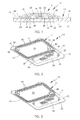
- a first embodiment of an antenna circuit 10 comprises a, preferably flexible and imageable, circuit substrate 12, an antenna coil 14, and a low-profile crossover element 16.
- the flexible imageable circuit substrate 12 is unlaminated on a rear major surface 18, thereby being devoid of an electrically conductive layer, trace or circuit in particular relating to the antenna coil 14. More particularly, the rear major surface 18 of the substrate 12 presents a plastics non-metallised surface, and conveniently is supplied as such without requiring processing to remove a conductive laminate layer therefrom.
- the substrate 12 in this embodiment, is stamped or otherwise formed to provide a continuous unbroken body portion 20 defining a display unit aperture 22, a tail portion 24 which extends in a cantilevered manner from one side of the body portion 20 and away from the display unit aperture 22, and an elongate strip-like mounting portion 26 which extends from opposing corners on a longitudinal side of the body portion 20 to encompass and thereby protect the tail portion 24.
- the substrate may be unapertured or have apertures of different sizes as necessity dictates. Additionally or alternatively, although the tail portion 24 preferably extends away from the aperture 22, it may extend into the or an aperture of the substrate, or may be dispensed with if the antenna coil 14 is entirely provided on the body portion.
- Mounting apertures 28 are provided on the substrate 12 for connection to a housing, chassis or module of a device in which the antenna circuit 10 is to be incorporated.
- two said mounting apertures 28 are provided at diametrically opposing interior corners of the body portion 20 and two said mounting apertures 28 are provided at diametrically opposing interior corners of the mounting portion 26.
- the display unit aperture 22 of the body portion 20 is dimensioned to receive a display unit 21 of a mobile point-of-sales or POS terminal 23. See Figure 9 .
- the body portion 20 therefore extends around a perimeter of a screen 25 of the display unit 21 of the POS terminal 23, sitting recessed relative thereto and just below a front surface 27 of a terminal housing 29.
- antenna circuit 10 within the terminal housing 29 and forming a wireless radio-frequency communication circuit, such as a RFID circuit or a NFC circuit, can be considered and, for example, locating the antenna circuit 10 to encircle a data-entry user-interface 31, such as a keyboard 33, provided on the front surface 27 of the terminal housing 29 may be convenient, thereby enabling a larger antenna coil to be utilised.
- a data-entry user-interface 31 such as a keyboard 33
- the body portion 20 of the substrate 12 includes an inner end portion 30 of the antenna coil 14 and an outer end portion 32. Both the inner and outer end portions 30, 32 are adjacent to a proximal end 34 of the tail portion 24.
- the antenna coil 14 extends around the body portion 20, terminating at the inner and outer end portions 30, 32, and at a free distal end 36 of the tail portion 24 in preparation for attachment of a suitable IC chip 37 (see Figure 8 ).
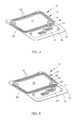
- the front major surface 38 of the substrate 12 is pre-laminated with at least one electrically conductive coating 40, for example, being or including in this case copper.
- the antenna coil 14 is formed by etching or other suitable processing, whereby the laminated electrically conductive coating 40 is partially removed down to the plastics base surface 42 of the substrate 12 to leave the electrically conductive trace 44 around the body portion 20 and along the tail portion 24.
- the laminated electrically conductive coating 40 is wholly removed from the mounting portion 26.
- the crossover element 16 therefore needs to be applied to bridge a portion 46 of the antenna coil 14 which passes between the inner and outer end portions 30, 32 and to the tail portion 24.
- the crossover element 16 of this embodiment bridges only one coil, turn or trace of the antenna coil 14, the crossover element 16 may bridge multiple coils, turns or traces passing between the inner and outer end portions 30, 32, as necessity dictates.
- an electrically insulative layer or dielectric layer 48 is first applied above and, in this case, on and overlapping the portion 46 of the trace extending between the inner and outer end portions 30, 32 of the antenna coil 14.
- the electrically insulative layer 48 has a first dimension which at least matches an outer lateral extent of the antenna coil 14, and a second dimension which at least substantially matches a separation between the inner and outer end portions 30, 32.
- the electrically insulative layer 48 may be a dielectric screen-printable UV-curable solvent-free ink, and for example may contain a urethane acrylate binder and/or magnesium silicate filler.
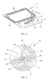
- an elongate first electrically conductive layer or trace 50 is applied above, and in this case on top of, the electrically insulative layer 48.
- a longitudinal extent of the first electrically conductive layer 50 overlaps the electrically insulative layer 48, thereby directly engaging the inner and outer end portions 30, 32 of the antenna coil 14.
- the first electrically conductive layer 50 is preferably a printable thin film ink comprising noble metal particles, such as silver.
- a noble metal is beneficial in preventing or reducing oxidation during manufacture, whilst also providing a suitable base layer for a subsequent electroplating process.
- the noble metal could be replaced or supplemented by non-noble metal electrically conductive particles, such as carbon.
- the first electrically conductive layer 50 is preferably a flowable and curable electrically conductive PTF ink, other dielectric materials and/or application processes may be considered.
- an elongate second electrically conductive layer or trace 52 is then applied above, and again in this case on top of, the first electrically conductive layer 50.
- the second electrically conductive layer 52 preferably does not contact the electrically insulative layer 48 but does engage with the first electrically conductive layer 50.
- a longitudinal extent of the second electrically conductive layer 52 is also greater than that of the first electrically conductive layer 50.
- the second electrically conductive layer 52 overlaps the first electrically conductive layer 50 in at least a longitudinal direction and directly engages the inner and outer end portions 30, 32 of the antenna coil 14 at first engagement regions 54 adjacent to second engagement regions 55 of the first electrically conductive layer 50.
- the second electrically conductive layer 52 is preferably an electroplated metal layer, in this case being copper.
- the first electrically conductive layer 50 provides a suitably platable base layer, thereby allowing the second electrically conductive layer 52 to be electroplated both thereon and onto the inner and outer end portions 30, 32 of the antenna coil 14 to complete the crossover element 16.
- the crossover element 16 can thus be more easily tuned to achieve a resistance which matches or substantially matches that of the antenna coil 14. This leads to improved antenna performance due to the lack of significant change to current flow direction and the maintenance of a common electrically conductive material, which is particularly beneficial for broadcast antennas but also useful for reading and receiving antennas.
- the retaining of a low antenna profile due to the absence of any over coating or layers on the rear major surface 18 of the substrate 12 is also beneficial in allowing incorporation of the wireless radio-frequency communication circuit to which the antenna circuit 10 forms a part into existing POS terminal designs.
- this new antenna circuit 10 can be applied to a broadcastable or non-broadcastable smart-card 70 and/or non-contact bank card 72. See Figures 8 and 9 .
- the smart-card 70 or non-contact bank card 72 comprises a card body 74 formed of top and bottom substrates 76, 78 and the circuit substrate 12 interposed there between.
- the tail portion 24 of the substrate 12 is dispensed with.
- a contact pad 80 is provided within the circuit antenna 14, and this includes an outwardly-facing electrical card-reader contact 82.
- the IC chip 37 is attached to an underside of the contact pad 80, so as to be in electrical communication therewith, using flip-chip mounting technology or any other suitable electrical connection means.
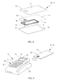
- the single-sided antenna circuit 10 comprises the circuit substrate 12, antenna coil 14 on the front major surface 38 of the substrate 12, and a crossover element 116 also on the front major surface 38 of the substrate 12.
- the crossover element 116 includes a rigid electrically insulative housing 156 for bridging the or each turn of the antenna coil 14 which passes between the inner and outer end portions 30, 32, and an electrical conductor 158 which passes through the electrically insulative housing 156 to electrically interconnect the inner and outer end portions 30, 32 of the antenna coil 14.
- the electrical conductor 158 may be formed on an electrically insulative core or former, and this may be a ceramic core or former.
- the electrical conductor 158 is formed of a same material as that of the coils, traces or turns of the antenna coil 14. Therefore, in this case, it is preferable that the electrical conductor 158 is copper.
- Terminal ends 160 of the electrical conductor 158 extend from the electrically insulative housing 156, and directly engage the inner and outer end portions 30, 32, respectively, for example, by soldering or brazing.
- a resistor 162 may have a zero ohm resistance.
- the resistor 162 may be of a higher profile than the crossover element 116 of the first embodiment, thereby making incorporation into an existing design of a device more complicated without a redesign.
- the crossover element 116 of the second embodiment may be a functional IC chip, a chip capacitor or other suitable electrical device.
- the electrically insulative housing 156 would be an IC chip housing or a capacitor housing, as required.
- such electrical device would be a dummy or passive component, being utilised solely for the purpose of the crossover and therefore not having any other function or forming a dynamic part of a circuit.
- the electrical conductor 158 of the second embodiment is of a different material than the antenna coil 14, then a circuit resistance will alter resulting in the potential of a performance drop.
- the arrangement of the second embodiment may be more suited to a non-broadcast wireless radio-communication circuit, such as that incorporated with a smart card or non-contact bank card.
- any suitable far-field or near-field wireless radio-frequency communication can utilise the above-described antenna circuit.
Landscapes
- Engineering & Computer Science (AREA)
- Health & Medical Sciences (AREA)
- Toxicology (AREA)
- Physics & Mathematics (AREA)
- Computer Networks & Wireless Communication (AREA)
- Computer Vision & Pattern Recognition (AREA)
- General Health & Medical Sciences (AREA)
- Artificial Intelligence (AREA)
- Electromagnetism (AREA)
- General Physics & Mathematics (AREA)
- Theoretical Computer Science (AREA)
- Signal Processing (AREA)
- Details Of Aerials (AREA)
- Printing Elements For Providing Electric Connections Between Printed Circuits (AREA)
- Manufacturing Of Printed Wiring (AREA)
- Near-Field Transmission Systems (AREA)
Applications Claiming Priority (1)
| Application Number | Priority Date | Filing Date | Title |
|---|---|---|---|
| CN201310357214.XA CN104377439B (zh) | 2013-08-15 | 2013-08-15 | 天线电路及制造方法 |
Publications (1)
| Publication Number | Publication Date |
|---|---|
| EP2838046A1 true EP2838046A1 (en) | 2015-02-18 |
Family
ID=51292871
Family Applications (1)
| Application Number | Title | Priority Date | Filing Date |
|---|---|---|---|
| EP14180359.3A Withdrawn EP2838046A1 (en) | 2013-08-15 | 2014-08-08 | Antenna circuit |
Country Status (6)
| Country | Link |
|---|---|
| US (1) | US9152833B2 (enExample) |
| EP (1) | EP2838046A1 (enExample) |
| JP (1) | JP6450110B2 (enExample) |
| KR (1) | KR102156821B1 (enExample) |
| CN (1) | CN104377439B (enExample) |
| BR (1) | BR102014020210A2 (enExample) |
Families Citing this family (8)
| Publication number | Priority date | Publication date | Assignee | Title |
|---|---|---|---|---|
| KR102280037B1 (ko) * | 2015-07-29 | 2021-07-21 | 삼성전자주식회사 | 디스플레이에 구비된 내장 안테나용 급전장치 |
| US10937019B2 (en) | 2016-06-08 | 2021-03-02 | Square, Inc. | Wireless communication system with auxiliary antenna |
| US10318953B2 (en) * | 2016-06-29 | 2019-06-11 | Square, Inc. | Near field communication flex circuit |
| US10594599B2 (en) | 2016-08-26 | 2020-03-17 | Cisco Technology, Inc. | Fibre channel fabric slow drain mitigation |
| US10949189B2 (en) | 2017-06-28 | 2021-03-16 | Square, Inc. | Securely updating software on connected electronic devices |
| US10635820B1 (en) | 2017-09-29 | 2020-04-28 | Square, Inc. | Update policy-based anti-rollback techniques |
| US20200409416A1 (en) * | 2019-06-27 | 2020-12-31 | Ncr Corporation | Flexible point of sale device |
| US11437851B2 (en) * | 2020-02-11 | 2022-09-06 | Dupont Electronics, Inc. | Plated copper conductor structures for wireless charging system and manufacture thereof |
Citations (10)
| Publication number | Priority date | Publication date | Assignee | Title |
|---|---|---|---|---|
| US5298687A (en) * | 1990-12-27 | 1994-03-29 | Remtec, Inc. | High-density multilayer interconnection system on a ceramic substrate for high current applications and method of manufacture |
| US20040189625A1 (en) * | 2003-03-14 | 2004-09-30 | Seiko Epson Corporation | Display device and electronic apparatus |
| EP1600887A2 (en) * | 2004-05-25 | 2005-11-30 | Nec Corporation | Mobile communication terminal |
| JP2006165050A (ja) * | 2004-12-02 | 2006-06-22 | Murata Mfg Co Ltd | トランス一体型回路基板 |
| WO2006073525A1 (en) * | 2005-01-07 | 2006-07-13 | Honeywell International Inc. | Hand held rfid reader with dipole antenna |
| WO2007019762A1 (en) * | 2005-08-19 | 2007-02-22 | Byd Company Limited | Housing for mobile phone and mobile phone having the same |
| US20070090955A1 (en) * | 2005-10-25 | 2007-04-26 | Checkpoint Systems, Inc. | Capacitor strap |
| CN101609924A (zh) * | 2008-06-20 | 2009-12-23 | 上海中京电子标签集成技术有限公司 | 一种可以实现多款芯片使用的高频标签天线 |
| EP2482261A2 (en) * | 2011-01-31 | 2012-08-01 | Metrologic Instruments, Inc. | Bar code symbol reading system employing EAS-enabling faceplate bezel |
| WO2013141658A1 (ko) * | 2012-03-23 | 2013-09-26 | 엘지이노텍 주식회사 | 안테나 어셈블리 및 그의 제조 방법 |
Family Cites Families (21)
| Publication number | Priority date | Publication date | Assignee | Title |
|---|---|---|---|---|
| JPS5989576U (ja) * | 1982-12-06 | 1984-06-18 | 株式会社東芝 | 配線用チツプ |
| JPH0465024A (ja) * | 1990-07-03 | 1992-03-02 | Rohm Co Ltd | ジャンパーチップ |
| JP2770693B2 (ja) * | 1992-12-21 | 1998-07-02 | 日本ケミコン株式会社 | 厚膜多層回路基板 |
| US5541399A (en) | 1994-09-30 | 1996-07-30 | Palomar Technologies Corporation | RF transponder with resonant crossover antenna coil |
| ATE383621T1 (de) | 1999-08-31 | 2008-01-15 | Nxp Bv | Datenträger mit integriertem schaltkreis und übertragungsspule |
| JP2001217639A (ja) * | 2000-01-31 | 2001-08-10 | Toppan Forms Co Ltd | 非接触型データ送受信体用アンテナ |
| US20020020491A1 (en) * | 2000-04-04 | 2002-02-21 | Price David M. | High speed flip chip assembly process |
| JP2002197435A (ja) * | 2000-12-27 | 2002-07-12 | Toppan Forms Co Ltd | 電子線を用いた非接触型icメディアのアンテナ回路の形成方法およびアンテナ回路を備えた非接触型icメディア |
| US6717502B2 (en) * | 2001-11-05 | 2004-04-06 | Atheros Communications, Inc. | Integrated balun and transformer structures |
| US6665193B1 (en) | 2002-07-09 | 2003-12-16 | Amerasia International Technology, Inc. | Electronic circuit construction, as for a wireless RF tag |
| US7274297B2 (en) * | 2004-07-01 | 2007-09-25 | Intermec Ip Corp. | RFID tag and method of manufacture |
| US7286053B1 (en) * | 2004-07-31 | 2007-10-23 | Kovio, Inc. | Electronic article surveillance (EAS) tag/device with coplanar and/or multiple coil circuits, an EAS tag/device with two or more memory bits, and methods for tuning the resonant frequency of an RLC EAS tag/device |
| CN2833904Y (zh) | 2005-07-29 | 2006-11-01 | 北京握奇数据系统有限公司 | 供插入式双界面智能卡使用的天线 |
| US7555826B2 (en) | 2005-12-22 | 2009-07-07 | Avery Dennison Corporation | Method of manufacturing RFID devices |
| MX2009007721A (es) * | 2007-01-18 | 2009-07-30 | Checkpoint Systems Inc | Circuito resonante permanentemente destructible con un capacitor que no es auto-regenerativo. |
| DE102007028357A1 (de) * | 2007-06-15 | 2008-12-24 | Ksw Microtec Ag | Transponderkarte |
| KR20100118103A (ko) | 2008-02-20 | 2010-11-04 | 린텍 가부시키가이샤 | 안테나회로 |
| EP2386401A1 (en) * | 2010-05-11 | 2011-11-16 | Samsung Electro-Mechanics Co., Ltd. | Case of electronic device having antenna pattern embedde therein, and mold therefor and mthod of manufacturing thereof |
| KR101179306B1 (ko) * | 2010-05-11 | 2012-09-03 | 삼성전기주식회사 | 안테나 패턴이 매립되는 전자장치의 케이스, 이의 제조금형 및 제조방법 |
| US9792985B2 (en) * | 2011-07-22 | 2017-10-17 | Virginia Tech Intellectual Properties, Inc. | Resistive volatile/non-volatile floating electrode logic/memory cell |
| CN102891359A (zh) * | 2011-07-22 | 2013-01-23 | 深圳市长盈精密技术股份有限公司 | 一种手机内置印刷天线的制作工艺 |
-
2013
- 2013-08-15 CN CN201310357214.XA patent/CN104377439B/zh not_active Expired - Fee Related
-
2014
- 2014-08-08 EP EP14180359.3A patent/EP2838046A1/en not_active Withdrawn
- 2014-08-14 BR BR102014020210A patent/BR102014020210A2/pt not_active Application Discontinuation
- 2014-08-14 KR KR1020140105912A patent/KR102156821B1/ko not_active Expired - Fee Related
- 2014-08-15 JP JP2014165358A patent/JP6450110B2/ja not_active Expired - Fee Related
- 2014-08-15 US US14/460,753 patent/US9152833B2/en not_active Expired - Fee Related
Patent Citations (11)
| Publication number | Priority date | Publication date | Assignee | Title |
|---|---|---|---|---|
| US5298687A (en) * | 1990-12-27 | 1994-03-29 | Remtec, Inc. | High-density multilayer interconnection system on a ceramic substrate for high current applications and method of manufacture |
| US20040189625A1 (en) * | 2003-03-14 | 2004-09-30 | Seiko Epson Corporation | Display device and electronic apparatus |
| EP1600887A2 (en) * | 2004-05-25 | 2005-11-30 | Nec Corporation | Mobile communication terminal |
| JP2006165050A (ja) * | 2004-12-02 | 2006-06-22 | Murata Mfg Co Ltd | トランス一体型回路基板 |
| WO2006073525A1 (en) * | 2005-01-07 | 2006-07-13 | Honeywell International Inc. | Hand held rfid reader with dipole antenna |
| WO2007019762A1 (en) * | 2005-08-19 | 2007-02-22 | Byd Company Limited | Housing for mobile phone and mobile phone having the same |
| US20070090955A1 (en) * | 2005-10-25 | 2007-04-26 | Checkpoint Systems, Inc. | Capacitor strap |
| CN101609924A (zh) * | 2008-06-20 | 2009-12-23 | 上海中京电子标签集成技术有限公司 | 一种可以实现多款芯片使用的高频标签天线 |
| EP2482261A2 (en) * | 2011-01-31 | 2012-08-01 | Metrologic Instruments, Inc. | Bar code symbol reading system employing EAS-enabling faceplate bezel |
| WO2013141658A1 (ko) * | 2012-03-23 | 2013-09-26 | 엘지이노텍 주식회사 | 안테나 어셈블리 및 그의 제조 방법 |
| EP2830152A1 (en) * | 2012-03-23 | 2015-01-28 | LG Innotek Co., Ltd. | Antenna assembly and method for manufacturing same |
Non-Patent Citations (1)
| Title |
|---|
| LOCHUN D ET AL: "Reel-to-reel manufacturability of flexible electrical interconnects and radio-frequency identification structures", 2002 PROCEEDINGS 52ND. ELECTRONIC COMPONENTS AND TECHNOLOGY CONFERENCE. ECTC 2002. SAN DIEGO, CA, MAY 28 - 31, 2002; [PROCEEDINGS OF THE ELECTRONIC COMPONENTS AND TECHNOLOGY CONFERENCE], NEW YORK, NY : IEEE, US, vol. CONF. 52, 28 May 2002 (2002-05-28), pages 686 - 689, XP010747704, ISBN: 978-0-7803-7430-0, DOI: 10.1109/ECTC.2002.1008172 * |
Also Published As
| Publication number | Publication date |
|---|---|
| KR102156821B1 (ko) | 2020-09-17 |
| KR20150020138A (ko) | 2015-02-25 |
| JP6450110B2 (ja) | 2019-01-09 |
| CN104377439B (zh) | 2019-08-27 |
| US20150048163A1 (en) | 2015-02-19 |
| CN104377439A (zh) | 2015-02-25 |
| BR102014020210A2 (pt) | 2015-12-01 |
| JP2015037327A (ja) | 2015-02-23 |
| US9152833B2 (en) | 2015-10-06 |
Similar Documents
| Publication | Publication Date | Title |
|---|---|---|
| US9152833B2 (en) | Antenna circuit | |
| US8284117B2 (en) | Antenna device and method of manufacturing the same | |
| US6665193B1 (en) | Electronic circuit construction, as for a wireless RF tag | |
| CN102576940B (zh) | 无线通信器件及金属制物品 | |
| US10387764B2 (en) | RFID tag, article including the same, and RFID tag manufacturing method | |
| US9390365B2 (en) | Integrated circuit module for a dual-interface smart card | |
| JP2009111986A (ja) | 無線周波数識別タグ装置 | |
| US9991599B2 (en) | Antenna device, electronic apparatus, and method of mounting antenna device | |
| CN107491804B (zh) | 芯片卡模块和用于制造芯片卡模块的方法 | |
| US10820418B2 (en) | Electronic module, method for manufacturing same and electronic device comprising a module of said type | |
| US10013651B2 (en) | Electronic module with three-dimensional communication interface | |
| US11948038B2 (en) | RFIC module and RFID tag | |
| KR101469764B1 (ko) | 안테나 및 그 제조방법 | |
| US9033252B2 (en) | Communication module, connector, and connector-equipped communication module | |
| JP2023537259A (ja) | スマートカードチップモジュール用の電気回路、スマートカードチップモジュール、およびスマートカードチップモジュールの製造方法 | |
| JPWO2019098123A1 (ja) | Icタグ | |
| JP2012094948A (ja) | 非接触通信記録媒体用インレット及びその製造方法及び非接触通信記録媒体 | |
| WO2021079165A1 (en) | Rfid device having an antenna with increased weight | |
| CN218996050U (zh) | 一种多功能rfid标签 | |
| JP2014220601A (ja) | アンテナ装置 | |
| US20050174745A1 (en) | Electronic assembly | |
| WO2008115022A1 (en) | Antenna for radio frequency identification and method of manufacturing the same | |
| US20120193804A1 (en) | Ohmic connection using widened connection zones in a portable electronic object | |
| US20150158307A1 (en) | Hybrid Communication Module | |
| KR101208085B1 (ko) | 디스플레이 기능이 구비된 디스플레이 온 카드 및 그 제조방법 |
Legal Events
| Date | Code | Title | Description |
|---|---|---|---|
| 17P | Request for examination filed |
Effective date: 20140808 |
|
| AK | Designated contracting states |
Kind code of ref document: A1 Designated state(s): AL AT BE BG CH CY CZ DE DK EE ES FI FR GB GR HR HU IE IS IT LI LT LU LV MC MK MT NL NO PL PT RO RS SE SI SK SM TR |
|
| AX | Request for extension of the european patent |
Extension state: BA ME |
|
| PUAI | Public reference made under article 153(3) epc to a published international application that has entered the european phase |
Free format text: ORIGINAL CODE: 0009012 |
|
| RAP1 | Party data changed (applicant data changed or rights of an application transferred) |
Owner name: JOHNSON ELECTRIC S.A. |
|
| R17P | Request for examination filed (corrected) |
Effective date: 20150813 |
|
| RBV | Designated contracting states (corrected) |
Designated state(s): AL AT BE BG CH CY CZ DE DK EE ES FI FR GB GR HR HU IE IS IT LI LT LU LV MC MK MT NL NO PL PT RO RS SE SI SK SM TR |
|
| STAA | Information on the status of an ep patent application or granted ep patent |
Free format text: STATUS: EXAMINATION IS IN PROGRESS |
|
| 17Q | First examination report despatched |
Effective date: 20180409 |
|
| RAP1 | Party data changed (applicant data changed or rights of an application transferred) |
Owner name: JOHNSON ELECTRIC INTERNATIONAL AG |
|
| RIC1 | Information provided on ipc code assigned before grant |
Ipc: G06K 7/10 20060101ALI20201015BHEP Ipc: H01Q 7/00 20060101ALI20201015BHEP Ipc: G06K 19/077 20060101ALN20201015BHEP Ipc: H01Q 1/22 20060101AFI20201015BHEP |
|
| GRAP | Despatch of communication of intention to grant a patent |
Free format text: ORIGINAL CODE: EPIDOSNIGR1 |
|
| STAA | Information on the status of an ep patent application or granted ep patent |
Free format text: STATUS: GRANT OF PATENT IS INTENDED |
|
| RIC1 | Information provided on ipc code assigned before grant |
Ipc: H01Q 7/00 20060101ALI20201019BHEP Ipc: G06K 19/077 20060101ALN20201019BHEP Ipc: G06K 7/10 20060101ALI20201019BHEP Ipc: H01Q 1/22 20060101AFI20201019BHEP |
|
| RIC1 | Information provided on ipc code assigned before grant |
Ipc: H01Q 1/22 20060101AFI20201110BHEP Ipc: G06K 7/10 20060101ALI20201110BHEP Ipc: G06K 19/077 20060101ALN20201110BHEP Ipc: H01Q 7/00 20060101ALI20201110BHEP |
|
| INTG | Intention to grant announced |
Effective date: 20201124 |
|
| STAA | Information on the status of an ep patent application or granted ep patent |
Free format text: STATUS: THE APPLICATION IS DEEMED TO BE WITHDRAWN |
|
| 18D | Application deemed to be withdrawn |
Effective date: 20210407 |