EP2834993B1 - Headset switches with crosstalk reduction - Google Patents
Headset switches with crosstalk reduction Download PDFInfo
- Publication number
- EP2834993B1 EP2834993B1 EP13716936.3A EP13716936A EP2834993B1 EP 2834993 B1 EP2834993 B1 EP 2834993B1 EP 13716936 A EP13716936 A EP 13716936A EP 2834993 B1 EP2834993 B1 EP 2834993B1
- Authority
- EP
- European Patent Office
- Prior art keywords
- jack
- ground
- switch
- terminal
- coupling
- Prior art date
- Legal status (The legal status is an assumption and is not a legal conclusion. Google has not performed a legal analysis and makes no representation as to the accuracy of the status listed.)
- Active
Links
Images


Classifications
-
- H—ELECTRICITY
- H04—ELECTRIC COMMUNICATION TECHNIQUE
- H04R—LOUDSPEAKERS, MICROPHONES, GRAMOPHONE PICK-UPS OR LIKE ACOUSTIC ELECTROMECHANICAL TRANSDUCERS; DEAF-AID SETS; PUBLIC ADDRESS SYSTEMS
- H04R1/00—Details of transducers, loudspeakers or microphones
- H04R1/10—Earpieces; Attachments therefor ; Earphones; Monophonic headphones
- H04R1/1041—Mechanical or electronic switches, or control elements
-
- H—ELECTRICITY
- H04—ELECTRIC COMMUNICATION TECHNIQUE
- H04R—LOUDSPEAKERS, MICROPHONES, GRAMOPHONE PICK-UPS OR LIKE ACOUSTIC ELECTROMECHANICAL TRANSDUCERS; DEAF-AID SETS; PUBLIC ADDRESS SYSTEMS
- H04R5/00—Stereophonic arrangements
- H04R5/04—Circuit arrangements, e.g. for selective connection of amplifier inputs/outputs to loudspeakers, for loudspeaker detection, or for adaptation of settings to personal preferences or hearing impairments
-
- H—ELECTRICITY
- H04—ELECTRIC COMMUNICATION TECHNIQUE
- H04R—LOUDSPEAKERS, MICROPHONES, GRAMOPHONE PICK-UPS OR LIKE ACOUSTIC ELECTROMECHANICAL TRANSDUCERS; DEAF-AID SETS; PUBLIC ADDRESS SYSTEMS
- H04R2420/00—Details of connection covered by H04R, not provided for in its groups
- H04R2420/05—Detection of connection of loudspeakers or headphones to amplifiers
-
- H—ELECTRICITY
- H04—ELECTRIC COMMUNICATION TECHNIQUE
- H04R—LOUDSPEAKERS, MICROPHONES, GRAMOPHONE PICK-UPS OR LIKE ACOUSTIC ELECTROMECHANICAL TRANSDUCERS; DEAF-AID SETS; PUBLIC ADDRESS SYSTEMS
- H04R2420/00—Details of connection covered by H04R, not provided for in its groups
- H04R2420/09—Applications of special connectors, e.g. USB, XLR, in loudspeakers, microphones or headphones
Definitions
- the disclosure relates to media devices, and, in particular, to techniques for reducing crosstalk caused by microphone and ground switches in an audio headset.
- Audio and other media devices often include a jack for receiving a media plug coupled to a peripheral device.
- a mobile phone may include a jack for receiving a plug coupled to an audio headset with microphone, which allows a user to carry on a voice conversation over the mobile phone using the headset.
- Other example media devices include MP3 players, handheld gaming devices, tablets, personal computers, notebook computers, personal digital assistants, etc., while other peripheral devices include headphones, hearing-aid devices, personal computer speakers, home entertainment stereo speakers, etc.
- a media device may be configured to accommodate different types of plugs, for example, a European type or a North American type.
- a plurality of switches in the media device may be selectively enabled or disabled to couple terminals of the plug to the appropriate processing nodes in the media device.
- certain of the switches designed to couple a plug terminal to a ground voltage may introduce significant on-resistance between the plug terminal and ground, which may undesirably lead to crosstalk between the left and right audio channels of the headphone.
- the switches may be made larger in size.
- such a solution would undesirably consume chip and/or board area.
- WO2011079720 (A1 ) describing a wired earphone compatible method and device.
- the method comprise: judging the type of an earphone and controlling a path switch to communicate a path that corresponds to the type of the earphone plug, according to the type of the earphone plug.
- a terminal device can be compatible with two kinds of earphones with different standards.
- US6856046 (B1 ) describing a plug-pin device discrimination circuit that is connected to the contacts of a jack.
- the discrimination circuit includes a comparison circuit, a switching network, and a controller.
- the controller operates the switching network to connect the comparison circuit to the jack contacts.
- the comparison circuit compares the electrical characteristics of at least two of the circuits contained within the plug-in device, and produces an output which varies with the results of the comparison.
- the controller receives the output of the comparison circuit and may configure additional circuitry to present an appropriate interface to the plug-in device.
- FIG 1 illustrates a block diagram of a design of a wireless communication device 100 in which the techniques of the present disclosure may be implemented.
- FIG 1 shows an example transceiver design.
- the conditioning of the signals in a transmitter and a receiver may be performed by one or more stages of amplifier, filter, upconverter, downconverter, etc.
- These circuit blocks may be arranged differently from the configuration shown in FIG 1 .
- other circuit blocks not shown in FIG 1 may also be used to condition the signals in the transmitter and receiver. Some circuit blocks in FIG 1 may also be omitted.
- wireless device 100 includes a transceiver 120 and a data processor 110.
- the data processor 110 may include a memory (not shown) to store data and program codes.
- Transceiver 120 includes a transmitter 130 and a receiver 150 that support bi-directional communication.
- wireless device 100 may include any number of transmitters and any number of receivers for any number of communication systems and frequency bands. All or a portion of transceiver 120 may be implemented on one or more analog integrated circuits (ICs), RF ICs (RFICs), mixed-signal ICs, etc.
- ICs analog integrated circuits
- RFICs RF ICs
- mixed-signal ICs etc.
- a transmitter or a receiver may be implemented with a super-heterodyne architecture or a direct-conversion architecture.
- a signal is frequency converted between radio frequency (RF) and baseband in multiple stages, e.g., from RF to an intermediate frequency (IF) in one stage, and then from IF to baseband in another stage for a receiver.
- IF intermediate frequency
- the direct-conversion architecture a signal is frequency converted between RF and baseband in one stage.
- the super-heterodyne and direct-conversion architectures may use different circuit blocks and/or have different requirements.
- transmitter 130 and receiver 150 are implemented with the direct-conversion architecture.
- data processor 110 processes data to be transmitted and provides I and Q analog output signals to transmitter 130.
- the data processor 110 includes digital-to-analog-converters (DAC's) 114a and 114b for converting digital signals generated by the data processor 110 into the I and Q analog output signals, e.g., I and Q output currents, for further processing.
- DAC's digital-to-analog-converters
- lowpass filters 132a and 132b filter the I and Q analog output signals, respectively, to remove undesired images caused by the prior digital-to-analog conversion.
- Amplifiers (Amp) 134a and 134b amplify the signals from lowpass filters 132a and 132b, respectively, and provide I and Q baseband signals.
- An upconverter 140 upconverts the I and Q baseband signals with I and Q transmit (TX) local oscillating (LO) signals from a TX LO signal generator 190 and provides an upconverted signal.
- a filter 142 filters the upconverted signal to remove undesired images caused by the frequency upconversion as well as noise in a receive frequency band.
- a power amplifier (PA) 144 amplifies the signal from filter 142 to obtain the desired output power level and provides a transmit RF signal.
- the transmit RF signal is routed through a duplexer or switch 146 and transmitted via an antenna 148.
- antenna 148 receives signals transmitted by base stations and provides a received RF signal, which is routed through duplexer or switch 146 and provided to a low noise amplifier (LNA) 152.
- the received RF signal is amplified by LNA 152 and filtered by a filter 154 to obtain a desirable RF input signal.
- a downconverter 160 downconverts the RF input signal with I and Q receive (RX) LO signals from an RX LO signal generator 180 and provides I and Q baseband signals.
- the I and Q baseband signals are amplified by amplifiers 162a and 162b and further filtered by lowpass filters 164a and 164b to obtain I and Q analog input signals, which are provided to data processor 110.
- the data processor 110 includes analog-to-digital-converters (ADC's) 116a and 116b for converting the analog input signals into digital signals to be further processed by the data processor 110.
- ADC's analog-to-digital-converters
- TX LO signal generator 190 generates the I and Q TX LO signals used for frequency upconversion.
- RX LO signal generator 180 generates the I and Q RX LO signals used for frequency downconversion.
- Each LO signal is a periodic signal with a particular fundamental frequency.
- a PLL 192 receives timing information from data processor 110 and generates a control signal used to adjust the frequency and/or phase of the TX LO signals from LO signal generator 190.
- a PLL 182 receives timing information from data processor 110 and generates a control signal used to adjust the frequency and/or phase of the RX LO signals from LO signal generator 180.
- the data processor 110 further includes a baseband processing module 101 configured to process RX data from the ADC's 116a, 116b, and further to process TX data to the DAC's 114a, 114b.
- the baseband processing module 101 is further coupled to an audio codec 102.
- the module 101 may transmit digital signals to the audio codec 102 for output as an analog audio signal, and may further receive digital signals from the audio codec 102 corresponding to audio input signals.
- the audio codec 102 may further interface with audio signals to and from a headset (not shown in FIG 1 ).
- the techniques of the present disclosure may be implemented, e.g., using switches integrated on the data processor 110 with the audio codec 102, or using switches that are external to the data processor 110.
- FIG 2 illustrates an exemplary scenario 200 wherein the techniques of the present disclosure may be applied.
- FIG 2 is shown for illustrative purposes only, and is not meant to limit the scope of the present disclosure to the particular system shown.
- the techniques disclosed herein may also be readily applied to audio devices other than that shown in FIG 2 .
- the techniques may also be readily adapted to other types of multimedia devices, as well as to non-audio media devices, e.g., to reduce crosstalk in plugs supporting video, etc.
- Such alternative exemplary embodiments are contemplated to be within the scope of the present disclosure.
- a headset 210 includes a left (L) headphone 215, a right (R) headphone 220, and a microphone 230. These components of the headset 210 are electrically coupled to terminals of a plug 250 via conducting wires 245.
- the plug 250 is insertable into a jack 260 of a media device 240. Note the jack 260 need not extrude from the surface of the device 240 as suggested by FIG 2 , and furthermore, the sizes of the elements shown in FIG 2 are not necessarily drawn to scale.
- the device 240 may be a mobile phone incorporating the circuitry shown in FIG 1 .
- the device 240 may also be, e.g., an MP3 player, home stereo system, etc.
- Audio and/or other signals may be exchanged between the device 240 and the headset 210 through the plug 250 and jack 260.
- the plug 250 receives the audio signals from the jack 260, and routes the signals to the L and R headphones of the headset 210.
- the plug 250 may further couple an electrical signal with audio content generated by the microphone 230 to the jack 260, and the microphone signal may be further processed by the device 240.
- the plug 250 may include further terminals not shown, e.g., for communicating other types of signals such as control signals, video signals, etc.
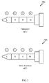
- the sequence of terminals on plug 250 may generally be provided according to one of several types of common standardized layouts, as shown in FIG 3 .
- the terminals may be ordered as left audio (L), right audio (R), microphone (M), and ground (G), as enumerated from the tip of the plug to the base of the plug.
- the terminals may be ordered as left audio (L), right audio (R), ground (G), and microphone (M).
- the terminals of both types of plugs may be electrically coupled to corresponding jack terminals 1, 2, 3, and 4, respectively, from tip to base, as indicated by the circled numerals in FIG 3 .
- a device 240 may generally incorporate switching circuitry to electrically route the plug terminals to the appropriate jack terminals, depending on the type of plug inserted. For example, a plurality of switches may be provided at the device 240 to electrically couple terminals (M) and (G) of a European type plug to terminals 3 and 4 of a jack, respectively, or alternatively, to couple terminals (G) and (M) of a North American type plug to terminals 3 and 4 of a jack, respectively.
- the device 240 may include a codec chip (not shown) on which the drivers (e.g., amplifiers) for the left (L) and right (R) audio channels may be provided, and the switching circuitry may be integrated with the codec chip, or they may be external to the codec chip.
- the drivers e.g., amplifiers
- the switching circuitry may be integrated with the codec chip, or they may be external to the codec chip.
- a first terminal of a jack may denote, e.g., any of jack terminals 1, 2, 3, and 4 shown in FIG 3
- a second terminal of a jack may denote, e.g., any of jack terminals 1, 2, 3, and 4 distinct from the "first terminal.”
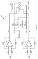
- FIG 4 illustrates a prior art implementation of an electrical system 400, e.g., provided on a device 240, for driving jack terminals 1 through 4, wherein a plurality of switches are provided to accommodate both North American and European type plugs.
- an amplifier 410R is configured with resistors R1a, R1b, R2a, R2b for generating a right headphone signal (H_R) for driving terminal 2 of the jack.
- H_R right headphone signal
- the H_R signal will correspond to an amplified version of a differential (diff) right-channel input signal IN_R.
- FIG 4 further illustrates an amplifier 410L configured with resistors R1a', R1b', R2a', R2b' for generating a left headphone signal (H_L) for driving terminal 1 of the jack.
- the H_L signal will also correspond to an amplified version of a differential (diff) left-channel input signal IN_L.
- resistors in FIG 4 is shown for illustrative purposes only, and it is contemplated that alternative exemplary embodiments may incorporate other amplifier configurations for driving the left and right audio channels, e.g., amplifiers having different types of feedback or passive elements than shown in FIG 4 .
- H_REF resistors R2b and R2a' are coupled at a single node labeled H_REF, which is in turn coupled to the ground (GND) voltage.
- H_REF may also be denoted the "reference terminal” or “ground sensing input” or “ground sensing terminal.” It will be appreciated that H_REF may be understood to provide a common-mode reference to the differential amplifiers 410R and 410L. For example, to reduce common-mode ground noise that may be present at the jack ground terminal and at the board level, H_REF may be connected directly to the jack ground terminal to remove the ground noise.
- a plurality of switches S1, S2, S3, and S4 is further provided to alternately couple the ground (GND) and microphone (MIC) nodes of the system 400 to the appropriate terminals of the jack 260, depending on the inserted plug type.
- GND ground
- MIC microphone
- One disadvantage of the system 400 is that a certain degree of crosstalk may be present between the right and left audio channels H_R and H_L, due to finite on-resistance of either of the ground switches S1 or S2.
- a resistance RG between the jack terminal and the system ground voltage
- a resistance RM between the jack terminal and the microphone node, wherein RG corresponds to the on-resistance of either switch S1 or S2, while RM corresponds to the on-resistance of either switch S3 or S4.
- the ground switch on-resistance RG will generate a crosstalk component between the right and left headphone channels.
- a component in the left audio signal H_L will be present in the right audio signal H_R, and vice versa, due to the varying voltage across the common ground switch resistance RG.
- a 16-Ohm switch resistance can create approximately -60 dB of crosstalk when coupled with a 16-milliOhm headset. Such crosstalk undesirably degrades the signal fidelity of the left and right audio channels.
- Crosstalk RG RL + 2 ⁇ RG ; wherein RL represents the resistance corresponding to the left or right audio load.
- RG ground switch resistance
- RL the resistance corresponding to the left or right audio load.
- the switches S1 and S2 may be made larger in size to reduce their turn-on resistance.
- this may undesirably consume a great deal of silicon chip area, and is not an ideal solution for integrated systems, wherein chip area is at a premium. It would thus be desirable to provide simple and efficient techniques to reduce the amount of crosstalk in an audio system.
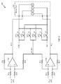
- FIG 6 illustrates an exemplary embodiment of the present disclosure, wherein a six-switch solution is provided to reduce the aforementioned crosstalk. Note certain aspects of FIG 6 are shown for illustrative purposes only, and are not meant to limit the scope of the present disclosure to the specific embodiment shown. Furthermore, certain elements may be similarly labeled in FIGs 4 and 6 , and such elements may be understood as performing similar functionality, unless otherwise noted.
- switches S5 and S6 are provided in the audio system, in addition to the switches S1-S4.
- S5 and S6 are configured to always couple the ground sensing input H_REF to the ground terminal of the jack 260, regardless of whether the plug type is North American or European. In this manner, any voltage drops caused by RG may be sampled by H_REF and fed back to the audio amplifiers as common-mode ground noise.
- S5 couples H_REF to terminal 4 of the jack 260.
- S6 couples H_REF to terminal 3 of the jack 260.
- FIG 7 illustrates electrical connections of the system 600 according to both the ⁇ 1 and ⁇ 2 configurations of the switches.
- the reference node H_REF is configured to sample the voltage across RG via a resistance RF, which may correspond to the on-resistance of the switch S5 or S6.
- RF resistance
- RF may be on the order of a few Ohms, while the resistors R1a, R2a, R1b, R2b, R1a', R2a', R1b', R2b' may all be on the order of kiloOhms. Therefore, any crosstalk contributed by RF is not expected to be significant.
- any crosstalk contributed by RF can be further reduced by using integrated circuit layout techniques to match the resistances in the amplifier (410R and 410L) feedback paths to each other.
- FIG 8 illustrates an exemplary embodiment of the present disclosure, wherein the six switches S1-S6 are provided in discrete form, i.e., separately from an integrated circuit housing the right channel amplifier 8200 and left channel amplifier 8300.
- each of the switches S1-S6 is associated with two corresponding pins, corresponding to the switch terminals.
- S1 has two pins S1.1, S1.2
- S2 has two pins S2.1, S2.2, etc.
- the pins may correspond to, e.g., physical pins of a discrete integrated circuit housing the corresponding switch or switches.
- all six of the switches S1-S6 may be provided on a single discrete integrated circuit, with twelve physical pins provided for interfacing the switches with other board-level elements.
- any subset of the switches S1-S6 may be provided on single discrete integrated circuits, with a total of twelve physical pins provided across all the discrete integrated circuits housing the switches.
- the headset jack 260 is further shown with four physical terminals 260.1, 260.2, 260.3, and 260.4, which are electrically coupled to the corresponding terminals 1, 2, 3, and 4 of the jack 260, as earlier described hereinabove.
- the pins S1.2, S2.2, S3.2, S4.2, S5.2, and S6.2, representing the outputs of the switches S1-S6, may be routed to corresponding physical terminals 260.1, 260.2, 260.3, 260.4 using board trace routing 801, i.e., conductive electrical leads that are provided on a physical board on which the switches S1-S6, the jack 260, as well as an integrated circuit housing amplifiers 8200, 8300 may be provided.
- S1.2 and S3.2 are electrically coupled, and similarly, S2.2 and S4.2 are electrically coupled.
- the output of pin S5.2 is electrically coupled to physical terminal 260.4 of the jack 260.
- the electrical connection between S5.2 and 160.4 may be provided as close to 260.4 as possible, i.e., in close physical proximity to the jack 160.
- the output of pin S6.2 is electrically coupled to physical terminal 260.3 of the jack 260, and the electrical connection between S6.2 and 260.3 may be provided as close to 260.3 as possible.
- the electrical connection between pin S5.2 and terminal 260.4 is effectively independent of the electrical connection between pins S1.2, S3.2 and terminal 260.4, since the two electrical connections are routed over separate conductive paths on the board.
- the parasitic routing resistance between S1.2, S3.2 and jack terminal 260.4 can be modeled as being part of the ground resistance RG, and the parasitic routing resistance between S5.2 and 260.4 can be modeled as being part of the ground sensing path resistance RF.
- the electrical connection between pin S6.2 and terminal 260.3 is effectively independent of the electrical connection between pins S2.2, S4.2 and terminal 260.3.
- the parasitic routing resistance between S2.2, S4.2 and jack terminal 260.3 can be modeled as being part of the ground resistance RG, and the parasitic routing resistance between S6.2 and 260.3 can be modeled as being part of the ground sensing path resistance RF.
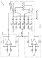
- FIG 9 illustrates an alternative exemplary embodiment of the present disclosure, wherein the six switches S1-S6 are provided on a single integrated circuit, on which the audio amplifiers are also provided.
- an integrated circuit 910 includes all of switches S1-S6, as well as amplifiers 410R, 410L, and associated resistances.
- the integrated circuit 910 may include further features, e.g., audio codec functionality and other control functionality.
- the integrated circuit 910 includes six physical (package) pins 910.1, 910.2, 910.3, 910.4, 910.5, and 910.6 for interfacing with other board-level components.
- these pins may be routed to physical terminals 260.1, 260.2, 260.3, 260.4 of the jack 260 using board trace routing 901.
- Pins 910.1 and 910.6 are used for delivery of the audio signals H_R and H_L, respectively, to physical terminals 260.2, 260.1 of the jack 260.
- Pins 910.2, 910.3, 910.4, 910.5 are coupled to terminals 260.4 and 260.3.
- the electrical connection between 910.3 and 260.4 may be provided as close to 260.4 as possible, i.e., in close physical proximity to the jack 260.
- the output of pin 910.4 is electrically coupled to physical terminal 260.3 of the jack 260, and the electrical connection between 910.4 and 260.3 may be provided as close to 260.3 as possible.
- FIG 10 illustrates an exemplary embodiment according to the present disclosure for supporting both an FM antenna and North American / European-type headset compatibility.
- GND and MIC are selectively coupled to terminals 4 and 3 of the jack via ferrite beads 702, 704 and filtering capacitors 712, 714, as shown in FIG 7 .
- H_REF is further shown selectively coupled to either terminal 4 or 3 via ferrite bead 706 or 708, and filtering capacitor 716 or 718.
- the values of the ferrite beads and filtering capacitors may be chosen to isolate GND, MIC, and H_REF from other portions of the circuitry at certain frequencies, e.g., to isolate such nodes from an FM antenna / receiver module 790 as further described hereinbelow.
- the FM module 790 includes capacitors (Csmall) 792, 794 coupling nodes 3 and 4 of the jack to an inductor (Ltune) 796, a capacitor (Cmatch) 798, and another inductor (Lmatch) 799 as shown.
- Lmatch 799 may be coupled to FM receive processing circuitry (not shown in FIG 10 ) to, e.g., process an FM radio signal as received over the air via the conducting wires 245 of the headset 210.
- the conducting wires 245 in particular, the wires of the headset making electrical contact with terminals 3 and 4 of the jack
- the FM signals will be effectively frequency multiplexed with the audio signals over the conducting wires 245.
- the six-switch crosstalk reduction techniques of the present disclosure may advantageously be combined with techniques to receive an FM signal using the wires 245 of the headset.
- the ferrite beads and capacitors may be provided as filtering elements to protect the codec chip (e.g., the circuitry for processing H_R, H_L, H_REF, and MIC) from, e.g., RF inter-modulation.
- the filtering elements may further protect the FM processing circuitry 791 from RF spurs arising from the codec chip.
- all the switches S1-S6 shown in FIG 10 may be provided externally to the codec integrated circuit.
- the two ferrite beads 702, 704 and filtering capacitors 712, 714 may be removed to reduce the external component count, at the cost of potentially degraded crosstalk performance.
- FIG 11 illustrates an alternative exemplary embodiment, wherein the plurality of switches S1-S6 is integrated on a single chip with the codec.
- elements enclosed by the edges of the dashed box 8100 may correspond to elements found on the codec integrated circuit, while other elements not enclosed by 8100 may be provided externally to the integrated circuit.
- a plurality of pins 822, 824 is provided to couple the outputs of switches S5 and S6 from the integrated circuit to the corresponding passive elements and terminals of the jack, independently of the pins 826, 828 dedicated to the other switches S1 through S4.
- the H_REF node will not share the same off-chip routing path with the codec system ground node, thereby advantageously reducing any further crosstalk associated with having these nodes share the same off-chip routing path.
- the parasitic resistance from any external inductor (or beads) can be treated as part of the RG and RF in the equivalent circuit, and thus Equation (2) also applies in this case.
- the ferrite beads 802, 804 and filtering capacitors 812, 814 may also be made optional in certain exemplary embodiments.
- FIG 12 illustrates an exemplary embodiment of a method according to the present disclosure. Note FIG 12 is described for illustrative purposes only, and is not meant to limit the scope of the present disclosure to any particular method described herein.
- a first terminal of a jack is selectively coupled to a ground connection using a first ground switch.
- a second terminal of the jack is selectively coupled to the ground connection using the second ground switch.
- the first terminal of the jack is selectively coupled to a microphone node using a first microphone switch.
- the second terminal of the jack is selectively coupled to the microphone node using a second microphone switch.
- the first terminal of the jack is selectively coupled to a ground sensing input using a first ground sensing switch.
- the second terminal of the jack is selectively coupled to the ground sensing input using a second ground sensing switch.
- the switches are selectively coupled depending on whether the jack is detected to be of a North American or a European type.
- DSP Digital Signal Processor
- ASIC Application Specific Integrated Circuit
- FPGA Field Programmable Gate Array
- a general purpose processor may be a microprocessor, but in the alternative, the processor may be any conventional processor, controller, microcontroller, or state machine.
- a processor may also be implemented as a combination of computing devices, e.g., a combination of a DSP and a microprocessor, a plurality of microprocessors, one or more microprocessors in conjunction with a DSP core, or any other such configuration.
- a software module may reside in Random Access Memory (RAM), flash memory, Read Only Memory (ROM), Electrically Programmable ROM (EPROM), Electrically Erasable Programmable ROM (EEPROM), registers, hard disk, a removable disk, a CD-ROM, or any other form of storage medium known in the art.
- An exemplary storage medium is coupled to the processor such that the processor can read information from, and write information to, the storage medium.
- the storage medium may be integral to the processor.
- the processor and the storage medium may reside in an ASIC.
- the ASIC may reside in a user terminal.
- the processor and the storage medium may reside as discrete components in a user terminal.
- the functions described may be implemented in hardware, software, firmware, or any combination thereof. If implemented in software, the functions may be stored on or transmitted over as one or more instructions or code on a computer-readable medium.
- Computer-readable media includes both computer storage media and communication media including any medium that facilitates transfer of a computer program from one place to another.
- a storage media may be any available media that can be accessed by a computer.
- such computer-readable media can comprise RAM, ROM, EEPROM, CD-ROM or other optical disk storage, magnetic disk storage or other magnetic storage devices, or any other medium that can be used to carry or store desired program code in the form of instructions or data structures and that can be accessed by a computer.
- any connection is properly termed a computer-readable medium.
- the software is transmitted from a website, server, or other remote source using a coaxial cable, fiber optic cable, twisted pair, digital subscriber line (DSL), or wireless technologies such as infrared, radio, and microwave
- the coaxial cable, fiber optic cable, twisted pair, DSL, or wireless technologies such as infrared, radio, and microwave are included in the definition of medium.
- Disk and disc includes compact disc (CD), laser disc, optical disc, digital versatile disc (DVD), floppy disk and Blu-Ray disc where disks usually reproduce data magnetically, while discs reproduce data optically with lasers. Combinations of the above should also be included within the scope of computer-readable media.
Landscapes
- Physics & Mathematics (AREA)
- Engineering & Computer Science (AREA)
- Acoustics & Sound (AREA)
- Signal Processing (AREA)
- Amplifiers (AREA)
- Circuit For Audible Band Transducer (AREA)
- Headphones And Earphones (AREA)
Applications Claiming Priority (3)
| Application Number | Priority Date | Filing Date | Title |
|---|---|---|---|
| US201261621266P | 2012-04-06 | 2012-04-06 | |
| US13/570,068 US8917882B2 (en) | 2012-04-06 | 2012-08-08 | Headset switches with crosstalk reduction |
| PCT/US2013/035522 WO2013152332A1 (en) | 2012-04-06 | 2013-04-05 | Headset switches with crosstalk reduction |
Publications (2)
| Publication Number | Publication Date |
|---|---|
| EP2834993A1 EP2834993A1 (en) | 2015-02-11 |
| EP2834993B1 true EP2834993B1 (en) | 2016-09-14 |
Family
ID=49292318
Family Applications (1)
| Application Number | Title | Priority Date | Filing Date |
|---|---|---|---|
| EP13716936.3A Active EP2834993B1 (en) | 2012-04-06 | 2013-04-05 | Headset switches with crosstalk reduction |
Country Status (6)
| Country | Link |
|---|---|
| US (1) | US8917882B2 (enExample) |
| EP (1) | EP2834993B1 (enExample) |
| JP (1) | JP2015518323A (enExample) |
| CN (1) | CN104160718B (enExample) |
| TW (1) | TW201404184A (enExample) |
| WO (1) | WO2013152332A1 (enExample) |
Families Citing this family (17)
| Publication number | Priority date | Publication date | Assignee | Title |
|---|---|---|---|---|
| CN102780950B (zh) * | 2012-07-10 | 2014-09-03 | 环汇系统有限公司 | 电子设备音频控制系统及其控制方法 |
| CN102883255B (zh) * | 2012-09-13 | 2014-12-03 | 天地融科技股份有限公司 | 转接装置、电子签名工具、检测装置和接口检测系统 |
| US9338570B2 (en) * | 2013-10-07 | 2016-05-10 | Nuvoton Technology Corporation | Method and apparatus for an integrated headset switch with reduced crosstalk noise |
| CN104618666B (zh) * | 2013-11-05 | 2018-04-10 | 南宁富桂精密工业有限公司 | 音频信号控制电路 |
| TWI572212B (zh) * | 2013-11-20 | 2017-02-21 | 瑞昱半導體股份有限公司 | 應用於耳機麥克風組的訊號處理電路及訊號處理方法 |
| GB2527844A (en) * | 2014-07-04 | 2016-01-06 | Isis Innovation | Sensor assembly |
| WO2016192091A1 (en) * | 2015-06-04 | 2016-12-08 | Cirrus Logic International Semiconductor Ltd. | Audio connector and circuitry |
| US20170111742A1 (en) * | 2015-09-11 | 2017-04-20 | Ess Technology, Inc. | Apparatus and Method for Driving Headphones Differentially in Mobile Applications |
| US9888318B2 (en) * | 2015-11-25 | 2018-02-06 | Mediatek, Inc. | Method, system and circuits for headset crosstalk reduction |
| US9977755B2 (en) * | 2016-03-24 | 2018-05-22 | Qualcomm Incorporated | Mobile device with multiple communication capabilities |
| CN106791076A (zh) * | 2016-12-16 | 2017-05-31 | 惠州Tcl移动通信有限公司 | 基于移动终端上的智键控制智能led灯的方法及系统 |
| TWI633794B (zh) * | 2017-01-13 | 2018-08-21 | 茂達電子股份有限公司 | 零噪音耳麥偵測電路 |
| CN109842836B (zh) * | 2017-11-27 | 2021-06-15 | 华为终端有限公司 | 一种消除音频信号播放通路之间串扰的方法、电路及设备 |
| CN110719548B (zh) * | 2018-07-12 | 2022-04-29 | 中兴通讯股份有限公司 | 音频处理装置、音频串扰处理方法及装置 |
| CN108966072A (zh) * | 2018-09-27 | 2018-12-07 | 中新工程技术研究院有限公司 | 一种头戴式耳机、一种切换方法及切换系统 |
| RU2727339C1 (ru) * | 2019-09-18 | 2020-07-21 | Федеральное государственное бюджетное образовательное учреждение высшего образования "Московский государственный технологический университет "СТАНКИН" (ФГБОУ ВО "МГТУ "СТАНКИН") | Способ вывода звуковой информации о технологическом процессе электронно-пучкового воздействия |
| US12047758B2 (en) | 2022-01-20 | 2024-07-23 | Qualcomm Incorporated | Audio ground switch channel crosstalk cancellation technique |
Family Cites Families (13)
| Publication number | Priority date | Publication date | Assignee | Title |
|---|---|---|---|---|
| JP2560247Y2 (ja) * | 1992-07-22 | 1998-01-21 | オンキヨー株式会社 | ヘッドホン出力回路 |
| US6856046B1 (en) | 2002-03-08 | 2005-02-15 | Analog Devices, Inc. | Plug-in device discrimination circuit and method |
| US7450726B2 (en) | 2004-03-11 | 2008-11-11 | Texas Instruments Incorporated | Headset detector in a device generating audio signals |
| JP4929960B2 (ja) * | 2006-10-06 | 2012-05-09 | ソニー株式会社 | オーディオ再生装置、計測方法、プログラム、記録媒体、音漏れ低減調整方法 |
| US7912501B2 (en) | 2007-01-05 | 2011-03-22 | Apple Inc. | Audio I/O headset plug and plug detection circuitry |
| US8362654B2 (en) * | 2007-11-21 | 2013-01-29 | Nokia Corporation | Electronic device interface switching system |
| US8150046B2 (en) * | 2009-02-26 | 2012-04-03 | Research In Motion Limited | Audio jack for a portable electronic device |
| CA2661693C (en) | 2009-04-08 | 2015-06-23 | Sennheiser Electronic Gmbh & Co. Kg | Headset and headset cable |
| US7928392B1 (en) * | 2009-10-07 | 2011-04-19 | T-Ray Science Inc. | Systems and methods for blind echo cancellation |
| CN101719610A (zh) * | 2009-12-30 | 2010-06-02 | 华为终端有限公司 | 一种有线耳机兼容方法和装置 |
| US8452024B2 (en) | 2010-04-29 | 2013-05-28 | Texas Instruments Incorporated | Ground loop noise rejection for a headset subsystem |
| CN201781618U (zh) * | 2010-08-27 | 2011-03-30 | 广东长虹数码科技有限公司 | 一种可靠性高的耳机检测电路 |
| CN102404665B (zh) * | 2010-09-07 | 2016-12-07 | 中兴通讯股份有限公司 | 一种耳机接口自适应电路 |
-
2012
- 2012-08-08 US US13/570,068 patent/US8917882B2/en active Active
-
2013
- 2013-04-05 WO PCT/US2013/035522 patent/WO2013152332A1/en not_active Ceased
- 2013-04-05 CN CN201380011987.0A patent/CN104160718B/zh active Active
- 2013-04-05 JP JP2015504760A patent/JP2015518323A/ja active Pending
- 2013-04-05 EP EP13716936.3A patent/EP2834993B1/en active Active
- 2013-04-08 TW TW102112373A patent/TW201404184A/zh unknown
Also Published As
| Publication number | Publication date |
|---|---|
| US8917882B2 (en) | 2014-12-23 |
| JP2015518323A (ja) | 2015-06-25 |
| CN104160718A (zh) | 2014-11-19 |
| US20130266146A1 (en) | 2013-10-10 |
| EP2834993A1 (en) | 2015-02-11 |
| WO2013152332A1 (en) | 2013-10-10 |
| CN104160718B (zh) | 2018-12-04 |
| TW201404184A (zh) | 2014-01-16 |
Similar Documents
| Publication | Publication Date | Title |
|---|---|---|
| EP2834993B1 (en) | Headset switches with crosstalk reduction | |
| US9338570B2 (en) | Method and apparatus for an integrated headset switch with reduced crosstalk noise | |
| US9380388B2 (en) | Channel crosstalk removal | |
| KR102105315B1 (ko) | 검출 회로 | |
| WO2014032482A1 (en) | System and method for detecting the ground and microphone input contacts in an audio plug | |
| US9077342B2 (en) | Circuit assembly for processing an electrical signal of a microphone | |
| KR101710174B1 (ko) | 통합 헤드셋의 크로스토크 감소 방법 및 장치 | |
| EP4377807B1 (en) | Universal serial bus (usb) host data switch with integrated equalizer | |
| WO2012068985A1 (zh) | 伪差分音频输入电路及其设置方法 | |
| CN113810816B (zh) | 耳机、调频信号接收系统和方法 | |
| CN112468113B (zh) | 基于源极跟随器的Sallen-Key架构 | |
| EP2552018A1 (en) | Microphone preamplifier circuit | |
| CN102138320A (zh) | 对信号路径上的接地参考进行驱动的方法、对信号路径上的接地参考进行驱动的控制电路,以及移动设备 | |
| US20050036644A1 (en) | Adapter for connecting a mobile phone stereoearphone-microphone set to a stereo system | |
| EP3063927A1 (en) | Infotainment system | |
| CN102572632A (zh) | 具有耳机接口的车载信息系统装置 | |
| EP2716066B1 (en) | Circuit assembly for processing an electrical signal of a microphone | |
| EP2879403A1 (en) | Downlink transmission device for audio signal and electronic signature tool | |
| CN111818424B (zh) | 一种音频播放电路 | |
| US20250247078A1 (en) | Hybrid lattice filter | |
| JP5811630B2 (ja) | 電力増幅器、及び、電子装置 | |
| JP2012501560A (ja) | マルチポートコネクタの出力信号における外乱の低減 | |
| JP2024043354A (ja) | スイッチ回路 | |
| KR20160144376A (ko) | 클래스-g/h 헤드폰들을 위한 fm 필터링 | |
| Liang | Low noise amplifier design and noise cancellation for wireless hearing aids |
Legal Events
| Date | Code | Title | Description |
|---|---|---|---|
| PUAI | Public reference made under article 153(3) epc to a published international application that has entered the european phase |
Free format text: ORIGINAL CODE: 0009012 |
|
| 17P | Request for examination filed |
Effective date: 20141103 |
|
| AK | Designated contracting states |
Kind code of ref document: A1 Designated state(s): AL AT BE BG CH CY CZ DE DK EE ES FI FR GB GR HR HU IE IS IT LI LT LU LV MC MK MT NL NO PL PT RO RS SE SI SK SM TR |
|
| AX | Request for extension of the european patent |
Extension state: BA ME |
|
| DAX | Request for extension of the european patent (deleted) | ||
| GRAP | Despatch of communication of intention to grant a patent |
Free format text: ORIGINAL CODE: EPIDOSNIGR1 |
|
| INTG | Intention to grant announced |
Effective date: 20160407 |
|
| RIN1 | Information on inventor provided before grant (corrected) |
Inventor name: MIAO, GUOQING Inventor name: SHAH, PETER J. |
|
| GRAS | Grant fee paid |
Free format text: ORIGINAL CODE: EPIDOSNIGR3 |
|
| GRAA | (expected) grant |
Free format text: ORIGINAL CODE: 0009210 |
|
| AK | Designated contracting states |
Kind code of ref document: B1 Designated state(s): AL AT BE BG CH CY CZ DE DK EE ES FI FR GB GR HR HU IE IS IT LI LT LU LV MC MK MT NL NO PL PT RO RS SE SI SK SM TR |
|
| REG | Reference to a national code |
Ref country code: GB Ref legal event code: FG4D |
|
| REG | Reference to a national code |
Ref country code: CH Ref legal event code: EP |
|
| REG | Reference to a national code |
Ref country code: IE Ref legal event code: FG4D |
|
| REG | Reference to a national code |
Ref country code: AT Ref legal event code: REF Ref document number: 830131 Country of ref document: AT Kind code of ref document: T Effective date: 20161015 |
|
| REG | Reference to a national code |
Ref country code: DE Ref legal event code: R096 Ref document number: 602013011512 Country of ref document: DE |
|
| REG | Reference to a national code |
Ref country code: LT Ref legal event code: MG4D |
|
| REG | Reference to a national code |
Ref country code: NL Ref legal event code: MP Effective date: 20160914 |
|
| PG25 | Lapsed in a contracting state [announced via postgrant information from national office to epo] |
Ref country code: RS Free format text: LAPSE BECAUSE OF FAILURE TO SUBMIT A TRANSLATION OF THE DESCRIPTION OR TO PAY THE FEE WITHIN THE PRESCRIBED TIME-LIMIT Effective date: 20160914 Ref country code: NO Free format text: LAPSE BECAUSE OF FAILURE TO SUBMIT A TRANSLATION OF THE DESCRIPTION OR TO PAY THE FEE WITHIN THE PRESCRIBED TIME-LIMIT Effective date: 20161214 Ref country code: LT Free format text: LAPSE BECAUSE OF FAILURE TO SUBMIT A TRANSLATION OF THE DESCRIPTION OR TO PAY THE FEE WITHIN THE PRESCRIBED TIME-LIMIT Effective date: 20160914 Ref country code: HR Free format text: LAPSE BECAUSE OF FAILURE TO SUBMIT A TRANSLATION OF THE DESCRIPTION OR TO PAY THE FEE WITHIN THE PRESCRIBED TIME-LIMIT Effective date: 20160914 Ref country code: FI Free format text: LAPSE BECAUSE OF FAILURE TO SUBMIT A TRANSLATION OF THE DESCRIPTION OR TO PAY THE FEE WITHIN THE PRESCRIBED TIME-LIMIT Effective date: 20160914 |
|
| REG | Reference to a national code |
Ref country code: AT Ref legal event code: MK05 Ref document number: 830131 Country of ref document: AT Kind code of ref document: T Effective date: 20160914 |
|
| PG25 | Lapsed in a contracting state [announced via postgrant information from national office to epo] |
Ref country code: SE Free format text: LAPSE BECAUSE OF FAILURE TO SUBMIT A TRANSLATION OF THE DESCRIPTION OR TO PAY THE FEE WITHIN THE PRESCRIBED TIME-LIMIT Effective date: 20160914 Ref country code: GR Free format text: LAPSE BECAUSE OF FAILURE TO SUBMIT A TRANSLATION OF THE DESCRIPTION OR TO PAY THE FEE WITHIN THE PRESCRIBED TIME-LIMIT Effective date: 20161215 Ref country code: NL Free format text: LAPSE BECAUSE OF FAILURE TO SUBMIT A TRANSLATION OF THE DESCRIPTION OR TO PAY THE FEE WITHIN THE PRESCRIBED TIME-LIMIT Effective date: 20160914 Ref country code: LV Free format text: LAPSE BECAUSE OF FAILURE TO SUBMIT A TRANSLATION OF THE DESCRIPTION OR TO PAY THE FEE WITHIN THE PRESCRIBED TIME-LIMIT Effective date: 20160914 |
|
| REG | Reference to a national code |
Ref country code: FR Ref legal event code: PLFP Year of fee payment: 5 |
|
| PG25 | Lapsed in a contracting state [announced via postgrant information from national office to epo] |
Ref country code: EE Free format text: LAPSE BECAUSE OF FAILURE TO SUBMIT A TRANSLATION OF THE DESCRIPTION OR TO PAY THE FEE WITHIN THE PRESCRIBED TIME-LIMIT Effective date: 20160914 Ref country code: RO Free format text: LAPSE BECAUSE OF FAILURE TO SUBMIT A TRANSLATION OF THE DESCRIPTION OR TO PAY THE FEE WITHIN THE PRESCRIBED TIME-LIMIT Effective date: 20160914 |
|
| PG25 | Lapsed in a contracting state [announced via postgrant information from national office to epo] |
Ref country code: ES Free format text: LAPSE BECAUSE OF FAILURE TO SUBMIT A TRANSLATION OF THE DESCRIPTION OR TO PAY THE FEE WITHIN THE PRESCRIBED TIME-LIMIT Effective date: 20160914 Ref country code: SM Free format text: LAPSE BECAUSE OF FAILURE TO SUBMIT A TRANSLATION OF THE DESCRIPTION OR TO PAY THE FEE WITHIN THE PRESCRIBED TIME-LIMIT Effective date: 20160914 Ref country code: PT Free format text: LAPSE BECAUSE OF FAILURE TO SUBMIT A TRANSLATION OF THE DESCRIPTION OR TO PAY THE FEE WITHIN THE PRESCRIBED TIME-LIMIT Effective date: 20170116 Ref country code: BG Free format text: LAPSE BECAUSE OF FAILURE TO SUBMIT A TRANSLATION OF THE DESCRIPTION OR TO PAY THE FEE WITHIN THE PRESCRIBED TIME-LIMIT Effective date: 20161214 Ref country code: BE Free format text: LAPSE BECAUSE OF FAILURE TO SUBMIT A TRANSLATION OF THE DESCRIPTION OR TO PAY THE FEE WITHIN THE PRESCRIBED TIME-LIMIT Effective date: 20160914 Ref country code: PL Free format text: LAPSE BECAUSE OF FAILURE TO SUBMIT A TRANSLATION OF THE DESCRIPTION OR TO PAY THE FEE WITHIN THE PRESCRIBED TIME-LIMIT Effective date: 20160914 Ref country code: SK Free format text: LAPSE BECAUSE OF FAILURE TO SUBMIT A TRANSLATION OF THE DESCRIPTION OR TO PAY THE FEE WITHIN THE PRESCRIBED TIME-LIMIT Effective date: 20160914 Ref country code: AT Free format text: LAPSE BECAUSE OF FAILURE TO SUBMIT A TRANSLATION OF THE DESCRIPTION OR TO PAY THE FEE WITHIN THE PRESCRIBED TIME-LIMIT Effective date: 20160914 Ref country code: IS Free format text: LAPSE BECAUSE OF FAILURE TO SUBMIT A TRANSLATION OF THE DESCRIPTION OR TO PAY THE FEE WITHIN THE PRESCRIBED TIME-LIMIT Effective date: 20170114 Ref country code: CZ Free format text: LAPSE BECAUSE OF FAILURE TO SUBMIT A TRANSLATION OF THE DESCRIPTION OR TO PAY THE FEE WITHIN THE PRESCRIBED TIME-LIMIT Effective date: 20160914 |
|
| REG | Reference to a national code |
Ref country code: DE Ref legal event code: R097 Ref document number: 602013011512 Country of ref document: DE |
|
| PG25 | Lapsed in a contracting state [announced via postgrant information from national office to epo] |
Ref country code: IT Free format text: LAPSE BECAUSE OF FAILURE TO SUBMIT A TRANSLATION OF THE DESCRIPTION OR TO PAY THE FEE WITHIN THE PRESCRIBED TIME-LIMIT Effective date: 20160914 |
|
| PLBE | No opposition filed within time limit |
Free format text: ORIGINAL CODE: 0009261 |
|
| STAA | Information on the status of an ep patent application or granted ep patent |
Free format text: STATUS: NO OPPOSITION FILED WITHIN TIME LIMIT |
|
| PG25 | Lapsed in a contracting state [announced via postgrant information from national office to epo] |
Ref country code: DK Free format text: LAPSE BECAUSE OF FAILURE TO SUBMIT A TRANSLATION OF THE DESCRIPTION OR TO PAY THE FEE WITHIN THE PRESCRIBED TIME-LIMIT Effective date: 20160914 |
|
| 26N | No opposition filed |
Effective date: 20170615 |
|
| PG25 | Lapsed in a contracting state [announced via postgrant information from national office to epo] |
Ref country code: SI Free format text: LAPSE BECAUSE OF FAILURE TO SUBMIT A TRANSLATION OF THE DESCRIPTION OR TO PAY THE FEE WITHIN THE PRESCRIBED TIME-LIMIT Effective date: 20160914 |
|
| REG | Reference to a national code |
Ref country code: CH Ref legal event code: PL |
|
| REG | Reference to a national code |
Ref country code: IE Ref legal event code: MM4A |
|
| PG25 | Lapsed in a contracting state [announced via postgrant information from national office to epo] |
Ref country code: MC Free format text: LAPSE BECAUSE OF FAILURE TO SUBMIT A TRANSLATION OF THE DESCRIPTION OR TO PAY THE FEE WITHIN THE PRESCRIBED TIME-LIMIT Effective date: 20160914 |
|
| PG25 | Lapsed in a contracting state [announced via postgrant information from national office to epo] |
Ref country code: CH Free format text: LAPSE BECAUSE OF NON-PAYMENT OF DUE FEES Effective date: 20170430 Ref country code: LU Free format text: LAPSE BECAUSE OF NON-PAYMENT OF DUE FEES Effective date: 20170405 Ref country code: LI Free format text: LAPSE BECAUSE OF NON-PAYMENT OF DUE FEES Effective date: 20170430 |
|
| REG | Reference to a national code |
Ref country code: FR Ref legal event code: PLFP Year of fee payment: 6 |
|
| PG25 | Lapsed in a contracting state [announced via postgrant information from national office to epo] |
Ref country code: IE Free format text: LAPSE BECAUSE OF NON-PAYMENT OF DUE FEES Effective date: 20170405 |
|
| PG25 | Lapsed in a contracting state [announced via postgrant information from national office to epo] |
Ref country code: MT Free format text: LAPSE BECAUSE OF NON-PAYMENT OF DUE FEES Effective date: 20170405 |
|
| PG25 | Lapsed in a contracting state [announced via postgrant information from national office to epo] |
Ref country code: AL Free format text: LAPSE BECAUSE OF FAILURE TO SUBMIT A TRANSLATION OF THE DESCRIPTION OR TO PAY THE FEE WITHIN THE PRESCRIBED TIME-LIMIT Effective date: 20160914 |
|
| PG25 | Lapsed in a contracting state [announced via postgrant information from national office to epo] |
Ref country code: HU Free format text: LAPSE BECAUSE OF FAILURE TO SUBMIT A TRANSLATION OF THE DESCRIPTION OR TO PAY THE FEE WITHIN THE PRESCRIBED TIME-LIMIT; INVALID AB INITIO Effective date: 20130405 |
|
| PG25 | Lapsed in a contracting state [announced via postgrant information from national office to epo] |
Ref country code: CY Free format text: LAPSE BECAUSE OF FAILURE TO SUBMIT A TRANSLATION OF THE DESCRIPTION OR TO PAY THE FEE WITHIN THE PRESCRIBED TIME-LIMIT Effective date: 20160914 |
|
| PG25 | Lapsed in a contracting state [announced via postgrant information from national office to epo] |
Ref country code: MK Free format text: LAPSE BECAUSE OF FAILURE TO SUBMIT A TRANSLATION OF THE DESCRIPTION OR TO PAY THE FEE WITHIN THE PRESCRIBED TIME-LIMIT Effective date: 20160914 |
|
| PG25 | Lapsed in a contracting state [announced via postgrant information from national office to epo] |
Ref country code: TR Free format text: LAPSE BECAUSE OF FAILURE TO SUBMIT A TRANSLATION OF THE DESCRIPTION OR TO PAY THE FEE WITHIN THE PRESCRIBED TIME-LIMIT Effective date: 20160914 |
|
| PGFP | Annual fee paid to national office [announced via postgrant information from national office to epo] |
Ref country code: GB Payment date: 20240314 Year of fee payment: 12 |
|
| PGFP | Annual fee paid to national office [announced via postgrant information from national office to epo] |
Ref country code: FR Payment date: 20240315 Year of fee payment: 12 |
|
| PGFP | Annual fee paid to national office [announced via postgrant information from national office to epo] |
Ref country code: DE Payment date: 20240315 Year of fee payment: 12 |
|
| REG | Reference to a national code |
Ref country code: DE Ref legal event code: R119 Ref document number: 602013011512 Country of ref document: DE |
|
| GBPC | Gb: european patent ceased through non-payment of renewal fee |
Effective date: 20250405 |
|
| PG25 | Lapsed in a contracting state [announced via postgrant information from national office to epo] |
Ref country code: DE Free format text: LAPSE BECAUSE OF NON-PAYMENT OF DUE FEES Effective date: 20251104 |