EP2552018A1 - Microphone preamplifier circuit - Google Patents
Microphone preamplifier circuit Download PDFInfo
- Publication number
- EP2552018A1 EP2552018A1 EP11175387A EP11175387A EP2552018A1 EP 2552018 A1 EP2552018 A1 EP 2552018A1 EP 11175387 A EP11175387 A EP 11175387A EP 11175387 A EP11175387 A EP 11175387A EP 2552018 A1 EP2552018 A1 EP 2552018A1
- Authority
- EP
- European Patent Office
- Prior art keywords
- microphone
- input
- operational amplifier
- circuit
- preamplifier circuit
- Prior art date
- Legal status (The legal status is an assumption and is not a legal conclusion. Google has not performed a legal analysis and makes no representation as to the accuracy of the status listed.)
- Withdrawn
Links
- 239000003990 capacitor Substances 0.000 claims abstract description 66
- 238000001914 filtration Methods 0.000 claims description 9
- 238000004891 communication Methods 0.000 claims description 4
- 238000012545 processing Methods 0.000 claims description 4
- 230000005236 sound signal Effects 0.000 claims description 3
- XJCLWVXTCRQIDI-UHFFFAOYSA-N Sulfallate Chemical compound CCN(CC)C(=S)SCC(Cl)=C XJCLWVXTCRQIDI-UHFFFAOYSA-N 0.000 description 6
- 230000010354 integration Effects 0.000 description 4
- XUIMIQQOPSSXEZ-UHFFFAOYSA-N Silicon Chemical compound [Si] XUIMIQQOPSSXEZ-UHFFFAOYSA-N 0.000 description 2
- 238000013459 approach Methods 0.000 description 2
- 238000005516 engineering process Methods 0.000 description 2
- 238000000034 method Methods 0.000 description 2
- 229910052710 silicon Inorganic materials 0.000 description 2
- 239000010703 silicon Substances 0.000 description 2
- 238000011161 development Methods 0.000 description 1
- 238000004519 manufacturing process Methods 0.000 description 1
- 238000012986 modification Methods 0.000 description 1
- 230000004048 modification Effects 0.000 description 1
- 238000012546 transfer Methods 0.000 description 1
- 239000002699 waste material Substances 0.000 description 1
Images


Classifications
-
- H—ELECTRICITY
- H04—ELECTRIC COMMUNICATION TECHNIQUE
- H04R—LOUDSPEAKERS, MICROPHONES, GRAMOPHONE PICK-UPS OR LIKE ACOUSTIC ELECTROMECHANICAL TRANSDUCERS; DEAF-AID SETS; PUBLIC ADDRESS SYSTEMS
- H04R3/00—Circuits for transducers, loudspeakers or microphones
-
- H—ELECTRICITY
- H03—ELECTRONIC CIRCUITRY
- H03F—AMPLIFIERS
- H03F3/00—Amplifiers with only discharge tubes or only semiconductor devices as amplifying elements
- H03F3/005—Amplifiers with only discharge tubes or only semiconductor devices as amplifying elements using switched capacitors, e.g. dynamic amplifiers; using switched capacitors as resistors in differential amplifiers
-
- H—ELECTRICITY
- H03—ELECTRONIC CIRCUITRY
- H03F—AMPLIFIERS
- H03F3/00—Amplifiers with only discharge tubes or only semiconductor devices as amplifying elements
- H03F3/181—Low-frequency amplifiers, e.g. audio preamplifiers
- H03F3/183—Low-frequency amplifiers, e.g. audio preamplifiers with semiconductor devices only
- H03F3/187—Low-frequency amplifiers, e.g. audio preamplifiers with semiconductor devices only in integrated circuits
-
- H—ELECTRICITY
- H03—ELECTRONIC CIRCUITRY
- H03F—AMPLIFIERS
- H03F3/00—Amplifiers with only discharge tubes or only semiconductor devices as amplifying elements
- H03F3/45—Differential amplifiers
- H03F3/45071—Differential amplifiers with semiconductor devices only
- H03F3/45076—Differential amplifiers with semiconductor devices only characterised by the way of implementation of the active amplifying circuit in the differential amplifier
- H03F3/45475—Differential amplifiers with semiconductor devices only characterised by the way of implementation of the active amplifying circuit in the differential amplifier using IC blocks as the active amplifying circuit
-
- H—ELECTRICITY
- H03—ELECTRONIC CIRCUITRY
- H03F—AMPLIFIERS
- H03F3/00—Amplifiers with only discharge tubes or only semiconductor devices as amplifying elements
- H03F3/45—Differential amplifiers
- H03F3/45071—Differential amplifiers with semiconductor devices only
- H03F3/45479—Differential amplifiers with semiconductor devices only characterised by the way of common mode signal rejection
- H03F3/45928—Differential amplifiers with semiconductor devices only characterised by the way of common mode signal rejection using IC blocks as the active amplifying circuit
- H03F3/45932—Differential amplifiers with semiconductor devices only characterised by the way of common mode signal rejection using IC blocks as the active amplifying circuit by using feedback means
- H03F3/45937—Measuring at the loading circuit of the differential amplifier
-
- H—ELECTRICITY
- H03—ELECTRONIC CIRCUITRY
- H03F—AMPLIFIERS
- H03F3/00—Amplifiers with only discharge tubes or only semiconductor devices as amplifying elements
- H03F3/45—Differential amplifiers
- H03F3/45071—Differential amplifiers with semiconductor devices only
- H03F3/45479—Differential amplifiers with semiconductor devices only characterised by the way of common mode signal rejection
- H03F3/45928—Differential amplifiers with semiconductor devices only characterised by the way of common mode signal rejection using IC blocks as the active amplifying circuit
- H03F3/4595—Differential amplifiers with semiconductor devices only characterised by the way of common mode signal rejection using IC blocks as the active amplifying circuit by using feedforward means
- H03F3/45955—Measuring at the input circuit of the differential amplifier
- H03F3/45959—Controlling the input circuit of the differential amplifier
-
- H—ELECTRICITY
- H03—ELECTRONIC CIRCUITRY
- H03F—AMPLIFIERS
- H03F2203/00—Indexing scheme relating to amplifiers with only discharge tubes or only semiconductor devices as amplifying elements covered by H03F3/00
- H03F2203/45—Indexing scheme relating to differential amplifiers
- H03F2203/45512—Indexing scheme relating to differential amplifiers the FBC comprising one or more capacitors, not being switched capacitors, and being coupled between the LC and the IC
-
- H—ELECTRICITY
- H03—ELECTRONIC CIRCUITRY
- H03F—AMPLIFIERS
- H03F2203/00—Indexing scheme relating to amplifiers with only discharge tubes or only semiconductor devices as amplifying elements covered by H03F3/00
- H03F2203/45—Indexing scheme relating to differential amplifiers
- H03F2203/45514—Indexing scheme relating to differential amplifiers the FBC comprising one or more switched capacitors, and being coupled between the LC and the IC
-
- H—ELECTRICITY
- H03—ELECTRONIC CIRCUITRY
- H03F—AMPLIFIERS
- H03F2203/00—Indexing scheme relating to amplifiers with only discharge tubes or only semiconductor devices as amplifying elements covered by H03F3/00
- H03F2203/45—Indexing scheme relating to differential amplifiers
- H03F2203/45528—Indexing scheme relating to differential amplifiers the FBC comprising one or more passive resistors and being coupled between the LC and the IC
Definitions
- the present disclosure relates to a microphone preamplifier circuit.
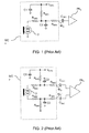
- Figures 1 and 2 show two known ways, single-ended and differential, respectively, to bias and connect the microphone circuit MC S , MC D to a preamplifier PA S , PAD using an RC network.
- the microphone circuit MC S , MC D comprises a microphone 3 and a biasing circuit R MB1 , R MB2 , R MB3 , C1, C2, fed by a bias voltage V BIAS .
- the DC bias voltage of the signal coming from the microphone circuit MC S , MC D at the output nodes M o , M o ' of the microphone circuit MC S , MC D will depend exclusively by the biasing circuit R MB1 , R MB2 , R MB3 , C1, C2 and is usually different from the DC bias input voltage of the preamplifier PA S , PAD.
- the level shifting between the microphone 3 and the preamplifier PA S , PAD DC biasing voltages is commonly obtained using a decoupling capacitor C DEC that produces, with the preamplifier PA S , PAD input resistance, a first order high-pass filter whose corner frequency is generally lower than 20Hz in order to avoid in-band audio signal perturbation.
- resistors R 1A and R 1B In the inverting case, due to noise generation, input resistors R 1A and R 1B cannot have high resistance values (typically from 10kOhm to 50kOhm), whereas in the non-inverting solution resistors R 3A and R 3B are used only to bias the amplifiers OA inputs at a common mode voltage V CM midway between ground and the supply voltage. Accordingly, resistors R 3A and R 3B don't contribute in noise generation and can be made with larger resistance values with respect to the inverting case (however, not more than some hundred of kOhms due to area occupation). In both cases, decoupling capacitors C DEC of more than 100nF are needed and such large capacitance values would be difficult to integrate in a chip.
- US 2002/0125949 discloses the above problem of the waste of area due to the integration in the chip of the decoupling capacitor C DEC , confirming that the integration of the decoupling capacitors C DEC is practicable only for relatively reduced capacitance values.
- US 7,899,196 addresses the problem of the area occupied by the preamplifier and discloses a digital microphone comprising a microphone element, a preamplifier with a high pass filter function an anti aliasing filter and an analog to digital converter.
- a microphone preamplifier circuit which is adapted to solve the above indicated problems concerning: the impossibility of reducing the PCB area occupation below a desired value due to the presence of one or more decoupling capacitors that cannot be integrated on a chip and the consumption of the preamplifier.
- a microphone preamplifier circuit adapted to be connected to a microphone circuit, the microphone circuit comprising a microphone and at least one output node.
- the microphone preamplifier circuit comprises a preamplifier comprising:
- Figure 5 shows a very schematic view of an embodiment of mobile terminal 5, such as for example a mobile phone 5, comprising a microphone circuit MC D .
- the microphone circuit MC D may be similar to the differential microphone circuit MC D represented in figure 2 .
- the microphone circuit MC D comprises a microphone 3, a microphone's biasing network and two differential output nodes M o , M o ' (represented in Figure 6 ).
- the microphone's biasing network may be identical or similar to the known biasing network of figure 2 .
- the mobile phone 5 comprises a circuit board 6 comprising a chip 7 comprising an integrated microphone preamplifier circuit 60.
- the circuit board 6 further comprises an analog to digital converter 70 and a digital audio processor 80.
- the preamplifier circuit 60, the digital converter 70 and the digital audio processor 80 are integrated on the same chip 7.
- a mobile terminal such for example a mobile phone
- a mobile terminal such for example a mobile phone
- microphone preamplifier circuit 60 can be also employed in systems and and/or devices different from a mobile terminal 5, for example in general in devices having audio communication and/or recording and/or processing capabilities such as, digital audio recorders, MP3 players, photo-cameras etc.
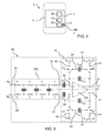
- Figure 6 shows an embodiment of microphone preamplifier circuit 60 comprising a preamplifier P A , the microphone preamplifier circuit 60 being adapted to be connected to the microphone 3, or more precisely to the microphone circuit MC D .
- the preamplifier P A is a differential preamplifier having two input nodes 10, 10' and an operational amplifier OA.
- the input nodes 10, 10' are adapted to be connected to the output nodes M o , M o ' of the microphone circuit MC D .
- the operational amplifier OA is arranged in said microphone preamplifier circuit 60 in order to operate in an inverting configuration.
- the structure of the microphone preamplifier circuit 60 and the preamplifier P A in the embodiment shown is totally symmetrical, in the present description mostly the upper branch of the preamplifier P A will be detailed, i.e. the branch above the ideal line L1. Moreover, it should be clear that even if in the present description a microphone preamplifier circuit 60 adapted to be connected to a differential microphone circuit M CD will be disclosed, the teachings of the present description can be easily extended by a man skilled in the field to the case in which the microphone preamplifier circuit is adapted to be connected to a single-ended microphone circuit.
- the preamplifier P A comprises an operational amplifier OA comprising at least one input 20,20' and at least one output 21, 21'. Moreover, the preamplifier P A comprises at least one input DC decoupling capacitor C D , C D , connected between the input node 10, 10' of the preamplifier P A and the input 20,20' of the operational amplifier OA.
- the preamplifier P A further comprises at least one feedback capacitor C 2A , C 2A ' connected between the input 20,20' and the output 21, 21' of the operational amplifier in order to set together with said input DC decoupling capacitor C D , C D ' a gain value G of the preamplifier circuit 60.
- the preamplifier P A comprises at least one first 40, 40' and at least one second feed node 41, 41' adapted to be fed by a first U CMIN and a second V CM bias voltage respectively.
- the preamplifier P A further comprises at least one switched capacitor C 2B , C 2B ' adapted to be selectively and alternatively connected under the control of a clock signal CK:
- the switched capacitor C 2B , C 2B' comprises:
- the second feed node 41,41' is configured to be fed with the common mode voltage V CM of the operational amplifier OA and the first feed node 40, 40' is configured to be fed with a further voltage V CMIN appropriate for input operation of the operational amplifier OA.
- V AL supply voltage
- the switched capacitor C 2B , C 2B ' is also adapted to discharge the feedback capacitor C 2A , C 2A ' ( Figure 6 ) at a given frequency than can be set to be relatively very low by selecting appropriate values for the frequency f CK of the clock signal CK and the appropriate capacitance values of the feedback C 2A , C 2A ' and the switched C 2B , C 2B ' capacitors.
- the preamplifier PA can be designed to be adapted to implement a high pass filtering function which, having a relatively very low high pass cut-off frequency, does not interfere with audio signals of interest for the operation of the microphone 3.
- said high pass filtering function has a high pass cut-off frequency of 6Hz or about 6Hz, for example comprised between 4 Hz and 8 Hz.
- the switched capacitor C 2B , C 2B has a capacitance value of about three magnitude orders lower the capacitance value of said feedback capacitor C 2A , C 2A' .
- the clock frequency f CK and the cutoff frequency represent a good compromise between area occupation and audio performance and represent a preferred choice, but it should be clear that a broad range of values is possible for both cut-off frequency and clock frequency. For example, paying in area the cutoff frequency can be much lower than 6Hz (e.g. 0,6 Hz), while paying in performance it can be much higher than 6Hz (e.g. 60 Hz).
- the DC decoupling capacitor C D , C D ' apart from contributing to the establishment of the gain G, only performs a DC decoupling function between the microphone circuit's output and the operational amplifier's and does not need to have a high value, as in the above described prior art circuits, in order to implement a high pass filtering function.
- the DC decoupling capacitor C D , C D ' can have a value of about 100pF and therefore it can be easily integrated without wasting a significant amount of silicon area.
- a microphone preamplifier circuit 60 as described above has the additional advantage of having a relatively reduced power consumption, due to the fact that no resistors are required for biasing and setting the gain of the preamplifier, since no physical feedback and biasing resistors are directly connected to the input 20,20' of the operational amplifier.
- the microphone preamplifier circuit 60 comprises an anti-aliasing filter INT C at the input of the preamplifier P A having an output terminal connected to the input node 10, 10' and an input terminal 61, 61' connected/connectable to the output node M o , M o ' of the microphone circuit M CD .
- the anti-aliasing filter INT C advantageously prevents the production of undesired replicas in the output signal of the preamplifier P A due to the presence of the switched capacitor C 2B , C 2B '.
- the anti-aliasing filter INT C is a passive filter comprising a plurality of RC ladder cells (in the differential embodiment, otherwise a plurality of RC serial cells in the single-ended embodiment).
- the anti-aliasing filter INT C comprises four RC ladder cells.
- the above described microphone preamplifier circuit 60 has the advantage of requiring one or more decoupling capacitors C D , C D ' having a relatively reduced capacitance value such that said capacitors can be integrated in the preamplifier's P A chip.
- the advantage in terms of area occupation is even greater when the preamplifier P A is shared between a plurality of n sources, such as for example n microphone circuits M CD , M CD 1 , M CD n .
- a multiplexer 50 for example, realized with CMOS transfer gates
- the decoupling capacitor C D ,C D ' in order to allow the selective connection among the different n sources and the preamplifier P A .
- a multiplexer 50 for example, realized with CMOS transfer gates
- only two relatively small decoupling capacitors C D are required instead of 2n external SMD capacitors, obtaining a large reduction in the area/space occupation.
Landscapes
- Engineering & Computer Science (AREA)
- Power Engineering (AREA)
- Microelectronics & Electronic Packaging (AREA)
- Multimedia (AREA)
- Physics & Mathematics (AREA)
- Acoustics & Sound (AREA)
- Signal Processing (AREA)
- Amplifiers (AREA)
Abstract
- at least one input node (10, 10') adapted to be connected to said output node (Mo, Mo');
- an operational amplifier (OA) comprising at least one input (20,20') and at least one output (21, 21');
- at least one input DC decoupling capacitor (CD, CD') connected between said input node (10, 10') and said first input of the operational amplifier (20,20');
- at least one feedback capacitor (C2A, C2A') connected between the input (20,20') and the output (21,'21) of the operational amplifier (OA) in order to set together with said input DC decoupling capacitor (CD, CD') a gain value of the preamplifier circuit (60);
- a first (40, 40') and a second feed node (41, 41') adapted to be fed by a first (VCIMIN) and a second (VCM) bias voltage respectively.
- between said input (20, 20') and said output (21, 21') of the operational amplifier (OA); and
- between said first (40, 40') and said second (41, 41') feed node.
Description
- The present disclosure relates to a microphone preamplifier circuit.
- One of the main aspects to take into account in the development of an electronic device, especially mobile devices, is the area occupation. In the field of mobile devices, such as mobile phones, the reduction of the area occupation on the Printed Circuit Board (PCB) is a key point in order to create phones with much more functionalities without altering their dimensions. The focus, during the years, has been to integrate inside a chip, where possible, all those passive components such as resistors, capacitors and inductors which represent the main limit for the area reduction. Inside old generation phones, such passive components were SMD (Surface Mount Devices) mounted directly on the main board. Later on, thanks to improvement in the technology, these devices were placed inside the chip package, a methodology known as PDI (Passive Device Integration), and in some cases directly integrated inside the chip. However, when it comes to the microphone preamplifying path the implementation of this approach has not been possible due to the huge capacitance value of the decoupling capacitors needed between the microphone and the preamplifier.
-
Figures 1 and 2 show two known ways, single-ended and differential, respectively, to bias and connect the microphone circuit MCS, MCD to a preamplifier PAS, PAD using an RC network. The microphone circuit MCS, MCD comprises amicrophone 3 and a biasing circuit RMB1, RMB2, RMB3, C1, C2, fed by a bias voltage VBIAS. - The DC bias voltage of the signal coming from the microphone circuit MCS, MCD at the output nodes Mo, Mo' of the microphone circuit MCS, MCD will depend exclusively by the biasing circuit RMB1, RMB2, RMB3, C1, C2 and is usually different from the DC bias input voltage of the preamplifier PAS, PAD. The level shifting between the
microphone 3 and the preamplifier PAS, PAD DC biasing voltages is commonly obtained using a decoupling capacitor CDEC that produces, with the preamplifier PAS, PAD input resistance, a first order high-pass filter whose corner frequency is generally lower than 20Hz in order to avoid in-band audio signal perturbation. - More detailed representations of the differential preamplifier PAD are shown in
Figure 3 (inverting configuration) andFigure 4 (non-inverting configuration). - In the inverting case, due to noise generation, input resistors R1A and R1B cannot have high resistance values (typically from 10kOhm to 50kOhm), whereas in the non-inverting solution resistors R3A and R3B are used only to bias the amplifiers OA inputs at a common mode voltage VCM midway between ground and the supply voltage. Accordingly, resistors R3A and R3B don't contribute in noise generation and can be made with larger resistance values with respect to the inverting case (however, not more than some hundred of kOhms due to area occupation). In both cases, decoupling capacitors CDEC of more than 100nF are needed and such large capacitance values would be difficult to integrate in a chip. In fact, with actual technologies on chip integration of a capacitor having such large capacitance value would require an area greater than 20mm2 and this fact made the integrating approach practically unusable.
US 2002/0125949 discloses the above problem of the waste of area due to the integration in the chip of the decoupling capacitor CDEC, confirming that the integration of the decoupling capacitors CDEC is practicable only for relatively reduced capacitance values. AlsoUS 7,899,196 addresses the problem of the area occupied by the preamplifier and discloses a digital microphone comprising a microphone element, a preamplifier with a high pass filter function an anti aliasing filter and an analog to digital converter. - Moreover, unfortunately, even with the PDI methodology the decoupling capacitors CDEC can't be realized because of their high capacitance value and the fact that none of their terminals are connected to a fixed potential. This is the reason why all the existing known solutions use SMD capacitors. Since a preamplifier usually has several inputs (voice microphone, mono and stereo audio microphone, mono and stereo line-in, etc.) and each one could be differential, it is clear that on a mobile phone's PCB there are many SMD decoupling capacitors CDEC.
- The presence of one or more SMD decoupling capacitors is clearly a bottle neck for the area reduction strategy, and there is a strong felt need of trying to find a solution to this problem, till now without success. The same above described problem holds for other consumer devices different from mobile phones, such as portable MP3 players, digital photo cameras, digital audio recorders, video cameras, and in general in devices with audio communication and/or recording and/or processing capabilities.
- Moreover, with reference to
figures 3 and 4 , a further problem of the prior art microphones preamplifiers, especially if they are intended to be embedded in mobile devices, is their power consumption. A significant contribution to such power consumption is given by the input and feedback resistors provided for setting the gain of the microphone preamplifier. - In view of the above described limitations of the prior art microphone preamplifier circuits, it is an object of the present invention to provide a microphone preamplifier circuit which is adapted to solve the above indicated problems concerning: the impossibility of reducing the PCB area occupation below a desired value due to the presence of one or more decoupling capacitors that cannot be integrated on a chip and the consumption of the preamplifier.
- The above object is reached by a microphone preamplifier circuit adapted to be connected to a microphone circuit, the microphone circuit comprising a microphone and at least one output node. The microphone preamplifier circuit comprises a preamplifier comprising:
- at least one input node adapted to be connected to said output node;
- an operational amplifier comprising at least one input and at least one output;
- at least one input DC decoupling capacitor connected between said input node of the operational amplifier and said input.
- between said input and said output of the operational amplifier; and
- between said first and said second node.
- Further features and advantages of the present invention will become more apparent from the following detailed description of exemplary but non-limiting embodiments thereof, as illustrated in the attached figures, in which:
-
Fig. 1 shows a schematic view of a first example of prior art microphone system comprising a microphone circuit and a preamplifier; -
Fig. 2 shows a schematic view of a second example of prior art microphone system comprising a microphone circuit and a preamplifier; -
Fig. 3 shows a schematic view of a first example of a known preamplifier for the microphone system offigure 2 ; -
Fig. 4 shows a schematic view of a second example of known preamplifier for the microphone system offigure 2 ; -
Fig. 5 shows a very schematic view of a device provided with audio recording and/or communication and/or processing capabilities; -
Fig. 6 shows an embodiment of a microphone preamplifier circuit; -
Fig. 7 shows a part of the circuit offigure 6 and the equivalent circuit thereof; and -
Fig. 8 shows an embodiment of a microphone system comprising the microphone preamplifier circuit offigure 6 . - In the attached figures identical or similar elements will be indicated with the same reference numbers/symbols.
-
Figure 5 shows a very schematic view of an embodiment ofmobile terminal 5, such as for example amobile phone 5, comprising a microphone circuit MCD. According to an embodiment, and without for this reason introducing any limitation, the microphone circuit MCD may be similar to the differential microphone circuit MCD represented infigure 2 . The microphone circuit MCD comprises amicrophone 3, a microphone's biasing network and two differential output nodes Mo, Mo' (represented inFigure 6 ). According to an embodiment, the microphone's biasing network may be identical or similar to the known biasing network offigure 2 . - The
mobile phone 5 comprises acircuit board 6 comprising achip 7 comprising an integratedmicrophone preamplifier circuit 60. According to the embodiment shown, thecircuit board 6 further comprises an analog todigital converter 70 and adigital audio processor 80. In the example offigure 5 , thepreamplifier circuit 60, thedigital converter 70 and thedigital audio processor 80 are integrated on thesame chip 7. - As the general structure and the operation of a mobile terminal, such for example a mobile phone, are well known to a man skilled in the field, for sake of conciseness they will not be detailed further in the following part of the description. On the contrary, the following part of the description will be mainly focused on the
microphone preamplifier circuit 60. It is important to remark that suchmicrophone preamplifier circuit 60 can be also employed in systems and and/or devices different from amobile terminal 5, for example in general in devices having audio communication and/or recording and/or processing capabilities such as, digital audio recorders, MP3 players, photo-cameras etc. -
Figure 6 shows an embodiment ofmicrophone preamplifier circuit 60 comprising a preamplifier PA, themicrophone preamplifier circuit 60 being adapted to be connected to themicrophone 3, or more precisely to the microphone circuit MCD. - According to the embodiment shown, the preamplifier PA is a differential preamplifier having two
input nodes 10, 10' and an operational amplifier OA. Theinput nodes 10, 10' are adapted to be connected to the output nodes Mo, Mo' of the microphone circuit MCD. In the particular example shown infigure 6 , the operational amplifier OA is arranged in saidmicrophone preamplifier circuit 60 in order to operate in an inverting configuration. - Since the structure of the
microphone preamplifier circuit 60 and the preamplifier PA in the embodiment shown is totally symmetrical, in the present description mostly the upper branch of the preamplifier PA will be detailed, i.e. the branch above the ideal line L1. Moreover, it should be clear that even if in the present description amicrophone preamplifier circuit 60 adapted to be connected to a differential microphone circuit MCD will be disclosed, the teachings of the present description can be easily extended by a man skilled in the field to the case in which the microphone preamplifier circuit is adapted to be connected to a single-ended microphone circuit. - With reference to
figure 6 , the preamplifier PA comprises an operational amplifier OA comprising at least oneinput 20,20' and at least oneoutput 21, 21'. Moreover, the preamplifier PA comprises at least one input DC decoupling capacitor CD, CD, connected between theinput node 10, 10' of the preamplifier PA and theinput 20,20' of the operational amplifier OA. - The preamplifier PA further comprises at least one feedback capacitor C2A, C2A' connected between the
input 20,20' and theoutput 21, 21' of the operational amplifier in order to set together with said input DC decoupling capacitor CD, CD' a gain value G of thepreamplifier circuit 60. Such gain value G is given by:
- As shown in
figure 6 , the preamplifier PA comprises at least one first 40, 40' and at least onesecond feed node 41, 41' adapted to be fed by a first UCMIN and a second VCM bias voltage respectively. - The preamplifier PA further comprises at least one switched capacitor C2B, C2B' adapted to be selectively and alternatively connected under the control of a clock signal CK:
- between the
input 20, 20' and theoutput 21, 21' of the preamplifier PA, i.e. in parallel to the feedback capacitor C2A, C2A' ; and - between the above mentioned first 40, 40' and second 41, 41' feed nodes.
- According to an embodiment, the switched capacitor C2B, C2B' comprises:
- a first plate (in
figure 6 on the left side of capacitor C2B, C2B') adapted to be selectively and alternatively connected to theinput 20, 20' and thefirst feed node 40,40'; and - a second plate (in
figure 6 on the right side of capacitor C2B, C2B') adapted to be selectively and alternatively connected to theoutput 21, 21' and thesecond feed node 41, 41'. - According to the above embodiment the
second feed node 41,41' is configured to be fed with the common mode voltage VCM of the operational amplifier OA and thefirst feed node 40, 40' is configured to be fed with a further voltage VCMIN appropriate for input operation of the operational amplifier OA. For example, if the operational amplifier OA is fed with a supply voltage VAL: - the common mode voltage VCM is half of said supply voltage VAL;
- the above mentioned further voltage VCMIN is lower than said common mode voltage VCM if the operational amplifier OA has P-type input and higher than said common voltage VCM if the operational amplifier OA has N-type input.
- From the above description it is therefore clear that the switched capacitor C2B, C2B' is a capacitor provided to bias the
input 20,20' of the operational amplifier OA to the further voltage VCMIN, since as shown infigure 7 it can be modeled with a resistor having an equivalent resistance REQ = 1/(fCK·C2B) in series with a battery providing a voltage VBAT = VCM-VCMIN. - From
Fig.7 it is therefore clear that the switched capacitor C2B, C2B' is also adapted to discharge the feedback capacitor C2A, C2A' (Figure 6 ) at a given frequency than can be set to be relatively very low by selecting appropriate values for the frequency fCK of the clock signal CK and the appropriate capacitance values of the feedback C2A, C2A' and the switched C2B, C2B' capacitors. By selecting the above indicated appropriated values, the preamplifier PA can be designed to be adapted to implement a high pass filtering function which, having a relatively very low high pass cut-off frequency, does not interfere with audio signals of interest for the operation of themicrophone 3. According to an embodiment, said high pass filtering function has a high pass cut-off frequency of 6Hz or about 6Hz, for example comprised between 4 Hz and 8 Hz. - The time constant of the above mentioned high pass filtering is given by:

- In view of the above, the high pass cut-off frequency can be made as to have a value of about 6 Hz if for example the clock frequency fCK has a value of the order of magnitude of 100 kHz, for example fCK = 100 kHz and the switched capacitor C2B, C2B' has a capacitance value significantly lower than a capacitance value of the feedback capacitor C2A, C2A'. For example, the switched capacitor C2B, C2B, has a capacitance value of about three magnitude orders lower the capacitance value of said feedback capacitor C2A, C2A'. In a practical embodiment, a high pass cut-off frequency of about 6 Hz can be for example obtained if fCK = 100 KHz, C2A=100pF, C2A=1/30 pF.
- The above values for the clock frequency fCK and the cutoff frequency represent a good compromise between area occupation and audio performance and represent a preferred choice, but it should be clear that a broad range of values is possible for both cut-off frequency and clock frequency. For example, paying in area the cutoff frequency can be much lower than 6Hz (e.g. 0,6 Hz), while paying in performance it can be much higher than 6Hz (e.g. 60 Hz).
- It is clear that the above condition (1) fixes the limit for the minimum value of the capacitor C2A and in turn of C2B. In any case it is clear from the example above that such values can be easily integrated without wasting a significant amount of silicon area.
- Moreover, it is to be noticed that since the high pass filtering function is performed by the operational amplifier OA, the feedback capacitor C2A, C2A' and the switched capacitor C2B, C2B', the DC decoupling capacitor CD, CD', apart from contributing to the establishment of the gain G, only performs a DC decoupling function between the microphone circuit's output and the operational amplifier's and does not need to have a high value, as in the above described prior art circuits, in order to implement a high pass filtering function. For example, the DC decoupling capacitor CD, CD' can have a value of about 100pF and therefore it can be easily integrated without wasting a significant amount of silicon area.
- Moreover, a
microphone preamplifier circuit 60 as described above has the additional advantage of having a relatively reduced power consumption, due to the fact that no resistors are required for biasing and setting the gain of the preamplifier, since no physical feedback and biasing resistors are directly connected to theinput 20,20' of the operational amplifier. - As shown in
figure 6 , according to an embodiment, themicrophone preamplifier circuit 60 comprises an anti-aliasing filter INTC at the input of the preamplifier PA having an output terminal connected to theinput node 10, 10' and aninput terminal 61, 61' connected/connectable to the output node Mo, Mo' of the microphone circuit MCD. The anti-aliasing filter INTC advantageously prevents the production of undesired replicas in the output signal of the preamplifier PA due to the presence of the switched capacitor C2B, C2B'. - According to an embodiment, the anti-aliasing filter INTC is a passive filter comprising a plurality of RC ladder cells (in the differential embodiment, otherwise a plurality of RC serial cells in the single-ended embodiment). In the particular example shown the anti-aliasing filter INTC comprises four RC ladder cells.
- As is clear from the above description, the above described
microphone preamplifier circuit 60 has the advantage of requiring one or more decoupling capacitors CD, CD' having a relatively reduced capacitance value such that said capacitors can be integrated in the preamplifier's PA chip. The advantage in terms of area occupation is even greater when the preamplifier PA is shared between a plurality of n sources, such as for example n microphone circuits MCD, MCD 1, MCD n. In this case, as shown infigure 8 , it is possible to place, or better to integrate, a multiplexer 50 (for example, realized with CMOS transfer gates) just before the decoupling capacitor CD ,CD' in order to allow the selective connection among the different n sources and the preamplifier PA. In this case, only two relatively small decoupling capacitors CD (if the architecture of the preamplifier is differential) are required instead of 2n external SMD capacitors, obtaining a large reduction in the area/space occupation. - Naturally, in order to satisfy contingent and specific requirements, a person skilled in the art may apply to the above-described microphone preamplifier circuits many modifications and variations, all of which, however, are included within the scope of protection of the invention as defined by the following claims.
Claims (16)
- Microphone preamplifier circuit (60) adapted to be connected to a microphone circuit (MCD), the microphone circuit (MCD) comprising a microphone (3) and at least one output node (Mo, Mo'), the microphone preamplifier circuit (60) comprising a preamplifier (PA) comprising:- at least one input node (10, 10') adapted to be connected to said output node (Mo, Mo');- an operational amplifier (OA) comprising at least one input (20,20') and at least one output (21, 21');- at least one input DC decoupling capacitor (CD, CD') connected between said input node (10, 10') and said first input (20,20') of the operational amplifier;- at least one feedback capacitor (C2A, C2A') connected between the input (20,20') and the output (21,'21) of the operational amplifier (OA) in order to set together with said input DC decoupling capacitor (CD, CD,) a gain value of the preamplifier circuit (60);- a first (40, 40') and a second feed node (41, 41') adapted to be fed by a first (VCIMIN) and a second (VCM) bias voltage respectively;wherein said preamplifier further comprises at least one switched capacitor (C2B, C2B') adapted to be selectively and alternatively connected under the control of a clock signal (CK):- between said input (20, 20') and said output (21, 21') of the operational amplifier (OA); and- between said first (40, 40') and said second (41, 41') feed node.
- Microphone preamplifier circuit (60) according to claim 1, wherein said switched capacitor (C2B, C2B') comprises:- a first plate adapted to be selectively connected to said input of the operational amplifier (20, 20') and said first feed node (40,40'); and- a second plate adapted to be selectively connected to said output of the operational amplifier (21, 21') and said second feed node (41, 41');and wherein said second feed node (41,41') is configured to be fed with the common mode voltage (VCM) of said operational amplifier (OA) and said first feed node (40, 40') is configured to be fed with a further voltage (VCMIN) appropriate for input operation of said operational amplifier (OA).
- Microphone preamplifier circuit (60) according to claim 1, wherein said operational amplifier (OA) is fed with a supply voltage (VAL) and wherein:- said common mode voltage (VCM) is half of said supply voltage (VAL) ;- said further voltage (VCMIN) is lower than said common mode voltage (VCM) if the operational amplifier (OA) has a P-type input and higher than said common voltage (VCM) if the operational amplifier has a N-type input.
- Microphone preamplifier circuit (60) according to any one of the previous claims, wherein said clock signal (CK) has a frequency such that said switched capacitor (C2B, C2B') is adapted to discharge said feedback capacitor (C2A, C2A') at a relatively low frequency so that the preamplifier (PA) is adapted to implement a high pass filtering function which does not interfere with audio signals of interest for the operation of said microphone (3).
- Microphone preamplifier circuit (60) according to claim 4, wherein said high pass filtering function has a high pass cut-off frequency of 6Hz or about 6Hz.
- Microphone preamplifier circuit (60) according to claims 4 or 5, wherein said clock signal (CK) has a frequency of the order of magnitude of 100 kHz.
- Microphone preamplifier circuit (60) according to any one of the previous claims, wherein said switched capacitor (C2B, C2B') has a capacitance value significantly lower than a capacitance value of said feedback capacitor (C2A, C2A').
- Microphone preamplifier circuit according to claim 7, wherein said switched capacitor (C2B, C2B') has a capacitance value of about three magnitude orders lower the capacitance value of said feedback capacitor (C2A, C2A').
- Microphone preamplifier circuit (60) according to any one of the previous claims, wherein the operational amplifier (OA) is a differential amplifier, said preamplifier circuit (60) having a symmetrical circuital structure having two of said input DC decoupling capacitors (CD, CD,), two of said feedback capacitors (C2A, C2A') and two of said switched capacitors (C2B, C2B').
- Microphone preamplifier circuit (60) according to any one of the previous claims, wherein said operational amplifier (OA) is arranged in said microphone preamplifier circuit (60) in order to operate in an inverting configuration.
- Microphone preamplifier circuit (60) according to any one of the previous claims, comprising an anti-aliasing filter (INTC) having an output terminal connected to said input node (10, 10') and an input terminal (61, 61') connected/connectable to said output node (Mo, Mo') of the microphone circuit (MCD).
- Microphone preamplifier circuit (60) according to claim 11, wherein said anti-aliasing filter (INTC) comprises a plurality of RC ladder, or serial, cells.
- Microphone preamplifier circuit (60) according to any of the previous claims, comprising a multiplexer (50) adapted to selectively connect said input node (10, 10') to one of a plurality of microphone circuits.
- Microphone preamplifier circuit (60) according to claims 12 and 13, wherein said multiplexer (50), said anti-aliasing filter (INTC), said input decoupling capacitor (CD, CD') and said preamplifier (PA) are integrated in a same chip (7).
- Microphone system (60, MCD) comprising at least a microphone circuit (MCD) and the microphone preamplifier circuit (60) according to any one of the previous claims.
- Device (5) provided with audio processing and/or recording and/or communication capabilities, comprising the microphone system (60, MCD) according to claim 15.
Priority Applications (3)
| Application Number | Priority Date | Filing Date | Title |
|---|---|---|---|
| EP11175387A EP2552018A1 (en) | 2011-07-26 | 2011-07-26 | Microphone preamplifier circuit |
| PCT/EP2012/063826 WO2013014009A1 (en) | 2011-07-26 | 2012-07-13 | Microphone preamplifier circuit |
| US14/129,320 US9554209B2 (en) | 2011-07-26 | 2012-07-13 | Microphone preamplifier circuit |
Applications Claiming Priority (1)
| Application Number | Priority Date | Filing Date | Title |
|---|---|---|---|
| EP11175387A EP2552018A1 (en) | 2011-07-26 | 2011-07-26 | Microphone preamplifier circuit |
Publications (1)
| Publication Number | Publication Date |
|---|---|
| EP2552018A1 true EP2552018A1 (en) | 2013-01-30 |
Family
ID=45024116
Family Applications (1)
| Application Number | Title | Priority Date | Filing Date |
|---|---|---|---|
| EP11175387A Withdrawn EP2552018A1 (en) | 2011-07-26 | 2011-07-26 | Microphone preamplifier circuit |
Country Status (3)
| Country | Link |
|---|---|
| US (1) | US9554209B2 (en) |
| EP (1) | EP2552018A1 (en) |
| WO (1) | WO2013014009A1 (en) |
Families Citing this family (6)
| Publication number | Priority date | Publication date | Assignee | Title |
|---|---|---|---|---|
| US9502019B2 (en) * | 2014-02-10 | 2016-11-22 | Robert Bosch Gmbh | Elimination of 3D parasitic effects on microphone power supply rejection |
| EP3151425A1 (en) | 2015-09-30 | 2017-04-05 | Nawrocki, Piotr | Electronic preamplifier system |
| US10292278B2 (en) * | 2017-08-21 | 2019-05-14 | Seagate Technology Llc | Compact printed circuit board assembly with insulating endcap via |
| DE212018000392U1 (en) * | 2018-01-04 | 2020-08-05 | Knowles Electronics, Llc | Pressure sensor microphone device |
| CN109275071B (en) * | 2018-11-06 | 2022-03-04 | 珠海市杰理科技股份有限公司 | Audio processing device, chip, system and method |
| WO2021006816A1 (en) * | 2019-07-08 | 2021-01-14 | Creative Technology Ltd. | Method to reduce noise in microphone circuits |
Citations (6)
| Publication number | Priority date | Publication date | Assignee | Title |
|---|---|---|---|---|
| EP0375017A2 (en) * | 1988-12-22 | 1990-06-27 | STMicroelectronics S.r.l. | Completely differential filter with switched condensers using CMOS operational amplifiers with no common-mode feedback |
| US20020125949A1 (en) | 2001-03-09 | 2002-09-12 | Stenberg Lars J. | Electret condensor microphone preamplifier that is insensitive to leakage currents at the input |
| US6556072B1 (en) * | 1994-04-21 | 2003-04-29 | Stmicroelectronics S.R.L. | Low distortion circuit with switched capacitors |
| EP2133993A1 (en) * | 2008-06-13 | 2009-12-16 | Sicon Semiconductor AB | Gain circuit |
| US7899196B2 (en) | 2004-02-09 | 2011-03-01 | Audioasics A/S | Digital microphone |
| US20110140945A1 (en) * | 2009-12-11 | 2011-06-16 | Zoran Corporation | Gain circuit |
Family Cites Families (3)
| Publication number | Priority date | Publication date | Assignee | Title |
|---|---|---|---|---|
| JP3904789B2 (en) | 2000-01-28 | 2007-04-11 | 本田技研工業株式会社 | Chain transmission |
| US8085954B2 (en) * | 2005-07-21 | 2011-12-27 | Freescale Semiconductor, Inc. | Microphone amplification arrangement and integrated circuit therefor |
| IT1392309B1 (en) * | 2008-12-15 | 2012-02-24 | St Microelectronics Srl | INTEGRATED CIRCUIT BUILDING AMPLIFICATION CIRCUIT AND SYSTEM INCLUDING THE CIRCUIT |
-
2011
- 2011-07-26 EP EP11175387A patent/EP2552018A1/en not_active Withdrawn
-
2012
- 2012-07-13 WO PCT/EP2012/063826 patent/WO2013014009A1/en active Application Filing
- 2012-07-13 US US14/129,320 patent/US9554209B2/en not_active Expired - Fee Related
Patent Citations (6)
| Publication number | Priority date | Publication date | Assignee | Title |
|---|---|---|---|---|
| EP0375017A2 (en) * | 1988-12-22 | 1990-06-27 | STMicroelectronics S.r.l. | Completely differential filter with switched condensers using CMOS operational amplifiers with no common-mode feedback |
| US6556072B1 (en) * | 1994-04-21 | 2003-04-29 | Stmicroelectronics S.R.L. | Low distortion circuit with switched capacitors |
| US20020125949A1 (en) | 2001-03-09 | 2002-09-12 | Stenberg Lars J. | Electret condensor microphone preamplifier that is insensitive to leakage currents at the input |
| US7899196B2 (en) | 2004-02-09 | 2011-03-01 | Audioasics A/S | Digital microphone |
| EP2133993A1 (en) * | 2008-06-13 | 2009-12-16 | Sicon Semiconductor AB | Gain circuit |
| US20110140945A1 (en) * | 2009-12-11 | 2011-06-16 | Zoran Corporation | Gain circuit |
Also Published As
| Publication number | Publication date |
|---|---|
| US20140153746A1 (en) | 2014-06-05 |
| US9554209B2 (en) | 2017-01-24 |
| WO2013014009A1 (en) | 2013-01-31 |
Similar Documents
| Publication | Publication Date | Title |
|---|---|---|
| US9288573B2 (en) | Interface circuit for connecting a microphone circuit to a preamplifier | |
| US9554209B2 (en) | Microphone preamplifier circuit | |
| EP2834993B1 (en) | Headset switches with crosstalk reduction | |
| US8059837B2 (en) | Audio processing method and system | |
| US8335328B2 (en) | Programmable integrated microphone interface circuit | |
| EP2312813A1 (en) | Circuit apparatus for recognizing earphone in mobile terminal | |
| CN103580633B (en) | Semiconductor integrated circuit and the radio telecommunication terminal including the semiconductor integrated circuit | |
| US20080310655A1 (en) | Programmable integrated microphone interface circuit | |
| CN103796134A (en) | System and method for capacitive signal source amplifier | |
| JP2017510206A (en) | Multistage switched capacitor DC blocking circuit for audio front end | |
| US9590579B2 (en) | Wide range transimpedance amplifier | |
| CN107993628B (en) | Common voltage compensation circuit, compensation method thereof, display panel and display device | |
| US20150181335A1 (en) | System and Method for a Cancelation Circuit | |
| EP2319232B1 (en) | Method for driving a ground reference on a signal path, control circuit for driving a ground reference on a signal path, and mobile device | |
| US9054646B2 (en) | Integrated amplifier for driving acoustic transducers | |
| CN104284289A (en) | System and Method for a Microphone Amplifier | |
| US7868688B2 (en) | Leakage independent very low bandwith current filter | |
| EP1762023B1 (en) | Passive processing device for interfacing and for esd and radio signal rejection in audio signal paths of an electronic device | |
| US20120250898A1 (en) | Processing Chip for a Digital Microphone and related Input Circuit and a Digital Microphone | |
| CN104053094B (en) | A kind of active rejector circuit | |
| WO2022117548A1 (en) | Audio processing device and method for amplification of an audio signal | |
| EP2461604B1 (en) | Differential microphone circuit | |
| CN104581598A (en) | System and Method for Transducer Interface | |
| US6700445B2 (en) | Filter circuits based on trans-conductor circuits | |
| ATE486310T1 (en) | DEVICE FOR FILTERING A REFERENCE VOLTAGE AND MOBILE PHONES COMPRISING THIS DEVICE |
Legal Events
| Date | Code | Title | Description |
|---|---|---|---|
| PUAI | Public reference made under article 153(3) epc to a published international application that has entered the european phase |
Free format text: ORIGINAL CODE: 0009012 |
|
| AK | Designated contracting states |
Kind code of ref document: A1 Designated state(s): AL AT BE BG CH CY CZ DE DK EE ES FI FR GB GR HR HU IE IS IT LI LT LU LV MC MK MT NL NO PL PT RO RS SE SI SK SM TR |
|
| AX | Request for extension of the european patent |
Extension state: BA ME |
|
| 17P | Request for examination filed |
Effective date: 20130729 |
|
| RBV | Designated contracting states (corrected) |
Designated state(s): AL AT BE BG CH CY CZ DE DK EE ES FI FR GB GR HR HU IE IS IT LI LT LU LV MC MK MT NL NO PL PT RO RS SE SI SK SM TR |
|
| RAP1 | Party data changed (applicant data changed or rights of an application transferred) |
Owner name: OCT CIRCUIT TECHNOLOGIES INTERNATIONAL LIMITED |
|
| STAA | Information on the status of an ep patent application or granted ep patent |
Free format text: STATUS: THE APPLICATION HAS BEEN WITHDRAWN |
|
| 18W | Application withdrawn |
Effective date: 20180307 |