EP2833413A2 - Photovoltaische Zelle aus Verbindungshalbleiter - Google Patents
Photovoltaische Zelle aus Verbindungshalbleiter Download PDFInfo
- Publication number
- EP2833413A2 EP2833413A2 EP14178623.6A EP14178623A EP2833413A2 EP 2833413 A2 EP2833413 A2 EP 2833413A2 EP 14178623 A EP14178623 A EP 14178623A EP 2833413 A2 EP2833413 A2 EP 2833413A2
- Authority
- EP
- European Patent Office
- Prior art keywords
- layer
- type
- cell
- inp
- photoelectric conversion
- Prior art date
- Legal status (The legal status is an assumption and is not a legal conclusion. Google has not performed a legal analysis and makes no representation as to the accuracy of the status listed.)
- Withdrawn
Links
Images






Classifications
-
- H—ELECTRICITY
- H10—SEMICONDUCTOR DEVICES; ELECTRIC SOLID-STATE DEVICES NOT OTHERWISE PROVIDED FOR
- H10F—INORGANIC SEMICONDUCTOR DEVICES SENSITIVE TO INFRARED RADIATION, LIGHT, ELECTROMAGNETIC RADIATION OF SHORTER WAVELENGTH OR CORPUSCULAR RADIATION
- H10F10/00—Individual photovoltaic cells, e.g. solar cells
- H10F10/10—Individual photovoltaic cells, e.g. solar cells having potential barriers
-
- H—ELECTRICITY
- H10—SEMICONDUCTOR DEVICES; ELECTRIC SOLID-STATE DEVICES NOT OTHERWISE PROVIDED FOR
- H10F—INORGANIC SEMICONDUCTOR DEVICES SENSITIVE TO INFRARED RADIATION, LIGHT, ELECTROMAGNETIC RADIATION OF SHORTER WAVELENGTH OR CORPUSCULAR RADIATION
- H10F10/00—Individual photovoltaic cells, e.g. solar cells
- H10F10/10—Individual photovoltaic cells, e.g. solar cells having potential barriers
- H10F10/16—Photovoltaic cells having only PN heterojunction potential barriers
- H10F10/161—Photovoltaic cells having only PN heterojunction potential barriers comprising multiple PN heterojunctions, e.g. tandem cells
-
- H—ELECTRICITY
- H10—SEMICONDUCTOR DEVICES; ELECTRIC SOLID-STATE DEVICES NOT OTHERWISE PROVIDED FOR
- H10F—INORGANIC SEMICONDUCTOR DEVICES SENSITIVE TO INFRARED RADIATION, LIGHT, ELECTROMAGNETIC RADIATION OF SHORTER WAVELENGTH OR CORPUSCULAR RADIATION
- H10F10/00—Individual photovoltaic cells, e.g. solar cells
- H10F10/10—Individual photovoltaic cells, e.g. solar cells having potential barriers
- H10F10/14—Photovoltaic cells having only PN homojunction potential barriers
- H10F10/142—Photovoltaic cells having only PN homojunction potential barriers comprising multiple PN homojunctions, e.g. tandem cells
-
- H—ELECTRICITY
- H10—SEMICONDUCTOR DEVICES; ELECTRIC SOLID-STATE DEVICES NOT OTHERWISE PROVIDED FOR
- H10F—INORGANIC SEMICONDUCTOR DEVICES SENSITIVE TO INFRARED RADIATION, LIGHT, ELECTROMAGNETIC RADIATION OF SHORTER WAVELENGTH OR CORPUSCULAR RADIATION
- H10F10/00—Individual photovoltaic cells, e.g. solar cells
- H10F10/10—Individual photovoltaic cells, e.g. solar cells having potential barriers
- H10F10/14—Photovoltaic cells having only PN homojunction potential barriers
- H10F10/144—Photovoltaic cells having only PN homojunction potential barriers comprising only Group III-V materials, e.g. GaAs,AlGaAs, or InP photovoltaic cells
-
- H—ELECTRICITY
- H10—SEMICONDUCTOR DEVICES; ELECTRIC SOLID-STATE DEVICES NOT OTHERWISE PROVIDED FOR
- H10F—INORGANIC SEMICONDUCTOR DEVICES SENSITIVE TO INFRARED RADIATION, LIGHT, ELECTROMAGNETIC RADIATION OF SHORTER WAVELENGTH OR CORPUSCULAR RADIATION
- H10F10/00—Individual photovoltaic cells, e.g. solar cells
- H10F10/10—Individual photovoltaic cells, e.g. solar cells having potential barriers
- H10F10/16—Photovoltaic cells having only PN heterojunction potential barriers
- H10F10/163—Photovoltaic cells having only PN heterojunction potential barriers comprising only Group III-V materials, e.g. GaAs/AlGaAs or InP/GaInAs photovoltaic cells
-
- H—ELECTRICITY
- H10—SEMICONDUCTOR DEVICES; ELECTRIC SOLID-STATE DEVICES NOT OTHERWISE PROVIDED FOR
- H10F—INORGANIC SEMICONDUCTOR DEVICES SENSITIVE TO INFRARED RADIATION, LIGHT, ELECTROMAGNETIC RADIATION OF SHORTER WAVELENGTH OR CORPUSCULAR RADIATION
- H10F19/00—Integrated devices, or assemblies of multiple devices, comprising at least one photovoltaic cell covered by group H10F10/00, e.g. photovoltaic modules
- H10F19/90—Structures for connecting between photovoltaic cells, e.g. interconnections or insulating spacers
- H10F19/902—Structures for connecting between photovoltaic cells, e.g. interconnections or insulating spacers for series or parallel connection of photovoltaic cells
- H10F19/906—Structures for connecting between photovoltaic cells, e.g. interconnections or insulating spacers for series or parallel connection of photovoltaic cells characterised by the materials of the structures
-
- H—ELECTRICITY
- H10—SEMICONDUCTOR DEVICES; ELECTRIC SOLID-STATE DEVICES NOT OTHERWISE PROVIDED FOR
- H10F—INORGANIC SEMICONDUCTOR DEVICES SENSITIVE TO INFRARED RADIATION, LIGHT, ELECTROMAGNETIC RADIATION OF SHORTER WAVELENGTH OR CORPUSCULAR RADIATION
- H10F71/00—Manufacture or treatment of devices covered by this subclass
-
- H—ELECTRICITY
- H10—SEMICONDUCTOR DEVICES; ELECTRIC SOLID-STATE DEVICES NOT OTHERWISE PROVIDED FOR
- H10F—INORGANIC SEMICONDUCTOR DEVICES SENSITIVE TO INFRARED RADIATION, LIGHT, ELECTROMAGNETIC RADIATION OF SHORTER WAVELENGTH OR CORPUSCULAR RADIATION
- H10F71/00—Manufacture or treatment of devices covered by this subclass
- H10F71/127—The active layers comprising only Group III-V materials, e.g. GaAs or InP
- H10F71/1272—The active layers comprising only Group III-V materials, e.g. GaAs or InP comprising at least three elements, e.g. GaAlAs or InGaAsP
-
- H—ELECTRICITY
- H10—SEMICONDUCTOR DEVICES; ELECTRIC SOLID-STATE DEVICES NOT OTHERWISE PROVIDED FOR
- H10F—INORGANIC SEMICONDUCTOR DEVICES SENSITIVE TO INFRARED RADIATION, LIGHT, ELECTROMAGNETIC RADIATION OF SHORTER WAVELENGTH OR CORPUSCULAR RADIATION
- H10F77/00—Constructional details of devices covered by this subclass
- H10F77/10—Semiconductor bodies
- H10F77/12—Active materials
- H10F77/123—Active materials comprising only Group II-VI materials, e.g. CdS, ZnS or HgCdTe
- H10F77/1237—Active materials comprising only Group II-VI materials, e.g. CdS, ZnS or HgCdTe having at least three elements, e.g. HgCdTe
-
- H—ELECTRICITY
- H10—SEMICONDUCTOR DEVICES; ELECTRIC SOLID-STATE DEVICES NOT OTHERWISE PROVIDED FOR
- H10F—INORGANIC SEMICONDUCTOR DEVICES SENSITIVE TO INFRARED RADIATION, LIGHT, ELECTROMAGNETIC RADIATION OF SHORTER WAVELENGTH OR CORPUSCULAR RADIATION
- H10F77/00—Constructional details of devices covered by this subclass
- H10F77/10—Semiconductor bodies
- H10F77/12—Active materials
- H10F77/124—Active materials comprising only Group III-V materials, e.g. GaAs
- H10F77/1248—Active materials comprising only Group III-V materials, e.g. GaAs having three or more elements, e.g. GaAlAs, InGaAs or InGaAsP
-
- Y—GENERAL TAGGING OF NEW TECHNOLOGICAL DEVELOPMENTS; GENERAL TAGGING OF CROSS-SECTIONAL TECHNOLOGIES SPANNING OVER SEVERAL SECTIONS OF THE IPC; TECHNICAL SUBJECTS COVERED BY FORMER USPC CROSS-REFERENCE ART COLLECTIONS [XRACs] AND DIGESTS
- Y02—TECHNOLOGIES OR APPLICATIONS FOR MITIGATION OR ADAPTATION AGAINST CLIMATE CHANGE
- Y02E—REDUCTION OF GREENHOUSE GAS [GHG] EMISSIONS, RELATED TO ENERGY GENERATION, TRANSMISSION OR DISTRIBUTION
- Y02E10/00—Energy generation through renewable energy sources
- Y02E10/50—Photovoltaic [PV] energy
- Y02E10/544—Solar cells from Group III-V materials
Definitions
- the present invention relates to a compound photovoltaic cell.
- a concentrated photovoltaic cell which utilizes an inexpensive condensing lens or mirrors in order to condense the sunlight and converts the condensed sunlight into electric energy has been known.
- a band gap of a compound photovoltaic cell can be varied by controlling a composition ratio of compound semiconductor materials with relative ease. Therefore, studies are being conducted to improve energy conversion efficiency of the compound photovoltaic cell by absorbing the sunlight in a broader wavelength range.
- photovoltaic cell formed by depositing a GaInP cell and a GaAs cell that are lattice-matched with GaAs onto a GaAs substrate and by depositing a GaInAs cell which has about 2% lattice mismatch with GaAs onto the GaInP cell and the GaAs cell via a lattice relaxation buffer layer, for the sake of improving the conversion efficiency (see, for example, Non-Patent Document 1).
- a photovoltaic cell formed by forming a GaInP top cell and a highly-doped p + -type layer onto a GaAs substrate, by forming a GaInAs bottom cell and a highly-doped n + -type layer onto an InP substrate, and by joining (bonding) the p + -type layer and the n + -type layer in order to form a tunnel junction layer.
- the GaInP top cell and the GaInAs bottom cell are bonded in series with each other via the tunnel junction layer (see, for example, Patent Document 1).
- Patent Document 1 US 2012/0138116
- Non-patent Document 1 Proceedings of the 29th IEEE Photovoltaic Specialists Conference (2010) pp.412-417 .
- the present invention has been made in view of the above-described problems, and it is an object of at least one embodiment of the present invention to provide a compound photovoltaic cell with an improved conversion efficiency.
- An aspect of the present invention provides a compound photovoltaic cell which includes a first substrate, one or more first photoelectric conversion cells configured to be made of a first compound semiconductor material and to be formed on the first substrate, a tunnel junction layer formed on the one or more first photoelectric conversion cells, and one or more second photoelectric conversion cells configured to be made of a second compound semiconductor material which is lattice mismatched with a material of the first substrate, to be connected to the one or more first photoelectric conversion cells via the tunnel junction layer, and to be disposed on an incident side in a light incident direction with respect to the one or more first photoelectric conversion cells, wherein band gaps of the one or more first photoelectric conversion cells and the one or more second photoelectric conversion cells become smaller from an incident side to a back side in a light incident direction, and wherein the tunnel junction layer includes a p-type layer disposed on the incident side and a n-type layer disposed on the back side, the p-type layer being a p + -type (Al)GaInAs layer
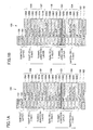
- FIGS. 1A, 1B and 2 are diagrams illustrating cross sections of a compound photovoltaic cell 100 according to the first embodiment.
- the compound photovoltaic cell 100 includes an electrode 101, an electrode 102, an InP substrate 103, a GaInPAs cell 104, a tunnel junction layer 105, a GaAs cell 106, a tunnel junction layer 107, a GaInP cell 108 and a contact layer 109.
- the tunnel junction layer 105 is formed between the GaInPAs cell 104 and the GaAs cell 106.
- the tunnel junction layer 107 is formed between the GaAs cell 106 and the GaInP cell 108.
- the GaInPAs cell 104, the GaAs cell 106 and the GaInP cell 108 are electrically and optically connected in series with each other by being bonded by the tunnel junction layers 105 and 107.
- each of the GaInPAs cell 104, the GaAs cell 106 and the GaInP cell 108 is a photoelectric conversion cell. Accordingly, it becomes possible to cause a current to flow through a plurality of the photoelectric conversion cells having different band gaps with each other.
- the band gaps of the photoelectric conversion cells become narrower (smaller) from a top side to a bottom side along a light incident direction which is illustrated as an arrow in FIG. 1 .
- the band gaps of the GaInP cell 108, the GaAs cell 106 and the GaInPAs cell 104 are 1.9 eV, 1.42 eV and 1.0 eV, respectively.
- Each of the tunnel junction layers 105 and 107 is a thin p + n + -joint layer in which a p + -type semiconductor layer and an n + -type semiconductor layer are joined.
- a conduction band of the n + -type semiconductor layer and a valence band of the p + -type semiconductor layer are degenerated because of a high concentration doping. Since the conduction band and the valence band lap over with each other and sandwich a Fermi level therebetween, a tunneling probability of carriers is increased. Accordingly, it becomes possible to flow the tunnel current from the p + -type semiconductor layer to the n + -type semiconductor layer.
- the tunnel junction layer 105 preferably includes a tunnel junction layer in which a p + -type GaInAs layer 105A and an n + -type InP layer 105B are joined (see FIG. 1(A) ). Otherwise, the tunnel junction layer 105 preferably includes a tunnel junction layer in which a p + -type AlGaInAs layer 105A1 having a narrower band gap than that of GaAs and the n + -type InP layer 105B (see FIG. 1(B) ).
- the p + -type GaInAs layer 105A and the p + -type AlGaInAs layer 105A1 may be referred to as a p + -type (Al)GaInAs.
- the joint interface of the tunnel junction layer 105 is a surface at which the p+-type (Al)GaInAs layer and the n+-type InP layer 105B are joined.
- the tunnel junction layer 105 may have a configuration in which the p + -type GaInAs layer 105A, the n + -type InP layer 105B and a p + -type GaAs layer 105C are stacked as illustrated in FIG. 2 .
- the p + -type GaAs layer 105C is a highly doped p-type GaAs layer.
- the GaAs layer 105C is provided between the p + -type GaInAs layer 105A and the GaAs cell 106.
- the tunnel junction layer 105 included in a compound photovoltaic cell 120 as illustrated in FIG.
- the 2 has a three-layer-configuration-tunnel-junction-layer including the p + -type GaAs layer 105C, the p + -type GaInAs layer 105A and the n + -type InP layer 105B, it is possible to reduce a thickness of the p + -type GaInAs layer 105A compared with that of the p + -type GaInAs layer 105A included in a two-layer-configuration-tunnel-junction-layer of the compound photovoltaic cell 100 as illustrated in FIG. 1 .
- An impurity of the n + -type InP layer 105B may be Si (Silicon) or Te (Tellurium), for example.
- An impurity of the p + -type GaInAs layer 105A, the p + -type AlGaInAs layer 105A1 and the p + -type GaAs layer 105C may be C (Carbon), for example.
- FIG. 3A is a diagram illustrating a band diagram of a tunnel junction layer (p + GaAs/n + InP) according to a comparative example.
- FIG. 3B is a band diagram of the tunnel junction layer 105 (p + GaAs/p + GaInAs/n + InP) according to the first embodiment.
- a thickness of the p + -type GaInAs layer 105A is 5 nm, and an In (Indium) composition ratio is 20%.
- horizontal axes represent thicknesses [ ⁇ m] of the tunnel junction layers, and vertical axes represent energies [eV].
- a hole tunnels from a valence band of the p + -type GaAs layer to a conduction band of the n + -type InP layer.
- An electron tunnels from a conduction band of the n + -type InP layer to a valence band of the p + -type GaAs layer.
- a hole tunnels from a valence band of the p + -type GaInAs layer 105A to a conduction band of the n + -type InP layer 105B.
- the valence band of the p + -type GaInAs layer 105A has a convex portion which projects upward. This is because the p + -type GaInAs layer 105A has a narrower band gap than that of the p + -type GaAs layer 105C. Accordingly, a level of the conduction band of the p + -type GaInAs layer 105A is lower than that of the conduction band p + -type GaAs layer 105C, and a level of the valence band of the p + -type GaInAs layer 105A is higher than that of the valence band of the p + -type GaAs layer 105C.
- a depletion layer of the tunnel junction layer 105 as illustrated in FIG. 3B becomes narrower than that of the tunnel junction layer as illustrated in FIG. 3A .
- the tunnel junction layer 105 of the first embodiment as illustrated in FIG. 3B has a greater tunneling probability of carriers and a lower resistance at the joint interface than those of the tunnel junction layer as illustrated in FIG. 3A .
- carriers existing at the convex portion of the valence band contribute to an increase of the tunneling probability as well.
- a p + -type AlGaInAs layer including A1 (Aluminum) and having narrower band gap than that of GaAs may be used instead of the p + -type GaInAs layer 105A.
- a p + -type AlGaAs layer including A1 (Aluminum) may be included in the tunnel junction layer 105 instead of the p + GaAs layer 105C as illustrated in FIG. 2 .
- the p + -type AlGaInAs layer may be included instead of the p + -type GaInAs layer 105A.
- AlGaAs and GaAs may be referred to as (Al)GaAs.
- (Al)GaAs includes GaAs and AlGaAs. It is necessary to design a multi-junction photovoltaic cell such as the compound photovoltaic cell 100 so that currents generated in the cells 104, 106 and 109 have the same values with each other.
- the compound photovoltaic cell 100 is designed so that the GaAs cell 106 does not absorb all the light in a wavelength range which can be absorbed at the GaAs cell 106 but transmits a part of the light to the GaInPAs cell 104 located on the back side in the incident light direction.
- the tunnel junction layer 105 located between the GaAs cell 106 and the GaInPAs cell 104, it is preferable to form the tunnel junction layer 105 by using material such as AlGaAs having wider band gap than that of GaAs. The same applies to other embodiments.
- the tunnel junction layer 107 includes a p + -type Al(x)GaAs layer 107A and an n + -type Ga(x)InP layer 107B.
- the GaInP cell 108 includes an n-type Al(x)InP layer 108A, an n-type Ga(x)InP layer 108B, a p-type Ga(x)InP layer 108C and a p-type Al(x)InP layer 108D that are formed in this order along the light incident direction.
- the n-type Al(x)InP layer 108A is a window layer.
- the p-type Al(x)InP layer 108D is a Back Surface Field (BSF) layer.
- the GaInP cell 108 may include an antireflection coating or the like on a light incident side.
- Composition ratios of Ga (Gallium) of the n-type Ga(x)InP layer 108B and the p-type Ga(x)InP layer 108C are adjusted so that the band gap of the GaInP cell 108 becomes 1.9 eV.
- Physical properties such as band gap, lattice constant or the like of a binary, a ternary or a quaternary III-V group compound semiconductors can be controlled easily by adjusting composition ratios of mixed crystal semiconductor(s). Accordingly, it becomes possible to set the wavelength range in which a photoelectric conversion cell absorbs the light arbitrarily by utilizing the III-V group compound semiconductor.
- An impurity of the n-type Ga(x)InP layer 108B may be Si (Silicon), for example.
- An impurity of the p-type Ga(x)InP layer 108C may be Zn (Zinc), for example.
- the GaAs cell 106 includes an n-type [Al(x)Ga](y)InP layer 106A, an n-type GaAs layer 106B, a p-type GaAs layer 106C and a p-type Ga(x)InP layer 106D that are formed in this order along the light incident direction.
- the n-type [Al(x)Ga](y)InP layer 106A is a window layer.
- the p-type Ga(x)InP layer 106D is a Back Surface Field (BSF) layer.
- BSF Back Surface Field
- An impurity of the n-type GaAs layer 106B may be Si (Silicon), for example.
- An impurity of the p-type GaAs layer 106C may be Zn (Zinc), for example.
- the GaInPAs cell 104 includes an n-type InP layer 104A, an n-type Ga(x)InP(y)As layer 104B, a p-type Ga(x)InP(y)As layer 104C and a p-type InP layer 104D that are formed in this order along the light incident direction.
- the n-type InP layer 104A is a window layer.
- the p-type InP layer 104D is a Back Surface Field (BSF) layer.
- BSF Back Surface Field
- composition ratios x of Ga (Gallium) and composition ratios y of the n-type Ga(x)InP(y)As layer 104B and the p-type Ga(x)InP(y)As layer 104C are adjusted so that the band gap of the GaInPAs cell 104 becomes 1.0 eV.
- An impurity of the n-type Ga(x)InP(y)As layer 104B may be Si (Silicon), for example.
- An impurity of the p-type Ga(x)InP(y)As layer 104C may be Zn (Zinc), for example.
- the p-type Ga(x)InP layer (p-type BSF layer) 106D contacts the p + -type GaInAs layer 105A (see FIG. 1A ), the p + -type AlGaInAs layer 105A1 (see Fig. 1B ) or the p + -type GaAs layer 105C (see FIG. 2 ) of the tunnel junction layer 105.
- the p-type Al(x)InP layer (p-type BSF layer) 108D contacts the p + -type Al(x)GaAs layer 107A of the tunnel junction layer 107.
- the n-type [Al(x)Ga](y)InP layer (n-type window layer) 106A contacts the n + -type Ga(x)InP layer 107B of the tunnel junction layer 107.
- the n-type InP layer (n-type window layer) 104A contacts the n + -type InP layer 105B of the tunnel junction layer 105. It becomes possible to flow the current smoothly through the photoelectric conversion cells, i.e. through the GaInPAs cell 104, the GaAs cell 106 and the GaInP cell 108 by forming layers of the tunnel junction layers 105 and 106 that contact the BSF layers or the window layers and have the same conductive type as that of the BSF layers or the window layers as described above.
- the materials of the photoelectric conversion cells are not limited to above described materials such as InP, GaAs and GaInP.
- the contact layer 109 may be an n + -type GaAs layer, for example. It is preferable to form the contact layer 109 so that the contact layer 109 has a smaller planar dimension than that of the GaInP cell 108. This is for the sake of reducing light absorption of the contact layer 109 and increasing an incident light of the GaInP cell 108.
- the electrodes 101 and 102 may be made of Ti, Pt, Au or the like. Each of the electrodes 101 and 102 may include a single layer made of one of the materials as described above or include a plurality of layers made of the materials as described above.
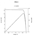
- the conversion efficiency of the compound photovoltaic cell 100 can be determined based on a I-V curve as illustrated in FIG. 4 .
- the conversion efficiency becomes higher if a current and a voltage become greater and the I-V curve has a square shape as illustrated in FIG. 4 .
- the I-V curve has a triangular shape, an adequate current is not obtained in accordance with an increase of the voltage. As a result, the conversion efficiency becomes lower.
- the tunnel junction layer 105 is formed of the p + -type GaInAs layer 105A and the n + -type InP layer 105B, it becomes possible to reduce the resistance of the tunnel joint interface of the tunnel junction layer 105. Since the compound photovoltaic cell 100 includes a plurality of the photoelectric conversion cells that constitute a multi-junction configuration having different band gaps with each other, it becomes possible to absorb the sunlight in a wide wavelength range. Accordingly, the conversion efficiency of the compound photovoltaic cell 100 is enhanced.
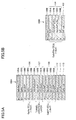
- FIGS. 5A, 5B , 6 , 7 and 8 are diagrams illustrating the production processes of the compound photovoltaic cell 120 according to the first embodiment.
- a layered body 100A is formed on a GaAs substrate 110, and a layered body 100B is formed on the InP substrate 103.
- a production method of the layered body 100A and 100B may be a Metal Organic Chemical Vapor Deposition (MOCVD) method, a Molecular Beam Epitaxy (MBE) method or the like.
- MOCVD Metal Organic Chemical Vapor Deposition
- MBE Molecular Beam Epitaxy
- a substrate other than the InP substrate 103 and the GaAs substrate 110 may be used.
- a combination of a GaSb substrate and a GaAs substrate, a combination of a Si substrate and a GaAs substrate or the like may be used instead of a combination of the InP substrate 103 and the GaAs substrate 110.
- the layered body 100A is formed by depositing an etch-stop-layer 111, a contact layer 112, the GaInP cell 108, the tunnel junction layer 107, the GaAs cell 106, the p + -type GaAs layer 105C and the p + -type GaInAs layer 105A onto the GaAs substrate 110 in this order (see FIG. 5A ).
- the GaAs cell 106 and the GaInP cell 108 are lattice matched with the GaAs substrate 110.
- a lattice constant of GaAs is about 5.65 ⁇ . It is preferable to adjust the composition ratio of each layer included in the III-V group compound semiconductor material so that lattice constants of the GaAs cell 106 and the GaInP cell 108 formed on the GaAs substrate 110 become close to 5.65 ⁇ .
- the layered body 100B is formed by depositing the GaInPAs cell 104 and the n + -type InP layer 105B onto the InP substrate 103 in this order (see FIG. 5B ).
- the GaInPAs cell 104 is lattice matched with the InP substrate 103.
- a lattice constant of InP is about 5.87 ⁇ . It is preferable to adjust the composition ratio of each layer included in the III-V group compound semiconductor material so that lattice constant of the GaInPAs cell 104 formed on the InP substrate 103 become close to 5.87 ⁇ .
- the lattice constant of the GaAs cell 106 and the GaInP cell 108 and the lattice constant of the GaInPAs cell 104 are different from each other, it is difficult to form the GaAs cell 106, the GaInP cell 108 and the GaInPAs cell 104 onto a single substrate. Accordingly, the layered body 100A and the layered body 100B are formed separately.
- the lattice constant of the p + -type GaInAs layer 105A or the p + -type AlGaInAs layer 105A1 is preferable to adjust the lattice constant of the p + -type GaInAs layer 105A or the p + -type AlGaInAs layer 105A1 so that the lattice constant becomes closer to a lattice constant of the GaAs substrate 110 rather than a lattice constant of the InP substrate 103.
- the layered body 100A which includes epitaxially-grown photoelectric conversion cells formed on the GaAs substrate 110 and the layered body 100B which includes an epitaxially grown photoelectric conversion cell formed on the InP substrate 103 are bonded directly as illustrated in FIG. 6 .
- a cleaning process and a surface activation treatment are performed to the surface of the p + -type GaInAs layer 105A and the surface of the n + -type InP layer 105B.
- the GaInAs layer 105A is a top layer of the layered body 100A and the n + -type InP layer 105B is a top layer of the layered body 100B.
- the surface of the p + -type GaInAs layer 105A and the surface of the n + -type InP layer 105B are bonded in a vacuum.
- a nitrogen plasma (N 2 plasma) treatment or the like is performed as the surface activation treatment. It is preferable to bond the surfaces at about 150 °C.
- the GaAs substrate 110 and the etch-stop-layer 111 are selectively etched and removed as illustrated in FIG. 7 .
- the GaAs substrate 110 is etched by a wet etching or the like.
- an etching solution is a mixed solution of sulfuric acid (H 2 SO 4 ), hydrogen peroxide (H 2 O 2 ) and water (H 2 O), for example. Since the mixed solution does not dissolve GaInP used as the etch-stop-layer 111, it is possible to stop the etching process in front of the etch-stop-layer 111. Accordingly, only the GaAs substrate 110 is etched accurately.
- the etch-stop-layer 111 is etched by a wet etching or the like.
- an etching solution is a mixed solution of hydrochloric acid (HCl) and water (H 2 O), for example.
- the GaAs substrate 110 and the etch-stop-layer 111 are selectively removed from the layered body 100A.
- a photo resist is applied on the contact layer 112, and then the photo resist is patterned by performing an exposure and a development that can be realized by a known photolithography process utilizing a photolithography machine. Accordingly, a patterned resist is formed on the contact layer 112.
- an electrode material is vapor-deposited on the contact layer 112 and the patterned resist by performing a vacuum deposition method or the like, in order to deposit a metallic film.
- the electrode 101 is formed on the contact layer 112 by lifting off the metallic film formed on the patterned resist.
- the contact layer 109 is formed by removing a part of the contact layer 112 which is not stacked with the electrode 101.
- the removing process is performed by wet etching utilizing the electrode 101 as a mask.
- an etching solution is a mixed solution of sulfuric acid (H 2 SO 4 ), hydrogen peroxide (H 2 O 2 ) and water (H 2 O), for example. Since the mixed solution does not dissolve the AlInP included in the GaInP cell 108, it is possible to stop the etching process in front of the n-type Al(x)InP layer 108A. Accordingly, only the contact layer 112 is etched accurately.
- the electrode 102 is formed under the InP substrate 103.
- the electrode 102 may be formed by performing a similar process to that of the electrode 101.
- the electrode 102 may be formed after polishing the InP substrate 103 to a designated thickness.
- the compound photovoltaic cell 120 is completed as illustrated in FIG. 8 .
- the production method of the compound photovoltaic cell 120 including the tunnel junction layer 105 having a three-layered configuration including the p + -type GaAs layer 105C, the p + -type GaInAs layer 105A and the n + -type InP layer 105B is described. If the number of layers included in the tunnel junction layer 105 is varied, a compound photovoltaic cell including the varied tunnel junction layer 105 can be formed by a production method similar to the production method as described above.
- the compound photovoltaic cell 100 can be formed by a production method similar to the production method as described above. Further, for example, in a case where the tunnel junction layer 105 has a two layered configuration including p + -type AlGaInAs layer 105A1 and the n + -type InP layer 105B, the compound photovoltaic cell 100 can be formed by a production method similar to the production method as described above.
- the compound photovoltaic cells 100 and 120 have the tunnel junction layers 105 in which the p + -type GaInAs layer 105A (or the p + -type AlGaInAs layer 105A1) and the n + -type InP layer 105B are joined at the joint interface of the layered body 100A and the layered body 100B. Accordingly, the resistance at the joint interface is reduced and it becomes easier for the tunnel current to flow through the tunnel junction layer 105. Therefore, it is possible to enhance the conversion efficiency of the compound photovoltaic cells 100 and 120.
- FIG. 9 is a diagram illustrating a compound photovoltaic cell 130 according to the second embodiment.
- the compound photovoltaic cell 130 includes four photoelectric conversion cells and three tunnel junction layers. Otherwise, the compound photovoltaic cell 130 includes the same configuration as that of the compound photovoltaic cell 120 as illustrated in FIG. 2 .
- a GaInAs cell 116 is formed on the InP substrate 103 and a tunnel junction layer 115 is formed between the GaInAs cell 116 and the GaInPAs cell 104.
- band gaps of the photoelectric conversion cells becomes smaller from an incident side to a back side along a light incident direction.
- the band gaps of the GaInP cell 108, the GaAs cell 106, the GaInPAs cell 104 and the GaInAs cell 116 are 1.9 eV, 1.42 eV, 1.0 eV and 0.75 eV, respectively.
- the tunnel junction layer 115 includes a p + -type Al(x)InAs layer 115A and a n + -type InP layer 115B.
- the p + -type Al(x)InAs layer 115A and the n + -type InP layer 115B are highly doped layers.
- the GaInAs cell 116 includes an n-type InP layer 116A, an n-type Ga(x)InAs layer 116B, a p-type Ga(x)InAs layer 116C and a p-type InP layer 116D that are formed in this order along the light incident direction.
- the n-type InP layer 116A is a window layer.
- the p-type InP layer 116D is a Back Surface Field (BSF) layer.
- BSF Back Surface Field
- Composition ratios of Ga (Gallium) of the n-type Ga(x)InAs layer 116B and the p-type Ga(x)InAs layer 116C are adjusted so that the band gap of the GaInAs cell 116 becomes 0.75 eV.
- An impurity of the n-type Ga(x)InAs layer 116B may be Si (Silicon), for example.
- An impurity of the p-type Ga(x)InAs layer 116C may be Zn (Zinc), for example.
- the compound photovoltaic cell 130 is a four-junction photovoltaic cell including the GaInP cell 108, the GaAs cell 106, the GaInPAs cell 104 and the GaInAs cell 116 of which the band gaps are 1.9 eV, 1.42 eV, 1.0 eV and 0.75 eV, respectively.
- the four-junction photovoltaic cell has well balanced band gaps as described above. Therefore, the compound photovoltaic cell 130 can further enhance energy conversion efficiency of the sunlight compared with the three-junction photovoltaic cell.
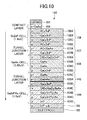
- FIG. 10 is a diagram illustrating a compound photovoltaic cell 140 according to the third embodiment.
- the compound photovoltaic cell 140 includes a tunnel junction layer 145 and a GaInPAs cell 144 instead of the tunnel junction layer 105 and the GaInPAs cell 104 as illustrated in FIG. 2 .
- the tunnel junction layer 145 includes the p + -type GaInAs layer 105A, the p + -type GaAs layer 105C and an n + -type Ga(x)InP layer 105D.
- the n + -type Ga(x)InP layer 105D have a tensile strain with respect to InP.
- the n + -type Ga(x)InP layer 105D is provided instead of the n + -type InP layer 105B and functions as an n + -type tunnel junction layer of the tunnel junction layer 145.
- the GaInPAs cell 144 includes a [Al(x)Ga](y)InAs layer 104E, the n-type Ga(x)InP(y)As layer 104B, the p-type Ga(x)InP(y)As layer 104C and the p-type InP layer 104D.
- the [Al(x)Ga](y)InAs layer 104E is provided instead of the n-type InP layer 104A and functions as a window layer of the GaInPAs cell 144.
- the compound photovoltaic cell 140 includes the same configuration as that of the compound photovoltaic cell 120 as illustrated in FIG. 2 .
- the n + -type Ga(x)InP layer 105D is highly doped.
- a composition ratio of Ga is 10%, a tensile strain is 0.7% and a band gap is 1.42 eV. It is necessary to adjust a thickness of the n + -type Ga(x)InP layer 105D so that the n + -type Ga(x)InP layer 105D does not have a lattice relaxation.
- the n + -type tunnel junction layer (n + -type Ga(x)InP layer 105D) be made of a material having a band gap greater than or equal to the band gap of the photoelectric conversion cell (for example, the GaAs cell 106) which is located next to the n + -type tunnel junction layer 105D on the back side in the light incident direction.
- the material may be GaPSb, GaInPSb, AlInAs, AlGaInAs, AIAsSb, AIGaAsSb, AlPSb, AIGaPSb, AlInPSb or the like other than GaInP, for example.
- the window layer (n-type InP layer 104A) is made of a material having a band gap greater than or equal to the band gap of the photoelectric conversion cell (for example, the GaAs cell 106) which is located next to the window layer on the incident side in the light incident direction.
- the band gap of the [Al(x)Ga](y)InAs layer 104E is more than or equal to 1.42 eV, preferably more than or equal to 1.5 eV.
- the material of the window layer may be GaInP, GaPSb, GaInPSb, AlInAs, AlGaInAs, AlAsSb, AIGaAsSb, AlPSb, AlGaPSb, AlPSb, AlInPSb or the like other than AlGaInAs for example.
- an InP (1.35 eV) layer has been widely used for an n + -type tunnel junction layer (wafer joint layer) or a window layer. Since the InP (1.35 eV) layer absorbs a part of the light transmitting through a GaAs cell (1.42 eV), conversion efficiency of the conventional compound photovoltaic cell is decreased.
- FIG. 11 is a diagram illustrating a compound photovoltaic cell 150 according to a fourth embodiment
- the compound photovoltaic cell 150 includes four photoelectric conversion cells and three tunnel junction layers.
- a compound photovoltaic cell 150 includes a tunnel junction layer 145 and a GaInPAs cell 144 instead of the tunnel junction layer 105 and the GaInPAs cell 104 as illustrated in FIG. 2 .
- the tunnel junction layer 145 includes the p + -type GaInAs layer 105A, the p + -type GaAs layer 105C and an n + -type Ga(x)InP layer 105D.
- the n + -type Ga(x)InP layer 105D has a tensile strain with respect to InP.
- the n + -type Ga(x)InP layer 105D is provided instead of the n + -type InP layer 105B and functions as an n + -type tunnel junction layer of the tunnel junction layer 145.
- the GaInPAs cell 144 includes a [Al(x)Ga](y)InAs layer 104E, the n-type Ga(x)InP(y)As layer 104B, the p-type Ga(x)InP(y)As layer 104C and the p-type InP layer 104D.
- the [Al(x)Ga](y)InAs layer 104E is provided instead of the n-type InP layer 104A and functions as a window layer of the GaInPAs cell 144.
- the compound photovoltaic cell 150 includes the same configuration as that of the compound photovoltaic cell 130 as illustrated in FIG. 9 .
- a GaInAs cell 116 is formed on the InP substrate 103 and a tunnel junction layer 115 is formed between the GaInAs cell 116 and the GaInPAs cell 144.
- the tunnel junction layer 145 includes the p + -type GaAs layer 105C, the p + -type GaInAs layer 105A and the n + -type Ga(x)InP layer 105D.
- the p + -type GaAs layer 105C, the p + -type GaInAs layer 105A and the n + -type Ga(x)InP layer 105D are highly doped layers.
- a composition ratio of Ga is 10% and a tensile strain with respect to InP is 0.7%.
- the compound photovoltaic cell 150 is a four-junction photovoltaic cell including the GaInP cell 108, the GaAs cell 106, the GaInPAs cell 144 and the GaInAs cell 116 of which the band gaps are 1.9 eV, 1.42 eV, 1.0 eV and 0.75 eV, respectively.
- a p + -type AlGaAs layer including A1 (Aluminum) may be included in the tunnel junction layer 145 instead of the p + GaAs layer 105C as illustrated in FIG. 11 .
- the p + -type AlGaInAs layer may be included instead of the p + -type GaInAs layer 105A. It is necessary to design the multi-junction photovoltaic cell so that currents generated in the cells have the same current values.
- the compound photovoltaic cell 150 is designed so that the GaAs cell 106 does not absorb all the light in a wavelength range which can be absorbed at the GaAs cell 106 but transmits a part of the light to the GaInPAs cell 144 and the GaInAs cell 116 located on the back side in the incident light direction with respect to the GaAs cell 106.
- the fourth embodiment it is possible to reduce an absorption of the light at the tunnel junction layer 145 by using the n + tunnel junction layer (wafer joint layer) made of GaInP or Ga(In)PSb having a wide band gap and the p + layer made of AlGaAs having a wide band gap. Accordingly, it becomes possible to cause the light transmitting through the tunnel junction layer 145 to enter the cell(s) formed on the InP substrate 103 efficiently. As a result, the conversion efficiency is enhanced.
- Ga(In)PSb includes GaPSb and GaInPSb.
- FIG. 12 is a diagram illustrating a compound photovoltaic cell 160 according to a fifth embodiment
- the compound photovoltaic cell 160 includes a tunnel junction layer 145 and a GaInPAs cell 144 instead of the tunnel junction layer 105 and the GaInPAs cell 104 as illustrated in FIG. 2 .
- the tunnel junction layer 145 includes the p + -type GaInAs layer 105A, the p + -type GaAs layer 105C and an n + -type Ga(x)InP layer 105D.
- the n + -type Ga(x)InP layer 105D has a tensile strain with respect to InP.
- the n + -type Ga(x)InP layer 105D is provided instead of the n + -type InP layer 105B and functions as an n + -type tunnel junction layer of the tunnel junction layer 145.
- the GaInPAs cell 144 includes a [Al(x)Ga](y)InAs layer 104E, the n-type Ga(x)InP(y)As layer 104B, the p-type Ga(x)InP(y)As layer 104C and the p-type InP layer 104D.
- the [Al(x)Ga](y)InAs layer 104E is provided instead of the n-type InP layer 104A and functions as a window layer of the GaInPAs cell 144.
- the compound photovoltaic cell 160 includes a GaInAs cell 166 instead of the GaAs cell 106.
- the GaInAs cell 166 includes an n-type [Al(x)Ga](y)InP layer 106A, an n-type Ga(x)InAs layer 106E, a p-type Ga(x)InAs layer 106F and a p-type Ga(x)InP layer 106D.
- the n-type Ga(x)InAs layer 106E and the p-type Ga(x)InAs layer 106F have compression strains.
- the compound photovoltaic cell 160 has the same configuration as that of the compound photovoltaic cell 140 as illustrated in FIG. 10 .
- the n + -type Ga(x)InP layer 105D is highly doped.
- a composition ratio of Ga is 7.0%, a tensile strain is 0.5% and a band gap is 1.40 eV.
- composition ratios of In (Indium) are 1.5%, tensile strains with respect to InP are 0.1% and band gaps are 1.40 eV.
- the n-type Ga(x)InAs layer 106E and the p-type Ga(x)InAs layer 106F have the same composition ratio of In, tensile strain and band gap with each other.
- the Ga(x)InAs layers 106E and 106F can have thicknesses that enable the Ga(x)InAs layers 106E and 106F to absorb adequate light and perform as a photoelectric conversion cell.
- an InP (1.35 eV) layer has been widely used for an n + -type tunnel junction layer (wafer joint layer) or a window layer. Since the InP (1.35 eV) layer absorbs a part of the light transmitting through a GaAs cell (1.42 eV), conversion efficiency of the conventional compound photovoltaic cell is decreased.
- the fifth embodiment it is possible to use the n + -type tunnel junction layer (wafer joint layer) and the window layer having narrower band gaps than the band gaps of the n + -type tunnel junction layer (wafer joint layer) and the window layer according to the third and fourth embodiments by including the GaInAs cell 166 (1.40 eV) instead of the GaAs cell 106 (1.42 eV).
- Small strain is enough for realizing the GaInP layer having the tensile strain. Accordingly, it is easy to form the GaInP layer having the tensile strain.
- FIG. 13 is a diagram illustrating a compound photovoltaic cell 170 according to a sixth embodiment.
- the compound photovoltaic cell 170 includes four photoelectric conversion cells and three tunnel junction layers. As illustrated in FIG. 13 , the compound photovoltaic cell 170 includes a tunnel junction layer 145 and a GaInPAs cell 144 instead of the tunnel junction layer 105 and the GaInPAs cell 104 as illustrated in FIG. 2 .
- the tunnel junction layer 145 includes the p + -type GaInAs layer 105A, the p + -type GaAs layer 105C and an n + -type Ga(x)InP layer 105D.
- the n + -type Ga(x)InP layer 105D has a tensile strain with respect to InP.
- the n + -type Ga(x)InP layer 105D is provided instead of the n + -type InP layer 105B and functions as an n + -type tunnel junction layer of the tunnel junction layer 145.
- the GaInPAs cell 144 includes a [Al(x)Ga](y)InAs layer 104E, the n-type Ga(x)InP(y)As layer 104B, the p-type Ga(x)InP(y)As layer 104C and the p-type InP layer 104D.
- the [Al(x)Ga](y)InAs layer 104E is provided instead of the n-type InP layer 104A and functions as a window layer of the GaInPAs cell 144.
- the compound photovoltaic cell 170 includes a GaInAs cell 166 instead of the GaAs cell 106.
- the GaInAs cell 166 includes an n-type [Al(x)Ga](y)InP layer 106A, an n-type Ga(x)InAs layer 106E, a p-type Ga(x)InAs layer 106F and a p-type Ga(x)InP layer 106D.
- the n-type Ga(x)InAs layer 106E and the p-type Ga(x)InAs layer 106F have compression strains.
- the compound photovoltaic cell 170 has the same configuration as that of the compound photovoltaic cell 150 as illustrated in FIG. 11 .
- the n + -type Ga(x)InP layer 105D is highly doped.
- a composition ratio of Ga is 7.0%, a tensile strain is 0.5% and a band gap is 1.40 eV.
- composition ratios of In (Indium) are 1.5%, tensile strains with respect to InP are 0.1% and band gaps are 1.40 eV.
- the n-type Ga(x)InAs layer 106E and the p-type Ga(x)InAs layer 106F have the same composition ratio of In, tensile strain and band gap with each other.
- the compound photovoltaic cell 170 is a four-junction photovoltaic cell including the GaInP cell 108, the GaInAs cell 166, the GaInPAs cell 144 and the GaInAs cell 116 of which the band gaps are 1.9 eV, 1.40 eV, 1.0 eV and 0.75 eV, respectively.
- the compound photovoltaic cell is not limited to the specific embodiments described herein, and variations and modifications may be made without departing from the scope of the present invention.
Landscapes
- Life Sciences & Earth Sciences (AREA)
- Engineering & Computer Science (AREA)
- Sustainable Energy (AREA)
- Photovoltaic Devices (AREA)
- Sustainable Development (AREA)
Applications Claiming Priority (2)
| Application Number | Priority Date | Filing Date | Title |
|---|---|---|---|
| JP2013157477 | 2013-07-30 | ||
| JP2014118296A JP6550691B2 (ja) | 2013-07-30 | 2014-06-09 | 化合物半導体太陽電池 |
Publications (2)
| Publication Number | Publication Date |
|---|---|
| EP2833413A2 true EP2833413A2 (de) | 2015-02-04 |
| EP2833413A3 EP2833413A3 (de) | 2015-02-25 |
Family
ID=51224829
Family Applications (1)
| Application Number | Title | Priority Date | Filing Date |
|---|---|---|---|
| EP14178623.6A Withdrawn EP2833413A3 (de) | 2013-07-30 | 2014-07-25 | Photovoltaische Zelle aus Verbindungshalbleiter |
Country Status (4)
| Country | Link |
|---|---|
| US (2) | US20150034153A1 (de) |
| EP (1) | EP2833413A3 (de) |
| JP (1) | JP6550691B2 (de) |
| CN (1) | CN104393086B (de) |
Families Citing this family (10)
| Publication number | Priority date | Publication date | Assignee | Title |
|---|---|---|---|---|
| JP6248623B2 (ja) | 2013-02-18 | 2017-12-20 | 株式会社リコー | 反応材及びケミカルヒートポンプ |
| JP6582591B2 (ja) | 2014-07-11 | 2019-10-02 | 株式会社リコー | 化合物半導体太陽電池、及び、化合物半導体太陽電池の製造方法 |
| JP6536220B2 (ja) * | 2015-06-29 | 2019-07-03 | 株式会社リコー | 化合物半導体太陽電池及びその製造方法 |
| US20170084771A1 (en) * | 2015-09-21 | 2017-03-23 | The Boeing Company | Antimonide-based high bandgap tunnel junction for semiconductor devices |
| CN106449848B (zh) * | 2016-10-28 | 2017-09-29 | 上海空间电源研究所 | 一种含有复合多光子腔的多结太阳电池 |
| CN108735848B (zh) * | 2017-04-17 | 2020-09-01 | 中国科学院苏州纳米技术与纳米仿生研究所 | 多结叠层激光光伏电池及其制作方法 |
| DE102017005950A1 (de) * | 2017-06-21 | 2018-12-27 | Azur Space Solar Power Gmbh | Solarzellenstapel |
| CN107482069A (zh) * | 2017-07-10 | 2017-12-15 | 宋亮 | 一种多结化合物太阳能电池及其生产工艺 |
| DE102020001185A1 (de) | 2020-02-25 | 2021-08-26 | Azur Space Solar Power Gmbh | Stapelförmige monolithische aufrecht-metamorphe lll-V-Mehrfachsolarzelle |
| CN113690335B (zh) * | 2021-10-26 | 2022-03-08 | 南昌凯迅光电股份有限公司 | 一种改善型三结砷化镓太阳电池及其制作方法 |
Citations (3)
| Publication number | Priority date | Publication date | Assignee | Title |
|---|---|---|---|---|
| US5679963A (en) * | 1995-12-05 | 1997-10-21 | Sandia Corporation | Semiconductor tunnel junction with enhancement layer |
| US20120138116A1 (en) | 2010-12-03 | 2012-06-07 | The Boeing Company | Direct wafer bonding |
| WO2014142340A1 (en) * | 2013-03-14 | 2014-09-18 | Ricoh Company, Ltd. | Compound semiconductor photovoltaic cell and manufacturing method of the same |
Family Cites Families (22)
| Publication number | Priority date | Publication date | Assignee | Title |
|---|---|---|---|---|
| US5183779A (en) * | 1991-05-03 | 1993-02-02 | The United States Of America As Represented By The Secretary Of The Navy | Method for doping GaAs with high vapor pressure elements |
| US5769964A (en) * | 1996-08-29 | 1998-06-23 | The United States Of America As Reprresented By The United States Department Of Energy | Bulk single crystal ternary substrates for a thermophotovoltaic energy conversion system |
| US8173891B2 (en) * | 2002-05-21 | 2012-05-08 | Alliance For Sustainable Energy, Llc | Monolithic, multi-bandgap, tandem, ultra-thin, strain-counterbalanced, photovoltaic energy converters with optimal subcell bandgaps |
| US7071407B2 (en) * | 2002-10-31 | 2006-07-04 | Emcore Corporation | Method and apparatus of multiplejunction solar cell structure with high band gap heterojunction middle cell |
| US7294868B2 (en) * | 2004-06-25 | 2007-11-13 | Finisar Corporation | Super lattice tunnel junctions |
| US11211510B2 (en) * | 2005-12-13 | 2021-12-28 | The Boeing Company | Multijunction solar cell with bonded transparent conductive interlayer |
| US20130139877A1 (en) * | 2007-09-24 | 2013-06-06 | Emcore Solar Power, Inc. | Inverted metamorphic multijunction solar cell with gradation in doping in the window layer |
| JP5283588B2 (ja) * | 2008-12-26 | 2013-09-04 | 京セラ株式会社 | 太陽電池 |
| US8299351B2 (en) * | 2009-02-24 | 2012-10-30 | Hong Kong Applied Science And Technology Research Institute Co., Ltd. | Epitaxial growth of III-V compounds on (111) silicon for solar cells |
| WO2010113361A1 (ja) * | 2009-04-03 | 2010-10-07 | シャープ株式会社 | 照明装置、表示装置、及びテレビ受信装置 |
| EP2251912A1 (de) * | 2009-05-11 | 2010-11-17 | Fraunhofer-Gesellschaft zur Förderung der angewandten Forschung e.V. | Tunneldioden aus spannungskompensierten Verbindungshalbleiterschichten |
| JP5481665B2 (ja) * | 2009-09-30 | 2014-04-23 | 旭化成エレクトロニクス株式会社 | 多接合型太陽電池 |
| CN101950774A (zh) * | 2010-08-17 | 2011-01-19 | 中国科学院苏州纳米技术与纳米仿生研究所 | 四结GaInP/GaAs/InGaAsP/InGaAs太阳电池的制作方法 |
| US11417788B2 (en) | 2010-11-19 | 2022-08-16 | The Boeing Company | Type-II high bandgap tunnel junctions of InP lattice constant for multijunction solar cells |
| KR101344910B1 (ko) * | 2011-07-04 | 2013-12-26 | 네이버 주식회사 | 클라우드를 기반으로 서비스 간의 문서를 연결하는 시스템 및 방법 |
| US20130048063A1 (en) | 2011-08-26 | 2013-02-28 | The Government Of The United States Of America, As Represented By The Secretary Of The Navy | Multijunction Solar Cells Lattice Matched to InP Using Sb-Containing Alloys |
| US8884157B2 (en) | 2012-05-11 | 2014-11-11 | Epistar Corporation | Method for manufacturing optoelectronic devices |
| US20140001509A1 (en) | 2012-06-27 | 2014-01-02 | Epistar Corporation | Optoelectronic semiconductor device and the manufacturing method thereof |
| US11646388B2 (en) | 2012-09-14 | 2023-05-09 | The Boeing Company | Group-IV solar cell structure using group-IV or III-V heterostructures |
| JP2014123712A (ja) | 2012-11-26 | 2014-07-03 | Ricoh Co Ltd | 太陽電池の製造方法 |
| US9252297B2 (en) | 2012-12-04 | 2016-02-02 | Epistar Corporation | Optoelectronic device and the manufacturing method thereof |
| CN103219414B (zh) * | 2013-04-27 | 2016-12-28 | 中国科学院苏州纳米技术与纳米仿生研究所 | GaInP/GaAs/InGaAsP/InGaAs四结级联太阳电池的制作方法 |
-
2014
- 2014-06-09 JP JP2014118296A patent/JP6550691B2/ja active Active
- 2014-07-25 EP EP14178623.6A patent/EP2833413A3/de not_active Withdrawn
- 2014-07-29 US US14/445,249 patent/US20150034153A1/en not_active Abandoned
- 2014-07-30 CN CN201410541385.2A patent/CN104393086B/zh active Active
-
2017
- 2017-04-10 US US15/483,633 patent/US10490684B2/en active Active
Patent Citations (3)
| Publication number | Priority date | Publication date | Assignee | Title |
|---|---|---|---|---|
| US5679963A (en) * | 1995-12-05 | 1997-10-21 | Sandia Corporation | Semiconductor tunnel junction with enhancement layer |
| US20120138116A1 (en) | 2010-12-03 | 2012-06-07 | The Boeing Company | Direct wafer bonding |
| WO2014142340A1 (en) * | 2013-03-14 | 2014-09-18 | Ricoh Company, Ltd. | Compound semiconductor photovoltaic cell and manufacturing method of the same |
Non-Patent Citations (3)
| Title |
|---|
| NAKAYAMA KEISUKE ET AL: "Improved electrical properties of wafer-bonded p-GaAs/n-InP interfaces with sulfide passivation", JOURNAL OF APPLIED PHYSICS, vol. 103, 2 May 2008 (2008-05-02), pages 94503-1 - 94503-5, XP012110820, ISSN: 0021-8979, DOI: 10.1063/1.2912717 * |
| PROCEEDINGS OF THE 29TH IEEE PHOTOVOLTAIC SPECIALISTS CONFERENCE, 2010, pages 412 - 417 |
| ZOLPER J C ET AL: "GaAsSb-BASED HETEROJUNCTION TUNNEL DIODES FOR TANDEM SOLAR CELL INTERCONNECTS", PROC. OF THE WORLD CONFERENCE ON PHOTOVOLTAIC ENERGY, vol. 1, 5 December 1994 (1994-12-05) - 9 December 1994 (1994-12-09), pages 1843 - 1846, XP000680158, ISBN: 978-0-7803-1460-3, DOI: 10.1109/WCPEC.1994.520724 * |
Also Published As
| Publication number | Publication date |
|---|---|
| CN104393086A (zh) | 2015-03-04 |
| CN104393086B (zh) | 2017-06-20 |
| EP2833413A3 (de) | 2015-02-25 |
| US20150034153A1 (en) | 2015-02-05 |
| JP2015046572A (ja) | 2015-03-12 |
| JP6550691B2 (ja) | 2019-07-31 |
| US20170213932A1 (en) | 2017-07-27 |
| US10490684B2 (en) | 2019-11-26 |
Similar Documents
| Publication | Publication Date | Title |
|---|---|---|
| US10490684B2 (en) | Method for producing a compound photovoltaic cell | |
| US10008627B2 (en) | Photovoltaic cell and photovoltaic cell manufacturing method | |
| US8450773B1 (en) | Strain-compensated infrared photodetector and photodetector array | |
| CN106663714B (zh) | 化合物-半导体光伏电池及化合物-半导体光伏电池的制造方法 | |
| TWI583012B (zh) | 化合物半導體太陽能電池及其製造方法 | |
| JP6446782B2 (ja) | 化合物半導体太陽電池、及び、化合物半導体太陽電池の製造方法 | |
| CN103189998A (zh) | 用于多结太阳能电池的InP晶格常数的II型高带隙隧道结 | |
| EP3010046B1 (de) | Photovoltaische verbindungshalbleiterzelle und herstellungsverfahren einer photovoltaischen verbindungshalbleiterzelle | |
| US20160013336A1 (en) | Compound-semiconductor photovoltaic cell and manufacturing method of compound-semiconductor photovoltaic cell | |
| JP2015038952A (ja) | 化合物半導体太陽電池、及び、化合物半導体太陽電池の製造方法 | |
| Vadiee et al. | AlGaSb based solar cells grown on GaAs by Molecular Beam Epitaxy | |
| JP6164685B2 (ja) | 太陽電池 | |
| Sodabanlu et al. | Lattice-matched 3-junction cell with 1.2-eV InGaAs/GaAsP superlattice middle cell for improved current matching |
Legal Events
| Date | Code | Title | Description |
|---|---|---|---|
| PUAL | Search report despatched |
Free format text: ORIGINAL CODE: 0009013 |
|
| 17P | Request for examination filed |
Effective date: 20140725 |
|
| AK | Designated contracting states |
Kind code of ref document: A2 Designated state(s): AL AT BE BG CH CY CZ DE DK EE ES FI FR GB GR HR HU IE IS IT LI LT LU LV MC MK MT NL NO PL PT RO RS SE SI SK SM TR |
|
| AX | Request for extension of the european patent |
Extension state: BA ME |
|
| PUAI | Public reference made under article 153(3) epc to a published international application that has entered the european phase |
Free format text: ORIGINAL CODE: 0009012 |
|
| AK | Designated contracting states |
Kind code of ref document: A3 Designated state(s): AL AT BE BG CH CY CZ DE DK EE ES FI FR GB GR HR HU IE IS IT LI LT LU LV MC MK MT NL NO PL PT RO RS SE SI SK SM TR |
|
| AX | Request for extension of the european patent |
Extension state: BA ME |
|
| RIC1 | Information provided on ipc code assigned before grant |
Ipc: H01L 31/0687 20120101AFI20150122BHEP Ipc: H01L 31/18 20060101ALI20150122BHEP Ipc: H01L 31/0304 20060101ALI20150122BHEP |
|
| STAA | Information on the status of an ep patent application or granted ep patent |
Free format text: STATUS: EXAMINATION IS IN PROGRESS |
|
| 17Q | First examination report despatched |
Effective date: 20170529 |
|
| GRAP | Despatch of communication of intention to grant a patent |
Free format text: ORIGINAL CODE: EPIDOSNIGR1 |
|
| STAA | Information on the status of an ep patent application or granted ep patent |
Free format text: STATUS: GRANT OF PATENT IS INTENDED |
|
| RIC1 | Information provided on ipc code assigned before grant |
Ipc: H01L 31/18 20060101ALI20210202BHEP Ipc: H01L 31/0693 20120101ALI20210202BHEP Ipc: H01L 31/0304 20060101ALI20210202BHEP Ipc: H01L 31/0687 20120101AFI20210202BHEP |
|
| INTG | Intention to grant announced |
Effective date: 20210305 |
|
| STAA | Information on the status of an ep patent application or granted ep patent |
Free format text: STATUS: THE APPLICATION IS DEEMED TO BE WITHDRAWN |
|
| 18D | Application deemed to be withdrawn |
Effective date: 20210716 |