EP2833235B1 - Flexible touch panel with bendable active area - Google Patents
Flexible touch panel with bendable active area Download PDFInfo
- Publication number
- EP2833235B1 EP2833235B1 EP14172733.9A EP14172733A EP2833235B1 EP 2833235 B1 EP2833235 B1 EP 2833235B1 EP 14172733 A EP14172733 A EP 14172733A EP 2833235 B1 EP2833235 B1 EP 2833235B1
- Authority
- EP
- European Patent Office
- Prior art keywords
- active area
- touch
- sensing electrodes
- area
- touch window
- Prior art date
- Legal status (The legal status is an assumption and is not a legal conclusion. Google has not performed a legal analysis and makes no representation as to the accuracy of the status listed.)
- Active
Links
Images


Classifications
-
- G—PHYSICS
- G06—COMPUTING OR CALCULATING; COUNTING
- G06F—ELECTRIC DIGITAL DATA PROCESSING
- G06F3/00—Input arrangements for transferring data to be processed into a form capable of being handled by the computer; Output arrangements for transferring data from processing unit to output unit, e.g. interface arrangements
- G06F3/01—Input arrangements or combined input and output arrangements for interaction between user and computer
- G06F3/03—Arrangements for converting the position or the displacement of a member into a coded form
- G06F3/041—Digitisers, e.g. for touch screens or touch pads, characterised by the transducing means
- G06F3/0412—Digitisers structurally integrated in a display
-
- G—PHYSICS
- G06—COMPUTING OR CALCULATING; COUNTING
- G06F—ELECTRIC DIGITAL DATA PROCESSING
- G06F1/00—Details not covered by groups G06F3/00 - G06F13/00 and G06F21/00
- G06F1/16—Constructional details or arrangements
- G06F1/1613—Constructional details or arrangements for portable computers
- G06F1/1633—Constructional details or arrangements of portable computers not specific to the type of enclosures covered by groups G06F1/1615 - G06F1/1626
- G06F1/1637—Details related to the display arrangement, including those related to the mounting of the display in the housing
- G06F1/1641—Details related to the display arrangement, including those related to the mounting of the display in the housing the display being formed by a plurality of foldable display components
-
- G—PHYSICS
- G06—COMPUTING OR CALCULATING; COUNTING
- G06F—ELECTRIC DIGITAL DATA PROCESSING
- G06F1/00—Details not covered by groups G06F3/00 - G06F13/00 and G06F21/00
- G06F1/16—Constructional details or arrangements
- G06F1/1613—Constructional details or arrangements for portable computers
- G06F1/1633—Constructional details or arrangements of portable computers not specific to the type of enclosures covered by groups G06F1/1615 - G06F1/1626
- G06F1/1637—Details related to the display arrangement, including those related to the mounting of the display in the housing
- G06F1/1652—Details related to the display arrangement, including those related to the mounting of the display in the housing the display being flexible, e.g. mimicking a sheet of paper, or rollable
-
- G—PHYSICS
- G06—COMPUTING OR CALCULATING; COUNTING
- G06F—ELECTRIC DIGITAL DATA PROCESSING
- G06F3/00—Input arrangements for transferring data to be processed into a form capable of being handled by the computer; Output arrangements for transferring data from processing unit to output unit, e.g. interface arrangements
- G06F3/01—Input arrangements or combined input and output arrangements for interaction between user and computer
- G06F3/03—Arrangements for converting the position or the displacement of a member into a coded form
- G06F3/041—Digitisers, e.g. for touch screens or touch pads, characterised by the transducing means
- G06F3/044—Digitisers, e.g. for touch screens or touch pads, characterised by the transducing means by capacitive means
- G06F3/0445—Digitisers, e.g. for touch screens or touch pads, characterised by the transducing means by capacitive means using two or more layers of sensing electrodes, e.g. using two layers of electrodes separated by a dielectric layer
-
- G—PHYSICS
- G06—COMPUTING OR CALCULATING; COUNTING
- G06F—ELECTRIC DIGITAL DATA PROCESSING
- G06F3/00—Input arrangements for transferring data to be processed into a form capable of being handled by the computer; Output arrangements for transferring data from processing unit to output unit, e.g. interface arrangements
- G06F3/01—Input arrangements or combined input and output arrangements for interaction between user and computer
- G06F3/03—Arrangements for converting the position or the displacement of a member into a coded form
- G06F3/041—Digitisers, e.g. for touch screens or touch pads, characterised by the transducing means
- G06F3/044—Digitisers, e.g. for touch screens or touch pads, characterised by the transducing means by capacitive means
- G06F3/0448—Details of the electrode shape, e.g. for enhancing the detection of touches, for generating specific electric field shapes, for enhancing display quality
-
- G—PHYSICS
- G06—COMPUTING OR CALCULATING; COUNTING
- G06F—ELECTRIC DIGITAL DATA PROCESSING
- G06F3/00—Input arrangements for transferring data to be processed into a form capable of being handled by the computer; Output arrangements for transferring data from processing unit to output unit, e.g. interface arrangements
- G06F3/01—Input arrangements or combined input and output arrangements for interaction between user and computer
- G06F3/03—Arrangements for converting the position or the displacement of a member into a coded form
- G06F3/041—Digitisers, e.g. for touch screens or touch pads, characterised by the transducing means
- G06F3/047—Digitisers, e.g. for touch screens or touch pads, characterised by the transducing means using sets of wires, e.g. crossed wires
-
- H—ELECTRICITY
- H01—ELECTRIC ELEMENTS
- H01B—CABLES; CONDUCTORS; INSULATORS; SELECTION OF MATERIALS FOR THEIR CONDUCTIVE, INSULATING OR DIELECTRIC PROPERTIES
- H01B5/00—Non-insulated conductors or conductive bodies characterised by their form
- H01B5/14—Non-insulated conductors or conductive bodies characterised by their form comprising conductive layers or films on insulating-supports
-
- G—PHYSICS
- G06—COMPUTING OR CALCULATING; COUNTING
- G06F—ELECTRIC DIGITAL DATA PROCESSING
- G06F2203/00—Indexing scheme relating to G06F3/00 - G06F3/048
- G06F2203/041—Indexing scheme relating to G06F3/041 - G06F3/045
- G06F2203/04102—Flexible digitiser, i.e. constructional details for allowing the whole digitising part of a device to be flexed or rolled like a sheet of paper
Definitions
- the disclosure relates to a touch window and a touch device including the same.
- a touch panel which performs an input function through the touch of an image displayed on a touch device by an input device, such as a stylus pen or a hand, has been applied to various electronic appliances.
- the touch panel may be typically classified into a resistive touch panel and a capacitive touch panel.
- the position of the touch point is detected by detecting the variation of resistance according to the connection between electrodes when pressure is applied to an input device.
- the position of the touch point is detected by detecting the variation in capacitance when a finger of the user is touched on the capacitive touch panel between electrodes.
- ITO indium tin oxide
- the transparent electrode of the touch panel is easy to be physically damaged when the substrate is flexed and bent, so that the electrode property is deteriorated. Therefore, the indium tin oxide (ITO) is not suitable for a flexible device.
- ITO indium tin oxide
- Document US 2012/113614 A1 discloses a touch window comprising a substrate in which an active area and an unactive area are defined.
- the active area comprising a first flat active area and a second curved active area bent from the first area to form a curved touch window.
- the active area i.e. the first flat and second curved active areas, include transparent first and second sensing electrodes formed of, for example ITO and extending in crossed first and second directions.
- the active area being driven in capacitance touch difference scheme between the first and second sensing electrodes.
- Document US 2012/313887 A1 discloses a touch window including a substrate in which an active area and an unactive area are defined.
- the active area includes transparent, e.g. ITO, first electrodes extending in a first direction and second flexible, e.g. nano-tubes, sensing electrodes extending in a second direction crossing the first direction.
- the active area being driven in capacitance touch difference scheme between the first and second sensing electrodes.
- Touch window comprising first and second sensing driven in capacitance touch difference scheme between the sensing electrodes, which may include at least one of indium tin oxide (ITO), indium zinc oxide (IZO), zinc oxide, a carbon nano-tube (CNT), an Ag Nano wire, a conductive polymer, and a grapheme on the transparent substrate.
- ITO indium tin oxide
- IZO indium zinc oxide
- CNT carbon nano-tube
- Ag Nano wire Ag Nano wire
- a conductive polymer a grapheme on the transparent substrate.
- Document US 2012/127112 A1 discloses a flexible touch window comprising first and second transparent electrodes driven in capacitance touch difference scheme between the sensing electrodes, wherein materials of the first transparent electrodes and the second transparent patterned electrodes respectively comprise transparent conductive oxide, an organic transparent conductive material, nano metal or carbon nanotube.
- a touch window including a substrate in which an active area and an unactive area are defined; and a sensing electrode on the active area to sense a position, wherein the active area includes a first active area; and a second active area adjacent to the first active area and driven in a driving scheme different from a driving scheme for the first active area.
- the touch window according to the invention includes the first and second active areas. Since the first and second active areas are driven in mutually different schemes, various types of touch windows can be provided. That is, the first active area is driven in the same manner as that of the related art and the positions in upper and lower directions are recognized in the second active area, so that the touch window can be driven in a manner such as sound volume, enlarging or reducing of a screen, or moving up or down. Thus, user experience can expand.
- the first active area includes the first and second sensing electrodes, the first sensing electrode including a material useful for the visibility, so that the visibility in the first active area can be maintained.
- the second active area can be bent from the first active area. That is, the second active area is bendable.
- a third sensing electrode is provided in the second active area.
- the third sensing electrode includes a material having a flexible property, so that the third sensing electrode can be bent without any physical damage.
- the second active area which is bendable can be formed simultaneously with the first active area, so that the process can be simplified.
- each layer shown in the drawings may be exaggerated, omitted or schematically drawn for the purpose of convenience or clarity.
- the size of elements does not utterly reflect an actual size.
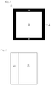
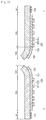
- FIG. 1 is a schematic plan view showing a touch window according to an embodiment.
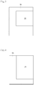
- FIGS. 2 to 4 are schematic plan views showing a touch window according to another embodiment.
- a touch window 10 includes a substrate 100 having an active area AA, in which a position of an input device (e.g., finger) is detected, and an unactive area UA provided at a peripheral portion of the active area AA.
- an input device e.g., finger
- sensing electrodes 200 may be formed in the active area AA such that the input device may be sensed.
- Wires 300 electrically connecting the sensing electrodes 200 to each other are formed in the unactive area UA.
- an external circuit connected to the wires 300 may be placed in the unactive area UA.
- the unactive area UA may surround the active area AA.
- the active area AA may include four sides and the unactive area AA may be provided at all of the four sides. That is, the unactive area UA may surround a rim of the active area AA.
- the unactive area UA may be provided at only one side of the active area AA.
- the unactive area UA may be provided at one among four sides of the active area.
- the unactive area UA may provided at three among the four sides of the active area AA. That is, the unactive area UA may be provided at all sides of the active AA except for one side of the active area AA.
- the unactive area UA may be provided at two among the four sides of the active area AA.
- the flexible area of the touch window may be variously formed by variously disposing the unactive area UA.
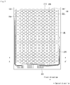
- FIG. 5 is a plan view showing a touch window according to an embodiment.
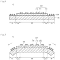
- FIGS. 6 and 7 are sectional views taken along line A-A' of FIG. 5 .
- the substrate 100 may be formed of various materials to support a sensing electrode 200, a wire 300 and a circuit substrate formed on the substrate.
- the substrate 100 may include a glass substrate or a plastic substrate including polyethylene terephthalate (PET) film or resin.
- PET polyethylene terephthalate
- the outer dummy layer is formed in the unactive area UA of the substrate 100.
- the outer dummy layer may be coated with a material having a predetermined color so that the wires 300 and a printed circuit board connecting the wires 300 to external circuits cannot be viewed from the outside.
- the outer dummy layer may have a color suitable for a desired outer appearance thereof.
- the outer dummy layer includes black pigments to represent black.
- a desired logo may be formed in the outer dummy layer through various schemes.
- the outer dummy layer may be formed through deposition, print, and wet coating schemes.
- the active area AA of the substrate 100 includes first and second areas 1AA and 2AA.
- Sensing electrodes 200, 210, 220, 230 are provided on the active area AA. Two types of sensing electrodes 210 and 220 are provided in the first active area 1AA. The sensing electrodes 200, 210, 220, 230 sense whether an input device such as a finger makes contact with the sensing electrodes 200, 210, 220, 230.
- the sensing electrode 200 includes first and second sensing electrodes 210 and 220.
- the first sensing electrode 210 extend in a first direction (the up and down direction in the drawings).
- the second sensing electrode 220 extend in the second direction (the left and right direction in the drawings) crossing the first direction.
- the first and second sensing electrodes 210 and 220 include s mutually different materials.
- first and second sensing electrodes 210 and 220 include s mutually different materials.
- the first sensing electrode 210 include s a first material that includes metallic oxide such as indium tin oxide, indium zinc oxide, copper oxide, tin oxide, zinc oxide, or titanium oxide.
- the first material is a material which does not interfere with the transmission of light to be very useful for the visibility. However, meanwhile, the first material is a material which is physically damaged when the substrate is bent or flexed.
- the second sensing electrode 220 includes a second material different from the first material.
- the second material is chosen among a nanowires, carbon nanotubes (CNT), graphene, conductive polymer or various metals.
- the second sensing electrode 220 may include Cr, Ni, Cu, Al, Ag and Mo, and the alloy thereof.
- the second material has a flexible property so that the second material is suitable to be applied to the substrate having the bending and warping property.
- the second material may be disadvantageous in terms of visibility due to the light reflection.
- the sensing electrodes 200, 210, 220, 230 may include a conductive pattern.
- the sensing electrodes 200, 210, 220, 230 may be provided in a mesh pattern.
- the mesh pattern may be formed in random to prevent a moiré phenomenon.
- the moiré phenomenon occurs when periodical stripes overlap with each other. Since adjacent strips overlap with each other, a thickness of a strip is thickened so that the strip is spotlighted as compared with other stripes.
- the conductive pattern may be provided in various shapes.
- the second sensing electrode 220 including the second material may have a conductive pattern.
- the conductive pattern may include various patterns such as a rectangular pattern, a straight line pattern, a curved pattern or an oval pattern.
- the first sensing electrode 210 in the first active area 1AA includes the first material, so that the visibility of the first active area 1AA is maintained.
- an insulating layer may be further included between the first and second sensing electrodes 210 and 220.
- the first and second sensing electrodes 210 and 220 may be prevented from being short-circuited with each other.
- the embodiment is not limited thereto, but the first and second sensing electrodes 210 and 220 may be disposed on mutually different members.
- a capacitance difference between the first and second sensing electrodes 210 and 220 occurs in the touched part by the input device, and the touched part subject to the capacitance difference may be detected as a touch point.
- the second active area 2AA may be provided at the side of the first active area 1AA. As shown in the drawings, the second active area 2AA may be provided at both side surfaces of the first active area 1AA.
- the sensing electrodes 200, 210, 220, 230 includes a third sensing electrode 230.
- the sensing electrode 230 is provided in the second active area 2AA. Differently from the first active area 1AA, only one type of sensing electrode 230 is provided in the second active area 2AA.
- the sensing electrode 230 may detect whether an input device such as a finger makes contact with the sensing electrode 230.
- the third sensing electrode 230 extends in the second direction.
- the third sensing electrode 230 includes a material different from that of the first sensing electrodes 210 or 220. Indeed, the third sensing electrode 230 includes the same material as that of the second sensing electrode 220.
- the third sensing electrode 230 include s the second material.
- the first sensing electrode 210 includes the first material and the second sensing and third electrodes 220 includes the second material, the third sensing electrode 230 extending from the second sensing electrode 220, as shown in FIG. 5 .
- the second and third sensing electrodes 220 and 230 are formed integrally with each other.
- the first sensing electrode 210 are formed of the first material and the second and third sensing electrodes 220 and 230 are formed of the second material, so that the process may be simplified. That is, the second active area 2AA, which is a flexible area, is formed simultaneously with the first active area 1AA, so that the process may be reduced.
- the second active area 2AA is driven in a scheme different from that of the first active area 1AA. That is, if an input device such as a finger touches the second active area 2AA, the third sensing electrode 230 may sense the position in a self-capacitance scheme. In case of the self-capacitance scheme, if the coordinates are touched, the coordinates are recognized based on the capacitance difference, which is generated due to an additional electronic excitation of capacitance by the finger, together with a time delay.
- the first and second active areas 1AA and 2AA may be driven in mutually different schemes so that various types of touch window may be provided. That is, the first active area 1AA may be driven in the same scheme as that of the touch window of the related art and the position may be recognized in the up and down directions in the second active area 2AA, so that the touch window may be driven in a manner such as sound volume, enlarging or reducing of a screen, or moving up or down. Thus, user experience may expand.
- the second active area 2AA may be bent from the first active area 1AA. That is, the second active area 2AA is bendable.
- the third sensing electrode 230 provided in the second active area 2AA includes the second material having a flexible property, so that the third sensing electrode 230 can be bent without any physical damage.
- the unactive area UA is disposed at a side of the second active area 2AA. That is, the unactive area UA is adjacent to the second active area 2AA.
- the wire 300 electrically connected to the sensing electrode 200 are formed in the unactive area UA.
- the wire 300 may be formed of a metal having excellent electric conductivity.
- the wire 300 may include Cr, Ni, Cu, Al, Ag and Mo, and the alloy thereof.
- the wire 300 may include various metallic pastes allowing the wire 300 to be formed through a printing process.
- the wire 300 may include a material the same as or similar to that of the sensing electrode. That is, the wire 300 may include metallic oxide such as indium tin oxide, indium zinc oxide, copper oxide, tin oxide, zinc oxide, or titanium oxide. In addition, the wire 300 may include a nanowire, a photosensitive nanowire, grapheme, or conductive polymer.
- the wire 300 may include a conductive pattern. That is, the wire 300 may be provided in a mesh pattern. Thus, the wire 300 may be hidden so that the unactive area UA may be transparent. Therefore, the touch window may be applied to a transparent touch device.
- FIGS. 8 and 9 a touch window according to another embodiment will be described with reference to FIGS. 8 and 9 .
- the detailed descriptions about the parts similar or identical to those described above will be omitted in order to avoid redundancy.
- an active area AA includes a first active area 1AA and a second active area 2AA bent from the first active area 1AA, and an unactive area UA may not be provided at one side of the second active area 2AA. Further, the second unactive area 2AA may be provided only at one side of the first active area 1AA.
- the unactive area UA may be provided at two of four sides of the active area AA.
- the unactive area UA may be provided only at the sides of the first active area 1AA. Further, the unactive area UA may not be provided at any sides of the second active area 2AA.
- a touch window of which only one side is bendable, may be implemented. Therefore, the structural variety of a flexible touch window may be achieved.
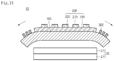
- FIGS. 10 and 11 are sectional views showing a touch window according to still another embodiment.
- the touch window includes first and second touch windows 11 and 12.
- Each of the first and second touch windows 11 and 12 may be identical to the touch window of FIG. 9 described above.
- the first touch window 11 may make contact with the second touch window 12 at second active areas 2AA provided at each side of the first and second touch windows 11 and 12. That is, the first and second touch windows 11 and 12 may be disposed to enable the second active areas 2AA to meet each other. Thus, a foldable touch window may be provided through the first and second touch windows 11 and 12. Meanwhile, referring to FIG. 11 , the touch window 10 may be combined with a driving part 20 and a light source part 30, so that a touch device may be implemented.
- the driving part 20 may be a display panel.
- a display region to output an image is formed in the display panel 20.
- a display panel applied to the touch device may generally include an upper substrate 21 and a lower substrate 22.
- a data line, a gate line and a thin-film transistor (TFT) may be formed in the lower substrate 22.
- the upper substrate 21 may be adhesive to the lower substrate 22 such that the elements provided on the lower substrate 22 may be protected.
- the display panel 20 may be formed in various types according to the type of touch device. That is, the touch device according to the embodiment may include a liquid-crystal device (LCD), a field emission display, a plasma display panel (PDP), an organic light-emitting diode (OLED), and an electronic paper display (EPD). Thus, the display panel 20 may be implemented in various types.
- LCD liquid-crystal device
- PDP plasma display panel
- OLED organic light-emitting diode
- EPD electronic paper display
- a touch window may include third and fourth touch windows 13 and 14.
- the third and fourth touch windows 13 and 14 may be combined with a driving part 20 and a light source part 30, so that a touch device may be implemented.
- the third and fourth touch windows 13 and 14 may be identical to the touch window of FIG. 7 .
- the third and fourth touch windows 13 and 14 may make contact with each other at the unactive areas UA thereof. That is, the third and fourth touch windows 13 and 14 may be disposed to enable the unactive areas UA to meet each other.
- the third and fourth touch windows 13 and 14 may be coupled through a coupling part 40 disposed between the third and fourth touch windows 13 and 14.
- a touch device which is foldable through the third and fourth touch windows 13 and 14, may be provided.
- various types of touch device may be implemented.
- the touch window may include a curved touch window.
- a touch device including the touch window may be a curved touch device.
- the first or second sensing electrode 210 or 220 may include a conductive pattern, so that the bending property and the reliability of the touch window may be improved.
- the touch window may include a flexible touch window.
- the display device may be flexible touch device. Therefore, a user may allow the display device to be flexible or bendable with his hand.
- the first or second sensing electrode 210 or 220 may include a conductive pattern, so that the bending property and the reliability of the touch window may be improved.
- the touch window may be applied to a vehicle as well as a touch device of a mobile terminal.
- the touch window may be applied to a dashboard as well as a personal navigation display (PND) of vehicle navigation, so that a center information display (CID) may be implemented.
- PND personal navigation display
- CID center information display
- any reference in this specification to "one embodiment,” “an embodiment,” “example embodiment,” etc., means that a particular feature, structure, or characteristic described in connection with the embodiment is included in at least one embodiment of the invention.
- the appearances of such phrases in various places in the specification are not necessarily all referring to the same embodiment.
Landscapes
- Engineering & Computer Science (AREA)
- Theoretical Computer Science (AREA)
- General Engineering & Computer Science (AREA)
- Human Computer Interaction (AREA)
- Physics & Mathematics (AREA)
- General Physics & Mathematics (AREA)
- Computer Hardware Design (AREA)
- Quality & Reliability (AREA)
- Position Input By Displaying (AREA)
Applications Claiming Priority (1)
| Application Number | Priority Date | Filing Date | Title |
|---|---|---|---|
| KR1020130089661A KR102008795B1 (ko) | 2013-07-29 | 2013-07-29 | 터치 윈도우 |
Publications (2)
| Publication Number | Publication Date |
|---|---|
| EP2833235A1 EP2833235A1 (en) | 2015-02-04 |
| EP2833235B1 true EP2833235B1 (en) | 2019-10-30 |
Family
ID=51212658
Family Applications (1)
| Application Number | Title | Priority Date | Filing Date |
|---|---|---|---|
| EP14172733.9A Active EP2833235B1 (en) | 2013-07-29 | 2014-06-17 | Flexible touch panel with bendable active area |
Country Status (6)
| Country | Link |
|---|---|
| US (1) | US9547397B2 (enExample) |
| EP (1) | EP2833235B1 (enExample) |
| JP (1) | JP6522894B2 (enExample) |
| KR (1) | KR102008795B1 (enExample) |
| CN (1) | CN104346015B (enExample) |
| TW (1) | TWI630517B (enExample) |
Families Citing this family (6)
| Publication number | Priority date | Publication date | Assignee | Title |
|---|---|---|---|---|
| KR20150024572A (ko) | 2013-08-27 | 2015-03-09 | 엘지이노텍 주식회사 | 터치 윈도우 및 이를 포함하는 디스플레이 |
| KR102183097B1 (ko) * | 2014-03-10 | 2020-11-25 | 엘지전자 주식회사 | 전도성 필름 및 이를 포함하는 터치 패널 |
| WO2015170677A1 (ja) * | 2014-05-08 | 2015-11-12 | シャープ株式会社 | 位置入力装置の製造方法 |
| JP6495748B2 (ja) * | 2015-06-05 | 2019-04-03 | 株式会社ジャパンディスプレイ | タッチ検出装置、タッチ検出機能付き表示装置及びカバー部材 |
| CN107017265A (zh) * | 2016-01-27 | 2017-08-04 | 上海和辉光电有限公司 | 一种柔性显示面板及其制备方法 |
| KR102517515B1 (ko) * | 2016-07-29 | 2023-04-04 | 삼성전자주식회사 | 입력 감지 패널을 구비한 전자 장치 |
Family Cites Families (27)
| Publication number | Priority date | Publication date | Assignee | Title |
|---|---|---|---|---|
| JP4747747B2 (ja) * | 2005-09-08 | 2011-08-17 | ソニー株式会社 | 入力装置、その製造方法及び電子機器 |
| CN101458602B (zh) * | 2007-12-12 | 2011-12-21 | 清华大学 | 触摸屏及显示装置 |
| JP4915954B2 (ja) * | 2007-11-27 | 2012-04-11 | グンゼ株式会社 | タッチパネルおよび該タッチパネルを使用したタッチパネル装置 |
| CN101470565B (zh) * | 2007-12-27 | 2011-08-24 | 清华大学 | 触摸屏及显示装置 |
| US9335868B2 (en) * | 2008-07-31 | 2016-05-10 | Apple Inc. | Capacitive sensor behind black mask |
| CN102473363B (zh) * | 2009-07-01 | 2014-08-27 | 夏普株式会社 | 显示装置 |
| US9632622B2 (en) * | 2009-07-16 | 2017-04-25 | Apple Inc. | Ground detection for touch sensitive device |
| CN101706698B (zh) * | 2009-11-23 | 2012-01-11 | 深圳市汇顶科技有限公司 | 一种触摸感应扫描检测方法、系统及电容型触摸传感器 |
| WO2011119707A2 (en) * | 2010-03-23 | 2011-09-29 | Cambrios Technologies Corporation | Etch patterning of nanostructure transparent conductors |
| CN101833121B (zh) * | 2010-04-09 | 2011-08-10 | 深圳市汇顶科技有限公司 | 一种双耦合型检测电路、雨量传感器及雨量识别方法 |
| KR101733485B1 (ko) * | 2010-06-15 | 2017-05-10 | 엘지전자 주식회사 | 터치 패널 및 이를 포함하는 이동 단말기 |
| JP2012033466A (ja) * | 2010-07-02 | 2012-02-16 | Fujifilm Corp | 導電層転写材料、及びタッチパネル |
| CN102004592A (zh) * | 2010-07-27 | 2011-04-06 | 苏州瀚瑞微电子有限公司 | 电容式触摸屏扫描方法 |
| US8717330B2 (en) * | 2010-11-22 | 2014-05-06 | Industrial Technology Research Institute | Flexible projective capacitive touch sensor structure |
| WO2012073929A1 (ja) * | 2010-12-02 | 2012-06-07 | シャープ株式会社 | 液晶表示装置およびマルチディスプレイシステム |
| CN202058129U (zh) * | 2010-12-29 | 2011-11-30 | 广东中显科技有限公司 | 多点触摸面板 |
| JP2012185797A (ja) * | 2011-02-15 | 2012-09-27 | Toshiba Corp | 電子機器 |
| WO2012132846A1 (ja) * | 2011-03-31 | 2012-10-04 | 日本写真印刷株式会社 | 静電容量方式のタッチスクリーン |
| EP2712284A4 (en) * | 2011-04-26 | 2014-11-05 | Nippon Mektron Kk | METHOD FOR PRODUCING A TRANSPARENT PRINTED PCB AND METHOD FOR PRODUCING A TRANSPARENT TOUCH SCREEN |
| CN102819334A (zh) * | 2011-06-09 | 2012-12-12 | 天津富纳源创科技有限公司 | 触摸屏 |
| TWI457808B (zh) * | 2011-06-09 | 2014-10-21 | Shih Hua Technology Ltd | 觸摸屏 |
| US8723824B2 (en) * | 2011-09-27 | 2014-05-13 | Apple Inc. | Electronic devices with sidewall displays |
| US20150027755A1 (en) * | 2011-12-19 | 2015-01-29 | Panasonic Corporation | Transparent conductive film, substrate carrying transparent conductive film, and production method thereof |
| JP5464617B2 (ja) * | 2012-01-12 | 2014-04-09 | 日本写真印刷株式会社 | 装飾付きタッチセンサ、及びその製造方法 |
| KR101357586B1 (ko) * | 2012-01-18 | 2014-02-05 | 엘지이노텍 주식회사 | 터치 패널 |
| TW201342442A (zh) * | 2012-04-10 | 2013-10-16 | Himax Tech Ltd | 觸控面板 |
| TW201409114A (zh) * | 2012-08-23 | 2014-03-01 | Henghao Technology Co Ltd | 觸控電極裝置 |
-
2013
- 2013-07-29 KR KR1020130089661A patent/KR102008795B1/ko active Active
-
2014
- 2014-06-06 TW TW103119748A patent/TWI630517B/zh active
- 2014-06-12 JP JP2014121633A patent/JP6522894B2/ja active Active
- 2014-06-17 EP EP14172733.9A patent/EP2833235B1/en active Active
- 2014-07-28 US US14/444,604 patent/US9547397B2/en active Active
- 2014-07-29 CN CN201410367802.6A patent/CN104346015B/zh active Active
Non-Patent Citations (1)
| Title |
|---|
| None * |
Also Published As
| Publication number | Publication date |
|---|---|
| US9547397B2 (en) | 2017-01-17 |
| KR20150014241A (ko) | 2015-02-06 |
| CN104346015A (zh) | 2015-02-11 |
| CN104346015B (zh) | 2019-02-22 |
| EP2833235A1 (en) | 2015-02-04 |
| TW201510810A (zh) | 2015-03-16 |
| KR102008795B1 (ko) | 2019-10-21 |
| TWI630517B (zh) | 2018-07-21 |
| US20150029150A1 (en) | 2015-01-29 |
| JP6522894B2 (ja) | 2019-05-29 |
| JP2015026370A (ja) | 2015-02-05 |
Similar Documents
| Publication | Publication Date | Title |
|---|---|---|
| CN104423708B (zh) | 触摸窗及包括触摸窗的触控装置 | |
| US9874985B2 (en) | Touch window | |
| EP2843519B1 (en) | Touch window and touch device including the same | |
| US9483132B2 (en) | Touch window and display including the same | |
| US10156944B2 (en) | Touch window | |
| EP2833235B1 (en) | Flexible touch panel with bendable active area | |
| US20150092359A1 (en) | Touch window and touch device with the same | |
| EP2833246B1 (en) | Touch window and touch device including the same | |
| US10055074B2 (en) | Touch window | |
| CN105874410B (zh) | 触摸窗和包含该触摸窗的显示设备 | |
| KR102199333B1 (ko) | 터치 윈도우 | |
| KR20150087943A (ko) | 터치 윈도우 및 이를 포함하는 디스플레이 | |
| KR102131177B1 (ko) | 터치 윈도우 및 이를 포함하는 디스플레이 장치 | |
| KR102119608B1 (ko) | 터치 윈도우 및 이를 포함하는 디스플레이 | |
| KR102187787B1 (ko) | 터치 윈도우 | |
| KR20160094813A (ko) | 터치 패널 | |
| KR20170001328A (ko) | 터치 윈도우 | |
| KR20170039391A (ko) | 터치 윈도우 |
Legal Events
| Date | Code | Title | Description |
|---|---|---|---|
| 17P | Request for examination filed |
Effective date: 20140617 |
|
| AK | Designated contracting states |
Kind code of ref document: A1 Designated state(s): AL AT BE BG CH CY CZ DE DK EE ES FI FR GB GR HR HU IE IS IT LI LT LU LV MC MK MT NL NO PL PT RO RS SE SI SK SM TR |
|
| AX | Request for extension of the european patent |
Extension state: BA ME |
|
| PUAI | Public reference made under article 153(3) epc to a published international application that has entered the european phase |
Free format text: ORIGINAL CODE: 0009012 |
|
| R17P | Request for examination filed (corrected) |
Effective date: 20150731 |
|
| RBV | Designated contracting states (corrected) |
Designated state(s): AL AT BE BG CH CY CZ DE DK EE ES FI FR GB GR HR HU IE IS IT LI LT LU LV MC MK MT NL NO PL PT RO RS SE SI SK SM TR |
|
| RAP1 | Party data changed (applicant data changed or rights of an application transferred) |
Owner name: LG INNOTEK CO., LTD. |
|
| STAA | Information on the status of an ep patent application or granted ep patent |
Free format text: STATUS: EXAMINATION IS IN PROGRESS |
|
| 17Q | First examination report despatched |
Effective date: 20180403 |
|
| GRAP | Despatch of communication of intention to grant a patent |
Free format text: ORIGINAL CODE: EPIDOSNIGR1 |
|
| STAA | Information on the status of an ep patent application or granted ep patent |
Free format text: STATUS: GRANT OF PATENT IS INTENDED |
|
| INTG | Intention to grant announced |
Effective date: 20190612 |
|
| GRAS | Grant fee paid |
Free format text: ORIGINAL CODE: EPIDOSNIGR3 |
|
| GRAA | (expected) grant |
Free format text: ORIGINAL CODE: 0009210 |
|
| STAA | Information on the status of an ep patent application or granted ep patent |
Free format text: STATUS: THE PATENT HAS BEEN GRANTED |
|
| AK | Designated contracting states |
Kind code of ref document: B1 Designated state(s): AL AT BE BG CH CY CZ DE DK EE ES FI FR GB GR HR HU IE IS IT LI LT LU LV MC MK MT NL NO PL PT RO RS SE SI SK SM TR |
|
| REG | Reference to a national code |
Ref country code: GB Ref legal event code: FG4D |
|
| REG | Reference to a national code |
Ref country code: CH Ref legal event code: EP |
|
| REG | Reference to a national code |
Ref country code: AT Ref legal event code: REF Ref document number: 1196834 Country of ref document: AT Kind code of ref document: T Effective date: 20191115 |
|
| REG | Reference to a national code |
Ref country code: DE Ref legal event code: R096 Ref document number: 602014055841 Country of ref document: DE |
|
| REG | Reference to a national code |
Ref country code: IE Ref legal event code: FG4D |
|
| REG | Reference to a national code |
Ref country code: LT Ref legal event code: MG4D |
|
| PG25 | Lapsed in a contracting state [announced via postgrant information from national office to epo] |
Ref country code: LT Free format text: LAPSE BECAUSE OF FAILURE TO SUBMIT A TRANSLATION OF THE DESCRIPTION OR TO PAY THE FEE WITHIN THE PRESCRIBED TIME-LIMIT Effective date: 20191030 Ref country code: GR Free format text: LAPSE BECAUSE OF FAILURE TO SUBMIT A TRANSLATION OF THE DESCRIPTION OR TO PAY THE FEE WITHIN THE PRESCRIBED TIME-LIMIT Effective date: 20200131 Ref country code: PL Free format text: LAPSE BECAUSE OF FAILURE TO SUBMIT A TRANSLATION OF THE DESCRIPTION OR TO PAY THE FEE WITHIN THE PRESCRIBED TIME-LIMIT Effective date: 20191030 Ref country code: NO Free format text: LAPSE BECAUSE OF FAILURE TO SUBMIT A TRANSLATION OF THE DESCRIPTION OR TO PAY THE FEE WITHIN THE PRESCRIBED TIME-LIMIT Effective date: 20200130 Ref country code: SE Free format text: LAPSE BECAUSE OF FAILURE TO SUBMIT A TRANSLATION OF THE DESCRIPTION OR TO PAY THE FEE WITHIN THE PRESCRIBED TIME-LIMIT Effective date: 20191030 Ref country code: LV Free format text: LAPSE BECAUSE OF FAILURE TO SUBMIT A TRANSLATION OF THE DESCRIPTION OR TO PAY THE FEE WITHIN THE PRESCRIBED TIME-LIMIT Effective date: 20191030 Ref country code: BG Free format text: LAPSE BECAUSE OF FAILURE TO SUBMIT A TRANSLATION OF THE DESCRIPTION OR TO PAY THE FEE WITHIN THE PRESCRIBED TIME-LIMIT Effective date: 20200130 Ref country code: FI Free format text: LAPSE BECAUSE OF FAILURE TO SUBMIT A TRANSLATION OF THE DESCRIPTION OR TO PAY THE FEE WITHIN THE PRESCRIBED TIME-LIMIT Effective date: 20191030 Ref country code: PT Free format text: LAPSE BECAUSE OF FAILURE TO SUBMIT A TRANSLATION OF THE DESCRIPTION OR TO PAY THE FEE WITHIN THE PRESCRIBED TIME-LIMIT Effective date: 20200302 Ref country code: NL Free format text: LAPSE BECAUSE OF FAILURE TO SUBMIT A TRANSLATION OF THE DESCRIPTION OR TO PAY THE FEE WITHIN THE PRESCRIBED TIME-LIMIT Effective date: 20191030 Ref country code: ES Free format text: LAPSE BECAUSE OF FAILURE TO SUBMIT A TRANSLATION OF THE DESCRIPTION OR TO PAY THE FEE WITHIN THE PRESCRIBED TIME-LIMIT Effective date: 20191030 |
|
| REG | Reference to a national code |
Ref country code: NL Ref legal event code: MP Effective date: 20191030 |
|
| PG25 | Lapsed in a contracting state [announced via postgrant information from national office to epo] |
Ref country code: IS Free format text: LAPSE BECAUSE OF FAILURE TO SUBMIT A TRANSLATION OF THE DESCRIPTION OR TO PAY THE FEE WITHIN THE PRESCRIBED TIME-LIMIT Effective date: 20200229 Ref country code: HR Free format text: LAPSE BECAUSE OF FAILURE TO SUBMIT A TRANSLATION OF THE DESCRIPTION OR TO PAY THE FEE WITHIN THE PRESCRIBED TIME-LIMIT Effective date: 20191030 Ref country code: RS Free format text: LAPSE BECAUSE OF FAILURE TO SUBMIT A TRANSLATION OF THE DESCRIPTION OR TO PAY THE FEE WITHIN THE PRESCRIBED TIME-LIMIT Effective date: 20191030 |
|
| PG25 | Lapsed in a contracting state [announced via postgrant information from national office to epo] |
Ref country code: AL Free format text: LAPSE BECAUSE OF FAILURE TO SUBMIT A TRANSLATION OF THE DESCRIPTION OR TO PAY THE FEE WITHIN THE PRESCRIBED TIME-LIMIT Effective date: 20191030 |
|
| PG25 | Lapsed in a contracting state [announced via postgrant information from national office to epo] |
Ref country code: RO Free format text: LAPSE BECAUSE OF FAILURE TO SUBMIT A TRANSLATION OF THE DESCRIPTION OR TO PAY THE FEE WITHIN THE PRESCRIBED TIME-LIMIT Effective date: 20191030 Ref country code: CZ Free format text: LAPSE BECAUSE OF FAILURE TO SUBMIT A TRANSLATION OF THE DESCRIPTION OR TO PAY THE FEE WITHIN THE PRESCRIBED TIME-LIMIT Effective date: 20191030 Ref country code: EE Free format text: LAPSE BECAUSE OF FAILURE TO SUBMIT A TRANSLATION OF THE DESCRIPTION OR TO PAY THE FEE WITHIN THE PRESCRIBED TIME-LIMIT Effective date: 20191030 Ref country code: DK Free format text: LAPSE BECAUSE OF FAILURE TO SUBMIT A TRANSLATION OF THE DESCRIPTION OR TO PAY THE FEE WITHIN THE PRESCRIBED TIME-LIMIT Effective date: 20191030 |
|
| REG | Reference to a national code |
Ref country code: DE Ref legal event code: R097 Ref document number: 602014055841 Country of ref document: DE |
|
| REG | Reference to a national code |
Ref country code: AT Ref legal event code: MK05 Ref document number: 1196834 Country of ref document: AT Kind code of ref document: T Effective date: 20191030 |
|
| PG25 | Lapsed in a contracting state [announced via postgrant information from national office to epo] |
Ref country code: IT Free format text: LAPSE BECAUSE OF FAILURE TO SUBMIT A TRANSLATION OF THE DESCRIPTION OR TO PAY THE FEE WITHIN THE PRESCRIBED TIME-LIMIT Effective date: 20191030 Ref country code: SM Free format text: LAPSE BECAUSE OF FAILURE TO SUBMIT A TRANSLATION OF THE DESCRIPTION OR TO PAY THE FEE WITHIN THE PRESCRIBED TIME-LIMIT Effective date: 20191030 Ref country code: SK Free format text: LAPSE BECAUSE OF FAILURE TO SUBMIT A TRANSLATION OF THE DESCRIPTION OR TO PAY THE FEE WITHIN THE PRESCRIBED TIME-LIMIT Effective date: 20191030 |
|
| PLBE | No opposition filed within time limit |
Free format text: ORIGINAL CODE: 0009261 |
|
| STAA | Information on the status of an ep patent application or granted ep patent |
Free format text: STATUS: NO OPPOSITION FILED WITHIN TIME LIMIT |
|
| 26N | No opposition filed |
Effective date: 20200731 |
|
| PG25 | Lapsed in a contracting state [announced via postgrant information from national office to epo] |
Ref country code: AT Free format text: LAPSE BECAUSE OF FAILURE TO SUBMIT A TRANSLATION OF THE DESCRIPTION OR TO PAY THE FEE WITHIN THE PRESCRIBED TIME-LIMIT Effective date: 20191030 Ref country code: SI Free format text: LAPSE BECAUSE OF FAILURE TO SUBMIT A TRANSLATION OF THE DESCRIPTION OR TO PAY THE FEE WITHIN THE PRESCRIBED TIME-LIMIT Effective date: 20191030 |
|
| PG25 | Lapsed in a contracting state [announced via postgrant information from national office to epo] |
Ref country code: MC Free format text: LAPSE BECAUSE OF FAILURE TO SUBMIT A TRANSLATION OF THE DESCRIPTION OR TO PAY THE FEE WITHIN THE PRESCRIBED TIME-LIMIT Effective date: 20191030 |
|
| REG | Reference to a national code |
Ref country code: CH Ref legal event code: PL |
|
| GBPC | Gb: european patent ceased through non-payment of renewal fee |
Effective date: 20200617 |
|
| PG25 | Lapsed in a contracting state [announced via postgrant information from national office to epo] |
Ref country code: LU Free format text: LAPSE BECAUSE OF NON-PAYMENT OF DUE FEES Effective date: 20200617 |
|
| REG | Reference to a national code |
Ref country code: BE Ref legal event code: MM Effective date: 20200630 |
|
| PG25 | Lapsed in a contracting state [announced via postgrant information from national office to epo] |
Ref country code: CH Free format text: LAPSE BECAUSE OF NON-PAYMENT OF DUE FEES Effective date: 20200630 Ref country code: GB Free format text: LAPSE BECAUSE OF NON-PAYMENT OF DUE FEES Effective date: 20200617 Ref country code: IE Free format text: LAPSE BECAUSE OF NON-PAYMENT OF DUE FEES Effective date: 20200617 Ref country code: LI Free format text: LAPSE BECAUSE OF NON-PAYMENT OF DUE FEES Effective date: 20200630 Ref country code: FR Free format text: LAPSE BECAUSE OF NON-PAYMENT OF DUE FEES Effective date: 20200630 |
|
| PG25 | Lapsed in a contracting state [announced via postgrant information from national office to epo] |
Ref country code: BE Free format text: LAPSE BECAUSE OF NON-PAYMENT OF DUE FEES Effective date: 20200630 |
|
| PGFP | Annual fee paid to national office [announced via postgrant information from national office to epo] |
Ref country code: DE Payment date: 20210520 Year of fee payment: 8 |
|
| PG25 | Lapsed in a contracting state [announced via postgrant information from national office to epo] |
Ref country code: TR Free format text: LAPSE BECAUSE OF FAILURE TO SUBMIT A TRANSLATION OF THE DESCRIPTION OR TO PAY THE FEE WITHIN THE PRESCRIBED TIME-LIMIT Effective date: 20191030 Ref country code: MT Free format text: LAPSE BECAUSE OF FAILURE TO SUBMIT A TRANSLATION OF THE DESCRIPTION OR TO PAY THE FEE WITHIN THE PRESCRIBED TIME-LIMIT Effective date: 20191030 Ref country code: CY Free format text: LAPSE BECAUSE OF FAILURE TO SUBMIT A TRANSLATION OF THE DESCRIPTION OR TO PAY THE FEE WITHIN THE PRESCRIBED TIME-LIMIT Effective date: 20191030 |
|
| PG25 | Lapsed in a contracting state [announced via postgrant information from national office to epo] |
Ref country code: MK Free format text: LAPSE BECAUSE OF FAILURE TO SUBMIT A TRANSLATION OF THE DESCRIPTION OR TO PAY THE FEE WITHIN THE PRESCRIBED TIME-LIMIT Effective date: 20191030 |
|
| REG | Reference to a national code |
Ref country code: DE Ref legal event code: R119 Ref document number: 602014055841 Country of ref document: DE |
|
| PG25 | Lapsed in a contracting state [announced via postgrant information from national office to epo] |
Ref country code: DE Free format text: LAPSE BECAUSE OF NON-PAYMENT OF DUE FEES Effective date: 20230103 |