EP2826059B1 - Procédé d'impression, appareil d'impression et procédé de fabrication d'article - Google Patents
Procédé d'impression, appareil d'impression et procédé de fabrication d'article Download PDFInfo
- Publication number
- EP2826059B1 EP2826059B1 EP13760289.2A EP13760289A EP2826059B1 EP 2826059 B1 EP2826059 B1 EP 2826059B1 EP 13760289 A EP13760289 A EP 13760289A EP 2826059 B1 EP2826059 B1 EP 2826059B1
- Authority
- EP
- European Patent Office
- Prior art keywords
- imprint
- mold
- substrate
- detector
- pattern
- Prior art date
- Legal status (The legal status is an assumption and is not a legal conclusion. Google has not performed a legal analysis and makes no representation as to the accuracy of the status listed.)
- Active
Links
- 238000000034 method Methods 0.000 title claims description 28
- 238000004519 manufacturing process Methods 0.000 title claims description 13
- 239000000758 substrate Substances 0.000 claims description 42
- 238000012545 processing Methods 0.000 claims description 31
- 239000000463 material Substances 0.000 claims description 26
- 238000001514 detection method Methods 0.000 claims description 19
- 230000008859 change Effects 0.000 claims description 5
- 239000011347 resin Substances 0.000 description 49
- 229920005989 resin Polymers 0.000 description 49
- 230000007246 mechanism Effects 0.000 description 38
- 238000003825 pressing Methods 0.000 description 25
- 230000002093 peripheral effect Effects 0.000 description 19
- 238000012937 correction Methods 0.000 description 9
- 238000010586 diagram Methods 0.000 description 8
- 238000005259 measurement Methods 0.000 description 7
- 230000003287 optical effect Effects 0.000 description 6
- 238000001723 curing Methods 0.000 description 5
- 238000005516 engineering process Methods 0.000 description 5
- 230000008569 process Effects 0.000 description 5
- VYPSYNLAJGMNEJ-UHFFFAOYSA-N silicon dioxide Inorganic materials O=[Si]=O VYPSYNLAJGMNEJ-UHFFFAOYSA-N 0.000 description 5
- 238000000016 photochemical curing Methods 0.000 description 3
- 239000004065 semiconductor Substances 0.000 description 3
- 230000008901 benefit Effects 0.000 description 2
- 238000005530 etching Methods 0.000 description 2
- 239000011521 glass Substances 0.000 description 2
- 238000009434 installation Methods 0.000 description 2
- XUIMIQQOPSSXEZ-UHFFFAOYSA-N Silicon Chemical compound [Si] XUIMIQQOPSSXEZ-UHFFFAOYSA-N 0.000 description 1
- 230000002411 adverse Effects 0.000 description 1
- 238000011161 development Methods 0.000 description 1
- 230000018109 developmental process Effects 0.000 description 1
- 238000007599 discharging Methods 0.000 description 1
- 238000006073 displacement reaction Methods 0.000 description 1
- 230000000694 effects Effects 0.000 description 1
- 239000012530 fluid Substances 0.000 description 1
- 229910052736 halogen Inorganic materials 0.000 description 1
- 150000002367 halogens Chemical class 0.000 description 1
- 238000010438 heat treatment Methods 0.000 description 1
- 238000005286 illumination Methods 0.000 description 1
- 239000012212 insulator Substances 0.000 description 1
- 230000001678 irradiating effect Effects 0.000 description 1
- 239000007788 liquid Substances 0.000 description 1
- 238000012986 modification Methods 0.000 description 1
- 230000004048 modification Effects 0.000 description 1
- 229910021421 monocrystalline silicon Inorganic materials 0.000 description 1
- 239000003921 oil Substances 0.000 description 1
- 238000000206 photolithography Methods 0.000 description 1
- 230000002035 prolonged effect Effects 0.000 description 1
- 239000010453 quartz Substances 0.000 description 1
- 229910052710 silicon Inorganic materials 0.000 description 1
- 239000010703 silicon Substances 0.000 description 1
- 238000003860 storage Methods 0.000 description 1
Images


Classifications
-
- H—ELECTRICITY
- H01—ELECTRIC ELEMENTS
- H01L—SEMICONDUCTOR DEVICES NOT COVERED BY CLASS H10
- H01L21/00—Processes or apparatus adapted for the manufacture or treatment of semiconductor or solid state devices or of parts thereof
- H01L21/02—Manufacture or treatment of semiconductor devices or of parts thereof
- H01L21/027—Making masks on semiconductor bodies for further photolithographic processing not provided for in group H01L21/18 or H01L21/34
- H01L21/0271—Making masks on semiconductor bodies for further photolithographic processing not provided for in group H01L21/18 or H01L21/34 comprising organic layers
- H01L21/0273—Making masks on semiconductor bodies for further photolithographic processing not provided for in group H01L21/18 or H01L21/34 comprising organic layers characterised by the treatment of photoresist layers
- H01L21/0274—Photolithographic processes
-
- G—PHYSICS
- G03—PHOTOGRAPHY; CINEMATOGRAPHY; ANALOGOUS TECHNIQUES USING WAVES OTHER THAN OPTICAL WAVES; ELECTROGRAPHY; HOLOGRAPHY
- G03F—PHOTOMECHANICAL PRODUCTION OF TEXTURED OR PATTERNED SURFACES, e.g. FOR PRINTING, FOR PROCESSING OF SEMICONDUCTOR DEVICES; MATERIALS THEREFOR; ORIGINALS THEREFOR; APPARATUS SPECIALLY ADAPTED THEREFOR
- G03F7/00—Photomechanical, e.g. photolithographic, production of textured or patterned surfaces, e.g. printing surfaces; Materials therefor, e.g. comprising photoresists; Apparatus specially adapted therefor
- G03F7/0002—Lithographic processes using patterning methods other than those involving the exposure to radiation, e.g. by stamping
-
- G—PHYSICS
- G03—PHOTOGRAPHY; CINEMATOGRAPHY; ANALOGOUS TECHNIQUES USING WAVES OTHER THAN OPTICAL WAVES; ELECTROGRAPHY; HOLOGRAPHY
- G03F—PHOTOMECHANICAL PRODUCTION OF TEXTURED OR PATTERNED SURFACES, e.g. FOR PRINTING, FOR PROCESSING OF SEMICONDUCTOR DEVICES; MATERIALS THEREFOR; ORIGINALS THEREFOR; APPARATUS SPECIALLY ADAPTED THEREFOR
- G03F9/00—Registration or positioning of originals, masks, frames, photographic sheets or textured or patterned surfaces, e.g. automatically
- G03F9/70—Registration or positioning of originals, masks, frames, photographic sheets or textured or patterned surfaces, e.g. automatically for microlithography
- G03F9/7003—Alignment type or strategy, e.g. leveling, global alignment
- G03F9/7038—Alignment for proximity or contact printer
-
- G—PHYSICS
- G03—PHOTOGRAPHY; CINEMATOGRAPHY; ANALOGOUS TECHNIQUES USING WAVES OTHER THAN OPTICAL WAVES; ELECTROGRAPHY; HOLOGRAPHY
- G03F—PHOTOMECHANICAL PRODUCTION OF TEXTURED OR PATTERNED SURFACES, e.g. FOR PRINTING, FOR PROCESSING OF SEMICONDUCTOR DEVICES; MATERIALS THEREFOR; ORIGINALS THEREFOR; APPARATUS SPECIALLY ADAPTED THEREFOR
- G03F9/00—Registration or positioning of originals, masks, frames, photographic sheets or textured or patterned surfaces, e.g. automatically
- G03F9/70—Registration or positioning of originals, masks, frames, photographic sheets or textured or patterned surfaces, e.g. automatically for microlithography
- G03F9/7088—Alignment mark detection, e.g. TTR, TTL, off-axis detection, array detector, video detection
Claims (11)
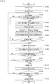
- Procédé d'impression pour amener un matériau d'impression sur un substrat en contact avec un moule afin de former un motif du matériau d'impression, le procédé d'impression comprenant les étapes consistant à :modifier une position d'un détecteur qui détecte un repère d'alignement formé sur une région de charge d'injection sur le substrat (S103, S107) ;mettre le moule en contact avec le matériau d'impression distribué sur la région de charge d'injection sur le substrat (S106, S111) ; etdétecter le repère d'alignement en utilisant le détecteur une fois terminée la modification de la position du détecteur (S108),caractérisé en ce quela modification de la position du détecteur est débutée (S103) avant la mise en contact du moule avec le matériau d'impression (S106), etla mise en contact est débutée (S106) avant de terminer (S107) la modification de la position du détecteur.
- Procédé d'impression selon la revendication 1, dans lequel la mise en contact est débutée sur la base du résultat de détection obtenu en détectant un repère d'alignement par rapport à une autre région de charge d'injection à laquelle le motif est transféré sur le matériau d'impression.
- Procédé d'impression selon la revendication 1, le procédé d'impression transférant, de manière répétée, un motif formé sur le moule sur une pluralité de régions de charge d'injection formées sur le substrat, et la modification de la position du détecteur visant à changer la position du détecteur depuis la position d'une région de charge d'injection sur laquelle le motif formé sur le moule a été transféré jusqu'à la position de la région de charge d'injection suivante sur le substrat sur lequel le motif doit être transféré.
- Procédé d'impression selon la revendication 1, dans lequel lorsque le détecteur est fourni en pluralité et que le détecteur dont la position est modifiée au cours de la modification de la position du détecteur et le détecteur dont la position n'est pas modifiée existent, le détecteur dont la position n'est pas modifiée débute la mise en contact du moule en détectant le repère d'alignement et le détecteur dont la position est modifiée détecte le repère d'alignement une fois terminée la modification de la position du détecteur dont la position est modifiée.
- Procédé d'impression selon la revendication 1, comprenant, en outre, les étapes consistant à :durcir le matériau d'impression non durci sur la région de charge d'injection une fois terminée la mise en contact ;libérer le moule du matériau d'impression durci ; etdétecter un repère d'alignement formé sur la région de charge d'injection devant être ensuite traitée avant le durcissement ou la libération après avoir terminé au moins l'une des étapes parmi la mise en correspondance de la forme du motif formé sur le moule avec la forme de la région de charge d'injection et l'alignement du moule avec le substrat.
- Procédé d'impression pour amener un matériau d'impression sur un substrat en contact avec un moule afin de former un motif du matériau d'impression, le procédé d'impression comprenant les étapes consistant à :distribuer le matériau d'impression sur le substrat (S104) ;modifier la position d'un détecteur qui détecte un repère d'alignement formé sur une région de charge d'injection sur le substrat (S103, S107) ;mettre le moule en contact avec le matériau d'impression distribué sur la région de charge d'injection sur le substrat (S106, S111) ; etdétecter le repère d'alignement en utilisant le détecteur une fois terminée la modification de la position du détecteur (108),caractérisé en ce quela distribution du matériau d'impression (S104) est réalisée au cours de la modification de la position du détecteur (S103, S107).
- Appareil d'impression configuré pour amener un matériau d'impression (R) sur un substrat (W) en contact avec un moule (M) afin de former un motif du matériau d'impression, l'appareil d'impression comprenant :un détecteur (19) configuré pour détecter un repère d'alignement (AMM, AMW), parmi une pluralité de repères d'alignement formés sur une région de charge d'injection sur le substrat, afin de permettre à la position de détection du repère d'alignement d'être modifiée ; etcaractérisé en ce qu'il comprend en outre :
un dispositif de commande (7) configuré pour débuter la modification de la position du détecteur avant de mettre en contact le moule avec le matériau d'impression et pour débuter à amener le moule en contact avec le matériau d'impression distribué sur la région de charge d'injection sur le substrat avant de terminer la modification de la position du détecteur. - Procédé de fabrication d'article comprenant les étapes consistant à :former un motif de matériau d'impression sur un substrat en utilisant le procédé d'impression selon la revendication 1 ; ettraiter le substrat sur lequel le motif a été formé au cours de la formation.
- Procédé de fabrication d'article comprenant les étapes consistant à :former un motif de matériau d'impression sur un substrat en utilisant le procédé d'impression selon la revendication 6 ; ettraiter le substrat sur lequel le motif a été formé au cours de la formation.
- Procédé de fabrication d'article comprenant les étapes consistant à :former un motif de matériau d'impression sur un substrat en utilisant l'appareil d'impression selon la revendication 7 ; ettraiter le substrat sur lequel le motif a été formé au cours de la formation.
- Appareil d'impression configuré pour amener un matériau d'impression (R) sur un substrat (W) en contact avec un moule (M) afin de former un motif du matériau d'impression, l'appareil d'impression comprenant :un détecteur (19) configuré pour détecter un repère d'alignement (AMM, AMW), parmi une pluralité de repères d'alignement formés sur une région de charge d'injection sur le substrat, afin de permettre à la position de détection du repère d'alignement d'être modifiée ;caractérisé en ce qu'il comprend en outre :
un dispositif de commande (7) configuré pour distribuer le matériau d'impression sur la région de charge d'injection sur le substrat au cours de la modification de la position du détecteur.
Applications Claiming Priority (3)
| Application Number | Priority Date | Filing Date | Title |
|---|---|---|---|
| JP2012053991 | 2012-03-12 | ||
| JP2013042700A JP6029495B2 (ja) | 2012-03-12 | 2013-03-05 | インプリント方法およびインプリント装置、それを用いた物品の製造方法 |
| PCT/JP2013/001446 WO2013136733A1 (fr) | 2012-03-12 | 2013-03-07 | Procédé d'impression, appareil d'impression et procédé de fabrication d'article |
Publications (3)
| Publication Number | Publication Date |
|---|---|
| EP2826059A1 EP2826059A1 (fr) | 2015-01-21 |
| EP2826059A4 EP2826059A4 (fr) | 2015-11-18 |
| EP2826059B1 true EP2826059B1 (fr) | 2019-10-09 |
Family
ID=49160666
Family Applications (1)
| Application Number | Title | Priority Date | Filing Date |
|---|---|---|---|
| EP13760289.2A Active EP2826059B1 (fr) | 2012-03-12 | 2013-03-07 | Procédé d'impression, appareil d'impression et procédé de fabrication d'article |
Country Status (6)
| Country | Link |
|---|---|
| US (1) | US9703190B2 (fr) |
| EP (1) | EP2826059B1 (fr) |
| JP (1) | JP6029495B2 (fr) |
| KR (1) | KR101674279B1 (fr) |
| CN (1) | CN104160476B (fr) |
| WO (1) | WO2013136733A1 (fr) |
Families Citing this family (14)
| Publication number | Priority date | Publication date | Assignee | Title |
|---|---|---|---|---|
| JP6097704B2 (ja) | 2014-01-06 | 2017-03-15 | キヤノン株式会社 | インプリント装置、インプリント方法及び物品の製造方法 |
| JP6294680B2 (ja) * | 2014-01-24 | 2018-03-14 | キヤノン株式会社 | インプリント装置、および物品の製造方法 |
| JP2015170815A (ja) | 2014-03-10 | 2015-09-28 | キヤノン株式会社 | インプリント装置、アライメント方法及び物品の製造方法 |
| JP6401501B2 (ja) * | 2014-06-02 | 2018-10-10 | キヤノン株式会社 | インプリント装置、および物品の製造方法 |
| JP2016134441A (ja) * | 2015-01-16 | 2016-07-25 | キヤノン株式会社 | インプリント装置、インプリント方法、および物品の製造方法 |
| EP3291011A4 (fr) * | 2015-03-25 | 2019-02-27 | Nikon Corporation | Procédé de disposition, procédé de détection de marques, procédé d'exposition à la lumière, appareil de mesure, appareil d'exposition à la lumière, et procédé de fabrication de dispositif |
| TWI619145B (zh) * | 2015-04-30 | 2018-03-21 | 佳能股份有限公司 | 壓印裝置,基板運送裝置,壓印方法以及製造物件的方法 |
| JP6685821B2 (ja) * | 2016-04-25 | 2020-04-22 | キヤノン株式会社 | 計測装置、インプリント装置、物品の製造方法、光量決定方法、及び、光量調整方法 |
| JP6865650B2 (ja) * | 2017-07-27 | 2021-04-28 | キヤノン株式会社 | インプリント装置、および物品製造方法 |
| US10788749B2 (en) | 2017-11-30 | 2020-09-29 | Canon Kabushiki Kaisha | System and method for improving the throughput of a nanoimprint system |
| JP7317575B2 (ja) * | 2019-05-28 | 2023-07-31 | キヤノン株式会社 | インプリント装置、インプリント方法、および物品の製造方法 |
| JP7433861B2 (ja) | 2019-11-27 | 2024-02-20 | キヤノン株式会社 | インプリント装置、インプリント方法、物品の製造方法、基板、および、型 |
| US11966157B2 (en) * | 2021-05-20 | 2024-04-23 | Canon Kabushiki Kaisha | Imprint apparatus, imprint method, and article manufacturing method |
| JP2023040493A (ja) * | 2021-09-10 | 2023-03-23 | キヤノン株式会社 | インプリント装置、インプリント方法、及び物品の製造方法 |
Family Cites Families (10)
| Publication number | Priority date | Publication date | Assignee | Title |
|---|---|---|---|---|
| JP2006165371A (ja) * | 2004-12-09 | 2006-06-22 | Canon Inc | 転写装置およびデバイス製造方法 |
| JP4827513B2 (ja) | 2005-12-09 | 2011-11-30 | キヤノン株式会社 | 加工方法 |
| JP4185941B2 (ja) * | 2006-04-04 | 2008-11-26 | キヤノン株式会社 | ナノインプリント方法及びナノインプリント装置 |
| KR101238137B1 (ko) * | 2007-02-06 | 2013-02-28 | 캐논 가부시끼가이샤 | 임프린트 방법 및 임프린트 장치 |
| JP5279397B2 (ja) * | 2008-08-06 | 2013-09-04 | キヤノン株式会社 | インプリント装置、インプリント方法、およびデバイス製造方法 |
| NL2003871A (en) * | 2009-02-04 | 2010-08-05 | Asml Netherlands Bv | Imprint lithography. |
| JP5495767B2 (ja) * | 2009-12-21 | 2014-05-21 | キヤノン株式会社 | インプリント装置及び方法、並びに物品の製造方法 |
| JP5539011B2 (ja) * | 2010-05-14 | 2014-07-02 | キヤノン株式会社 | インプリント装置、検出装置、位置合わせ装置、及び物品の製造方法 |
| JP5597031B2 (ja) * | 2010-05-31 | 2014-10-01 | キヤノン株式会社 | リソグラフィ装置及び物品の製造方法 |
| JP5247777B2 (ja) * | 2010-08-30 | 2013-07-24 | キヤノン株式会社 | インプリント装置およびデバイス製造方法 |
-
2013
- 2013-03-05 JP JP2013042700A patent/JP6029495B2/ja active Active
- 2013-03-07 CN CN201380013069.1A patent/CN104160476B/zh active Active
- 2013-03-07 WO PCT/JP2013/001446 patent/WO2013136733A1/fr active Application Filing
- 2013-03-07 KR KR1020147025332A patent/KR101674279B1/ko active IP Right Grant
- 2013-03-07 EP EP13760289.2A patent/EP2826059B1/fr active Active
- 2013-03-07 US US14/380,797 patent/US9703190B2/en active Active
Non-Patent Citations (1)
| Title |
|---|
| None * |
Also Published As
| Publication number | Publication date |
|---|---|
| US9703190B2 (en) | 2017-07-11 |
| EP2826059A4 (fr) | 2015-11-18 |
| US20150013559A1 (en) | 2015-01-15 |
| KR20140124836A (ko) | 2014-10-27 |
| CN104160476A (zh) | 2014-11-19 |
| WO2013136733A1 (fr) | 2013-09-19 |
| EP2826059A1 (fr) | 2015-01-21 |
| CN104160476B (zh) | 2017-03-08 |
| JP6029495B2 (ja) | 2016-11-24 |
| JP2013219333A (ja) | 2013-10-24 |
| KR101674279B1 (ko) | 2016-11-08 |
Similar Documents
| Publication | Publication Date | Title |
|---|---|---|
| EP2826059B1 (fr) | Procédé d'impression, appareil d'impression et procédé de fabrication d'article | |
| EP2791966B1 (fr) | Procédé d'impression, appareil d'impression et procédé de fabrication d'article les mettant en oeuvre | |
| KR101625706B1 (ko) | 임프린트 장치, 이를 이용한 물품의 제조 방법 및 임프린트 방법 | |
| US10105892B2 (en) | Imprint apparatus and imprint method, and article manufacturing method | |
| US9594301B2 (en) | Imprint apparatus and article manufacturing method using same | |
| JP2021057612A (ja) | インプリント装置、インプリント方法および物品の製造方法 | |
| US10018910B2 (en) | Imprint apparatus, alignment method, and method of manufacturing article | |
| JP5662741B2 (ja) | インプリント装置および物品の製造方法 | |
| US9851634B2 (en) | Imprint apparatus | |
| KR101777905B1 (ko) | 임프린트 장치 그리고 물품을 제조하는 방법 | |
| US9971256B2 (en) | Imprint apparatus, imprint method, and method of manufacturing article | |
| JP6306830B2 (ja) | インプリント装置、および物品の製造方法 | |
| TWI720301B (zh) | 壓印裝置及製造物品的方法 | |
| KR20160140485A (ko) | 몰드, 임프린트 방법 및 임프린트 장치, 및 물품의 제조 방법 | |
| JP2015111708A (ja) | インプリント装置、インプリント方法、及びデバイス製造方法 | |
| JP2013225616A (ja) | インプリント方法、それを用いた物品の製造方法 | |
| US20230061381A1 (en) | Imprint apparatus and article manufacturing method | |
| US20230083496A1 (en) | Imprint apparatus, method of imprinting, and method of manufacturing article | |
| JP2017183364A (ja) | インプリント方法、インプリント装置、プログラム、および物品の製造方法 | |
| KR20160007377A (ko) | 임프린트 장치 및 물품 제조 방법 |
Legal Events
| Date | Code | Title | Description |
|---|---|---|---|
| PUAI | Public reference made under article 153(3) epc to a published international application that has entered the european phase |
Free format text: ORIGINAL CODE: 0009012 |
|
| 17P | Request for examination filed |
Effective date: 20140820 |
|
| AK | Designated contracting states |
Kind code of ref document: A1 Designated state(s): AL AT BE BG CH CY CZ DE DK EE ES FI FR GB GR HR HU IE IS IT LI LT LU LV MC MK MT NL NO PL PT RO RS SE SI SK SM TR |
|
| AX | Request for extension of the european patent |
Extension state: BA ME |
|
| DAX | Request for extension of the european patent (deleted) | ||
| RA4 | Supplementary search report drawn up and despatched (corrected) |
Effective date: 20151021 |
|
| RIC1 | Information provided on ipc code assigned before grant |
Ipc: H01L 21/027 20060101AFI20151015BHEP Ipc: G03F 7/00 20060101ALI20151015BHEP Ipc: G03F 9/00 20060101ALI20151015BHEP Ipc: B29C 59/02 20060101ALI20151015BHEP |
|
| REG | Reference to a national code |
Ref country code: DE Ref legal event code: R079 Ref document number: 602013061488 Country of ref document: DE Free format text: PREVIOUS MAIN CLASS: H01L0021027000 Ipc: G03F0007000000 |
|
| RIC1 | Information provided on ipc code assigned before grant |
Ipc: H01L 21/027 20060101ALI20170126BHEP Ipc: B29C 59/02 20060101ALI20170126BHEP Ipc: G03F 7/00 20060101AFI20170126BHEP Ipc: G03F 9/00 20060101ALI20170126BHEP |
|
| GRAP | Despatch of communication of intention to grant a patent |
Free format text: ORIGINAL CODE: EPIDOSNIGR1 |
|
| STAA | Information on the status of an ep patent application or granted ep patent |
Free format text: STATUS: GRANT OF PATENT IS INTENDED |
|
| INTG | Intention to grant announced |
Effective date: 20170303 |
|
| GRAJ | Information related to disapproval of communication of intention to grant by the applicant or resumption of examination proceedings by the epo deleted |
Free format text: ORIGINAL CODE: EPIDOSDIGR1 |
|
| STAA | Information on the status of an ep patent application or granted ep patent |
Free format text: STATUS: REQUEST FOR EXAMINATION WAS MADE |
|
| STAA | Information on the status of an ep patent application or granted ep patent |
Free format text: STATUS: EXAMINATION IS IN PROGRESS |
|
| INTC | Intention to grant announced (deleted) | ||
| 17Q | First examination report despatched |
Effective date: 20170713 |
|
| GRAP | Despatch of communication of intention to grant a patent |
Free format text: ORIGINAL CODE: EPIDOSNIGR1 |
|
| STAA | Information on the status of an ep patent application or granted ep patent |
Free format text: STATUS: GRANT OF PATENT IS INTENDED |
|
| INTG | Intention to grant announced |
Effective date: 20190507 |
|
| GRAS | Grant fee paid |
Free format text: ORIGINAL CODE: EPIDOSNIGR3 |
|
| GRAA | (expected) grant |
Free format text: ORIGINAL CODE: 0009210 |
|
| STAA | Information on the status of an ep patent application or granted ep patent |
Free format text: STATUS: THE PATENT HAS BEEN GRANTED |
|
| AK | Designated contracting states |
Kind code of ref document: B1 Designated state(s): AL AT BE BG CH CY CZ DE DK EE ES FI FR GB GR HR HU IE IS IT LI LT LU LV MC MK MT NL NO PL PT RO RS SE SI SK SM TR |
|
| REG | Reference to a national code |
Ref country code: GB Ref legal event code: FG4D |
|
| REG | Reference to a national code |
Ref country code: CH Ref legal event code: EP |
|
| REG | Reference to a national code |
Ref country code: DE Ref legal event code: R082 Ref document number: 602013061488 Country of ref document: DE Representative=s name: WESER & KOLLEGEN PATENTANWAELTE PARTMBB, DE |
|
| REG | Reference to a national code |
Ref country code: DE Ref legal event code: R096 Ref document number: 602013061488 Country of ref document: DE |
|
| REG | Reference to a national code |
Ref country code: IE Ref legal event code: FG4D |
|
| REG | Reference to a national code |
Ref country code: AT Ref legal event code: REF Ref document number: 1189513 Country of ref document: AT Kind code of ref document: T Effective date: 20191115 |
|
| REG | Reference to a national code |
Ref country code: NL Ref legal event code: FP |
|
| REG | Reference to a national code |
Ref country code: LT Ref legal event code: MG4D |
|
| PG25 | Lapsed in a contracting state [announced via postgrant information from national office to epo] |
Ref country code: FI Free format text: LAPSE BECAUSE OF FAILURE TO SUBMIT A TRANSLATION OF THE DESCRIPTION OR TO PAY THE FEE WITHIN THE PRESCRIBED TIME-LIMIT Effective date: 20191009 Ref country code: BG Free format text: LAPSE BECAUSE OF FAILURE TO SUBMIT A TRANSLATION OF THE DESCRIPTION OR TO PAY THE FEE WITHIN THE PRESCRIBED TIME-LIMIT Effective date: 20200109 Ref country code: PL Free format text: LAPSE BECAUSE OF FAILURE TO SUBMIT A TRANSLATION OF THE DESCRIPTION OR TO PAY THE FEE WITHIN THE PRESCRIBED TIME-LIMIT Effective date: 20191009 Ref country code: NO Free format text: LAPSE BECAUSE OF FAILURE TO SUBMIT A TRANSLATION OF THE DESCRIPTION OR TO PAY THE FEE WITHIN THE PRESCRIBED TIME-LIMIT Effective date: 20200109 Ref country code: LT Free format text: LAPSE BECAUSE OF FAILURE TO SUBMIT A TRANSLATION OF THE DESCRIPTION OR TO PAY THE FEE WITHIN THE PRESCRIBED TIME-LIMIT Effective date: 20191009 Ref country code: ES Free format text: LAPSE BECAUSE OF FAILURE TO SUBMIT A TRANSLATION OF THE DESCRIPTION OR TO PAY THE FEE WITHIN THE PRESCRIBED TIME-LIMIT Effective date: 20191009 Ref country code: PT Free format text: LAPSE BECAUSE OF FAILURE TO SUBMIT A TRANSLATION OF THE DESCRIPTION OR TO PAY THE FEE WITHIN THE PRESCRIBED TIME-LIMIT Effective date: 20200210 Ref country code: SE Free format text: LAPSE BECAUSE OF FAILURE TO SUBMIT A TRANSLATION OF THE DESCRIPTION OR TO PAY THE FEE WITHIN THE PRESCRIBED TIME-LIMIT Effective date: 20191009 Ref country code: LV Free format text: LAPSE BECAUSE OF FAILURE TO SUBMIT A TRANSLATION OF THE DESCRIPTION OR TO PAY THE FEE WITHIN THE PRESCRIBED TIME-LIMIT Effective date: 20191009 Ref country code: GR Free format text: LAPSE BECAUSE OF FAILURE TO SUBMIT A TRANSLATION OF THE DESCRIPTION OR TO PAY THE FEE WITHIN THE PRESCRIBED TIME-LIMIT Effective date: 20200110 |
|
| PG25 | Lapsed in a contracting state [announced via postgrant information from national office to epo] |
Ref country code: IS Free format text: LAPSE BECAUSE OF FAILURE TO SUBMIT A TRANSLATION OF THE DESCRIPTION OR TO PAY THE FEE WITHIN THE PRESCRIBED TIME-LIMIT Effective date: 20200224 Ref country code: RS Free format text: LAPSE BECAUSE OF FAILURE TO SUBMIT A TRANSLATION OF THE DESCRIPTION OR TO PAY THE FEE WITHIN THE PRESCRIBED TIME-LIMIT Effective date: 20191009 Ref country code: HR Free format text: LAPSE BECAUSE OF FAILURE TO SUBMIT A TRANSLATION OF THE DESCRIPTION OR TO PAY THE FEE WITHIN THE PRESCRIBED TIME-LIMIT Effective date: 20191009 |
|
| PG25 | Lapsed in a contracting state [announced via postgrant information from national office to epo] |
Ref country code: AL Free format text: LAPSE BECAUSE OF FAILURE TO SUBMIT A TRANSLATION OF THE DESCRIPTION OR TO PAY THE FEE WITHIN THE PRESCRIBED TIME-LIMIT Effective date: 20191009 |
|
| REG | Reference to a national code |
Ref country code: DE Ref legal event code: R097 Ref document number: 602013061488 Country of ref document: DE |
|
| PG2D | Information on lapse in contracting state deleted |
Ref country code: IS |
|
| PG25 | Lapsed in a contracting state [announced via postgrant information from national office to epo] |
Ref country code: DK Free format text: LAPSE BECAUSE OF FAILURE TO SUBMIT A TRANSLATION OF THE DESCRIPTION OR TO PAY THE FEE WITHIN THE PRESCRIBED TIME-LIMIT Effective date: 20191009 Ref country code: EE Free format text: LAPSE BECAUSE OF FAILURE TO SUBMIT A TRANSLATION OF THE DESCRIPTION OR TO PAY THE FEE WITHIN THE PRESCRIBED TIME-LIMIT Effective date: 20191009 Ref country code: RO Free format text: LAPSE BECAUSE OF FAILURE TO SUBMIT A TRANSLATION OF THE DESCRIPTION OR TO PAY THE FEE WITHIN THE PRESCRIBED TIME-LIMIT Effective date: 20191009 Ref country code: CZ Free format text: LAPSE BECAUSE OF FAILURE TO SUBMIT A TRANSLATION OF THE DESCRIPTION OR TO PAY THE FEE WITHIN THE PRESCRIBED TIME-LIMIT Effective date: 20191009 Ref country code: IS Free format text: LAPSE BECAUSE OF FAILURE TO SUBMIT A TRANSLATION OF THE DESCRIPTION OR TO PAY THE FEE WITHIN THE PRESCRIBED TIME-LIMIT Effective date: 20200209 |
|
| PLBE | No opposition filed within time limit |
Free format text: ORIGINAL CODE: 0009261 |
|
| STAA | Information on the status of an ep patent application or granted ep patent |
Free format text: STATUS: NO OPPOSITION FILED WITHIN TIME LIMIT |
|
| PG25 | Lapsed in a contracting state [announced via postgrant information from national office to epo] |
Ref country code: SM Free format text: LAPSE BECAUSE OF FAILURE TO SUBMIT A TRANSLATION OF THE DESCRIPTION OR TO PAY THE FEE WITHIN THE PRESCRIBED TIME-LIMIT Effective date: 20191009 Ref country code: SK Free format text: LAPSE BECAUSE OF FAILURE TO SUBMIT A TRANSLATION OF THE DESCRIPTION OR TO PAY THE FEE WITHIN THE PRESCRIBED TIME-LIMIT Effective date: 20191009 Ref country code: IT Free format text: LAPSE BECAUSE OF FAILURE TO SUBMIT A TRANSLATION OF THE DESCRIPTION OR TO PAY THE FEE WITHIN THE PRESCRIBED TIME-LIMIT Effective date: 20191009 |
|
| 26N | No opposition filed |
Effective date: 20200710 |
|
| PG25 | Lapsed in a contracting state [announced via postgrant information from national office to epo] |
Ref country code: MC Free format text: LAPSE BECAUSE OF FAILURE TO SUBMIT A TRANSLATION OF THE DESCRIPTION OR TO PAY THE FEE WITHIN THE PRESCRIBED TIME-LIMIT Effective date: 20191009 |
|
| REG | Reference to a national code |
Ref country code: CH Ref legal event code: PL |
|
| PG25 | Lapsed in a contracting state [announced via postgrant information from national office to epo] |
Ref country code: SI Free format text: LAPSE BECAUSE OF FAILURE TO SUBMIT A TRANSLATION OF THE DESCRIPTION OR TO PAY THE FEE WITHIN THE PRESCRIBED TIME-LIMIT Effective date: 20191009 |
|
| REG | Reference to a national code |
Ref country code: BE Ref legal event code: MM Effective date: 20200331 |
|
| PG25 | Lapsed in a contracting state [announced via postgrant information from national office to epo] |
Ref country code: LU Free format text: LAPSE BECAUSE OF NON-PAYMENT OF DUE FEES Effective date: 20200307 |
|
| PG25 | Lapsed in a contracting state [announced via postgrant information from national office to epo] |
Ref country code: CH Free format text: LAPSE BECAUSE OF NON-PAYMENT OF DUE FEES Effective date: 20200331 Ref country code: IE Free format text: LAPSE BECAUSE OF NON-PAYMENT OF DUE FEES Effective date: 20200307 Ref country code: FR Free format text: LAPSE BECAUSE OF NON-PAYMENT OF DUE FEES Effective date: 20200331 Ref country code: LI Free format text: LAPSE BECAUSE OF NON-PAYMENT OF DUE FEES Effective date: 20200331 |
|
| PG25 | Lapsed in a contracting state [announced via postgrant information from national office to epo] |
Ref country code: BE Free format text: LAPSE BECAUSE OF NON-PAYMENT OF DUE FEES Effective date: 20200331 |
|
| GBPC | Gb: european patent ceased through non-payment of renewal fee |
Effective date: 20200307 |
|
| PG25 | Lapsed in a contracting state [announced via postgrant information from national office to epo] |
Ref country code: GB Free format text: LAPSE BECAUSE OF NON-PAYMENT OF DUE FEES Effective date: 20200307 |
|
| PG25 | Lapsed in a contracting state [announced via postgrant information from national office to epo] |
Ref country code: TR Free format text: LAPSE BECAUSE OF FAILURE TO SUBMIT A TRANSLATION OF THE DESCRIPTION OR TO PAY THE FEE WITHIN THE PRESCRIBED TIME-LIMIT Effective date: 20191009 Ref country code: MT Free format text: LAPSE BECAUSE OF FAILURE TO SUBMIT A TRANSLATION OF THE DESCRIPTION OR TO PAY THE FEE WITHIN THE PRESCRIBED TIME-LIMIT Effective date: 20191009 Ref country code: CY Free format text: LAPSE BECAUSE OF FAILURE TO SUBMIT A TRANSLATION OF THE DESCRIPTION OR TO PAY THE FEE WITHIN THE PRESCRIBED TIME-LIMIT Effective date: 20191009 |
|
| PG25 | Lapsed in a contracting state [announced via postgrant information from national office to epo] |
Ref country code: MK Free format text: LAPSE BECAUSE OF FAILURE TO SUBMIT A TRANSLATION OF THE DESCRIPTION OR TO PAY THE FEE WITHIN THE PRESCRIBED TIME-LIMIT Effective date: 20191009 |
|
| PGFP | Annual fee paid to national office [announced via postgrant information from national office to epo] |
Ref country code: AT Payment date: 20230222 Year of fee payment: 11 |
|
| REG | Reference to a national code |
Ref country code: AT Ref legal event code: UEP Ref document number: 1189513 Country of ref document: AT Kind code of ref document: T Effective date: 20191009 |
|
| PGFP | Annual fee paid to national office [announced via postgrant information from national office to epo] |
Ref country code: DE Payment date: 20230221 Year of fee payment: 11 |
|
| PGFP | Annual fee paid to national office [announced via postgrant information from national office to epo] |
Ref country code: NL Payment date: 20240220 Year of fee payment: 12 |
|
| PGFP | Annual fee paid to national office [announced via postgrant information from national office to epo] |
Ref country code: AT Payment date: 20240222 Year of fee payment: 12 |
|
| PGFP | Annual fee paid to national office [announced via postgrant information from national office to epo] |
Ref country code: DE Payment date: 20240220 Year of fee payment: 12 |