EP2826059B1 - Imprint method, imprint apparatus, and article manufacturing method - Google Patents
Imprint method, imprint apparatus, and article manufacturing method Download PDFInfo
- Publication number
- EP2826059B1 EP2826059B1 EP13760289.2A EP13760289A EP2826059B1 EP 2826059 B1 EP2826059 B1 EP 2826059B1 EP 13760289 A EP13760289 A EP 13760289A EP 2826059 B1 EP2826059 B1 EP 2826059B1
- Authority
- EP
- European Patent Office
- Prior art keywords
- imprint
- mold
- substrate
- detector
- pattern
- Prior art date
- Legal status (The legal status is an assumption and is not a legal conclusion. Google has not performed a legal analysis and makes no representation as to the accuracy of the status listed.)
- Active
Links
- 238000000034 method Methods 0.000 title claims description 28
- 238000004519 manufacturing process Methods 0.000 title claims description 13
- 239000000758 substrate Substances 0.000 claims description 42
- 238000012545 processing Methods 0.000 claims description 31
- 239000000463 material Substances 0.000 claims description 26
- 238000001514 detection method Methods 0.000 claims description 19
- 230000008859 change Effects 0.000 claims description 5
- 239000011347 resin Substances 0.000 description 49
- 229920005989 resin Polymers 0.000 description 49
- 230000007246 mechanism Effects 0.000 description 38
- 238000003825 pressing Methods 0.000 description 25
- 230000002093 peripheral effect Effects 0.000 description 19
- 238000012937 correction Methods 0.000 description 9
- 238000010586 diagram Methods 0.000 description 8
- 238000005259 measurement Methods 0.000 description 7
- 230000003287 optical effect Effects 0.000 description 6
- 238000001723 curing Methods 0.000 description 5
- 238000005516 engineering process Methods 0.000 description 5
- 230000008569 process Effects 0.000 description 5
- VYPSYNLAJGMNEJ-UHFFFAOYSA-N silicon dioxide Inorganic materials O=[Si]=O VYPSYNLAJGMNEJ-UHFFFAOYSA-N 0.000 description 5
- 238000000016 photochemical curing Methods 0.000 description 3
- 239000004065 semiconductor Substances 0.000 description 3
- 230000008901 benefit Effects 0.000 description 2
- 238000005530 etching Methods 0.000 description 2
- 239000011521 glass Substances 0.000 description 2
- 238000009434 installation Methods 0.000 description 2
- XUIMIQQOPSSXEZ-UHFFFAOYSA-N Silicon Chemical compound [Si] XUIMIQQOPSSXEZ-UHFFFAOYSA-N 0.000 description 1
- 230000002411 adverse Effects 0.000 description 1
- 238000011161 development Methods 0.000 description 1
- 230000018109 developmental process Effects 0.000 description 1
- 238000007599 discharging Methods 0.000 description 1
- 238000006073 displacement reaction Methods 0.000 description 1
- 230000000694 effects Effects 0.000 description 1
- 239000012530 fluid Substances 0.000 description 1
- 229910052736 halogen Inorganic materials 0.000 description 1
- 150000002367 halogens Chemical class 0.000 description 1
- 238000010438 heat treatment Methods 0.000 description 1
- 238000005286 illumination Methods 0.000 description 1
- 239000012212 insulator Substances 0.000 description 1
- 230000001678 irradiating effect Effects 0.000 description 1
- 239000007788 liquid Substances 0.000 description 1
- 238000012986 modification Methods 0.000 description 1
- 230000004048 modification Effects 0.000 description 1
- 229910021421 monocrystalline silicon Inorganic materials 0.000 description 1
- 239000003921 oil Substances 0.000 description 1
- 238000000206 photolithography Methods 0.000 description 1
- 230000002035 prolonged effect Effects 0.000 description 1
- 239000010453 quartz Substances 0.000 description 1
- 229910052710 silicon Inorganic materials 0.000 description 1
- 239000010703 silicon Substances 0.000 description 1
- 238000003860 storage Methods 0.000 description 1
Images


Classifications
-
- H—ELECTRICITY
- H01—ELECTRIC ELEMENTS
- H01L—SEMICONDUCTOR DEVICES NOT COVERED BY CLASS H10
- H01L21/00—Processes or apparatus adapted for the manufacture or treatment of semiconductor or solid state devices or of parts thereof
- H01L21/02—Manufacture or treatment of semiconductor devices or of parts thereof
- H01L21/027—Making masks on semiconductor bodies for further photolithographic processing not provided for in group H01L21/18 or H01L21/34
- H01L21/0271—Making masks on semiconductor bodies for further photolithographic processing not provided for in group H01L21/18 or H01L21/34 comprising organic layers
- H01L21/0273—Making masks on semiconductor bodies for further photolithographic processing not provided for in group H01L21/18 or H01L21/34 comprising organic layers characterised by the treatment of photoresist layers
- H01L21/0274—Photolithographic processes
-
- G—PHYSICS
- G03—PHOTOGRAPHY; CINEMATOGRAPHY; ANALOGOUS TECHNIQUES USING WAVES OTHER THAN OPTICAL WAVES; ELECTROGRAPHY; HOLOGRAPHY
- G03F—PHOTOMECHANICAL PRODUCTION OF TEXTURED OR PATTERNED SURFACES, e.g. FOR PRINTING, FOR PROCESSING OF SEMICONDUCTOR DEVICES; MATERIALS THEREFOR; ORIGINALS THEREFOR; APPARATUS SPECIALLY ADAPTED THEREFOR
- G03F7/00—Photomechanical, e.g. photolithographic, production of textured or patterned surfaces, e.g. printing surfaces; Materials therefor, e.g. comprising photoresists; Apparatus specially adapted therefor
- G03F7/0002—Lithographic processes using patterning methods other than those involving the exposure to radiation, e.g. by stamping
-
- G—PHYSICS
- G03—PHOTOGRAPHY; CINEMATOGRAPHY; ANALOGOUS TECHNIQUES USING WAVES OTHER THAN OPTICAL WAVES; ELECTROGRAPHY; HOLOGRAPHY
- G03F—PHOTOMECHANICAL PRODUCTION OF TEXTURED OR PATTERNED SURFACES, e.g. FOR PRINTING, FOR PROCESSING OF SEMICONDUCTOR DEVICES; MATERIALS THEREFOR; ORIGINALS THEREFOR; APPARATUS SPECIALLY ADAPTED THEREFOR
- G03F9/00—Registration or positioning of originals, masks, frames, photographic sheets or textured or patterned surfaces, e.g. automatically
- G03F9/70—Registration or positioning of originals, masks, frames, photographic sheets or textured or patterned surfaces, e.g. automatically for microlithography
- G03F9/7003—Alignment type or strategy, e.g. leveling, global alignment
- G03F9/7038—Alignment for proximity or contact printer
-
- G—PHYSICS
- G03—PHOTOGRAPHY; CINEMATOGRAPHY; ANALOGOUS TECHNIQUES USING WAVES OTHER THAN OPTICAL WAVES; ELECTROGRAPHY; HOLOGRAPHY
- G03F—PHOTOMECHANICAL PRODUCTION OF TEXTURED OR PATTERNED SURFACES, e.g. FOR PRINTING, FOR PROCESSING OF SEMICONDUCTOR DEVICES; MATERIALS THEREFOR; ORIGINALS THEREFOR; APPARATUS SPECIALLY ADAPTED THEREFOR
- G03F9/00—Registration or positioning of originals, masks, frames, photographic sheets or textured or patterned surfaces, e.g. automatically
- G03F9/70—Registration or positioning of originals, masks, frames, photographic sheets or textured or patterned surfaces, e.g. automatically for microlithography
- G03F9/7088—Alignment mark detection, e.g. TTR, TTL, off-axis detection, array detector, video detection
Definitions
- the present invention relates to an imprint method and an imprint apparatus, and an article manufacturing method using the same.
- imprint technology by which a fine structure with dimensions of a few nanometers can be formed on a substrate.
- imprint technologies includes a photo-curing method. An imprint apparatus employing the photo-curing method first applies an ultraviolet curable resin (imprint material, photocurable resin) to a shot region (imprint region) on a substrate. Next, the resin (uncured resin) is molded by a mold.
- the imprint apparatus disclosed in Patent Literature 1 causes an alignment detection system to detect a shot that is present on the peripheral region of a substrate, on which no alignment mark is missing from among the alignment marks on shots, in advance when a pattern is formed on the shots (peripheral shots) present on the peripheral region of the substrate.
- Patent Literature 1 Japanese Patent Laid-Open No. 2007-281072
- the shape of the peripheral shot is different for each peripheral shot.
- the position of an alignment mark to be detected by an alignment detection system also differs for each peripheral shot.
- the imprint apparatus disclosed in Patent Literature 1 the operation of performing alignment measurement and bringing an imprint material into contact with a mold is started after movement (alignment) of the alignment detection system to the detection position. Therefore, the alignment detection system needs to move for the detection of an alignment mark, and its movement time results in an adverse effect on throughput.
- Patent Literature 2 EP 1 669 802 A2 discloses to start displacement of an alignment scope after starting contacting.
- the present invention provides an imprint method that is advantageous for improving throughput.
- an imprint method as defined in claims 1 and 6, and an imprint apparatus as defined in claim 7 is provided.
- the other claims relate to further developments.
- an imprint method that is advantageous for improving throughput may be provided.
- FIG. 1 is a schematic diagram illustrating the configuration of an imprint apparatus 1 of the present embodiment.
- the imprint apparatus 1 is an apparatus that molds an uncured resin (imprint material) on a wafer (on a substrate), i.e., a substrate to be treated, using a mold to thereby form a resin pattern on the wafer, which is used in the manufacture of devices such as semiconductor devices and the like as articles.
- the imprint apparatus of the present embodiment is an imprint apparatus employing a photo-curing method for curing a resin by the irradiation of ultraviolet light.
- the imprint apparatus 1 sequentially forms a pattern on a plurality of shots (pattern-forming regions) present on a wafer by repeating an imprint cycle.
- the imprint cycle refers to a cycle for forming a pattern on one shot on a wafer by curing a resin while a mold is being pressed against the resin on the wafer (while a mold is brought into contact with the resin on the wafer).
- the Z axis is aligned parallel to the optical axis of an irradiation system that irradiates a resin on a wafer with ultraviolet light, and mutually orthogonal axes X and Y are aligned in a plane perpendicular to the Z axis.
- the imprint apparatus 1 includes a light irradiation unit 2, a mold holding mechanism 3, a wafer stage 4, a dispenser 5, an alignment detection system 6, and a controller 7.
- the light irradiation unit 2 irradiates a resin R with the ultraviolet light 10 via a mold M to thereby cure the resin R.
- the resin R in the present embodiment is an ultraviolet curable resin.
- the light irradiation unit 2 includes a light source unit 8 and an optical system 9.
- the light source unit 8 includes a light source (not shown) such as a halogen lamp for emitting the ultraviolet light 10 (e.g., i-rays, g-rays) and an elliptical mirror (not shown) for collecting light emitted from the light source.
- the optical system 9 includes a lens and an aperture (not shown) used for irradiating the resin R on a shot with the ultraviolet light 10, and a half mirror 11.
- the aperture is used for field angle control and outer peripheral light-shielding control.
- the optical system 9 may also include an optical integrator for uniformly illuminating the mold M.
- the ultraviolet light 10 of which the illumination range has been defined by the aperture is incident on the resin R on the wafer W via the mold M.
- the imprint apparatus 1 includes an observation scope 12 that observes the entire shot via the half mirror 11. The observation scope 12 is used for confirming the state of imprint processing (a pressing operation and progress state of filling).
- the outer peripheral shape of the mold M is a polygon (preferably, rectangular or square) and the mold M includes a pattern section (e.g., the concave and convex pattern of a circuit pattern or the like to be transferred) which is three-dimensionally formed on the surface facing the wafer W.
- the mold M is formed of any material which is transparent to wavelengths of the ultraviolet light 10, such as quartz.
- the mold holding mechanism 3 includes a mold chuck 13 that holds the mold M and a mold drive mechanism 14 that moves the mold chuck 13 (the mold M).
- the mold drive mechanism 14 is supported on the bridge surface plate 15.
- the mold drive mechanism 14 includes a positioning mechanism that controls the position of the mold M in the directions of six axes and a mechanism that presses the mold M against the resin R on the wafer W and releases the mold M from the cured resin R.
- the six axes refer to the X axis, the Y axis, the Z axis, and the rotation direction of each axis in the XYZ coordinate system where the support plane of the mold chuck 13 (plane for supporting the wafer W) is aligned to the XY-plane and the direction orthogonal to the XY-plane is aligned to the Z axis.
- the mold holding mechanism 3 includes a magnification correction mechanism (shape correction mechanism) 16 that is installed on the mold chuck 13.
- the magnification correction mechanism 16 corrects the shape of the mold M by applying pressure to the mold M from the outer peripheral direction using, for example, a cylinder that operates with a fluid such as air or oil.
- the magnification correction mechanism 16 corrects the shape of the mold M by controlling the temperature of the mold M using a temperature controller that controls the temperature of the mold M.
- the wafer W is deformed (in general, expanded or contracted) by carrying out the process such as heat treatment. Accordingly, the magnification correction mechanism 16 corrects the shape of the mold M depending on the deformation of the wafer W described above such that an overlay error falls within an allowable range.
- the wafer W is, for example, a single crystal silicon substrate, an SOI (Silicon on Insulator) substrate, or a glass substrate.
- the pattern (pattern-including layer) of the resin R is formed on a plurality of shots on the wafer W by a pattern section (the pattern (hereinafter referred to as a 'wafer W-side pattern') has already been formed in the previous step before the wafer W is conveyed into the imprint apparatus 1).
- the wafer stage (substrate holding unit) 4 includes a wafer chuck 17 that holds the wafer W by sucking it by vacuum suction and a stage drive mechanism 18 that moves the wafer chuck 17 (the wafer W).
- the stage drive mechanism 18 includes a positioning mechanism that controls the position of the wafer W by controlling the position of the wafer chuck 17 in the directions of six axes.
- the dispenser 5 applies the resin R to a shot on the wafer W.
- the dispenser 5 includes a tank that contains therein the resin R, a nozzle that discharges the resin R supplied from the tank via a supply passage to the wafer W, a valve provided on the supply passage, and a supply amount controller, all of which are not shown.
- the supply amount controller is configured to control the valve such that the resin R is applied to one shot in a single discharge operation for discharging the resin R to thereby adjust the supply amount of the resin R to the wafer W.
- the alignment detection system 6 includes a plurality of (in this case, four) alignment scopes (detectors) 19 and an alignment stage mechanism 20.
- the alignment scope 19 detects an alignment mark AMM formed on the mold M and an alignment mark AMW formed on the wafer W via the mold M so as to perform positioning between the mold M and the wafer W.
- the alignment stage mechanism 20 is mounted on the bridge surface plate 15 and can move a plurality of the alignment scopes 19 independently so as to change the detection position to be detected by each alignment scope 19.
- FIGs. 2A to 2C are diagrams illustrating the arrangement of the alignment scope 19, and a mold-side alignment mark AMM formed on the mold M and a wafer-side alignment mark AMW formed on the wafer W.
- FIG. 2A is a schematic cross-sectional view illustrating the arrangement of the alignment scopes 19, the mold M, the resin R, and the wafer W.
- FIG. 2B is an enlarged view illustrating the alignment marks AMM and AMW as viewed from the ultraviolet light incident side.
- the alignment mark AMM and the alignment mark AMW are arranged so as not to overlap with each other as viewed from the ultraviolet light incident side to the mold M in the state shown in FIG. 2A .
- FIG. 2A is a schematic cross-sectional view illustrating the arrangement of the alignment scopes 19, the mold M, the resin R, and the wafer W.
- FIG. 2B is an enlarged view illustrating the alignment marks AMM and AMW as viewed from the ultraviolet light incident side.
- the alignment mark AMM and the alignment mark AMW
- FIG. 2C is a schematic plan view illustrating the arrangement of a plurality of alignment marks AMM and AMW as viewed from the ultraviolet light incident side to the mold M.
- the regions 19a to 19d at the four corners of the mold M are regions that are the positions (detection positions) to be (specifically) detected by the alignment scopes 19.
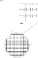
- FIG. 3 is a plan view illustrating the arrangement of shots on the wafer W.
- the wafer W includes a plurality of shots S on the surface thereof, and a plurality of alignment marks AMW is formed in each shot S.
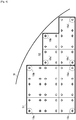
- FIG. 4 is a diagram illustrating the alignment of peripheral shots on the wafer.
- the shot S present on the wafer W is basically rectangular as shown in a shot S1 in FIG. 4 .
- the entire one shot does not fall within the wafer W in the periphery of the wafer W, and thus, the shot S2 has a different shape from that of the shot S1.
- the positions of the alignment scopes 19 are the regions 19a' to 19d' with respect to the peripheral shot S2 that is present in the periphery of the wafer W as described above, and the detail of which will be described below.
- the controller 7 may control the operation, adjustment, and the like of the components of the imprint apparatus 1.
- the controller 7 is constituted by a computer or the like and is connected to the components of the imprint apparatus 1 through a line so as to execute control of the components by a program or the like.
- the controller 7 of the present embodiment controls at least the operation of the alignment detection system 6 and the wafer stage 4. Note that the controller 7 may be integrated with the rest of the imprint apparatus 1 (provided in a shared housing) or may be provided separately from the rest of the imprint apparatus 1 (provided in a separate housing).
- the imprint apparatus 1 includes a surface plate (not shown) for forming a reference plane on which the wafer stage 4 is placed, a bridge surface plate 15 that fixes the mold holding mechanism 3, and a column that extends from the surface plate and supports the bridge surface plate 15 via a vibration isolator that isolates vibration from a floor.
- the imprint apparatus 1 may include a mold conveyance mechanism that conveys into/out the mold M between the exterior of the imprint apparatus 1 and the mold holding mechanism 3 and a substrate conveyance mechanism that conveys into/out the wafer W between the exterior of the imprint apparatus 1 and the wafer stage 4, and the like, and none of which is shown.
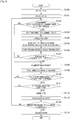
- FIG. 5 is a flowchart illustrating the sequence of operations of a series of imprint processing performed by the imprint apparatus 1.
- the controller 7 causes the mold conveyance mechanism to convey the mold M to the mold chuck 13 and causes the mold chuck 13 to hold the mold M after positioning (step S100).
- the controller 7 causes the alignment stage mechanism 20 to move the alignment scope 19.
- the controller 7 performs control to operate the alignment scope 19 such that the detection position of the alignment scope 19 is positioned at the alignment marks AMW which are present at the four corners (the regions 19a to 19d) of the shot as shown in FIG. 2C (the shot S1 as shown in FIG.
- the controller 7 causes the substrate conveyance mechanism to convey the wafer W to the wafer chuck 17 and then causes the wafer chuck 17 to hold the wafer W (step S101). It should be noted that at least one layer pattern has already been formed together with the alignment marks AMW on each shot on the wafer W.
- the controller 7 causes the alignment detection system 6 to measure the relative position between the alignment marks AMM on the mold M and the alignment marks AMW on the wafer W. At this time, the controller 7 determines whether or not the alignment scope 19 is positioned at the detection position of each alignment mark AMM on the mold M, i.e., at the position corresponding to the regions 19a to 19d (step S102). In normal measurement for measuring the shot S1 as shown in FIG. 4 upon installation of the mold M, the position of the alignment scope 19 is matched with the regions 19a to 19d as it is.
- step S102 when the controller 7 determines in step S102 that the position of the alignment scope 19 is located on the regions 19a to 19d (YES), the process shifts to the following step S104 because the controller 7 is capable of being put into alignment measurement without changing the position of the alignment scope 19.
- step S104 when the position of the alignment scope 19 remains the same upon measurement of the peripheral shot S2 as shown in FIG. 4 , there is no alignment mark AMW corresponding to two regions 19a and 19b on the shot S2, and thus, the positions of the two regions 19a and 19b cannot be measured.
- step S103 when the controller 7 determines in step S102 that the position of the alignment scope 19 is not located on the regions 19a to 19d (NO), the controller 7 causes the alignment stage mechanism 20 to start movement of the alignment scope 19 (step S103).
- the controller 7 performs control to select the alignment marks AMW, which are present at positions where the distance between the alignment marks AMW can be set as wide as possible, from among a plurality of alignment marks AMW present within the peripheral shot S2. For example, in the case of the peripheral shot S2 shown in FIG. 4 , four alignment marks AMW corresponding to the regions 19a' to 19d' are the preferable alignment marks.
- step S104 application step.
- the controller 7 causes the stage drive mechanism 18 to move the wafer W so as to make a shot to be processed this time position at the application position of the dispenser 5 and causes the dispenser 5 to apply the resin R to the wafer W (step S104: application step).
- the controller 7 performs control to move the alignment scope 19 concurrently with the movement of the wafer W to the application position.
- the controller 7 causes the stage drive mechanism 18 to move the wafer W such that the shot is positioned at a position where the wafer W is pressed against the mold M (step S105).
- the controller 7 cannot immediately perform alignment processing because there is a possibility at this stage that the alignment scope 19 that has started to move in step S103 is still in the middle of movement.
- the pressing operation of pressing the mold M against the resin R on the wafer W in the following mold-pressing step is not necessarily performed after alignment processing is strictly performed, that is, after the alignment marks AMM on the mold M are strictly matched with the alignment marks AMW on the wafer W.
- the controller 7 can performs strict alignment processing during the pressing operation so as to deform (correct) the shape of the resin R at that time as appropriate.
- the controller 7 causes the stage drive mechanism 18 to move the wafer W with reference to a shot position obtained when alignment processing is performed for a shot previously processed.
- the controller 7 performs control to start a pressing operation (step S106: mold-pressing step).
- the controller 7 may perform control to start the pressing operation at a position where the wafer W is shifted by the size of one shot on the basis of the alignment of the shot S1.
- the pressing operation is performed by the controller 7 by causing the mold drive mechanism 14 to lift down the mold M toward the resin R on the wafer W.
- the controller 7 may perform the pressing operation for pressing the mold M against the resin R by lifting up the wafer W instead of driving the mold M.
- the controller 7 may control a pressing load by using a load sensor incorporated in the mold drive mechanism 14.
- step S107 when the alignment scope 19 has been moved in step S103, the controller 7 determines whether or not the movement of the alignment scope 19 is completed (step S107).
- the controller 7 determines that the movement of the alignment scope 19 is not completed (NO)
- the controller 7 performs control to continue determination processing until the movement of the alignment scope 19 is completed.
- the controller 7 determines that the movement of the alignment scope 19 is completed (YES) and when the movement of the alignment scope 19 is absent in step S103
- the controller 7 causes the alignment scope 19 to perform alignment measurement in a dye-by-dye alignment method (step S108).
- the controller 7 causes the alignment scope 19 to capture images of the alignment marks AMM on the mold M and the alignment marks AMW on the wafer W and causes an image processing apparatus (not shown) to measure the relative position between the alignment marks AMM and AMW. Then, the controller 7 computes the difference (coordinate component, rotation component, magnification component, trapezoidal component, and the like) of shot shapes between the mold M and the wafer W based on the results of detection at four positions corresponding to the regions 19a to 19d (or the regions 19a' to 19d').
- the controller 7 causes the magnification correction mechanism 16 to correct the shape of the mold M so as to match the shape of the pattern section formed on the mold M with the shape of the shot on the wafer W as appropriate concurrently with positioning of the wafer W relative to the mold M (step S109).
- the controller 7 then performs shape difference tolerance determination because a correction error may occur due to driving error in driving the magnification correction mechanism 16 (step S110).
- the controller 7 determines that the shape difference is equal to or greater than a tolerance level (NO)
- the process returns to step S108, and the controller 7 causes the alignment scope 19 to perform alignment measurement again and causes the magnification correction mechanism 16 to correct the shape of the mold M until the shape difference is equal to or less than a predetermined tolerance level.
- step S110 determines whether or not the shape difference is equal to or less than a tolerance level (YES)
- step S111 determines whether or not the pressing operation is completed (whether or not the filling of the resin R in the mold M is completed)
- step S111 determines whether or not the filling of the resin R in the mold M is completed.
- the process returns to step S108 again and the controller 7 causes the alignment scope 19 to perform alignment measurement.
- step S111 the controller 7 causes the light irradiation unit 2 to irradiate the resin R on the wafer W with the ultraviolet light 10 via the mold M to thereby cure the resin R (step S112: curing step). After the resin R is cured, the controller 7 causes the mold drive mechanism 14 to raise the mold M to thereby release the mold M from the cured resin R (step S113: mold-releasing step).
- the controller 7 determines whether or not imprint processing (pattern-forming step) has been completed for all the shots on the wafer W (step S114).
- the controller 7 determines that there is still a shot not subjected to imprint processing (NO)
- the process returns to step S102 and the controller 7 performs control to repeat imprint processing for the next shot.
- the controller 7 determines that imprint processing has been completed for all the shots on the wafer W (YES in step S114)
- the controller 7 causes the substrate conveyance mechanism to collect the wafer W from the wafer chuck 17 (step S115), and all the processing ends.
- the controller 7 causes the alignment scope 19 to move to a position at which a detectable alignment mark is present.
- the imprint apparatus 1 may perform accurate alignment processing even when a shot to be processed is a peripheral shot.
- the mold-pressing step pressing operation
- the controller 7 simultaneously performs control to start the application step and the next mold-pressing step immediately after the start of the movement of the alignment scope 19.
- the imprint apparatus 1 can increase its throughput.
- the controller 7 causes the stage drive mechanism 18 to move the wafer W with reference to a shot position obtained when alignment processing is performed for a shot previously processed.
- the alignment scope 19 can set the position of the wafer W to a position near the exact location even when the movement destination position is not accurately recognized.
- the imprint apparatus 1 can also perform the position settings in a short period of time, resulting in a further increase in throughput.
- an imprint method that is advantageous for improving throughput may be provided.
- the controller 7 performs control to start the pressing operation for the next shot with reference to the shot subjected to the most-recent imprint processing.
- the controller 7 performs control to move two alignment scopes 19 corresponding to the other two regions 19a' and 19b'.
- the alignment scopes 19 corresponding to the regions 19a' and 19b' cannot be used, whereas the alignment scopes 19 corresponding to the regions 19c' and 19d' can be used.
- the controller 7 is not limited to start the pressing operation with reference to all the positions on the shot subjected to the most-recent imprint processing but may also perform alignment processing using the non-move alignment scope 19 and then start the pressing operation. Then, after the movement of all the alignment scopes 19 is completed, the controller 7 may perform dye-by-dye alignment in step S108.
- the controller 7 determines whether or not the movement of the alignment scope 19 is necessary prior to the application step (step S104) of application the resin R in the imprint cycle, and performs the movement of the alignment scope 19 as appropriate.
- the controller 7 may also determine whether or not the movement of the alignment scope 19 is necessary based on the shape of the next shot after the shape difference becomes equal to or less than the tolerance level and the filling is completed.
- the controller 7 performs the movement of the alignment scope 19 ahead of its schedule so that the movement of the alignment scope 19 is completed at an earlier timing, whereby the total processing time required for performing imprint processing for all the shots on the wafer W can further be reduced.
- a method for manufacturing a device may include a step of forming a pattern on a substrate (wafer, glass plate, film-like substrate, or the like) using the imprint apparatus described above. Furthermore, the manufacturing method may include a step of etching the substrate on which a pattern has been formed. When other article such as a patterned medium (storage medium), an optical element, or the like is manufactured, the manufacturing method may include other step of processing the substrate on which a pattern has been formed instead of the etching step.
- the article manufacturing method of the present embodiment has an advantage, as compared with a conventional article manufacturing method, in at least one of performance, quality, productivity and production cost of an article.
Description
- The present invention relates to an imprint method and an imprint apparatus, and an article manufacturing method using the same.
- As the demand for microfabrication of semiconductor devices or MEMS increases, not only a conventional photolithography technology but also a microfabrication technology in which an uncured resin on a substrate (wafer) is molded by a mold to thereby form a resin pattern on the substrate have been receiving attention. This technology is also referred to as an "imprint technology", by which a fine structure with dimensions of a few nanometers can be formed on a substrate. One example of imprint technologies includes a photo-curing method. An imprint apparatus employing the photo-curing method first applies an ultraviolet curable resin (imprint material, photocurable resin) to a shot region (imprint region) on a substrate. Next, the resin (uncured resin) is molded by a mold. After the ultraviolet curable resin is irradiated with ultraviolet light for curing, the cured resin is released from the mold, whereby a resin pattern is formed on a substrate. In particular, the imprint apparatus disclosed in
Patent Literature 1 causes an alignment detection system to detect a shot that is present on the peripheral region of a substrate, on which no alignment mark is missing from among the alignment marks on shots, in advance when a pattern is formed on the shots (peripheral shots) present on the peripheral region of the substrate. - Patent Literature 1: Japanese Patent Laid-Open No.
2007-281072 - Here, the shape of the peripheral shot is different for each peripheral shot. Thus, the position of an alignment mark to be detected by an alignment detection system also differs for each peripheral shot. In the imprint apparatus disclosed in
Patent Literature 1, the operation of performing alignment measurement and bringing an imprint material into contact with a mold is started after movement (alignment) of the alignment detection system to the detection position. Therefore, the alignment detection system needs to move for the detection of an alignment mark, and its movement time results in an adverse effect on throughput. - Patent Literature 2:
EP 1 669 802 A2 - Accordingly, the present invention provides an imprint method that is advantageous for improving throughput.
- According to an aspect of the present invention, an imprint method as defined in
claims claim 7 is provided. The other claims relate to further developments. - According to the present invention, an imprint method that is advantageous for improving throughput may be provided.
- Further features of the present invention will become apparent from the following description of exemplary embodiments with reference to the attached drawings.
-
-
FIG. 1 is a diagram illustrating the configuration of an imprint apparatus according to one embodiment of the present invention. -
FIG. 2A is a diagram illustrating the arrangement of an alignment scope. -
FIG. 2B is an enlarged view illustrating an alignment mark as viewed from the ultraviolet light incident side. -
FIG. 2C is a diagram illustrating a plurality of alignment marks as viewed from the ultraviolet light incident side. -
FIG. 3 is a diagram illustrating alignment of peripheral shots on a wafer. -
FIG. 4 is a diagram illustrating the arrangement of shots on a wafer. -
FIG. 5 is a flowchart illustrating the sequence of operations during imprint processing. - Hereinafter, preferred embodiments of the present invention will be described with reference to the drawings.
- Firstly, a description will be given of the configuration of an imprint apparatus according to one embodiment of the present invention.
FIG. 1 is a schematic diagram illustrating the configuration of animprint apparatus 1 of the present embodiment. Theimprint apparatus 1 is an apparatus that molds an uncured resin (imprint material) on a wafer (on a substrate), i.e., a substrate to be treated, using a mold to thereby form a resin pattern on the wafer, which is used in the manufacture of devices such as semiconductor devices and the like as articles. Here, the imprint apparatus of the present embodiment is an imprint apparatus employing a photo-curing method for curing a resin by the irradiation of ultraviolet light. Theimprint apparatus 1 sequentially forms a pattern on a plurality of shots (pattern-forming regions) present on a wafer by repeating an imprint cycle. Here, the imprint cycle refers to a cycle for forming a pattern on one shot on a wafer by curing a resin while a mold is being pressed against the resin on the wafer (while a mold is brought into contact with the resin on the wafer). In the following drawings, a description will be given where the Z axis is aligned parallel to the optical axis of an irradiation system that irradiates a resin on a wafer with ultraviolet light, and mutually orthogonal axes X and Y are aligned in a plane perpendicular to the Z axis. Theimprint apparatus 1 includes alight irradiation unit 2, amold holding mechanism 3, awafer stage 4, adispenser 5, analignment detection system 6, and acontroller 7. - The
light irradiation unit 2 irradiates a resin R with theultraviolet light 10 via a mold M to thereby cure the resin R. The resin R in the present embodiment is an ultraviolet curable resin. Thelight irradiation unit 2 includes alight source unit 8 and anoptical system 9. Thelight source unit 8 includes a light source (not shown) such as a halogen lamp for emitting the ultraviolet light 10 (e.g., i-rays, g-rays) and an elliptical mirror (not shown) for collecting light emitted from the light source. Theoptical system 9 includes a lens and an aperture (not shown) used for irradiating the resin R on a shot with theultraviolet light 10, and ahalf mirror 11. The aperture is used for field angle control and outer peripheral light-shielding control. With the aid of the field angle control, only a target shot can be irradiated with theultraviolet light 10. With the aid of the outer peripheral light-shielding control, theultraviolet light 10 can be limited so as not to exceed the external shape of a wafer W. Theoptical system 9 may also include an optical integrator for uniformly illuminating the mold M. Theultraviolet light 10 of which the illumination range has been defined by the aperture is incident on the resin R on the wafer W via the mold M. Furthermore, in the present embodiment, theimprint apparatus 1 includes anobservation scope 12 that observes the entire shot via thehalf mirror 11. Theobservation scope 12 is used for confirming the state of imprint processing (a pressing operation and progress state of filling). - The outer peripheral shape of the mold M is a polygon (preferably, rectangular or square) and the mold M includes a pattern section (e.g., the concave and convex pattern of a circuit pattern or the like to be transferred) which is three-dimensionally formed on the surface facing the wafer W. In order to pass through the
ultraviolet light 10 for curing the resin R, the mold M is formed of any material which is transparent to wavelengths of theultraviolet light 10, such as quartz. - The
mold holding mechanism 3 includes amold chuck 13 that holds the mold M and amold drive mechanism 14 that moves the mold chuck 13 (the mold M). Themold drive mechanism 14 is supported on thebridge surface plate 15. Themold drive mechanism 14 includes a positioning mechanism that controls the position of the mold M in the directions of six axes and a mechanism that presses the mold M against the resin R on the wafer W and releases the mold M from the cured resin R. Here, the six axes refer to the X axis, the Y axis, the Z axis, and the rotation direction of each axis in the XYZ coordinate system where the support plane of the mold chuck 13 (plane for supporting the wafer W) is aligned to the XY-plane and the direction orthogonal to the XY-plane is aligned to the Z axis. Furthermore, themold holding mechanism 3 includes a magnification correction mechanism (shape correction mechanism) 16 that is installed on themold chuck 13. Themagnification correction mechanism 16 corrects the shape of the mold M by applying pressure to the mold M from the outer peripheral direction using, for example, a cylinder that operates with a fluid such as air or oil. Also, themagnification correction mechanism 16 corrects the shape of the mold M by controlling the temperature of the mold M using a temperature controller that controls the temperature of the mold M. The wafer W is deformed (in general, expanded or contracted) by carrying out the process such as heat treatment. Accordingly, themagnification correction mechanism 16 corrects the shape of the mold M depending on the deformation of the wafer W described above such that an overlay error falls within an allowable range. - The wafer W is, for example, a single crystal silicon substrate, an SOI (Silicon on Insulator) substrate, or a glass substrate. The pattern (pattern-including layer) of the resin R is formed on a plurality of shots on the wafer W by a pattern section (the pattern (hereinafter referred to as a 'wafer W-side pattern') has already been formed in the previous step before the wafer W is conveyed into the imprint apparatus 1).
- The wafer stage (substrate holding unit) 4 includes a
wafer chuck 17 that holds the wafer W by sucking it by vacuum suction and astage drive mechanism 18 that moves the wafer chuck 17 (the wafer W). As in themold drive mechanism 14, thestage drive mechanism 18 includes a positioning mechanism that controls the position of the wafer W by controlling the position of thewafer chuck 17 in the directions of six axes. - The
dispenser 5 applies the resin R to a shot on the wafer W. Thedispenser 5 includes a tank that contains therein the resin R, a nozzle that discharges the resin R supplied from the tank via a supply passage to the wafer W, a valve provided on the supply passage, and a supply amount controller, all of which are not shown. In general, the supply amount controller is configured to control the valve such that the resin R is applied to one shot in a single discharge operation for discharging the resin R to thereby adjust the supply amount of the resin R to the wafer W. - The
alignment detection system 6 includes a plurality of (in this case, four) alignment scopes (detectors) 19 and analignment stage mechanism 20. Thealignment scope 19 detects an alignment mark AMM formed on the mold M and an alignment mark AMW formed on the wafer W via the mold M so as to perform positioning between the mold M and the wafer W. Thealignment stage mechanism 20 is mounted on thebridge surface plate 15 and can move a plurality of thealignment scopes 19 independently so as to change the detection position to be detected by eachalignment scope 19. -
FIGs. 2A to 2C are diagrams illustrating the arrangement of thealignment scope 19, and a mold-side alignment mark AMM formed on the mold M and a wafer-side alignment mark AMW formed on the wafer W. In particular,FIG. 2A is a schematic cross-sectional view illustrating the arrangement of thealignment scopes 19, the mold M, the resin R, and the wafer W.FIG. 2B is an enlarged view illustrating the alignment marks AMM and AMW as viewed from the ultraviolet light incident side. The alignment mark AMM and the alignment mark AMW are arranged so as not to overlap with each other as viewed from the ultraviolet light incident side to the mold M in the state shown inFIG. 2A . Furthermore,FIG. 2C is a schematic plan view illustrating the arrangement of a plurality of alignment marks AMM and AMW as viewed from the ultraviolet light incident side to the mold M. In particular, theregions 19a to 19d at the four corners of the mold M are regions that are the positions (detection positions) to be (specifically) detected by thealignment scopes 19. On the other hand,FIG. 3 is a plan view illustrating the arrangement of shots on the wafer W. The wafer W includes a plurality of shots S on the surface thereof, and a plurality of alignment marks AMW is formed in each shot S. -
FIG. 4 is a diagram illustrating the alignment of peripheral shots on the wafer. The shot S present on the wafer W is basically rectangular as shown in a shot S1 inFIG. 4 . However, the entire one shot does not fall within the wafer W in the periphery of the wafer W, and thus, the shot S2 has a different shape from that of the shot S1. Accordingly, in the present embodiment, the positions of thealignment scopes 19 are theregions 19a' to 19d' with respect to the peripheral shot S2 that is present in the periphery of the wafer W as described above, and the detail of which will be described below. - The
controller 7 may control the operation, adjustment, and the like of the components of theimprint apparatus 1. Thecontroller 7 is constituted by a computer or the like and is connected to the components of theimprint apparatus 1 through a line so as to execute control of the components by a program or the like. Thecontroller 7 of the present embodiment controls at least the operation of thealignment detection system 6 and thewafer stage 4. Note that thecontroller 7 may be integrated with the rest of the imprint apparatus 1 (provided in a shared housing) or may be provided separately from the rest of the imprint apparatus 1 (provided in a separate housing). - Furthermore, the
imprint apparatus 1 includes a surface plate (not shown) for forming a reference plane on which thewafer stage 4 is placed, abridge surface plate 15 that fixes themold holding mechanism 3, and a column that extends from the surface plate and supports thebridge surface plate 15 via a vibration isolator that isolates vibration from a floor. Furthermore, theimprint apparatus 1 may include a mold conveyance mechanism that conveys into/out the mold M between the exterior of theimprint apparatus 1 and themold holding mechanism 3 and a substrate conveyance mechanism that conveys into/out the wafer W between the exterior of theimprint apparatus 1 and thewafer stage 4, and the like, and none of which is shown. - Next, a description will be given of an imprint method performed by the
imprint apparatus 1.FIG. 5 is a flowchart illustrating the sequence of operations of a series of imprint processing performed by theimprint apparatus 1. Firstly, thecontroller 7 causes the mold conveyance mechanism to convey the mold M to themold chuck 13 and causes themold chuck 13 to hold the mold M after positioning (step S100). Here, after installation of the mold M, thecontroller 7 causes thealignment stage mechanism 20 to move thealignment scope 19. In particular, in the present embodiment, thecontroller 7 performs control to operate thealignment scope 19 such that the detection position of thealignment scope 19 is positioned at the alignment marks AMW which are present at the four corners (theregions 19a to 19d) of the shot as shown inFIG. 2C (the shot S1 as shown inFIG. 4 ). Next, thecontroller 7 causes the substrate conveyance mechanism to convey the wafer W to thewafer chuck 17 and then causes thewafer chuck 17 to hold the wafer W (step S101). It should be noted that at least one layer pattern has already been formed together with the alignment marks AMW on each shot on the wafer W. - Next, the
controller 7 causes thealignment detection system 6 to measure the relative position between the alignment marks AMM on the mold M and the alignment marks AMW on the wafer W. At this time, thecontroller 7 determines whether or not thealignment scope 19 is positioned at the detection position of each alignment mark AMM on the mold M, i.e., at the position corresponding to theregions 19a to 19d (step S102). In normal measurement for measuring the shot S1 as shown inFIG. 4 upon installation of the mold M, the position of thealignment scope 19 is matched with theregions 19a to 19d as it is. Thus, when thecontroller 7 determines in step S102 that the position of thealignment scope 19 is located on theregions 19a to 19d (YES), the process shifts to the following step S104 because thecontroller 7 is capable of being put into alignment measurement without changing the position of thealignment scope 19. In contrast, when the position of thealignment scope 19 remains the same upon measurement of the peripheral shot S2 as shown inFIG. 4 , there is no alignment mark AMW corresponding to tworegions regions controller 7 determines in step S102 that the position of thealignment scope 19 is not located on theregions 19a to 19d (NO), thecontroller 7 causes thealignment stage mechanism 20 to start movement of the alignment scope 19 (step S103). At this time, the detection position of the alignment mark AMW can be changed. Thus, it is preferable that thecontroller 7 performs control to select the alignment marks AMW, which are present at positions where the distance between the alignment marks AMW can be set as wide as possible, from among a plurality of alignment marks AMW present within the peripheral shot S2. For example, in the case of the peripheral shot S2 shown inFIG. 4 , four alignment marks AMW corresponding to theregions 19a' to 19d' are the preferable alignment marks. - Next, the
controller 7 causes thestage drive mechanism 18 to move the wafer W so as to make a shot to be processed this time position at the application position of thedispenser 5 and causes thedispenser 5 to apply the resin R to the wafer W (step S104: application step). Here, when thealignment scope 19 has been moved in step S103, it is preferable that thecontroller 7 performs control to move thealignment scope 19 concurrently with the movement of the wafer W to the application position. - Next, the
controller 7 causes thestage drive mechanism 18 to move the wafer W such that the shot is positioned at a position where the wafer W is pressed against the mold M (step S105). Here, when thealignment scope 19 has been moved in step S103, thecontroller 7 cannot immediately perform alignment processing because there is a possibility at this stage that thealignment scope 19 that has started to move in step S103 is still in the middle of movement. However, the pressing operation of pressing the mold M against the resin R on the wafer W in the following mold-pressing step is not necessarily performed after alignment processing is strictly performed, that is, after the alignment marks AMM on the mold M are strictly matched with the alignment marks AMW on the wafer W. This is because, if the resin R is not yet cured even during the pressing operation of pressing the mold M against the resin R on the wafer W, thecontroller 7 can performs strict alignment processing during the pressing operation so as to deform (correct) the shape of the resin R at that time as appropriate. In the present embodiment, thecontroller 7 causes thestage drive mechanism 18 to move the wafer W with reference to a shot position obtained when alignment processing is performed for a shot previously processed. Next, thecontroller 7 performs control to start a pressing operation (step S106: mold-pressing step). More specifically, when the shot S1 subjected to imprint processing is present prior to imprint processing for the current shot S2, thecontroller 7 may perform control to start the pressing operation at a position where the wafer W is shifted by the size of one shot on the basis of the alignment of the shot S1. Here, the pressing operation is performed by thecontroller 7 by causing themold drive mechanism 14 to lift down the mold M toward the resin R on the wafer W. Note that thecontroller 7 may perform the pressing operation for pressing the mold M against the resin R by lifting up the wafer W instead of driving the mold M. Also, thecontroller 7 may control a pressing load by using a load sensor incorporated in themold drive mechanism 14. - Next, when the
alignment scope 19 has been moved in step S103, thecontroller 7 determines whether or not the movement of thealignment scope 19 is completed (step S107). Here, when thecontroller 7 determines that the movement of thealignment scope 19 is not completed (NO), thecontroller 7 performs control to continue determination processing until the movement of thealignment scope 19 is completed. On the other hand, when thecontroller 7 determines that the movement of thealignment scope 19 is completed (YES) and when the movement of thealignment scope 19 is absent in step S103, thecontroller 7 causes thealignment scope 19 to perform alignment measurement in a dye-by-dye alignment method (step S108). Here, thecontroller 7 causes thealignment scope 19 to capture images of the alignment marks AMM on the mold M and the alignment marks AMW on the wafer W and causes an image processing apparatus (not shown) to measure the relative position between the alignment marks AMM and AMW. Then, thecontroller 7 computes the difference (coordinate component, rotation component, magnification component, trapezoidal component, and the like) of shot shapes between the mold M and the wafer W based on the results of detection at four positions corresponding to theregions 19a to 19d (or theregions 19a' to 19d'). - Next, the
controller 7 causes themagnification correction mechanism 16 to correct the shape of the mold M so as to match the shape of the pattern section formed on the mold M with the shape of the shot on the wafer W as appropriate concurrently with positioning of the wafer W relative to the mold M (step S109). Thecontroller 7 then performs shape difference tolerance determination because a correction error may occur due to driving error in driving the magnification correction mechanism 16 (step S110). Here, when thecontroller 7 determines that the shape difference is equal to or greater than a tolerance level (NO), the process returns to step S108, and thecontroller 7 causes thealignment scope 19 to perform alignment measurement again and causes themagnification correction mechanism 16 to correct the shape of the mold M until the shape difference is equal to or less than a predetermined tolerance level. On the other hand, when thecontroller 7 determines in step S110 that the shape difference is equal to or less than a tolerance level (YES), thecontroller 7 determines whether or not the pressing operation is completed (whether or not the filling of the resin R in the mold M is completed) (step S111). Here, when thecontroller 7 determines that the filling of the resin R in the mold M is not completed (NO), the process returns to step S108 again and thecontroller 7 causes thealignment scope 19 to perform alignment measurement. - Next, upon completion of the filling of the resin R in the mold M (YES in step S111), the
controller 7 causes thelight irradiation unit 2 to irradiate the resin R on the wafer W with theultraviolet light 10 via the mold M to thereby cure the resin R (step S112: curing step). After the resin R is cured, thecontroller 7 causes themold drive mechanism 14 to raise the mold M to thereby release the mold M from the cured resin R (step S113: mold-releasing step). - Next, the
controller 7 determines whether or not imprint processing (pattern-forming step) has been completed for all the shots on the wafer W (step S114). Here, when thecontroller 7 determines that there is still a shot not subjected to imprint processing (NO), the process returns to step S102 and thecontroller 7 performs control to repeat imprint processing for the next shot. On the other hand, when thecontroller 7 determines that imprint processing has been completed for all the shots on the wafer W (YES in step S114), thecontroller 7 causes the substrate conveyance mechanism to collect the wafer W from the wafer chuck 17 (step S115), and all the processing ends. - As described above, when a shot to be processed is a peripheral shot and alignment processing is performed for the peripheral shot, the
controller 7 causes thealignment scope 19 to move to a position at which a detectable alignment mark is present. In this manner, theimprint apparatus 1 may perform accurate alignment processing even when a shot to be processed is a peripheral shot. However, if the mold-pressing step (pressing operation) is performed after waiting for the completion of the movement of thealignment scope 19, the time required for the entire imprint processing is prolonged, resulting in a decrease in throughput. Thus, in the present embodiment, thecontroller 7 simultaneously performs control to start the application step and the next mold-pressing step immediately after the start of the movement of thealignment scope 19. Thus, at least a part of the movement time of thealignment scope 19 overlaps the pressing time (the filling time of the resin R), that is, is hidden within the pressing time, whereby the time required for the entire imprint processing can be shortened. In this manner, theimprint apparatus 1 can increase its throughput. Furthermore, in the present embodiment, when a shot is moved to a pressing position after the application step, thecontroller 7 causes thestage drive mechanism 18 to move the wafer W with reference to a shot position obtained when alignment processing is performed for a shot previously processed. In this manner, thealignment scope 19 can set the position of the wafer W to a position near the exact location even when the movement destination position is not accurately recognized. Thus, theimprint apparatus 1 can also perform the position settings in a short period of time, resulting in a further increase in throughput. - As described above, according to the present embodiment, an imprint method that is advantageous for improving throughput may be provided.
- In the above embodiment, the
controller 7 performs control to start the pressing operation for the next shot with reference to the shot subjected to the most-recent imprint processing. Here, For example, when imprint processing is performed for the shot S2 subsequent to the shot S1 as shown in the example inFIG. 4 , no change is made on tworegions 19c' and 19d'. In other words, thecontroller 7 performs control to move twoalignment scopes 19 corresponding to the other tworegions 19a' and 19b'. Thus, during that time, thealignment scopes 19 corresponding to theregions 19a' and 19b' cannot be used, whereas thealignment scopes 19 corresponding to theregions 19c' and 19d' can be used. As described above, thecontroller 7 is not limited to start the pressing operation with reference to all the positions on the shot subjected to the most-recent imprint processing but may also perform alignment processing using thenon-move alignment scope 19 and then start the pressing operation. Then, after the movement of all thealignment scopes 19 is completed, thecontroller 7 may perform dye-by-dye alignment in step S108. - Furthermore, in the embodiment, the
controller 7 determines whether or not the movement of thealignment scope 19 is necessary prior to the application step (step S104) of application the resin R in the imprint cycle, and performs the movement of thealignment scope 19 as appropriate. However, thecontroller 7 may also determine whether or not the movement of thealignment scope 19 is necessary based on the shape of the next shot after the shape difference becomes equal to or less than the tolerance level and the filling is completed. Thecontroller 7 performs the movement of thealignment scope 19 ahead of its schedule so that the movement of thealignment scope 19 is completed at an earlier timing, whereby the total processing time required for performing imprint processing for all the shots on the wafer W can further be reduced. - A method for manufacturing a device (semiconductor integrated circuit element, liquid display element, or the like) as an article may include a step of forming a pattern on a substrate (wafer, glass plate, film-like substrate, or the like) using the imprint apparatus described above. Furthermore, the manufacturing method may include a step of etching the substrate on which a pattern has been formed. When other article such as a patterned medium (storage medium), an optical element, or the like is manufactured, the manufacturing method may include other step of processing the substrate on which a pattern has been formed instead of the etching step. The article manufacturing method of the present embodiment has an advantage, as compared with a conventional article manufacturing method, in at least one of performance, quality, productivity and production cost of an article.
- While the present invention has been described with reference to exemplary embodiments, it is to be understood that the invention is not limited to the disclosed exemplary embodiments. The scope of the following claims is to be accorded the broadest interpretation so as to encompass all such modifications and equivalent structures and functions.
- This application claims the benefit of Japanese Patent Application No.
2012-053991 filed on March 12, 2012 2013-042700 filed on March 5, 2013
Claims (11)
- An imprint method for bringing an imprint material on a substrate into contact with a mold to form a pattern of the imprint material, the imprint method comprising:changing a position of a detector that detects an alignment mark formed on a shot region on the substrate (S103, S107);contacting the mold with the imprint material supplied on the shot region on the substrate (S106, S111); anddetecting the alignment mark using the detector after completion of the changing of the position of the detector (S108),characterized in thatthe changing of the position of the detector is started (S103) before the contacting the mold with the imprint material (S106), andthe contacting is started (S106) prior to completion (S107) of the changing of the position of the detector.
- The imprint method according to claim 1, wherein the contacting is started based on the result of detection obtained by detecting an alignment mark with respect to another shot region at which the pattern is transferred to the imprint material.
- The imprint method according to claim 1, wherein the imprint method repeatedly transfers a pattern formed on the mold to a plurality of shot regions formed on the substrate, and the changing of the position of the detector is to change the position of the detector from the position of a shot region to which the pattern formed on the mold has been transferred to the position of the next shot region on the substrate to which the pattern is to be transferred.
- The imprint method according to claim 1, wherein, when the detector is provided in plural and there are the detector of which the position is changed in the changing of the position of the detector and the detector of which the position is not changed, the detector of which the position is not changed starts the contacting of the mold by detecting the alignment mark, and the detector of which the position is changed detects the alignment mark after completion of the change in the position of the detector of which the position is changed.
- The imprint method according to claim 1, further comprising:curing the uncured imprint material on the shot region after completion of the contacting;releasing the mold from the cured imprint material; anddetecting an alignment mark formed on the shot region to be next processed prior to the curing or the releasing after completion of at least one of matching the shape of the pattern formed on the mold with the shape of the shot region and aligning the mold with the substrate.
- An imprint method for bringing an imprint material on a substrate into contact with a mold to form a pattern of the imprint material, the imprint method comprising:supplying the imprint material on the substrate (S104);changing the position of a detector that detects an alignment mark formed on a shot region on the substrate (S103, S107);contacting the mold with the imprint material supplied on the shot region on the substrate (S106, S111); anddetecting the alignment mark using the detector after completion of the changing of the position of the detector (S108),characterized in that supplying the imprint material (S104) is performed during the changing of the position of the detector (S103, S107).
- An imprint apparatus configured to bring an imprint material (R) on a substrate (W) into contact with a mold (M) to form a pattern of the imprint material, the imprint apparatus comprising:a detector (19) configured to detect an alignment mark (AMM, AMW), among a plurality of alignment marks formed on a shot region on the substrate, to allow the detection position of the alignment mark to be changed; andcharacterized by further comprising: a controller (7) configured to start changing the position of the detector before contacting the mold and the imprint material and to start bringing the mold into contact with the imprint material supplied on the shot region on the substrate prior to the change in the position of the detector being completed.
- An article manufacturing method comprising:forming an imprint material pattern on a substrate using the imprint method according to claim 1; andprocessing the substrate on which the pattern has been formed in the forming.
- An article manufacturing method comprising:forming an imprint material pattern on a substrate using the imprint method according to claim 6; andprocessing the substrate on which the pattern has been formed in the forming.
- An article manufacturing method comprising:forming an imprint material pattern on a substrate using the imprint apparatus according to claim 7; andprocessing the substrate on which the pattern has been formed in the forming.
- An imprint apparatus configured to bring an imprint material (R) on a substrate (W) into contact with a mold (M) to form a pattern of the imprint material, the imprint apparatus comprising:a detector (19) configured to detect an alignment mark (AMM, AMW), among a plurality of alignment marks formed on a shot region on the substrate, to allow the detection position of the alignment mark to be changed;characterized by further comprising:
a controller (7) configured to supply the imprint material on the shot region on the substrate during the changing of the position of the detector.
Applications Claiming Priority (3)
| Application Number | Priority Date | Filing Date | Title |
|---|---|---|---|
| JP2012053991 | 2012-03-12 | ||
| JP2013042700A JP6029495B2 (en) | 2012-03-12 | 2013-03-05 | Imprint method, imprint apparatus, and article manufacturing method using the same |
| PCT/JP2013/001446 WO2013136733A1 (en) | 2012-03-12 | 2013-03-07 | Imprint method, imprint apparatus, and article manufacturing method |
Publications (3)
| Publication Number | Publication Date |
|---|---|
| EP2826059A1 EP2826059A1 (en) | 2015-01-21 |
| EP2826059A4 EP2826059A4 (en) | 2015-11-18 |
| EP2826059B1 true EP2826059B1 (en) | 2019-10-09 |
Family
ID=49160666
Family Applications (1)
| Application Number | Title | Priority Date | Filing Date |
|---|---|---|---|
| EP13760289.2A Active EP2826059B1 (en) | 2012-03-12 | 2013-03-07 | Imprint method, imprint apparatus, and article manufacturing method |
Country Status (6)
| Country | Link |
|---|---|
| US (1) | US9703190B2 (en) |
| EP (1) | EP2826059B1 (en) |
| JP (1) | JP6029495B2 (en) |
| KR (1) | KR101674279B1 (en) |
| CN (1) | CN104160476B (en) |
| WO (1) | WO2013136733A1 (en) |
Families Citing this family (14)
| Publication number | Priority date | Publication date | Assignee | Title |
|---|---|---|---|---|
| JP6097704B2 (en) * | 2014-01-06 | 2017-03-15 | キヤノン株式会社 | Imprint apparatus, imprint method, and article manufacturing method |
| JP6294680B2 (en) | 2014-01-24 | 2018-03-14 | キヤノン株式会社 | Imprint apparatus and article manufacturing method |
| JP2015170815A (en) | 2014-03-10 | 2015-09-28 | キヤノン株式会社 | Imprint device, alignment method, and manufacturing method for article |
| JP6401501B2 (en) * | 2014-06-02 | 2018-10-10 | キヤノン株式会社 | Imprint apparatus and article manufacturing method |
| JP2016134441A (en) * | 2015-01-16 | 2016-07-25 | キヤノン株式会社 | Imprint device, imprint method, and manufacturing method of article |
| EP3291011A4 (en) * | 2015-03-25 | 2019-02-27 | Nikon Corporation | Layout method, mark detection method, light exposure method, measurement apparatus, light exposure apparatus, and method for manufacturing device |
| TWI619145B (en) * | 2015-04-30 | 2018-03-21 | 佳能股份有限公司 | Imprint device, substrate conveying device, imprinting method, and method for manufacturing article |
| JP6685821B2 (en) * | 2016-04-25 | 2020-04-22 | キヤノン株式会社 | Measuring apparatus, imprint apparatus, article manufacturing method, light quantity determination method, and light quantity adjustment method |
| JP6865650B2 (en) * | 2017-07-27 | 2021-04-28 | キヤノン株式会社 | Imprint equipment and article manufacturing method |
| US10788749B2 (en) * | 2017-11-30 | 2020-09-29 | Canon Kabushiki Kaisha | System and method for improving the throughput of a nanoimprint system |
| JP7317575B2 (en) * | 2019-05-28 | 2023-07-31 | キヤノン株式会社 | IMPRINT APPARATUS, IMPRINT METHOD, AND ARTICLE MANUFACTURING METHOD |
| JP7433861B2 (en) | 2019-11-27 | 2024-02-20 | キヤノン株式会社 | Imprint equipment, imprint method, article manufacturing method, substrate, and mold |
| US11966157B2 (en) * | 2021-05-20 | 2024-04-23 | Canon Kabushiki Kaisha | Imprint apparatus, imprint method, and article manufacturing method |
| JP2023040493A (en) * | 2021-09-10 | 2023-03-23 | キヤノン株式会社 | Imprint device, imprint method, and method for manufacturing article |
Family Cites Families (10)
| Publication number | Priority date | Publication date | Assignee | Title |
|---|---|---|---|---|
| JP2006165371A (en) * | 2004-12-09 | 2006-06-22 | Canon Inc | Transfer apparatus and device manufacturing method |
| JP4827513B2 (en) | 2005-12-09 | 2011-11-30 | キヤノン株式会社 | Processing method |
| JP4185941B2 (en) * | 2006-04-04 | 2008-11-26 | キヤノン株式会社 | Nanoimprint method and nanoimprint apparatus |
| CN102360162B (en) * | 2007-02-06 | 2015-08-26 | 佳能株式会社 | Imprint method and marking press equipment |
| JP5279397B2 (en) * | 2008-08-06 | 2013-09-04 | キヤノン株式会社 | Imprint apparatus, imprint method, and device manufacturing method |
| NL2003871A (en) * | 2009-02-04 | 2010-08-05 | Asml Netherlands Bv | Imprint lithography. |
| JP5495767B2 (en) * | 2009-12-21 | 2014-05-21 | キヤノン株式会社 | Imprint apparatus and method, and article manufacturing method |
| JP5539011B2 (en) * | 2010-05-14 | 2014-07-02 | キヤノン株式会社 | Imprint apparatus, detection apparatus, alignment apparatus, and article manufacturing method |
| JP5597031B2 (en) | 2010-05-31 | 2014-10-01 | キヤノン株式会社 | Lithographic apparatus and article manufacturing method |
| JP5247777B2 (en) | 2010-08-30 | 2013-07-24 | キヤノン株式会社 | Imprint apparatus and device manufacturing method |
-
2013
- 2013-03-05 JP JP2013042700A patent/JP6029495B2/en active Active
- 2013-03-07 US US14/380,797 patent/US9703190B2/en active Active
- 2013-03-07 KR KR1020147025332A patent/KR101674279B1/en active IP Right Grant
- 2013-03-07 CN CN201380013069.1A patent/CN104160476B/en active Active
- 2013-03-07 WO PCT/JP2013/001446 patent/WO2013136733A1/en active Application Filing
- 2013-03-07 EP EP13760289.2A patent/EP2826059B1/en active Active
Non-Patent Citations (1)
| Title |
|---|
| None * |
Also Published As
| Publication number | Publication date |
|---|---|
| CN104160476A (en) | 2014-11-19 |
| EP2826059A4 (en) | 2015-11-18 |
| US20150013559A1 (en) | 2015-01-15 |
| CN104160476B (en) | 2017-03-08 |
| KR20140124836A (en) | 2014-10-27 |
| EP2826059A1 (en) | 2015-01-21 |
| JP6029495B2 (en) | 2016-11-24 |
| KR101674279B1 (en) | 2016-11-08 |
| WO2013136733A1 (en) | 2013-09-19 |
| US9703190B2 (en) | 2017-07-11 |
| JP2013219333A (en) | 2013-10-24 |
Similar Documents
| Publication | Publication Date | Title |
|---|---|---|
| EP2826059B1 (en) | Imprint method, imprint apparatus, and article manufacturing method | |
| EP2791966B1 (en) | Imprint method, imprint apparatus, and article manufacturing method using the same | |
| KR101625706B1 (en) | Imprint apparatus, manufacturing method for article using the same, and imprint method | |
| US10105892B2 (en) | Imprint apparatus and imprint method, and article manufacturing method | |
| US9594301B2 (en) | Imprint apparatus and article manufacturing method using same | |
| JP2021057612A (en) | Imprint device, imprint method and manufacturing method of article | |
| US10018910B2 (en) | Imprint apparatus, alignment method, and method of manufacturing article | |
| JP5662741B2 (en) | Imprint apparatus and article manufacturing method | |
| US9851634B2 (en) | Imprint apparatus | |
| KR101777905B1 (en) | Imprint apparatus, and method of manufacturing article | |
| US9971256B2 (en) | Imprint apparatus, imprint method, and method of manufacturing article | |
| JP6306830B2 (en) | Imprint apparatus and article manufacturing method | |
| TWI720301B (en) | Imprint apparatus and method of manufacturing article | |
| KR20160140485A (en) | Mold, method and apparatus of imprinting, and method for producing product | |
| JP2015111708A (en) | Imprint device, imprint method, and device manufacturing method | |
| JP2013225616A (en) | Imprint method and method of manufacturing article using the same | |
| US20230061381A1 (en) | Imprint apparatus and article manufacturing method | |
| US20230083496A1 (en) | Imprint apparatus, method of imprinting, and method of manufacturing article | |
| JP2017183364A (en) | Imprinting method, imprinting device, program, and manufacturing method for article | |
| KR20160007377A (en) | Imprint apparatus and article manufacturing method |
Legal Events
| Date | Code | Title | Description |
|---|---|---|---|
| PUAI | Public reference made under article 153(3) epc to a published international application that has entered the european phase |
Free format text: ORIGINAL CODE: 0009012 |
|
| 17P | Request for examination filed |
Effective date: 20140820 |
|
| AK | Designated contracting states |
Kind code of ref document: A1 Designated state(s): AL AT BE BG CH CY CZ DE DK EE ES FI FR GB GR HR HU IE IS IT LI LT LU LV MC MK MT NL NO PL PT RO RS SE SI SK SM TR |
|
| AX | Request for extension of the european patent |
Extension state: BA ME |
|
| DAX | Request for extension of the european patent (deleted) | ||
| RA4 | Supplementary search report drawn up and despatched (corrected) |
Effective date: 20151021 |
|
| RIC1 | Information provided on ipc code assigned before grant |
Ipc: H01L 21/027 20060101AFI20151015BHEP Ipc: G03F 7/00 20060101ALI20151015BHEP Ipc: G03F 9/00 20060101ALI20151015BHEP Ipc: B29C 59/02 20060101ALI20151015BHEP |
|
| REG | Reference to a national code |
Ref country code: DE Ref legal event code: R079 Ref document number: 602013061488 Country of ref document: DE Free format text: PREVIOUS MAIN CLASS: H01L0021027000 Ipc: G03F0007000000 |
|
| RIC1 | Information provided on ipc code assigned before grant |
Ipc: H01L 21/027 20060101ALI20170126BHEP Ipc: B29C 59/02 20060101ALI20170126BHEP Ipc: G03F 7/00 20060101AFI20170126BHEP Ipc: G03F 9/00 20060101ALI20170126BHEP |
|
| GRAP | Despatch of communication of intention to grant a patent |
Free format text: ORIGINAL CODE: EPIDOSNIGR1 |
|
| STAA | Information on the status of an ep patent application or granted ep patent |
Free format text: STATUS: GRANT OF PATENT IS INTENDED |
|
| INTG | Intention to grant announced |
Effective date: 20170303 |
|
| GRAJ | Information related to disapproval of communication of intention to grant by the applicant or resumption of examination proceedings by the epo deleted |
Free format text: ORIGINAL CODE: EPIDOSDIGR1 |
|
| STAA | Information on the status of an ep patent application or granted ep patent |
Free format text: STATUS: REQUEST FOR EXAMINATION WAS MADE |
|
| STAA | Information on the status of an ep patent application or granted ep patent |
Free format text: STATUS: EXAMINATION IS IN PROGRESS |
|
| INTC | Intention to grant announced (deleted) | ||
| 17Q | First examination report despatched |
Effective date: 20170713 |
|
| GRAP | Despatch of communication of intention to grant a patent |
Free format text: ORIGINAL CODE: EPIDOSNIGR1 |
|
| STAA | Information on the status of an ep patent application or granted ep patent |
Free format text: STATUS: GRANT OF PATENT IS INTENDED |
|
| INTG | Intention to grant announced |
Effective date: 20190507 |
|
| GRAS | Grant fee paid |
Free format text: ORIGINAL CODE: EPIDOSNIGR3 |
|
| GRAA | (expected) grant |
Free format text: ORIGINAL CODE: 0009210 |
|
| STAA | Information on the status of an ep patent application or granted ep patent |
Free format text: STATUS: THE PATENT HAS BEEN GRANTED |
|
| AK | Designated contracting states |
Kind code of ref document: B1 Designated state(s): AL AT BE BG CH CY CZ DE DK EE ES FI FR GB GR HR HU IE IS IT LI LT LU LV MC MK MT NL NO PL PT RO RS SE SI SK SM TR |
|
| REG | Reference to a national code |
Ref country code: GB Ref legal event code: FG4D |
|
| REG | Reference to a national code |
Ref country code: CH Ref legal event code: EP |
|
| REG | Reference to a national code |
Ref country code: DE Ref legal event code: R082 Ref document number: 602013061488 Country of ref document: DE Representative=s name: WESER & KOLLEGEN PATENTANWAELTE PARTMBB, DE |
|
| REG | Reference to a national code |
Ref country code: DE Ref legal event code: R096 Ref document number: 602013061488 Country of ref document: DE |
|
| REG | Reference to a national code |
Ref country code: IE Ref legal event code: FG4D |
|
| REG | Reference to a national code |
Ref country code: AT Ref legal event code: REF Ref document number: 1189513 Country of ref document: AT Kind code of ref document: T Effective date: 20191115 |
|
| REG | Reference to a national code |
Ref country code: NL Ref legal event code: FP |
|
| REG | Reference to a national code |
Ref country code: LT Ref legal event code: MG4D |
|
| PG25 | Lapsed in a contracting state [announced via postgrant information from national office to epo] |
Ref country code: FI Free format text: LAPSE BECAUSE OF FAILURE TO SUBMIT A TRANSLATION OF THE DESCRIPTION OR TO PAY THE FEE WITHIN THE PRESCRIBED TIME-LIMIT Effective date: 20191009 Ref country code: BG Free format text: LAPSE BECAUSE OF FAILURE TO SUBMIT A TRANSLATION OF THE DESCRIPTION OR TO PAY THE FEE WITHIN THE PRESCRIBED TIME-LIMIT Effective date: 20200109 Ref country code: PL Free format text: LAPSE BECAUSE OF FAILURE TO SUBMIT A TRANSLATION OF THE DESCRIPTION OR TO PAY THE FEE WITHIN THE PRESCRIBED TIME-LIMIT Effective date: 20191009 Ref country code: NO Free format text: LAPSE BECAUSE OF FAILURE TO SUBMIT A TRANSLATION OF THE DESCRIPTION OR TO PAY THE FEE WITHIN THE PRESCRIBED TIME-LIMIT Effective date: 20200109 Ref country code: LT Free format text: LAPSE BECAUSE OF FAILURE TO SUBMIT A TRANSLATION OF THE DESCRIPTION OR TO PAY THE FEE WITHIN THE PRESCRIBED TIME-LIMIT Effective date: 20191009 Ref country code: ES Free format text: LAPSE BECAUSE OF FAILURE TO SUBMIT A TRANSLATION OF THE DESCRIPTION OR TO PAY THE FEE WITHIN THE PRESCRIBED TIME-LIMIT Effective date: 20191009 Ref country code: PT Free format text: LAPSE BECAUSE OF FAILURE TO SUBMIT A TRANSLATION OF THE DESCRIPTION OR TO PAY THE FEE WITHIN THE PRESCRIBED TIME-LIMIT Effective date: 20200210 Ref country code: SE Free format text: LAPSE BECAUSE OF FAILURE TO SUBMIT A TRANSLATION OF THE DESCRIPTION OR TO PAY THE FEE WITHIN THE PRESCRIBED TIME-LIMIT Effective date: 20191009 Ref country code: LV Free format text: LAPSE BECAUSE OF FAILURE TO SUBMIT A TRANSLATION OF THE DESCRIPTION OR TO PAY THE FEE WITHIN THE PRESCRIBED TIME-LIMIT Effective date: 20191009 Ref country code: GR Free format text: LAPSE BECAUSE OF FAILURE TO SUBMIT A TRANSLATION OF THE DESCRIPTION OR TO PAY THE FEE WITHIN THE PRESCRIBED TIME-LIMIT Effective date: 20200110 |
|
| PG25 | Lapsed in a contracting state [announced via postgrant information from national office to epo] |
Ref country code: IS Free format text: LAPSE BECAUSE OF FAILURE TO SUBMIT A TRANSLATION OF THE DESCRIPTION OR TO PAY THE FEE WITHIN THE PRESCRIBED TIME-LIMIT Effective date: 20200224 Ref country code: RS Free format text: LAPSE BECAUSE OF FAILURE TO SUBMIT A TRANSLATION OF THE DESCRIPTION OR TO PAY THE FEE WITHIN THE PRESCRIBED TIME-LIMIT Effective date: 20191009 Ref country code: HR Free format text: LAPSE BECAUSE OF FAILURE TO SUBMIT A TRANSLATION OF THE DESCRIPTION OR TO PAY THE FEE WITHIN THE PRESCRIBED TIME-LIMIT Effective date: 20191009 |
|
| PG25 | Lapsed in a contracting state [announced via postgrant information from national office to epo] |
Ref country code: AL Free format text: LAPSE BECAUSE OF FAILURE TO SUBMIT A TRANSLATION OF THE DESCRIPTION OR TO PAY THE FEE WITHIN THE PRESCRIBED TIME-LIMIT Effective date: 20191009 |
|
| REG | Reference to a national code |
Ref country code: DE Ref legal event code: R097 Ref document number: 602013061488 Country of ref document: DE |
|
| PG2D | Information on lapse in contracting state deleted |
Ref country code: IS |
|
| PG25 | Lapsed in a contracting state [announced via postgrant information from national office to epo] |
Ref country code: DK Free format text: LAPSE BECAUSE OF FAILURE TO SUBMIT A TRANSLATION OF THE DESCRIPTION OR TO PAY THE FEE WITHIN THE PRESCRIBED TIME-LIMIT Effective date: 20191009 Ref country code: EE Free format text: LAPSE BECAUSE OF FAILURE TO SUBMIT A TRANSLATION OF THE DESCRIPTION OR TO PAY THE FEE WITHIN THE PRESCRIBED TIME-LIMIT Effective date: 20191009 Ref country code: RO Free format text: LAPSE BECAUSE OF FAILURE TO SUBMIT A TRANSLATION OF THE DESCRIPTION OR TO PAY THE FEE WITHIN THE PRESCRIBED TIME-LIMIT Effective date: 20191009 Ref country code: CZ Free format text: LAPSE BECAUSE OF FAILURE TO SUBMIT A TRANSLATION OF THE DESCRIPTION OR TO PAY THE FEE WITHIN THE PRESCRIBED TIME-LIMIT Effective date: 20191009 Ref country code: IS Free format text: LAPSE BECAUSE OF FAILURE TO SUBMIT A TRANSLATION OF THE DESCRIPTION OR TO PAY THE FEE WITHIN THE PRESCRIBED TIME-LIMIT Effective date: 20200209 |
|
| PLBE | No opposition filed within time limit |
Free format text: ORIGINAL CODE: 0009261 |
|
| STAA | Information on the status of an ep patent application or granted ep patent |
Free format text: STATUS: NO OPPOSITION FILED WITHIN TIME LIMIT |
|
| PG25 | Lapsed in a contracting state [announced via postgrant information from national office to epo] |
Ref country code: SM Free format text: LAPSE BECAUSE OF FAILURE TO SUBMIT A TRANSLATION OF THE DESCRIPTION OR TO PAY THE FEE WITHIN THE PRESCRIBED TIME-LIMIT Effective date: 20191009 Ref country code: SK Free format text: LAPSE BECAUSE OF FAILURE TO SUBMIT A TRANSLATION OF THE DESCRIPTION OR TO PAY THE FEE WITHIN THE PRESCRIBED TIME-LIMIT Effective date: 20191009 Ref country code: IT Free format text: LAPSE BECAUSE OF FAILURE TO SUBMIT A TRANSLATION OF THE DESCRIPTION OR TO PAY THE FEE WITHIN THE PRESCRIBED TIME-LIMIT Effective date: 20191009 |
|
| 26N | No opposition filed |
Effective date: 20200710 |
|
| PG25 | Lapsed in a contracting state [announced via postgrant information from national office to epo] |
Ref country code: MC Free format text: LAPSE BECAUSE OF FAILURE TO SUBMIT A TRANSLATION OF THE DESCRIPTION OR TO PAY THE FEE WITHIN THE PRESCRIBED TIME-LIMIT Effective date: 20191009 |
|
| REG | Reference to a national code |
Ref country code: CH Ref legal event code: PL |
|
| PG25 | Lapsed in a contracting state [announced via postgrant information from national office to epo] |
Ref country code: SI Free format text: LAPSE BECAUSE OF FAILURE TO SUBMIT A TRANSLATION OF THE DESCRIPTION OR TO PAY THE FEE WITHIN THE PRESCRIBED TIME-LIMIT Effective date: 20191009 |
|
| REG | Reference to a national code |
Ref country code: BE Ref legal event code: MM Effective date: 20200331 |
|
| PG25 | Lapsed in a contracting state [announced via postgrant information from national office to epo] |
Ref country code: LU Free format text: LAPSE BECAUSE OF NON-PAYMENT OF DUE FEES Effective date: 20200307 |
|
| PG25 | Lapsed in a contracting state [announced via postgrant information from national office to epo] |
Ref country code: CH Free format text: LAPSE BECAUSE OF NON-PAYMENT OF DUE FEES Effective date: 20200331 Ref country code: IE Free format text: LAPSE BECAUSE OF NON-PAYMENT OF DUE FEES Effective date: 20200307 Ref country code: FR Free format text: LAPSE BECAUSE OF NON-PAYMENT OF DUE FEES Effective date: 20200331 Ref country code: LI Free format text: LAPSE BECAUSE OF NON-PAYMENT OF DUE FEES Effective date: 20200331 |
|
| PG25 | Lapsed in a contracting state [announced via postgrant information from national office to epo] |
Ref country code: BE Free format text: LAPSE BECAUSE OF NON-PAYMENT OF DUE FEES Effective date: 20200331 |
|
| GBPC | Gb: european patent ceased through non-payment of renewal fee |
Effective date: 20200307 |
|
| PG25 | Lapsed in a contracting state [announced via postgrant information from national office to epo] |
Ref country code: GB Free format text: LAPSE BECAUSE OF NON-PAYMENT OF DUE FEES Effective date: 20200307 |
|
| PG25 | Lapsed in a contracting state [announced via postgrant information from national office to epo] |
Ref country code: TR Free format text: LAPSE BECAUSE OF FAILURE TO SUBMIT A TRANSLATION OF THE DESCRIPTION OR TO PAY THE FEE WITHIN THE PRESCRIBED TIME-LIMIT Effective date: 20191009 Ref country code: MT Free format text: LAPSE BECAUSE OF FAILURE TO SUBMIT A TRANSLATION OF THE DESCRIPTION OR TO PAY THE FEE WITHIN THE PRESCRIBED TIME-LIMIT Effective date: 20191009 Ref country code: CY Free format text: LAPSE BECAUSE OF FAILURE TO SUBMIT A TRANSLATION OF THE DESCRIPTION OR TO PAY THE FEE WITHIN THE PRESCRIBED TIME-LIMIT Effective date: 20191009 |
|
| PG25 | Lapsed in a contracting state [announced via postgrant information from national office to epo] |
Ref country code: MK Free format text: LAPSE BECAUSE OF FAILURE TO SUBMIT A TRANSLATION OF THE DESCRIPTION OR TO PAY THE FEE WITHIN THE PRESCRIBED TIME-LIMIT Effective date: 20191009 |
|
| PGFP | Annual fee paid to national office [announced via postgrant information from national office to epo] |
Ref country code: NL Payment date: 20230221 Year of fee payment: 11 |
|
| PGFP | Annual fee paid to national office [announced via postgrant information from national office to epo] |
Ref country code: AT Payment date: 20230222 Year of fee payment: 11 |
|
| REG | Reference to a national code |
Ref country code: AT Ref legal event code: UEP Ref document number: 1189513 Country of ref document: AT Kind code of ref document: T Effective date: 20191009 |
|
| PGFP | Annual fee paid to national office [announced via postgrant information from national office to epo] |
Ref country code: DE Payment date: 20230221 Year of fee payment: 11 |
|
| PGFP | Annual fee paid to national office [announced via postgrant information from national office to epo] |
Ref country code: NL Payment date: 20240220 Year of fee payment: 12 |