EP2823517B1 - Lighting module and method of manufacturing a lighting module - Google Patents
Lighting module and method of manufacturing a lighting module Download PDFInfo
- Publication number
- EP2823517B1 EP2823517B1 EP13716059.4A EP13716059A EP2823517B1 EP 2823517 B1 EP2823517 B1 EP 2823517B1 EP 13716059 A EP13716059 A EP 13716059A EP 2823517 B1 EP2823517 B1 EP 2823517B1
- Authority
- EP
- European Patent Office
- Prior art keywords
- heat sink
- light
- sink material
- lighting module
- light sources
- Prior art date
- Legal status (The legal status is an assumption and is not a legal conclusion. Google has not performed a legal analysis and makes no representation as to the accuracy of the status listed.)
- Active
Links
- 238000004519 manufacturing process Methods 0.000 title claims description 28
- 239000000463 material Substances 0.000 claims description 127
- 238000000034 method Methods 0.000 claims description 60
- 238000003825 pressing Methods 0.000 claims description 17
- 239000012530 fluid Substances 0.000 claims description 16
- 238000005286 illumination Methods 0.000 claims description 15
- OAICVXFJPJFONN-UHFFFAOYSA-N Phosphorus Chemical compound [P] OAICVXFJPJFONN-UHFFFAOYSA-N 0.000 claims description 13
- 239000010410 layer Substances 0.000 claims description 13
- 229910010293 ceramic material Inorganic materials 0.000 claims description 12
- 230000003287 optical effect Effects 0.000 claims description 7
- 239000011241 protective layer Substances 0.000 claims description 5
- 239000004927 clay Substances 0.000 claims description 4
- 239000004567 concrete Substances 0.000 claims description 4
- 238000010438 heat treatment Methods 0.000 claims description 4
- 229910052573 porcelain Inorganic materials 0.000 claims description 4
- 230000000379 polymerizing effect Effects 0.000 claims description 3
- 230000008901 benefit Effects 0.000 description 14
- 238000002156 mixing Methods 0.000 description 5
- LTPBRCUWZOMYOC-UHFFFAOYSA-N Beryllium oxide Chemical compound O=[Be] LTPBRCUWZOMYOC-UHFFFAOYSA-N 0.000 description 4
- MCMNRKCIXSYSNV-UHFFFAOYSA-N Zirconium dioxide Chemical compound O=[Zr]=O MCMNRKCIXSYSNV-UHFFFAOYSA-N 0.000 description 4
- 229910052575 non-oxide ceramic Inorganic materials 0.000 description 4
- 239000011225 non-oxide ceramic Substances 0.000 description 4
- 229910052574 oxide ceramic Inorganic materials 0.000 description 4
- 239000011224 oxide ceramic Substances 0.000 description 4
- 239000000919 ceramic Substances 0.000 description 3
- 239000004065 semiconductor Substances 0.000 description 3
- 239000007787 solid Substances 0.000 description 3
- 239000000758 substrate Substances 0.000 description 3
- 241000287828 Gallus gallus Species 0.000 description 2
- PNEYBMLMFCGWSK-UHFFFAOYSA-N aluminium oxide Inorganic materials [O-2].[O-2].[O-2].[Al+3].[Al+3] PNEYBMLMFCGWSK-UHFFFAOYSA-N 0.000 description 2
- CETPSERCERDGAM-UHFFFAOYSA-N ceric oxide Chemical compound O=[Ce]=O CETPSERCERDGAM-UHFFFAOYSA-N 0.000 description 2
- 229910000422 cerium(IV) oxide Inorganic materials 0.000 description 2
- 239000011248 coating agent Substances 0.000 description 2
- 239000011247 coating layer Substances 0.000 description 2
- 238000000576 coating method Methods 0.000 description 2
- 239000002131 composite material Substances 0.000 description 2
- 238000010276 construction Methods 0.000 description 2
- 230000017525 heat dissipation Effects 0.000 description 2
- 150000004767 nitrides Chemical class 0.000 description 2
- 238000006116 polymerization reaction Methods 0.000 description 2
- 229910021332 silicide Inorganic materials 0.000 description 2
- FVBUAEGBCNSCDD-UHFFFAOYSA-N silicide(4-) Chemical compound [Si-4] FVBUAEGBCNSCDD-UHFFFAOYSA-N 0.000 description 2
- 238000007711 solidification Methods 0.000 description 2
- 230000008023 solidification Effects 0.000 description 2
- 238000012546 transfer Methods 0.000 description 2
- BQCADISMDOOEFD-UHFFFAOYSA-N Silver Chemical compound [Ag] BQCADISMDOOEFD-UHFFFAOYSA-N 0.000 description 1
- 239000000853 adhesive Substances 0.000 description 1
- 230000001070 adhesive effect Effects 0.000 description 1
- 239000012790 adhesive layer Substances 0.000 description 1
- 230000004075 alteration Effects 0.000 description 1
- 238000013459 approach Methods 0.000 description 1
- 230000009286 beneficial effect Effects 0.000 description 1
- 239000000969 carrier Substances 0.000 description 1
- 230000015556 catabolic process Effects 0.000 description 1
- 230000007423 decrease Effects 0.000 description 1
- 238000006731 degradation reaction Methods 0.000 description 1
- 230000001419 dependent effect Effects 0.000 description 1
- 230000001627 detrimental effect Effects 0.000 description 1
- 238000009826 distribution Methods 0.000 description 1
- 230000000694 effects Effects 0.000 description 1
- 230000005611 electricity Effects 0.000 description 1
- 238000005265 energy consumption Methods 0.000 description 1
- PCHJSUWPFVWCPO-UHFFFAOYSA-N gold Chemical compound [Au] PCHJSUWPFVWCPO-UHFFFAOYSA-N 0.000 description 1
- 229910052737 gold Inorganic materials 0.000 description 1
- 239000010931 gold Substances 0.000 description 1
- 239000007788 liquid Substances 0.000 description 1
- 239000000155 melt Substances 0.000 description 1
- 238000002844 melting Methods 0.000 description 1
- 230000008018 melting Effects 0.000 description 1
- 238000012986 modification Methods 0.000 description 1
- 230000004048 modification Effects 0.000 description 1
- BSIDXUHWUKTRQL-UHFFFAOYSA-N nickel palladium Chemical compound [Ni].[Pd] BSIDXUHWUKTRQL-UHFFFAOYSA-N 0.000 description 1
- TWNQGVIAIRXVLR-UHFFFAOYSA-N oxo(oxoalumanyloxy)alumane Chemical compound O=[Al]O[Al]=O TWNQGVIAIRXVLR-UHFFFAOYSA-N 0.000 description 1
- RVTZCBVAJQQJTK-UHFFFAOYSA-N oxygen(2-);zirconium(4+) Chemical compound [O-2].[O-2].[Zr+4] RVTZCBVAJQQJTK-UHFFFAOYSA-N 0.000 description 1
- 230000037361 pathway Effects 0.000 description 1
- 230000002028 premature Effects 0.000 description 1
- 238000012545 processing Methods 0.000 description 1
- 239000010453 quartz Substances 0.000 description 1
- 238000004064 recycling Methods 0.000 description 1
- 238000007493 shaping process Methods 0.000 description 1
- VYPSYNLAJGMNEJ-UHFFFAOYSA-N silicon dioxide Inorganic materials O=[Si]=O VYPSYNLAJGMNEJ-UHFFFAOYSA-N 0.000 description 1
- 229910052709 silver Inorganic materials 0.000 description 1
- 239000004332 silver Substances 0.000 description 1
- 238000005496 tempering Methods 0.000 description 1
- 230000003685 thermal hair damage Effects 0.000 description 1
- 229910001928 zirconium oxide Inorganic materials 0.000 description 1
Images


Classifications
-
- F—MECHANICAL ENGINEERING; LIGHTING; HEATING; WEAPONS; BLASTING
- F21—LIGHTING
- F21K—NON-ELECTRIC LIGHT SOURCES USING LUMINESCENCE; LIGHT SOURCES USING ELECTROCHEMILUMINESCENCE; LIGHT SOURCES USING CHARGES OF COMBUSTIBLE MATERIAL; LIGHT SOURCES USING SEMICONDUCTOR DEVICES AS LIGHT-GENERATING ELEMENTS; LIGHT SOURCES NOT OTHERWISE PROVIDED FOR
- F21K9/00—Light sources using semiconductor devices as light-generating elements, e.g. using light-emitting diodes [LED] or lasers
- F21K9/20—Light sources comprising attachment means
- F21K9/23—Retrofit light sources for lighting devices with a single fitting for each light source, e.g. for substitution of incandescent lamps with bayonet or threaded fittings
-
- F—MECHANICAL ENGINEERING; LIGHTING; HEATING; WEAPONS; BLASTING
- F21—LIGHTING
- F21K—NON-ELECTRIC LIGHT SOURCES USING LUMINESCENCE; LIGHT SOURCES USING ELECTROCHEMILUMINESCENCE; LIGHT SOURCES USING CHARGES OF COMBUSTIBLE MATERIAL; LIGHT SOURCES USING SEMICONDUCTOR DEVICES AS LIGHT-GENERATING ELEMENTS; LIGHT SOURCES NOT OTHERWISE PROVIDED FOR
- F21K9/00—Light sources using semiconductor devices as light-generating elements, e.g. using light-emitting diodes [LED] or lasers
- F21K9/90—Methods of manufacture
-
- F—MECHANICAL ENGINEERING; LIGHTING; HEATING; WEAPONS; BLASTING
- F21—LIGHTING
- F21V—FUNCTIONAL FEATURES OR DETAILS OF LIGHTING DEVICES OR SYSTEMS THEREOF; STRUCTURAL COMBINATIONS OF LIGHTING DEVICES WITH OTHER ARTICLES, NOT OTHERWISE PROVIDED FOR
- F21V19/00—Fastening of light sources or lamp holders
- F21V19/001—Fastening of light sources or lamp holders the light sources being semiconductors devices, e.g. LEDs
- F21V19/0015—Fastening arrangements intended to retain light sources
- F21V19/002—Fastening arrangements intended to retain light sources the fastening means engaging the encapsulation or the packaging of the semiconductor device
-
- F—MECHANICAL ENGINEERING; LIGHTING; HEATING; WEAPONS; BLASTING
- F21—LIGHTING
- F21V—FUNCTIONAL FEATURES OR DETAILS OF LIGHTING DEVICES OR SYSTEMS THEREOF; STRUCTURAL COMBINATIONS OF LIGHTING DEVICES WITH OTHER ARTICLES, NOT OTHERWISE PROVIDED FOR
- F21V23/00—Arrangement of electric circuit elements in or on lighting devices
- F21V23/06—Arrangement of electric circuit elements in or on lighting devices the elements being coupling devices, e.g. connectors
-
- H—ELECTRICITY
- H01—ELECTRIC ELEMENTS
- H01L—SEMICONDUCTOR DEVICES NOT COVERED BY CLASS H10
- H01L25/00—Assemblies consisting of a plurality of individual semiconductor or other solid state devices ; Multistep manufacturing processes thereof
- H01L25/03—Assemblies consisting of a plurality of individual semiconductor or other solid state devices ; Multistep manufacturing processes thereof all the devices being of a type provided for in the same subgroup of groups H01L27/00 - H01L33/00, or in a single subclass of H10K, H10N, e.g. assemblies of rectifier diodes
- H01L25/04—Assemblies consisting of a plurality of individual semiconductor or other solid state devices ; Multistep manufacturing processes thereof all the devices being of a type provided for in the same subgroup of groups H01L27/00 - H01L33/00, or in a single subclass of H10K, H10N, e.g. assemblies of rectifier diodes the devices not having separate containers
- H01L25/075—Assemblies consisting of a plurality of individual semiconductor or other solid state devices ; Multistep manufacturing processes thereof all the devices being of a type provided for in the same subgroup of groups H01L27/00 - H01L33/00, or in a single subclass of H10K, H10N, e.g. assemblies of rectifier diodes the devices not having separate containers the devices being of a type provided for in group H01L33/00
- H01L25/0753—Assemblies consisting of a plurality of individual semiconductor or other solid state devices ; Multistep manufacturing processes thereof all the devices being of a type provided for in the same subgroup of groups H01L27/00 - H01L33/00, or in a single subclass of H10K, H10N, e.g. assemblies of rectifier diodes the devices not having separate containers the devices being of a type provided for in group H01L33/00 the devices being arranged next to each other
-
- H—ELECTRICITY
- H01—ELECTRIC ELEMENTS
- H01L—SEMICONDUCTOR DEVICES NOT COVERED BY CLASS H10
- H01L33/00—Semiconductor devices having potential barriers specially adapted for light emission; Processes or apparatus specially adapted for the manufacture or treatment thereof or of parts thereof; Details thereof
- H01L33/48—Semiconductor devices having potential barriers specially adapted for light emission; Processes or apparatus specially adapted for the manufacture or treatment thereof or of parts thereof; Details thereof characterised by the semiconductor body packages
- H01L33/64—Heat extraction or cooling elements
- H01L33/641—Heat extraction or cooling elements characterized by the materials
-
- F—MECHANICAL ENGINEERING; LIGHTING; HEATING; WEAPONS; BLASTING
- F21—LIGHTING
- F21S—NON-PORTABLE LIGHTING DEVICES; SYSTEMS THEREOF; VEHICLE LIGHTING DEVICES SPECIALLY ADAPTED FOR VEHICLE EXTERIORS
- F21S8/00—Lighting devices intended for fixed installation
- F21S8/04—Lighting devices intended for fixed installation intended only for mounting on a ceiling or the like overhead structures
- F21S8/06—Lighting devices intended for fixed installation intended only for mounting on a ceiling or the like overhead structures by suspension
-
- F—MECHANICAL ENGINEERING; LIGHTING; HEATING; WEAPONS; BLASTING
- F21—LIGHTING
- F21Y—INDEXING SCHEME ASSOCIATED WITH SUBCLASSES F21K, F21L, F21S and F21V, RELATING TO THE FORM OR THE KIND OF THE LIGHT SOURCES OR OF THE COLOUR OF THE LIGHT EMITTED
- F21Y2115/00—Light-generating elements of semiconductor light sources
- F21Y2115/10—Light-emitting diodes [LED]
-
- H—ELECTRICITY
- H01—ELECTRIC ELEMENTS
- H01L—SEMICONDUCTOR DEVICES NOT COVERED BY CLASS H10
- H01L2924/00—Indexing scheme for arrangements or methods for connecting or disconnecting semiconductor or solid-state bodies as covered by H01L24/00
- H01L2924/0001—Technical content checked by a classifier
- H01L2924/0002—Not covered by any one of groups H01L24/00, H01L24/00 and H01L2224/00
-
- H—ELECTRICITY
- H01—ELECTRIC ELEMENTS
- H01L—SEMICONDUCTOR DEVICES NOT COVERED BY CLASS H10
- H01L2933/00—Details relating to devices covered by the group H01L33/00 but not provided for in its subgroups
- H01L2933/0008—Processes
- H01L2933/0033—Processes relating to semiconductor body packages
- H01L2933/0066—Processes relating to semiconductor body packages relating to arrangements for conducting electric current to or from the semiconductor body
-
- H—ELECTRICITY
- H01—ELECTRIC ELEMENTS
- H01L—SEMICONDUCTOR DEVICES NOT COVERED BY CLASS H10
- H01L2933/00—Details relating to devices covered by the group H01L33/00 but not provided for in its subgroups
- H01L2933/0008—Processes
- H01L2933/0033—Processes relating to semiconductor body packages
- H01L2933/0075—Processes relating to semiconductor body packages relating to heat extraction or cooling elements
-
- H—ELECTRICITY
- H01—ELECTRIC ELEMENTS
- H01L—SEMICONDUCTOR DEVICES NOT COVERED BY CLASS H10
- H01L33/00—Semiconductor devices having potential barriers specially adapted for light emission; Processes or apparatus specially adapted for the manufacture or treatment thereof or of parts thereof; Details thereof
- H01L33/48—Semiconductor devices having potential barriers specially adapted for light emission; Processes or apparatus specially adapted for the manufacture or treatment thereof or of parts thereof; Details thereof characterised by the semiconductor body packages
- H01L33/52—Encapsulations
- H01L33/56—Materials, e.g. epoxy or silicone resin
-
- H—ELECTRICITY
- H01—ELECTRIC ELEMENTS
- H01L—SEMICONDUCTOR DEVICES NOT COVERED BY CLASS H10
- H01L33/00—Semiconductor devices having potential barriers specially adapted for light emission; Processes or apparatus specially adapted for the manufacture or treatment thereof or of parts thereof; Details thereof
- H01L33/48—Semiconductor devices having potential barriers specially adapted for light emission; Processes or apparatus specially adapted for the manufacture or treatment thereof or of parts thereof; Details thereof characterised by the semiconductor body packages
- H01L33/62—Arrangements for conducting electric current to or from the semiconductor body, e.g. lead-frames, wire-bonds or solder balls
-
- H—ELECTRICITY
- H01—ELECTRIC ELEMENTS
- H01L—SEMICONDUCTOR DEVICES NOT COVERED BY CLASS H10
- H01L33/00—Semiconductor devices having potential barriers specially adapted for light emission; Processes or apparatus specially adapted for the manufacture or treatment thereof or of parts thereof; Details thereof
- H01L33/48—Semiconductor devices having potential barriers specially adapted for light emission; Processes or apparatus specially adapted for the manufacture or treatment thereof or of parts thereof; Details thereof characterised by the semiconductor body packages
- H01L33/64—Heat extraction or cooling elements
- H01L33/642—Heat extraction or cooling elements characterized by the shape
-
- H—ELECTRICITY
- H01—ELECTRIC ELEMENTS
- H01L—SEMICONDUCTOR DEVICES NOT COVERED BY CLASS H10
- H01L33/00—Semiconductor devices having potential barriers specially adapted for light emission; Processes or apparatus specially adapted for the manufacture or treatment thereof or of parts thereof; Details thereof
- H01L33/48—Semiconductor devices having potential barriers specially adapted for light emission; Processes or apparatus specially adapted for the manufacture or treatment thereof or of parts thereof; Details thereof characterised by the semiconductor body packages
- H01L33/64—Heat extraction or cooling elements
- H01L33/644—Heat extraction or cooling elements in intimate contact or integrated with parts of the device other than the semiconductor body
Definitions
- the present invention relates to a lighting module and to a method of manufacturing a lighting module.
- Light-emitting arrangements comprising a plurality of light sources, e.g. for use in a display or in an illumination device, may generate a quick rise of the temperature of the light-emitting arrangement, especially if many light sources are driven at the same time.
- the effect of heat may be detrimental to the light sources, and their operation may become erratic and unstable.
- the light from the light source may flicker, causing degradation of the quality of the display or illumination.
- thermal management is an important issue to prevent thermal damage of the light sources, and it is necessary to dissipate excess heat in order to maintain the reliability of the light-emitting arrangement and to prevent premature failure of the light sources.
- DE 10 2004 057 804 discloses a housing body for a semiconductor chip and a method for the production thereof.
- a lead frame having a mounting surface for the arrangement of a semiconductor chip, is applied with an adhesive layer and placed into a mould.
- the lead frame may further be provided with a coating of silver, gold or nickel-palladium.
- a ceramic material such as aluminum oxide or zirconium oxide, is poured into the mould such that the material surrounds the lead frame and forms a housing body of the lead frame.
- WO 2007/149362 A1 discloses a method of placing LED bare dies directly from a wafer tape into a melt adhesive.
- a light strip is made by providing electrical contact with the conductive surface of a top substrate, so that a connection can be made through the buss to the conductive surface and to the LED die.
- the buss and the conductive bottom substrate provide a conductive pathway to each LED such that the light strip can be cut anywhere along its length.
- An electrical connection to the buss and the conductive bottom substrate of each cut strip energizes the LEDs and generates light.
- WO 2010/035206 A1 discloses a light emitting diode arranged on a submount, said device having a lateral circumference surface and a top surface, and an optically active coating layer, said coating layer covering along at least a part of said circumference surface, extending from the submount to said top surface, and essentially not covering the top surface.
- a method of manufacturing a lighting module comprises the step of providing a heat sink material in a fluid state. Further, the method comprises the step of providing a light-source assembly comprising a plurality of light sources being electrically connected to an electrically conductive carrier, wherein each of the light sources has a light-emitting surface. Further, the method comprises the step of embedding the light-source assembly into the heat sink material such that the electrically conductive carrier and a part of each of the light sources are covered by the heat sink material while the light-emitting surface of each of the light sources is uncovered by the heat sink material. Further, the method comprises the step of solidifying the heat sink material.
- a lighting module comprising a light-source assembly.
- the light-source assembly comprises a plurality of light sources being electrically connected to an electrically conductive carrier, wherein each of the light sources has a light-emitting surface.
- the lighting module further comprises a heat sink material, wherein the electrically conductive carrier and a part of each of the light sources are covered by the heat sink material while the light-emitting surface of each of the light sources is uncovered by the heat sink material.
- fluid state it is here meant a state of the heat sink material which is able to conform to the light-source assembly. More specifically, it will be appreciated that in this context, the "fluid state” of the heat sink material represents a liquid heat sink material with a relatively high viscosity, wherein the heat sink material is in a non-gaseous state.
- carrier substantially any electrically conductive element for supplying electricity to the light sources.
- light-emitting surface it is here meant a surface from which light is emitted by the light-source.
- solidifying it is here meant to make a material solid, for example through hardening, curing and/or tempering.
- luminaire an electrical device for creating artificial light, e.g. a light fixture, a light fitting or the like.
- the present invention is based on the idea of providing a method for manufacturing a lighting module, wherein a light-source assembly, comprising a plurality of light sources being electrically connected to an electrically conductive carrier, is partly embedded (immersed) into the fluid heat sink material.
- the light-source assembly is embedded such that the electrically conductive carrier and a part of each of the light sources are covered (embedded) by the heat sink material, whereas the light-emitting surface of each of the light sources remains uncovered by the heat sink material.
- the heat sink material is solidified to fix the light-source assembly in the heat sink material.
- the present invention thereby provides an efficient and cost-effective method of manufacturing a lighting module comprising a light-source assembly and a heat sink structure arranged to dissipate heat generated by the light sources, when in operation.
- An advantage of various embodiments of the present invention is that the method provides good thermal contact between the light sources (e.g. LEDs), the electrically conductive carrier and the heat sink material in a rational and production-friendly way. Moreover, a large quantity of light sources maybe embedded either simultaneously or after each other into the heat sink material, by machine or by hand.
- the present method is thereby more efficient compared to methods wherein electrical components are held in a mould, or the like, and material is filled into the mould to surround the components. Whereas methods of this latter kind result in a slow and troublesome procedure, and especially when components are processed one-by-one, the present invention provides an easier, faster and/or more cost-effective method for providing heat sinks structures for the dissipation of heat from light sources.
- the electrically conductive carrier, to which the light sources are connected may be adapted to e.g. the size, number and concentration of the light sources which are to be embedded and/or be adapted to the properties of the heat sink material.
- the carrier to an even further extent facilitates the embedding of the light-source assembly into the fluid (soft, viscous) heat sink material.
- Another advantage achievable through various embodiments of the present invention is that fewer process steps and/or less material is needed in the method when providing the light source assembly with the heat sink material compared to methods in the prior art.
- the present method provides a more cost-effective method for manufacturing the lighting module as well as an inexpensive lighting module.
- the method provides a more environmental-friendly approach compared to prior art methods, as less material is used when manufacturing the lighting module.
- the heat sink material may be chosen to be a cost-effective (inexpensive) material, having at least sufficient and/or satisfactory heat-sinking properties.
- the method for manufacturing the lighting module becomes even more cost-effective compared to methods/products in the prior art.
- the method of the present invention even further decreases manufacturing costs.
- the heat sink material may be non-transparent.
- the heat sink material is non-translucent, and the light emitted from the light sources is partly or completely transmitted through the light-emitting surface of the light sources. Since the light-emitting surface is left uncovered by the heat sink material, the embodiment is advantageous in that non-transparent heat sink materials may be used, which reduces the cost considerably as compared to transparent heat sink materials, which would have been necessary had the light-emitting surface been covered by the heat sink material.
- the heat sink material comprises at least one ceramic material.
- the at least one ceramic material may be chosen from a group consisting of clay, concrete and porcelain.
- the ceramic materials clay, concrete and/or porcelain are highly advantageous for the use as a cost-effective heat sink material in the present method and lighting module, as the ceramic materials are both inexpensive and possess heat-conductive properties.
- Other ceramics which may be considered as heat sink material are oxide ceramics (e.g. alumina, beryllia, ceria, zirconia), nonoxide ceramics (carbide, boride, nitride, silicide) and composite materials, e.g. combinations of oxide and nonoxide ceramics.
- the electrically conductive carrier may comprise a wire grid.
- wire grid it is here meant substantially any grid/mesh-like structure, framework, or the like.
- the wire grid may comprise wires, lines and/or cables.
- An advantage of the present embodiment is that the grid structure of the carrier saves material compared to a carrier having a more homogeneous (unitary) structure (e.g. a circuit board or the like), thereby providing an even more cost-efficient method and lighting module. Furthermore, as the present embodiment uses less material, an even more environmental-friendly method and lighting module is provided.
- the present embodiment is advantageous in that the carrier, comprising a wire grid, provides a lighter lighting module compared to more homogeneous carriers.
- the grid-like structure of the carrier of the present embodiment allows for an improved embedding of the carrier into the heat sink material compared to other arrangements in the prior art. Consequently, the carrier is able to provide an improved heat transfer to the heat sink material.
- the electrically conductive carrier may further comprise a lead frame.
- An advantage of the lead frame is that the electrically conductive carrier may provide a firm support for the light sources.
- the lead-frame carrier may have a sparse construction in which it provides an even more cost-efficient method and lighting module, compared to a carrier having a more homogeneous structure (e.g. a circuit board or the like), in terms of material savings.
- the lead frame is further advantageous in that the sparse construction of the lead frame allows for an improved embedding of the carrier into the heat sink material compared to other prior art arrangements.
- the carrier which may be provided in various thicknesses and sizes, is thereby able to provide an improved heat transfer to the heat sink material.
- the light sources of the lighting module may be light-emitting diodes (LED) or laser diodes.
- LEDs and laser diodes are beneficial in that they present several advantages over incandescent light sources, including lower energy consumption, longer lifetime, improved robustness, smaller size and the use of more environmental-friendly materials for an improved recycling. Hence, an even more efficient and cost-effective method and lighting module may be provided.
- the method may further comprise the step of applying a phosphor layer on at least one of the light sources.
- the applying of a phosphor material is advantageous in that it may be used to convert a light of a first wavelength range to a light of a second wavelength range, e.g. a monochromatic light from a blue or ultraviolet (UV) LED to a white light.
- the present embodiment is further advantageous in that the phosphor layer may efficiently and easily be applied on the light-emitting surface of the light source, either before embedding the light-source assembly into the heat sink material or after the light-source assembly has been embedded in the heat sink material.
- the embodiment thereby even further improves the (cost)-efficiency of the method and the lighting module according to various embodiments of the present invention.
- the method further comprises the step of applying an optical structure on at least one of the light sources.
- the optical structure e.g. a dome structure, applied on the light-emitting surface of the light source may further efficiently improve the light distribution.
- An advantage of the present embodiment is that the optical structure may efficiently and easily be applied on the light-emitting surface of the light source, either before or after the embedding the light-source assembly into the heat sink material, leading to an even more efficient method of manufacturing the lighting module.
- the method may further comprise the step of applying a protective layer on at least one of the light sources.
- a protective layer efficiently protects the light sources in case further processing steps are performed.
- the protective layer may be applied on the light source either before or after embedding the light-source assembly into the heat sink material, and the (cost)-efficiency of the method and the lighting module of the present invention may thereby be even further improved.
- the step of embedding may comprise the step of pressing the light-source assembly into the heat sink material in the fluid state by means of a pressing means comprising a base portion and at least one protruding portion which protrudes from the base portion.
- the at least one protruding portion is arranged to press the at least one light source into the heat sink material at the light-emitting surface of the at least one light source to prevent the heat sink material from covering the light-emitting surface.
- the pressing means is hereby arranged to press the light-source assembly into the heat sink material such that the means forms the heat sink material according to the profile of the means.
- An advantage of the present embodiment is that the pressing means of the embodiment of the present invention may press the light-source assembly into the heat sink material while simultaneously forming the heat sink material in the fluid state into a desired form. Hence, the present embodiment even further contributes to the cost-efficiency of the method of manufacturing the lighting module.
- the heat sink material may be shaped by the pressing means upon the pressing of the light-source assembly into the heat sink material to form a cavity around the at least one light source.
- An advantage of the present embodiment is that the heat sink material hereby provides a cavity of the at least one light source, which e.g. may serve as a mixing chamber for the lighting module.
- the step of solidifying may comprise the step of polymerizing the heat sink material.
- the fluid heat sink, into which the light-source assembly has been embedded is hardened by polymerization.
- the efficiency of polymerization provides the advantage that solidifying the heat sink material by means of this technique even further contributes to the cost-efficiency of the method of the present invention.
- the step of solidifying may comprise the step of heating the heat sink material.
- the heat sink material is hardened by heating (baking).
- the present embodiment is advantageous in that solidifying the heat sink material by applying heat implies an easy, efficient and inexpensive solidification of the heat sink material, thereby providing an even more cost-efficient method of the present invention.
- the step of solidifying may comprise the step of pressurizing the heat sink material.
- the fluid heat sink, into which the light-source assembly has been embedded is hardened by applying (additional) pressure to the heat sink material. The applied pressure lowers the melting temperature of the heat sink material, and provides an efficient solidification of the heat sink material.
- an illumination device comprising at least one lighting module according to the previously described embodiment.
- the illumination device further comprises a connector being electrically connected to the carrier of the at least one lighting module, wherein the connector is arranged for connection to a luminaire.
- the lighting module may be arranged in a illumination device for connection to a luminaire such as a lamp or the like.
- the present embodiment is advantageous in that the concept of the cost-effective lighting module, comprising a light-source assembly and a heat sink structure arranged to dissipate heat generated by the light sources, is further applicable for illumination devices for connection to luminaires.
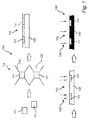
- Fig. 1 is a schematic illustration of a method 100 for manufacturing a lighting module 150.
- the method 100 comprises the step of providing a light-source assembly 110 comprising a plurality of light sources 111 (hereafter denoted LEDs) being electrically connected to a carrier 112.
- the carrier 112 is provided as a wire grid upon which the LEDs 111 are connected, wherein the wire grid has the shape of a chicken wire.
- the wire grid has the shape of a chicken wire.
- Each of the LEDs 111 has a light-emitting (i.e. translucent) surface on a top portion of the LEDs 111.
- the method 100 further comprises the step of providing a heat sink material 120 in a fluid state, whereir said heat sink material comprises at least one ceramic material.
- Preferred ceramics are e.g. clay, concrete, quartz, porcelain, etc., as these ceramic materials are both inexpensive and possess heat-conductive properties, thereby being highly advantageous for the use as a cost-effective heat sink material 120 in the present method 100 and lighting module 150.
- Other ceramics which may be considered as heat sink material 120 are oxide ceramics (e.g. alumina, beryllia, ceria, zirconia), nonoxide ceramics (carbide, boride, nitride, silicide) and composite materials, e.g. combinations of oxide and nonoxide ceramics.
- the heat sink material 120 in the fluid state may be supplied to a mould or the like arranged for holding and/or shaping the heat sink material.
- the method 100 further comprises the step of embedding 130 the light-source assembly 110 into the heat sink material 120.
- the embedding 130 is performed in such a way that the carrier 110 and a part of each of the LEDs 111 are covered by the heat sink material 120 while the light-emitting surface 113 of each of the LEDs 111 is uncovered by the heat sink material 120.
- the embedding 130 may be performed by applying pressure to the light-source assembly 110 such that it is pressed into the heat sink material 120.
- the method 100 comprises the step of solidifying 140 the heat sink material 120, i.e. making the heat sink material solid 140.
- the step of solidifying 140 the heat sink material 120 maybe performed by using a step comprising polymerizing, heating (baking) or pressurizing (or a combination thereof) of the heat sink material 120. After the heat sink material 120 is made solid, it provides the light-source assembly 110 (i.e. the carrier 110 and the LEDs 111) with the required stiffness for fixation.
- Figs. 2a-b are schematic illustrations from above of the lighting module 150, comprising the light-source assembly 110 embedded into the solidified heat sink material 120.
- the wire grid of the carrier 112 of the light-source assembly 110 has the shape of a chicken wire.
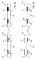
- Figs. 3a-c are schematic side-view illustrations of the lighting module 150 comprising the light-source assembly 110 embedded into the solidified heat sink material 120.
- a phosphor layer 301 is applied to each of the LEDs 111 before embedding the lighting module 110 in the heat sink material 120.
- the phosphor layer(s) 301 is (are) applied for the purpose of converting a light of a first wavelength to a light of a second wavelength.
- the resulting color of one (or more) of the LEDs 111 after applying the phosphor layer 301 maybe any color, e.g. red (e.g. leftmost LED 111 in Fig. 3a ), whereas the resulting color of any other (or more) of the LEDs 111 may be the same, or any other color, e.g. green (e.g. rightmost LED 111 in Fig. 3a ).
- a phosphor layer 301 is instead applied to the LEDs 111 after embedding the lighting module 110 in the heat sink material 120.
- the phosphor layers 301 are applied as separate layers on each of the LEDs 111, whereas in Fig. 3c , the phosphor layer 301 is instead applied to the surface of the lighting module 150 and thereafter coated (and/or spread and/or smeared) onto the surface of the lighting module 150 by means of a coating element 302.
- Figs. 4a-b are schematic side-view illustrations of the lighting module 150 comprising the light-source assembly 110 embedded into the solidified heat sink material 120.
- a dome-shaped optical structure 401 is applied to each LED 111 before embedding the lighting-source assembly 110 in the heat sink material 120.
- the optical structures 401 may instead be applied to the LEDs 111 after embedding the light-source assembly 110 in the heat sink material 120, which is shown in Fig. 4b .
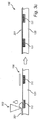
- Fig. 5 is again a schematic side-view illustration of the lighting module 150 comprising the light-source assembly 110 embedded into the solidified heat sink material 120.
- a protective layer 501 is applied around the LEDs 111 for protecting the LEDs 111 when subjected to (possible) further manufacturing steps.
- Fig. 6 is a schematic side-view illustration of an embodiment of the method of manufacturing the lighting module 150.
- the light-source assembly 110 is pressed into the heat sink material 120 by means of a profile-shaped pressing means 601.
- the pressing means 601 comprises steps, such that when the pressing means 601 is pressed into the heat sink material 120 in its fluid state, the resulting shape of the lighting module 150 and/or heat sink material 120 is formed after the step-like profile of the pressing means 601.
- the resulting lighting module 150 and heat sink material 120 maybe shaped such that the LEDs 111 of the lighting module 150 are provided in a lower portion of the heat sink material 120 than the surrounding heat sink material 120.
- This profile of the heat sink material 120 may, as an example, provide a mixing chamber 602 for the lighting module 150.
- the pressing means 601 may comprise substantially any shape for forming a desired shape/profile in the fluid heat sink material 120.
- any step of the method of manufacturing the lighting module 150 as described may be combined with any other step (or steps) as described and/or be applied to any number of components (e.g. LEDs 111).
- a lighting module 150 has been provided with multiple mixing chambers 602, e.g. after having been subjected to a profile-shaped pressing means.
- a phosphor layer 301 is applied to the lighting module 150, providing a space of the mixing chambers 602 between the LEDs 111 and the phosphor layer 301.
- Fig. 8 is a schematic illustration of an illumination device 200 comprising a lighting module 150 with a heat sink material 120.
- the illumination device 200 further comprises a connector 201 which is electrically connected to the carrier (not shown) of the lighting module 150.
- the connector 201 is arranged for electrical connection, e.g. to a socket, such that the illumination device 200 may be connected to a luminaire such as a lamp or the like.
- one or more reflecting elements 202 may be provided in the illumination device 200.
- Fig. 8 shows a cut view of a reflecting element 202 projecting from the heat sink material 120 and being arranged to reflect light from the light sources of the lighting module 150. It will be appreciated that although the illumination device 200 is shown in Fig. 8 in a shape similar to a light bulb, the illumination device 200 may also take on virtually any other shape, e.g. for the purpose of being arranged in a luminaire to be suspended from a ceiling.
- the shapes and sizes of the LEDs 111, carrier 112, heat sink material 120 after solidifying, optical elements 401, phosphor layer 301, and so on, maybe different from that shown.
Landscapes
- Engineering & Computer Science (AREA)
- Microelectronics & Electronic Packaging (AREA)
- Power Engineering (AREA)
- Physics & Mathematics (AREA)
- Computer Hardware Design (AREA)
- General Engineering & Computer Science (AREA)
- Manufacturing & Machinery (AREA)
- Optics & Photonics (AREA)
- General Physics & Mathematics (AREA)
- Condensed Matter Physics & Semiconductors (AREA)
- Arrangement Of Elements, Cooling, Sealing, Or The Like Of Lighting Devices (AREA)
- Non-Portable Lighting Devices Or Systems Thereof (AREA)
- Led Device Packages (AREA)
- Fastening Of Light Sources Or Lamp Holders (AREA)
Description
- The present invention relates to a lighting module and to a method of manufacturing a lighting module.
- Common to light sources such as light-emitting diodes (LEDs), light bulbs, laser diodes and lamps is that the light sources emit heat. Light-emitting arrangements comprising a plurality of light sources, e.g. for use in a display or in an illumination device, may generate a quick rise of the temperature of the light-emitting arrangement, especially if many light sources are driven at the same time. The effect of heat may be detrimental to the light sources, and their operation may become erratic and unstable. As a consequence, the light from the light source may flicker, causing degradation of the quality of the display or illumination. Hence, thermal management is an important issue to prevent thermal damage of the light sources, and it is necessary to dissipate excess heat in order to maintain the reliability of the light-emitting arrangement and to prevent premature failure of the light sources.
- However, the manufacture of heat sinks for the dissipation of heat for light-emitting arrangements is associated with relatively high costs, and a large fraction of the cost of light-emitting arrangements is related to the heat sinks and the procedure of assembling together the light sources with the heat sink.
- In the light of the above observations, there is an increasing need for a cost-effective manufacture of light-emitting arrangements having heat dissipation properties.
-
DE 10 2004 057 804 discloses a housing body for a semiconductor chip and a method for the production thereof. A lead frame, having a mounting surface for the arrangement of a semiconductor chip, is applied with an adhesive layer and placed into a mould. The lead frame may further be provided with a coating of silver, gold or nickel-palladium. A ceramic material such as aluminum oxide or zirconium oxide, is poured into the mould such that the material surrounds the lead frame and forms a housing body of the lead frame. - However, the method of producing the housing body for each semiconductor chip is inefficient, complicated and circumstantial. As a consequence, the manufactured product becomes relatively expensive. Hence, alternative solutions for the manufacture of electronic products having an effective heat dissipation are of interest, such that a more cost-effective manufacture, as well as the product resulting from the manufacture, is provided.
-
WO 2007/149362 A1 discloses a method of placing LED bare dies directly from a wafer tape into a melt adhesive. A light strip is made by providing electrical contact with the conductive surface of a top substrate, so that a connection can be made through the buss to the conductive surface and to the LED die. The buss and the conductive bottom substrate provide a conductive pathway to each LED such that the light strip can be cut anywhere along its length. An electrical connection to the buss and the conductive bottom substrate of each cut strip energizes the LEDs and generates light. -
WO 2010/035206 A1 discloses a light emitting diode arranged on a submount, said device having a lateral circumference surface and a top surface, and an optically active coating layer, said coating layer covering along at least a part of said circumference surface, extending from the submount to said top surface, and essentially not covering the top surface. - It is an object of the present invention to mitigate the above problems and to provide a method for manufacturing a lighting module, as well as a lighting module, which is cost-effective.
- This and other objects are achieved by providing a lighting module and a method having the features defined in the independent claims. Preferred embodiments are defined in the dependent claims.
- Hence, according to a first aspect of the present invention, there is provided a method of manufacturing a lighting module. The method comprises the step of providing a heat sink material in a fluid state. Further, the method comprises the step of providing a light-source assembly comprising a plurality of light sources being electrically connected to an electrically conductive carrier, wherein each of the light sources has a light-emitting surface. Further, the method comprises the step of embedding the light-source assembly into the heat sink material such that the electrically conductive carrier and a part of each of the light sources are covered by the heat sink material while the light-emitting surface of each of the light sources is uncovered by the heat sink material. Further, the method comprises the step of solidifying the heat sink material.
- According to a second aspect of the present invention, there is provided a lighting module, comprising a light-source assembly. The light-source assembly comprises a plurality of light sources being electrically connected to an electrically conductive carrier, wherein each of the light sources has a light-emitting surface. The lighting module further comprises a heat sink material, wherein the electrically conductive carrier and a part of each of the light sources are covered by the heat sink material while the light-emitting surface of each of the light sources is uncovered by the heat sink material.
- By the term "fluid state", it is here meant a state of the heat sink material which is able to conform to the light-source assembly. More specifically, it will be appreciated that in this context, the "fluid state" of the heat sink material represents a liquid heat sink material with a relatively high viscosity, wherein the heat sink material is in a non-gaseous state.
- By the term "carrier", it is here meant substantially any electrically conductive element for supplying electricity to the light sources.
- By the term "light-emitting surface", it is here meant a surface from which light is emitted by the light-source.
- By the term "solidifying", it is here meant to make a material solid, for example through hardening, curing and/or tempering.
- By the term "luminaire", it is here meant an electrical device for creating artificial light, e.g. a light fixture, a light fitting or the like.
- Thus, the present invention is based on the idea of providing a method for manufacturing a lighting module, wherein a light-source assembly, comprising a plurality of light sources being electrically connected to an electrically conductive carrier, is partly embedded (immersed) into the fluid heat sink material. The light-source assembly is embedded such that the electrically conductive carrier and a part of each of the light sources are covered (embedded) by the heat sink material, whereas the light-emitting surface of each of the light sources remains uncovered by the heat sink material. Then, the heat sink material is solidified to fix the light-source assembly in the heat sink material. The present invention thereby provides an efficient and cost-effective method of manufacturing a lighting module comprising a light-source assembly and a heat sink structure arranged to dissipate heat generated by the light sources, when in operation.
- An advantage of various embodiments of the present invention is that the method provides good thermal contact between the light sources (e.g. LEDs), the electrically conductive carrier and the heat sink material in a rational and production-friendly way. Moreover, a large quantity of light sources maybe embedded either simultaneously or after each other into the heat sink material, by machine or by hand. The present method is thereby more efficient compared to methods wherein electrical components are held in a mould, or the like, and material is filled into the mould to surround the components. Whereas methods of this latter kind result in a slow and troublesome procedure, and especially when components are processed one-by-one, the present invention provides an easier, faster and/or more cost-effective method for providing heat sinks structures for the dissipation of heat from light sources.
- Another advantage is that the electrically conductive carrier, to which the light sources are connected, may be adapted to e.g. the size, number and concentration of the light sources which are to be embedded and/or be adapted to the properties of the heat sink material. Hence, the carrier to an even further extent facilitates the embedding of the light-source assembly into the fluid (soft, viscous) heat sink material.
- Another advantage achievable through various embodiments of the present invention is that fewer process steps and/or less material is needed in the method when providing the light source assembly with the heat sink material compared to methods in the prior art. As a consequence, the present method provides a more cost-effective method for manufacturing the lighting module as well as an inexpensive lighting module. Furthermore, the method provides a more environmental-friendly approach compared to prior art methods, as less material is used when manufacturing the lighting module.
- Another advantage obtainable through various embodiments of the present invention is that the heat sink material may be chosen to be a cost-effective (inexpensive) material, having at least sufficient and/or satisfactory heat-sinking properties. Hence, by the choice of heat sink material, the method for manufacturing the lighting module, as well as the lighting module itself, becomes even more cost-effective compared to methods/products in the prior art. Furthermore, as less material may be used when manufacturing the lighting module compared to prior art methods, the method of the present invention even further decreases manufacturing costs.
- According to an embodiment of the present invention, the heat sink material may be non-transparent. Hence, in this embodiment, the heat sink material is non-translucent, and the light emitted from the light sources is partly or completely transmitted through the light-emitting surface of the light sources. Since the light-emitting surface is left uncovered by the heat sink material, the embodiment is advantageous in that non-transparent heat sink materials may be used, which reduces the cost considerably as compared to transparent heat sink materials, which would have been necessary had the light-emitting surface been covered by the heat sink material.
- According to the present invention, the heat sink material comprises at least one ceramic material. An advantage is that ceramic materials are relatively inexpensive and easily accessible and/or producible, even further contributing to the cost-effectiveness of the present method. A further advantage of is that ceramic materials provide a satisfactory and/or sufficient heat conductivity for the purpose of dissipating heat from the light sources of the lighting module of the present invention during operation.
- According to an embodiment of the present invention, the at least one ceramic material may be chosen from a group consisting of clay, concrete and porcelain. The ceramic materials clay, concrete and/or porcelain are highly advantageous for the use as a cost-effective heat sink material in the present method and lighting module, as the ceramic materials are both inexpensive and possess heat-conductive properties. Other ceramics which may be considered as heat sink material are oxide ceramics (e.g. alumina, beryllia, ceria, zirconia), nonoxide ceramics (carbide, boride, nitride, silicide) and composite materials, e.g. combinations of oxide and nonoxide ceramics.
- According to an embodiment of the present invention, the electrically conductive carrier may comprise a wire grid. By the term "wire grid", it is here meant substantially any grid/mesh-like structure, framework, or the like. The wire grid may comprise wires, lines and/or cables. An advantage of the present embodiment is that the grid structure of the carrier saves material compared to a carrier having a more homogeneous (unitary) structure (e.g. a circuit board or the like), thereby providing an even more cost-efficient method and lighting module. Furthermore, as the present embodiment uses less material, an even more environmental-friendly method and lighting module is provided. The present embodiment is advantageous in that the carrier, comprising a wire grid, provides a lighter lighting module compared to more homogeneous carriers. Furthermore, the grid-like structure of the carrier of the present embodiment allows for an improved embedding of the carrier into the heat sink material compared to other arrangements in the prior art. Consequently, the carrier is able to provide an improved heat transfer to the heat sink material.
- The electrically conductive carrier may further comprise a lead frame. An advantage of the lead frame is that the electrically conductive carrier may provide a firm support for the light sources. Further, the lead-frame carrier may have a sparse construction in which it provides an even more cost-efficient method and lighting module, compared to a carrier having a more homogeneous structure (e.g. a circuit board or the like), in terms of material savings. The lead frame is further advantageous in that the sparse construction of the lead frame allows for an improved embedding of the carrier into the heat sink material compared to other prior art arrangements. The carrier, which may be provided in various thicknesses and sizes, is thereby able to provide an improved heat transfer to the heat sink material.
- The light sources of the lighting module may be light-emitting diodes (LED) or laser diodes. The use of LEDs and laser diodes is beneficial in that they present several advantages over incandescent light sources, including lower energy consumption, longer lifetime, improved robustness, smaller size and the use of more environmental-friendly materials for an improved recycling. Hence, an even more efficient and cost-effective method and lighting module may be provided.
- According to an embodiment of the present invention, the method may further comprise the step of applying a phosphor layer on at least one of the light sources. The applying of a phosphor material is advantageous in that it may be used to convert a light of a first wavelength range to a light of a second wavelength range, e.g. a monochromatic light from a blue or ultraviolet (UV) LED to a white light. The present embodiment is further advantageous in that the phosphor layer may efficiently and easily be applied on the light-emitting surface of the light source, either before embedding the light-source assembly into the heat sink material or after the light-source assembly has been embedded in the heat sink material. Hence, the embodiment thereby even further improves the (cost)-efficiency of the method and the lighting module according to various embodiments of the present invention.
- According to an embodiment of the present invention, the method further comprises the step of applying an optical structure on at least one of the light sources. The optical structure, e.g. a dome structure, applied on the light-emitting surface of the light source may further efficiently improve the light distribution. An advantage of the present embodiment is that the optical structure may efficiently and easily be applied on the light-emitting surface of the light source, either before or after the embedding the light-source assembly into the heat sink material, leading to an even more efficient method of manufacturing the lighting module.
- According to an embodiment of the present invention, the method may further comprise the step of applying a protective layer on at least one of the light sources. An advantage of the present embodiment is that the protective layer efficiently protects the light sources in case further processing steps are performed. The protective layer may be applied on the light source either before or after embedding the light-source assembly into the heat sink material, and the (cost)-efficiency of the method and the lighting module of the present invention may thereby be even further improved.
- According to an embodiment of the present invention, the step of embedding may comprise the step of pressing the light-source assembly into the heat sink material in the fluid state by means of a pressing means comprising a base portion and at least one protruding portion which protrudes from the base portion. The at least one protruding portion is arranged to press the at least one light source into the heat sink material at the light-emitting surface of the at least one light source to prevent the heat sink material from covering the light-emitting surface.
- The pressing means is hereby arranged to press the light-source assembly into the heat sink material such that the means forms the heat sink material according to the profile of the means. An advantage of the present embodiment is that the pressing means of the embodiment of the present invention may press the light-source assembly into the heat sink material while simultaneously forming the heat sink material in the fluid state into a desired form. Hence, the present embodiment even further contributes to the cost-efficiency of the method of manufacturing the lighting module.
- According to an embodiment of the present invention, the heat sink material may be shaped by the pressing means upon the pressing of the light-source assembly into the heat sink material to form a cavity around the at least one light source. An advantage of the present embodiment is that the heat sink material hereby provides a cavity of the at least one light source, which e.g. may serve as a mixing chamber for the lighting module.
- According to an embodiment of the present invention, the step of solidifying may comprise the step of polymerizing the heat sink material. In other words, the fluid heat sink, into which the light-source assembly has been embedded, is hardened by polymerization. The efficiency of polymerization provides the advantage that solidifying the heat sink material by means of this technique even further contributes to the cost-efficiency of the method of the present invention.
- According to an embodiment of the present invention, the step of solidifying may comprise the step of heating the heat sink material. In other words, after the light-source assembly has been embedded into the fluid heat sink material, the heat sink material is hardened by heating (baking). The present embodiment is advantageous in that solidifying the heat sink material by applying heat implies an easy, efficient and inexpensive solidification of the heat sink material, thereby providing an even more cost-efficient method of the present invention.
- According to an embodiment of the present invention, the step of solidifying may comprise the step of pressurizing the heat sink material. In this embodiment, the fluid heat sink, into which the light-source assembly has been embedded, is hardened by applying (additional) pressure to the heat sink material. The applied pressure lowers the melting temperature of the heat sink material, and provides an efficient solidification of the heat sink material.
- According to an embodiment of the present invention, there is provided an illumination device, comprising at least one lighting module according to the previously described embodiment. The illumination device further comprises a connector being electrically connected to the carrier of the at least one lighting module, wherein the connector is arranged for connection to a luminaire. Hence, in the present embodiment, the lighting module may be arranged in a illumination device for connection to a luminaire such as a lamp or the like. The present embodiment is advantageous in that the concept of the cost-effective lighting module, comprising a light-source assembly and a heat sink structure arranged to dissipate heat generated by the light sources, is further applicable for illumination devices for connection to luminaires.
- It will be appreciated that the specific embodiments and any additional features described above with reference to the method of manufacturing the lighting module are likewise applicable and combinable with the lighting module according to the second aspect of the present invention.
- These and other aspects of the present invention will now be described in more detail, with reference to the appended drawings showing a currently preferred embodiment of the invention, wherein:
-
Fig. 1 is a schematic illustration of a method of manufacturing a lighting module according to an embodiment of the present invention, -
Figs. 2a-b are schematic views from above of a lighting module according to an embodiment of the present invention, and -
Figs. 3-7 are schematic side-view illustrations of a method of manufacturing a lighting module according to embodiments of the present invention, and -
Fig. 8 is a schematic illustration of an illumination device according to an embodiment of the present invention. - In the following description, the present invention is described with reference to a method of manufacturing a lighting module.
-
Fig. 1 is a schematic illustration of amethod 100 for manufacturing alighting module 150. Themethod 100 comprises the step of providing a light-source assembly 110 comprising a plurality of light sources 111 (hereafter denoted LEDs) being electrically connected to acarrier 112. Here, thecarrier 112 is provided as a wire grid upon which theLEDs 111 are connected, wherein the wire grid has the shape of a chicken wire. However, it will be appreciated that substantially any shape of the wire grid may be feasible. Each of theLEDs 111 has a light-emitting (i.e. translucent) surface on a top portion of theLEDs 111. Themethod 100 further comprises the step of providing aheat sink material 120 in a fluid state, whereir said heat sink material comprises at least one ceramic material. Preferred ceramics are e.g. clay, concrete, quartz, porcelain, etc., as these ceramic materials are both inexpensive and possess heat-conductive properties, thereby being highly advantageous for the use as a cost-effectiveheat sink material 120 in thepresent method 100 andlighting module 150. Other ceramics which may be considered asheat sink material 120 are oxide ceramics (e.g. alumina, beryllia, ceria, zirconia), nonoxide ceramics (carbide, boride, nitride, silicide) and composite materials, e.g. combinations of oxide and nonoxide ceramics. Theheat sink material 120 in the fluid state may be supplied to a mould or the like arranged for holding and/or shaping the heat sink material. - The
method 100 further comprises the step of embedding 130 the light-source assembly 110 into theheat sink material 120. The embedding 130 is performed in such a way that thecarrier 110 and a part of each of theLEDs 111 are covered by theheat sink material 120 while the light-emitting surface 113 of each of theLEDs 111 is uncovered by theheat sink material 120. The embedding 130 may be performed by applying pressure to the light-source assembly 110 such that it is pressed into theheat sink material 120. Further, themethod 100 comprises the step of solidifying 140 theheat sink material 120, i.e. making the heat sink material solid 140. The step of solidifying 140 theheat sink material 120 maybe performed by using a step comprising polymerizing, heating (baking) or pressurizing (or a combination thereof) of theheat sink material 120. After theheat sink material 120 is made solid, it provides the light-source assembly 110 (i.e. thecarrier 110 and the LEDs 111) with the required stiffness for fixation. -
Figs. 2a-b are schematic illustrations from above of thelighting module 150, comprising the light-source assembly 110 embedded into the solidifiedheat sink material 120. Here, the wire grid of thecarrier 112 of the light-source assembly 110 has the shape of a chicken wire. -
Figs. 3a-c are schematic side-view illustrations of thelighting module 150 comprising the light-source assembly 110 embedded into the solidifiedheat sink material 120. InFig. 3a , aphosphor layer 301 is applied to each of theLEDs 111 before embedding thelighting module 110 in theheat sink material 120. The phosphor layer(s) 301 is (are) applied for the purpose of converting a light of a first wavelength to a light of a second wavelength. As an example, the resulting color of one (or more) of theLEDs 111 after applying thephosphor layer 301 maybe any color, e.g. red (e.g.leftmost LED 111 inFig. 3a ), whereas the resulting color of any other (or more) of theLEDs 111 may be the same, or any other color, e.g. green (e.g.rightmost LED 111 inFig. 3a ). - In
Figs. 3b-c , aphosphor layer 301 is instead applied to theLEDs 111 after embedding thelighting module 110 in theheat sink material 120. InFig. 3b , the phosphor layers 301 are applied as separate layers on each of theLEDs 111, whereas inFig. 3c , thephosphor layer 301 is instead applied to the surface of thelighting module 150 and thereafter coated (and/or spread and/or smeared) onto the surface of thelighting module 150 by means of acoating element 302. -
Figs. 4a-b are schematic side-view illustrations of thelighting module 150 comprising the light-source assembly 110 embedded into the solidifiedheat sink material 120. InFig. 4a , a dome-shapedoptical structure 401 is applied to eachLED 111 before embedding the lighting-source assembly 110 in theheat sink material 120. Alternatively, theoptical structures 401 may instead be applied to theLEDs 111 after embedding the light-source assembly 110 in theheat sink material 120, which is shown inFig. 4b . -
Fig. 5 is again a schematic side-view illustration of thelighting module 150 comprising the light-source assembly 110 embedded into the solidifiedheat sink material 120. Here, aprotective layer 501 is applied around theLEDs 111 for protecting theLEDs 111 when subjected to (possible) further manufacturing steps. -
Fig. 6 is a schematic side-view illustration of an embodiment of the method of manufacturing thelighting module 150. The light-source assembly 110 is pressed into theheat sink material 120 by means of a profile-shapedpressing means 601. Here, the pressing means 601 comprises steps, such that when thepressing means 601 is pressed into theheat sink material 120 in its fluid state, the resulting shape of thelighting module 150 and/orheat sink material 120 is formed after the step-like profile of thepressing means 601. For example, the resultinglighting module 150 andheat sink material 120 maybe shaped such that theLEDs 111 of thelighting module 150 are provided in a lower portion of theheat sink material 120 than the surroundingheat sink material 120. This profile of theheat sink material 120 may, as an example, provide amixing chamber 602 for thelighting module 150. However, it will be appreciated that the pressing means 601 may comprise substantially any shape for forming a desired shape/profile in the fluidheat sink material 120. - It will be appreciated that any step of the method of manufacturing the
lighting module 150 as described may be combined with any other step (or steps) as described and/or be applied to any number of components (e.g. LEDs 111). For example, inFig. 7 , alighting module 150 has been provided with multiple mixingchambers 602, e.g. after having been subjected to a profile-shaped pressing means. Furthermore, after the mixingchambers 602 have been provided, aphosphor layer 301 is applied to thelighting module 150, providing a space of the mixingchambers 602 between theLEDs 111 and thephosphor layer 301. -
Fig. 8 is a schematic illustration of anillumination device 200 comprising alighting module 150 with aheat sink material 120. Theillumination device 200 further comprises aconnector 201 which is electrically connected to the carrier (not shown) of thelighting module 150. Theconnector 201 is arranged for electrical connection, e.g. to a socket, such that theillumination device 200 may be connected to a luminaire such as a lamp or the like. Optionally, one or more reflectingelements 202 may be provided in theillumination device 200.Fig. 8 shows a cut view of a reflectingelement 202 projecting from theheat sink material 120 and being arranged to reflect light from the light sources of thelighting module 150. It will be appreciated that although theillumination device 200 is shown inFig. 8 in a shape similar to a light bulb, theillumination device 200 may also take on virtually any other shape, e.g. for the purpose of being arranged in a luminaire to be suspended from a ceiling. - Even though the invention has been described with reference to specific exemplifying embodiments thereof, many different alterations, modifications and the like will become apparent for those skilled in the art. The described embodiments are therefore not intended to limit the scope of the invention, as defined by the appended claims.
- For example, the shapes and sizes of the
LEDs 111,carrier 112,heat sink material 120 after solidifying,optical elements 401,phosphor layer 301, and so on, maybe different from that shown.
Claims (14)
- A method (100) of manufacturing a lighting module (150), comprising the steps of:providing a heat sink material (120) in a fluid state;providing a light-source assembly (110) comprising a plurality of light sources being electrically connected to an electrically conductive carrier (112), each of said light sources (111) having a light-emitting surface (113);embedding (130) said light-source assembly into said heat sink material such that said electrically conductive carrier and apart of each of said light sources are covered by said heat sink material while said light-emitting surface of each of said light sources is uncovered by said heat sink material; andsolidifying (140) said heat sink material,characterized in that said heat sink material (120) comprises at least one ceramic material.
- The method (100) as claimed in claim 1, wherein said heat sink material (120) is non-transparent.
- The method (100) as claimed in claim 1, wherein said at least one ceramic material is chosen from a group consisting of clay, concrete and porcelain.
- The method (100) as claimed in any one of the preceding claims, wherein said electrically conductive carrier (112) comprises a wire grid.
- The method (100) as claimed in any one of the preceding claims, further comprising the step of applying a phosphor layer (301) on at least one of said light sources(111).
- The method (100) as claimed in any one of the preceding claims, further comprising the step of applying an optical structure on at least one of said light sources (111).
- The method (100) as claimed in any one of the preceding claims, further comprising the step of applying a protective layer (501) on at least one of said light sources (111).
- The method (100) as claimed in any one of the preceding claims, wherein said step of embedding (130) comprises the step of:pressing said light-source assembly (110) into said heat sink material (120) in said fluid state by means of a pressing means (601) comprising a base portion and at least one protruding portion which protrudes from said base portion, wherein said at least one protruding portion is arranged to press said at least one light source (111) into said heat sink material at said light-emitting surface (113) of the at least one light source to prevent said heat sink material from covering said light-emitting surface.
- The method (100) as claimed in claim 8, wherein said heat sink material (120) is shaped by said pressing means (601) upon said pressing of said light-source assembly (110) into said heat sink material to form a cavity around said at least one light source (111).
- The method (100) as claimed in any one of the preceding claims, wherein said step of solidifying (140) comprises the step of:polymerizing said heat sink material (120).
- The method (100) as claimed in any one of claims 1-9, wherein said step of solidifying (140) comprises the step of:heating said heat sink material (120).
- The method (100) as claimed in any one of claims 1-9, wherein said step of solidifying (140) comprises the step of:pressurizing said heat sink material (120).
- A lighting module (150), comprising:a light-source assembly (110) comprising a plurality of light sources (111) being electrically connected to an electrically conductive carrier (112), each of said light sources having a light-emitting surface (113), anda heat sink material (120), wherein said electrically conductive carrier and a part of each of said light sources are covered by said heat sink material while said light-emitting surface of each of said light sources is uncovered by said heat sink material, characterized in that said heat sink material (120) comprises at least one ceramic material.
- An illumination device (200), comprising:at least one lighting module (150) as claimed in claim 13, wherein said illumination device further comprises a connector (201) being electrically connected to said carrier (112) of said at least one lighting module, wherein said connector is arranged for connection to a luminaire.
Applications Claiming Priority (2)
| Application Number | Priority Date | Filing Date | Title |
|---|---|---|---|
| US201261607058P | 2012-03-06 | 2012-03-06 | |
| PCT/IB2013/051563 WO2013132389A1 (en) | 2012-03-06 | 2013-02-27 | Lighting module and method of manufacturing a lighting module |
Publications (2)
| Publication Number | Publication Date |
|---|---|
| EP2823517A1 EP2823517A1 (en) | 2015-01-14 |
| EP2823517B1 true EP2823517B1 (en) | 2016-04-27 |
Family
ID=48093044
Family Applications (1)
| Application Number | Title | Priority Date | Filing Date |
|---|---|---|---|
| EP13716059.4A Active EP2823517B1 (en) | 2012-03-06 | 2013-02-27 | Lighting module and method of manufacturing a lighting module |
Country Status (5)
| Country | Link |
|---|---|
| US (1) | US9777890B2 (en) |
| EP (1) | EP2823517B1 (en) |
| JP (1) | JP6559424B2 (en) |
| CN (1) | CN104160522B (en) |
| WO (1) | WO2013132389A1 (en) |
Families Citing this family (2)
| Publication number | Priority date | Publication date | Assignee | Title |
|---|---|---|---|---|
| US20150131295A1 (en) * | 2013-11-12 | 2015-05-14 | GE Lighting Solutions, LLC | Thin-film coating for improved outdoor led reflectors |
| US11562982B2 (en) * | 2019-04-29 | 2023-01-24 | Taiwan Semiconductor Manufacturing Company, Ltd. | Integrated circuit packages and methods of forming the same |
Family Cites Families (30)
| Publication number | Priority date | Publication date | Assignee | Title |
|---|---|---|---|---|
| JPH03151674A (en) | 1989-11-08 | 1991-06-27 | Sharp Corp | Semiconductor device |
| JPH06326144A (en) | 1993-05-17 | 1994-11-25 | Toshiba Corp | Manufacture of resin-sealed semiconductor device |
| US5528474A (en) * | 1994-07-18 | 1996-06-18 | Grote Industries, Inc. | Led array vehicle lamp |
| US6318886B1 (en) * | 2000-02-11 | 2001-11-20 | Whelen Engineering Company | High flux led assembly |
| JP4100946B2 (en) * | 2002-03-27 | 2008-06-11 | 松下電器産業株式会社 | Lighting device |
| JP2010093285A (en) | 2003-02-28 | 2010-04-22 | Sanyo Electric Co Ltd | Method of manufacturing semiconductor device |
| CN100428507C (en) | 2003-06-06 | 2008-10-22 | 夏普株式会社 | Optical transmitter |
| JP2005159296A (en) | 2003-11-06 | 2005-06-16 | Sharp Corp | Package structure of optodevice |
| US7858994B2 (en) | 2006-06-16 | 2010-12-28 | Articulated Technologies, Llc | Solid state light sheet and bare die semiconductor circuits with series connected bare die circuit elements |
| US7044620B2 (en) * | 2004-04-30 | 2006-05-16 | Guide Corporation | LED assembly with reverse circuit board |
| JP2006100633A (en) * | 2004-09-30 | 2006-04-13 | Toyoda Gosei Co Ltd | Led lighting device |
| DE102004057804B4 (en) | 2004-11-30 | 2010-04-08 | Osram Opto Semiconductors Gmbh | Housing body for a semiconductor chip of cast ceramic with reflective effect and method for its production |
| WO2006093889A2 (en) | 2005-02-28 | 2006-09-08 | Color Kinetics Incorporated | Configurations and methods for embedding electronics or light emitters in manufactured materials |
| JP4375564B2 (en) | 2005-03-17 | 2009-12-02 | 日本電気株式会社 | Sealing resin composition, electronic component device sealed with sealing resin composition, and method for repairing semiconductor element |
| TWI256454B (en) * | 2005-06-03 | 2006-06-11 | Au Optronics Corp | Light module |
| JP5192646B2 (en) | 2006-01-16 | 2013-05-08 | Towa株式会社 | Optical element resin sealing method, resin sealing apparatus, and manufacturing method thereof |
| WO2007122566A1 (en) | 2006-04-25 | 2007-11-01 | Koninklijke Philips Electronics N.V. | Led array grid, method and device for manufacturing said grid and led component for use in the same |
| TWI318792B (en) * | 2006-09-19 | 2009-12-21 | Phoenix Prec Technology Corp | Circuit board structure having embedded semiconductor chip and fabrication method thereof |
| US20080298033A1 (en) * | 2007-06-01 | 2008-12-04 | Smith Roy A | Power supply platform and electronic component |
| WO2009078301A1 (en) | 2007-12-14 | 2009-06-25 | Sony Chemical & Information Device Corporation | Photosemiconductor package sealing resin material |
| CN101463985B (en) * | 2007-12-21 | 2010-12-08 | 富士迈半导体精密工业(上海)有限公司 | LED lamp |
| JP2009231584A (en) | 2008-03-24 | 2009-10-08 | Japan Gore Tex Inc | Method of manufacturing led substrate and the led substrate |
| US8461613B2 (en) | 2008-05-27 | 2013-06-11 | Interlight Optotech Corporation | Light emitting device |
| US8957428B2 (en) * | 2008-09-25 | 2015-02-17 | Koninklijke Philips N.V. | Coated light emitting device and method for coating thereof |
| DE102009012517A1 (en) | 2009-03-10 | 2010-09-16 | Osram Opto Semiconductors Gmbh | Optoelectronic semiconductor component |
| JP5121783B2 (en) * | 2009-06-30 | 2013-01-16 | 株式会社日立ハイテクノロジーズ | LED light source, manufacturing method thereof, exposure apparatus using LED light source, and exposure method |
| JP5683799B2 (en) * | 2009-09-14 | 2015-03-11 | スターライト工業株式会社 | LED heat sink for automobile |
| KR101144202B1 (en) * | 2009-11-02 | 2012-05-10 | 삼성전기주식회사 | Light emitting diode embedded printed circuit board having |
| JP4681071B1 (en) * | 2009-12-17 | 2011-05-11 | 株式会社スズデン | lighting equipment |
| BE1019763A3 (en) | 2011-01-12 | 2012-12-04 | Sioen Ind | METHOD FOR EMBEDDING LED NETWORKS. |
-
2013
- 2013-02-27 JP JP2014560476A patent/JP6559424B2/en active Active
- 2013-02-27 US US14/381,240 patent/US9777890B2/en active Active
- 2013-02-27 EP EP13716059.4A patent/EP2823517B1/en active Active
- 2013-02-27 WO PCT/IB2013/051563 patent/WO2013132389A1/en active Application Filing
- 2013-02-27 CN CN201380012842.2A patent/CN104160522B/en active Active
Also Published As
| Publication number | Publication date |
|---|---|
| CN104160522B (en) | 2017-12-22 |
| JP6559424B2 (en) | 2019-08-14 |
| WO2013132389A1 (en) | 2013-09-12 |
| EP2823517A1 (en) | 2015-01-14 |
| US9777890B2 (en) | 2017-10-03 |
| JP2015511066A (en) | 2015-04-13 |
| US20150103521A1 (en) | 2015-04-16 |
| CN104160522A (en) | 2014-11-19 |
Similar Documents
| Publication | Publication Date | Title |
|---|---|---|
| JP4789672B2 (en) | Light emitting device and lighting device | |
| JP5658394B2 (en) | Lamp and lighting device | |
| US10094523B2 (en) | LED assembly | |
| KR101209759B1 (en) | Semiconductor light emitting module and method for manufacturing the same | |
| JP5219445B2 (en) | Light emitting diode device | |
| JP6089309B2 (en) | Lamp and lighting device | |
| WO2011136236A1 (en) | Leadframe, wiring board, light emitting unit, and illuminating apparatus | |
| JP4948818B2 (en) | Light emitting device and lighting device | |
| TWM437919U (en) | Light emission device | |
| JP2016171147A (en) | Light emission device and luminaire | |
| TW201538887A (en) | Lighting-emitting diode assembly and LED bulb using the same | |
| JP2009135306A (en) | Light-emitting apparatus | |
| JP2015082550A (en) | Light-emitting module, lighting device, and lighting fixture | |
| EP2823517B1 (en) | Lighting module and method of manufacturing a lighting module | |
| TWI464915B (en) | Coated diffuser cap for led illumination device | |
| JP2016072263A (en) | Light-emitting module and illumination apparatus | |
| JP2013149690A (en) | Light-emitting device and illuminating device | |
| JP2013030459A (en) | Led lamp and method of manufacturing the same | |
| CN208871359U (en) | Illumination light source and lighting device | |
| JP2009076803A (en) | Light emitting module and light emitting device | |
| JP6478022B2 (en) | Illumination light source and illumination device | |
| TWI476958B (en) | Light-emitting diode package structure and method making of the same | |
| US20120051026A1 (en) | Method for cooling a light emitting diode with liquid and light emitting diode package using the same | |
| JP2013178940A (en) | Led light source | |
| KR20140063922A (en) | Led lighting device |
Legal Events
| Date | Code | Title | Description |
|---|---|---|---|
| PUAI | Public reference made under article 153(3) epc to a published international application that has entered the european phase |
Free format text: ORIGINAL CODE: 0009012 |
|
| 17P | Request for examination filed |
Effective date: 20141006 |
|
| AK | Designated contracting states |
Kind code of ref document: A1 Designated state(s): AL AT BE BG CH CY CZ DE DK EE ES FI FR GB GR HR HU IE IS IT LI LT LU LV MC MK MT NL NO PL PT RO RS SE SI SK SM TR |
|
| AX | Request for extension of the european patent |
Extension state: BA ME |
|
| 17Q | First examination report despatched |
Effective date: 20150216 |
|
| DAX | Request for extension of the european patent (deleted) | ||
| GRAP | Despatch of communication of intention to grant a patent |
Free format text: ORIGINAL CODE: EPIDOSNIGR1 |
|
| INTG | Intention to grant announced |
Effective date: 20151002 |
|
| RIC1 | Information provided on ipc code assigned before grant |
Ipc: F21K 99/00 20100101ALN20150922BHEP Ipc: F21Y 101/02 20060101ALN20150922BHEP Ipc: H01L 33/64 20100101ALI20150922BHEP Ipc: H01L 25/075 20060101AFI20150922BHEP Ipc: H01L 33/62 20100101ALN20150922BHEP Ipc: F21S 4/00 20060101ALI20150922BHEP Ipc: H01L 33/56 20100101ALN20150922BHEP |
|
| GRAS | Grant fee paid |
Free format text: ORIGINAL CODE: EPIDOSNIGR3 |
|
| REG | Reference to a national code |
Ref country code: DE Ref legal event code: R079 Ref document number: 602013007047 Country of ref document: DE Free format text: PREVIOUS MAIN CLASS: H01L0033640000 Ipc: H01L0025075000 |
|
| GRAA | (expected) grant |
Free format text: ORIGINAL CODE: 0009210 |
|
| RIC1 | Information provided on ipc code assigned before grant |
Ipc: H01L 25/075 20060101AFI20160307BHEP Ipc: H01L 33/00 20100101ALI20160307BHEP Ipc: F21S 4/00 20160101ALI20160307BHEP |
|
| AK | Designated contracting states |
Kind code of ref document: B1 Designated state(s): AL AT BE BG CH CY CZ DE DK EE ES FI FR GB GR HR HU IE IS IT LI LT LU LV MC MK MT NL NO PL PT RO RS SE SI SK SM TR |
|
| REG | Reference to a national code |
Ref country code: GB Ref legal event code: FG4D |
|
| REG | Reference to a national code |
Ref country code: CH Ref legal event code: EP |
|
| REG | Reference to a national code |
Ref country code: AT Ref legal event code: REF Ref document number: 795641 Country of ref document: AT Kind code of ref document: T Effective date: 20160515 |
|
| REG | Reference to a national code |
Ref country code: IE Ref legal event code: FG4D |
|
| REG | Reference to a national code |
Ref country code: DE Ref legal event code: R096 Ref document number: 602013007047 Country of ref document: DE |
|
| RAP2 | Party data changed (patent owner data changed or rights of a patent transferred) |
Owner name: PHILIPS LIGHTING HOLDING B.V. |
|
| REG | Reference to a national code |
Ref country code: LT Ref legal event code: MG4D |
|
| REG | Reference to a national code |
Ref country code: NL Ref legal event code: MP Effective date: 20160427 |
|
| REG | Reference to a national code |
Ref country code: AT Ref legal event code: MK05 Ref document number: 795641 Country of ref document: AT Kind code of ref document: T Effective date: 20160427 |
|
| PG25 | Lapsed in a contracting state [announced via postgrant information from national office to epo] |
Ref country code: NL Free format text: LAPSE BECAUSE OF FAILURE TO SUBMIT A TRANSLATION OF THE DESCRIPTION OR TO PAY THE FEE WITHIN THE PRESCRIBED TIME-LIMIT Effective date: 20160427 |
|
| PG25 | Lapsed in a contracting state [announced via postgrant information from national office to epo] |
Ref country code: FI Free format text: LAPSE BECAUSE OF FAILURE TO SUBMIT A TRANSLATION OF THE DESCRIPTION OR TO PAY THE FEE WITHIN THE PRESCRIBED TIME-LIMIT Effective date: 20160427 Ref country code: LT Free format text: LAPSE BECAUSE OF FAILURE TO SUBMIT A TRANSLATION OF THE DESCRIPTION OR TO PAY THE FEE WITHIN THE PRESCRIBED TIME-LIMIT Effective date: 20160427 Ref country code: PL Free format text: LAPSE BECAUSE OF FAILURE TO SUBMIT A TRANSLATION OF THE DESCRIPTION OR TO PAY THE FEE WITHIN THE PRESCRIBED TIME-LIMIT Effective date: 20160427 Ref country code: NO Free format text: LAPSE BECAUSE OF FAILURE TO SUBMIT A TRANSLATION OF THE DESCRIPTION OR TO PAY THE FEE WITHIN THE PRESCRIBED TIME-LIMIT Effective date: 20160727 |
|
| REG | Reference to a national code |
Ref country code: GB Ref legal event code: 732E Free format text: REGISTERED BETWEEN 20161006 AND 20161012 |
|
| PG25 | Lapsed in a contracting state [announced via postgrant information from national office to epo] |
Ref country code: RS Free format text: LAPSE BECAUSE OF FAILURE TO SUBMIT A TRANSLATION OF THE DESCRIPTION OR TO PAY THE FEE WITHIN THE PRESCRIBED TIME-LIMIT Effective date: 20160427 Ref country code: AT Free format text: LAPSE BECAUSE OF FAILURE TO SUBMIT A TRANSLATION OF THE DESCRIPTION OR TO PAY THE FEE WITHIN THE PRESCRIBED TIME-LIMIT Effective date: 20160427 Ref country code: GR Free format text: LAPSE BECAUSE OF FAILURE TO SUBMIT A TRANSLATION OF THE DESCRIPTION OR TO PAY THE FEE WITHIN THE PRESCRIBED TIME-LIMIT Effective date: 20160728 Ref country code: SE Free format text: LAPSE BECAUSE OF FAILURE TO SUBMIT A TRANSLATION OF THE DESCRIPTION OR TO PAY THE FEE WITHIN THE PRESCRIBED TIME-LIMIT Effective date: 20160427 Ref country code: LV Free format text: LAPSE BECAUSE OF FAILURE TO SUBMIT A TRANSLATION OF THE DESCRIPTION OR TO PAY THE FEE WITHIN THE PRESCRIBED TIME-LIMIT Effective date: 20160427 Ref country code: ES Free format text: LAPSE BECAUSE OF FAILURE TO SUBMIT A TRANSLATION OF THE DESCRIPTION OR TO PAY THE FEE WITHIN THE PRESCRIBED TIME-LIMIT Effective date: 20160427 Ref country code: PT Free format text: LAPSE BECAUSE OF FAILURE TO SUBMIT A TRANSLATION OF THE DESCRIPTION OR TO PAY THE FEE WITHIN THE PRESCRIBED TIME-LIMIT Effective date: 20160829 Ref country code: HR Free format text: LAPSE BECAUSE OF FAILURE TO SUBMIT A TRANSLATION OF THE DESCRIPTION OR TO PAY THE FEE WITHIN THE PRESCRIBED TIME-LIMIT Effective date: 20160427 |
|
| PG25 | Lapsed in a contracting state [announced via postgrant information from national office to epo] |
Ref country code: BE Free format text: LAPSE BECAUSE OF FAILURE TO SUBMIT A TRANSLATION OF THE DESCRIPTION OR TO PAY THE FEE WITHIN THE PRESCRIBED TIME-LIMIT Effective date: 20160427 Ref country code: IT Free format text: LAPSE BECAUSE OF FAILURE TO SUBMIT A TRANSLATION OF THE DESCRIPTION OR TO PAY THE FEE WITHIN THE PRESCRIBED TIME-LIMIT Effective date: 20160427 |
|
| REG | Reference to a national code |
Ref country code: DE Ref legal event code: R097 Ref document number: 602013007047 Country of ref document: DE |
|
| PG25 | Lapsed in a contracting state [announced via postgrant information from national office to epo] |
Ref country code: SK Free format text: LAPSE BECAUSE OF FAILURE TO SUBMIT A TRANSLATION OF THE DESCRIPTION OR TO PAY THE FEE WITHIN THE PRESCRIBED TIME-LIMIT Effective date: 20160427 Ref country code: DK Free format text: LAPSE BECAUSE OF FAILURE TO SUBMIT A TRANSLATION OF THE DESCRIPTION OR TO PAY THE FEE WITHIN THE PRESCRIBED TIME-LIMIT Effective date: 20160427 Ref country code: EE Free format text: LAPSE BECAUSE OF FAILURE TO SUBMIT A TRANSLATION OF THE DESCRIPTION OR TO PAY THE FEE WITHIN THE PRESCRIBED TIME-LIMIT Effective date: 20160427 Ref country code: CZ Free format text: LAPSE BECAUSE OF FAILURE TO SUBMIT A TRANSLATION OF THE DESCRIPTION OR TO PAY THE FEE WITHIN THE PRESCRIBED TIME-LIMIT Effective date: 20160427 Ref country code: RO Free format text: LAPSE BECAUSE OF FAILURE TO SUBMIT A TRANSLATION OF THE DESCRIPTION OR TO PAY THE FEE WITHIN THE PRESCRIBED TIME-LIMIT Effective date: 20160427 |
|
| REG | Reference to a national code |
Ref country code: DE Ref legal event code: R081 Ref document number: 602013007047 Country of ref document: DE Owner name: SIGNIFY HOLDING B.V., NL Free format text: FORMER OWNER: KONINKLIJKE PHILIPS N.V., EINDHOVEN, NL Ref country code: DE Ref legal event code: R082 Ref document number: 602013007047 Country of ref document: DE Representative=s name: MEISSNER BOLTE PATENTANWAELTE RECHTSANWAELTE P, DE Ref country code: DE Ref legal event code: R081 Ref document number: 602013007047 Country of ref document: DE Owner name: PHILIPS LIGHTING HOLDING B.V., NL Free format text: FORMER OWNER: KONINKLIJKE PHILIPS N.V., EINDHOVEN, NL |
|
| REG | Reference to a national code |
Ref country code: FR Ref legal event code: PLFP Year of fee payment: 5 |
|
| PG25 | Lapsed in a contracting state [announced via postgrant information from national office to epo] |
Ref country code: SM Free format text: LAPSE BECAUSE OF FAILURE TO SUBMIT A TRANSLATION OF THE DESCRIPTION OR TO PAY THE FEE WITHIN THE PRESCRIBED TIME-LIMIT Effective date: 20160427 |
|
| PLBE | No opposition filed within time limit |
Free format text: ORIGINAL CODE: 0009261 |
|
| STAA | Information on the status of an ep patent application or granted ep patent |
Free format text: STATUS: NO OPPOSITION FILED WITHIN TIME LIMIT |
|
| 26N | No opposition filed |
Effective date: 20170130 |
|
| PG25 | Lapsed in a contracting state [announced via postgrant information from national office to epo] |
Ref country code: SI Free format text: LAPSE BECAUSE OF FAILURE TO SUBMIT A TRANSLATION OF THE DESCRIPTION OR TO PAY THE FEE WITHIN THE PRESCRIBED TIME-LIMIT Effective date: 20160427 |
|
| PG25 | Lapsed in a contracting state [announced via postgrant information from national office to epo] |
Ref country code: MC Free format text: LAPSE BECAUSE OF FAILURE TO SUBMIT A TRANSLATION OF THE DESCRIPTION OR TO PAY THE FEE WITHIN THE PRESCRIBED TIME-LIMIT Effective date: 20160427 |
|
| REG | Reference to a national code |
Ref country code: CH Ref legal event code: PL |
|
| PG25 | Lapsed in a contracting state [announced via postgrant information from national office to epo] |
Ref country code: CH Free format text: LAPSE BECAUSE OF NON-PAYMENT OF DUE FEES Effective date: 20170228 Ref country code: LI Free format text: LAPSE BECAUSE OF NON-PAYMENT OF DUE FEES Effective date: 20170228 |
|
| REG | Reference to a national code |
Ref country code: IE Ref legal event code: MM4A |
|
| PG25 | Lapsed in a contracting state [announced via postgrant information from national office to epo] |
Ref country code: LU Free format text: LAPSE BECAUSE OF NON-PAYMENT OF DUE FEES Effective date: 20170227 |
|
| REG | Reference to a national code |
Ref country code: FR Ref legal event code: PLFP Year of fee payment: 6 |
|
| PG25 | Lapsed in a contracting state [announced via postgrant information from national office to epo] |
Ref country code: IE Free format text: LAPSE BECAUSE OF NON-PAYMENT OF DUE FEES Effective date: 20170227 |
|
| PG25 | Lapsed in a contracting state [announced via postgrant information from national office to epo] |
Ref country code: MT Free format text: LAPSE BECAUSE OF NON-PAYMENT OF DUE FEES Effective date: 20170227 |
|
| PG25 | Lapsed in a contracting state [announced via postgrant information from national office to epo] |
Ref country code: AL Free format text: LAPSE BECAUSE OF FAILURE TO SUBMIT A TRANSLATION OF THE DESCRIPTION OR TO PAY THE FEE WITHIN THE PRESCRIBED TIME-LIMIT Effective date: 20160427 |
|
| PG25 | Lapsed in a contracting state [announced via postgrant information from national office to epo] |
Ref country code: HU Free format text: LAPSE BECAUSE OF FAILURE TO SUBMIT A TRANSLATION OF THE DESCRIPTION OR TO PAY THE FEE WITHIN THE PRESCRIBED TIME-LIMIT; INVALID AB INITIO Effective date: 20130227 |
|
| PG25 | Lapsed in a contracting state [announced via postgrant information from national office to epo] |
Ref country code: BG Free format text: LAPSE BECAUSE OF FAILURE TO SUBMIT A TRANSLATION OF THE DESCRIPTION OR TO PAY THE FEE WITHIN THE PRESCRIBED TIME-LIMIT Effective date: 20160427 |
|
| PG25 | Lapsed in a contracting state [announced via postgrant information from national office to epo] |
Ref country code: CY Free format text: LAPSE BECAUSE OF FAILURE TO SUBMIT A TRANSLATION OF THE DESCRIPTION OR TO PAY THE FEE WITHIN THE PRESCRIBED TIME-LIMIT Effective date: 20160427 |
|
| PG25 | Lapsed in a contracting state [announced via postgrant information from national office to epo] |
Ref country code: MK Free format text: LAPSE BECAUSE OF FAILURE TO SUBMIT A TRANSLATION OF THE DESCRIPTION OR TO PAY THE FEE WITHIN THE PRESCRIBED TIME-LIMIT Effective date: 20160427 |
|
| PG25 | Lapsed in a contracting state [announced via postgrant information from national office to epo] |
Ref country code: TR Free format text: LAPSE BECAUSE OF FAILURE TO SUBMIT A TRANSLATION OF THE DESCRIPTION OR TO PAY THE FEE WITHIN THE PRESCRIBED TIME-LIMIT Effective date: 20160427 |
|
| PG25 | Lapsed in a contracting state [announced via postgrant information from national office to epo] |
Ref country code: IS Free format text: LAPSE BECAUSE OF FAILURE TO SUBMIT A TRANSLATION OF THE DESCRIPTION OR TO PAY THE FEE WITHIN THE PRESCRIBED TIME-LIMIT Effective date: 20160827 |
|
| REG | Reference to a national code |
Ref country code: DE Ref legal event code: R082 Ref document number: 602013007047 Country of ref document: DE Representative=s name: MEISSNER BOLTE PATENTANWAELTE RECHTSANWAELTE P, DE Ref country code: DE Ref legal event code: R081 Ref document number: 602013007047 Country of ref document: DE Owner name: SIGNIFY HOLDING B.V., NL Free format text: FORMER OWNER: PHILIPS LIGHTING HOLDING B.V., EINDHOVEN, NL |
|
| PGFP | Annual fee paid to national office [announced via postgrant information from national office to epo] |
Ref country code: FR Payment date: 20230223 Year of fee payment: 11 |
|
| PGFP | Annual fee paid to national office [announced via postgrant information from national office to epo] |
Ref country code: GB Payment date: 20230214 Year of fee payment: 11 |
|
| P01 | Opt-out of the competence of the unified patent court (upc) registered |
Effective date: 20230421 |
|
| PGFP | Annual fee paid to national office [announced via postgrant information from national office to epo] |
Ref country code: DE Payment date: 20230427 Year of fee payment: 11 |