EP2819158A2 - Thermally conductive dielectric interface - Google Patents
Thermally conductive dielectric interface Download PDFInfo
- Publication number
- EP2819158A2 EP2819158A2 EP14173731.2A EP14173731A EP2819158A2 EP 2819158 A2 EP2819158 A2 EP 2819158A2 EP 14173731 A EP14173731 A EP 14173731A EP 2819158 A2 EP2819158 A2 EP 2819158A2
- Authority
- EP
- European Patent Office
- Prior art keywords
- interface
- thermally conductive
- upcoat
- base
- layer
- Prior art date
- Legal status (The legal status is an assumption and is not a legal conclusion. Google has not performed a legal analysis and makes no representation as to the accuracy of the status listed.)
- Granted
Links
Images


Classifications
-
- H—ELECTRICITY
- H05—ELECTRIC TECHNIQUES NOT OTHERWISE PROVIDED FOR
- H05K—PRINTED CIRCUITS; CASINGS OR CONSTRUCTIONAL DETAILS OF ELECTRIC APPARATUS; MANUFACTURE OF ASSEMBLAGES OF ELECTRICAL COMPONENTS
- H05K7/00—Constructional details common to different types of electric apparatus
- H05K7/20—Modifications to facilitate cooling, ventilating, or heating
- H05K7/2039—Modifications to facilitate cooling, ventilating, or heating characterised by the heat transfer by conduction from the heat generating element to a dissipating body
-
- B—PERFORMING OPERATIONS; TRANSPORTING
- B23—MACHINE TOOLS; METAL-WORKING NOT OTHERWISE PROVIDED FOR
- B23P—METAL-WORKING NOT OTHERWISE PROVIDED FOR; COMBINED OPERATIONS; UNIVERSAL MACHINE TOOLS
- B23P15/00—Making specific metal objects by operations not covered by a single other subclass or a group in this subclass
- B23P15/26—Making specific metal objects by operations not covered by a single other subclass or a group in this subclass heat exchangers or the like
-
- H—ELECTRICITY
- H10—SEMICONDUCTOR DEVICES; ELECTRIC SOLID-STATE DEVICES NOT OTHERWISE PROVIDED FOR
- H10W—GENERIC PACKAGES, INTERCONNECTIONS, CONNECTORS OR OTHER CONSTRUCTIONAL DETAILS OF DEVICES COVERED BY CLASS H10
- H10W40/00—Arrangements for thermal protection or thermal control
- H10W40/20—Arrangements for cooling
- H10W40/25—Arrangements for cooling characterised by their materials
- H10W40/251—Organics
-
- H—ELECTRICITY
- H10—SEMICONDUCTOR DEVICES; ELECTRIC SOLID-STATE DEVICES NOT OTHERWISE PROVIDED FOR
- H10W—GENERIC PACKAGES, INTERCONNECTIONS, CONNECTORS OR OTHER CONSTRUCTIONAL DETAILS OF DEVICES COVERED BY CLASS H10
- H10W40/00—Arrangements for thermal protection or thermal control
- H10W40/20—Arrangements for cooling
- H10W40/25—Arrangements for cooling characterised by their materials
- H10W40/255—Arrangements for cooling characterised by their materials having a laminate or multilayered structure, e.g. direct bond copper [DBC] ceramic substrates
-
- H—ELECTRICITY
- H10—SEMICONDUCTOR DEVICES; ELECTRIC SOLID-STATE DEVICES NOT OTHERWISE PROVIDED FOR
- H10W—GENERIC PACKAGES, INTERCONNECTIONS, CONNECTORS OR OTHER CONSTRUCTIONAL DETAILS OF DEVICES COVERED BY CLASS H10
- H10W40/00—Arrangements for thermal protection or thermal control
- H10W40/70—Fillings or auxiliary members in containers or in encapsulations for thermal protection or control
-
- H—ELECTRICITY
- H10—SEMICONDUCTOR DEVICES; ELECTRIC SOLID-STATE DEVICES NOT OTHERWISE PROVIDED FOR
- H10W—GENERIC PACKAGES, INTERCONNECTIONS, CONNECTORS OR OTHER CONSTRUCTIONAL DETAILS OF DEVICES COVERED BY CLASS H10
- H10W72/00—Interconnections or connectors in packages
- H10W72/30—Die-attach connectors
-
- H—ELECTRICITY
- H10—SEMICONDUCTOR DEVICES; ELECTRIC SOLID-STATE DEVICES NOT OTHERWISE PROVIDED FOR
- H10W—GENERIC PACKAGES, INTERCONNECTIONS, CONNECTORS OR OTHER CONSTRUCTIONAL DETAILS OF DEVICES COVERED BY CLASS H10
- H10W72/00—Interconnections or connectors in packages
- H10W72/30—Die-attach connectors
- H10W72/321—Structures or relative sizes of die-attach connectors
- H10W72/322—Multilayered die-attach connectors, e.g. a coating on a top surface of a core
-
- H—ELECTRICITY
- H10—SEMICONDUCTOR DEVICES; ELECTRIC SOLID-STATE DEVICES NOT OTHERWISE PROVIDED FOR
- H10W—GENERIC PACKAGES, INTERCONNECTIONS, CONNECTORS OR OTHER CONSTRUCTIONAL DETAILS OF DEVICES COVERED BY CLASS H10
- H10W72/00—Interconnections or connectors in packages
- H10W72/30—Die-attach connectors
- H10W72/321—Structures or relative sizes of die-attach connectors
- H10W72/325—Die-attach connectors having a filler embedded in a matrix
-
- H—ELECTRICITY
- H10—SEMICONDUCTOR DEVICES; ELECTRIC SOLID-STATE DEVICES NOT OTHERWISE PROVIDED FOR
- H10W—GENERIC PACKAGES, INTERCONNECTIONS, CONNECTORS OR OTHER CONSTRUCTIONAL DETAILS OF DEVICES COVERED BY CLASS H10
- H10W72/00—Interconnections or connectors in packages
- H10W72/30—Die-attach connectors
- H10W72/351—Materials of die-attach connectors
- H10W72/352—Materials of die-attach connectors comprising metals or metalloids, e.g. solders
-
- H—ELECTRICITY
- H10—SEMICONDUCTOR DEVICES; ELECTRIC SOLID-STATE DEVICES NOT OTHERWISE PROVIDED FOR
- H10W—GENERIC PACKAGES, INTERCONNECTIONS, CONNECTORS OR OTHER CONSTRUCTIONAL DETAILS OF DEVICES COVERED BY CLASS H10
- H10W72/00—Interconnections or connectors in packages
- H10W72/30—Die-attach connectors
- H10W72/351—Materials of die-attach connectors
- H10W72/353—Materials of die-attach connectors not comprising solid metals or solid metalloids, e.g. ceramics
-
- H—ELECTRICITY
- H10—SEMICONDUCTOR DEVICES; ELECTRIC SOLID-STATE DEVICES NOT OTHERWISE PROVIDED FOR
- H10W—GENERIC PACKAGES, INTERCONNECTIONS, CONNECTORS OR OTHER CONSTRUCTIONAL DETAILS OF DEVICES COVERED BY CLASS H10
- H10W72/00—Interconnections or connectors in packages
- H10W72/30—Die-attach connectors
- H10W72/351—Materials of die-attach connectors
- H10W72/353—Materials of die-attach connectors not comprising solid metals or solid metalloids, e.g. ceramics
- H10W72/354—Materials of die-attach connectors not comprising solid metals or solid metalloids, e.g. ceramics comprising polymers
-
- H—ELECTRICITY
- H10—SEMICONDUCTOR DEVICES; ELECTRIC SOLID-STATE DEVICES NOT OTHERWISE PROVIDED FOR
- H10W—GENERIC PACKAGES, INTERCONNECTIONS, CONNECTORS OR OTHER CONSTRUCTIONAL DETAILS OF DEVICES COVERED BY CLASS H10
- H10W90/00—Package configurations
- H10W90/701—Package configurations characterised by the relative positions of pads or connectors relative to package parts
- H10W90/731—Package configurations characterised by the relative positions of pads or connectors relative to package parts of die-attach connectors
- H10W90/736—Package configurations characterised by the relative positions of pads or connectors relative to package parts of die-attach connectors between a chip and a stacked lead frame, conducting package substrate or heat sink
-
- Y—GENERAL TAGGING OF NEW TECHNOLOGICAL DEVELOPMENTS; GENERAL TAGGING OF CROSS-SECTIONAL TECHNOLOGIES SPANNING OVER SEVERAL SECTIONS OF THE IPC; TECHNICAL SUBJECTS COVERED BY FORMER USPC CROSS-REFERENCE ART COLLECTIONS [XRACs] AND DIGESTS
- Y10—TECHNICAL SUBJECTS COVERED BY FORMER USPC
- Y10T—TECHNICAL SUBJECTS COVERED BY FORMER US CLASSIFICATION
- Y10T29/00—Metal working
- Y10T29/49—Method of mechanical manufacture
- Y10T29/4935—Heat exchanger or boiler making
Definitions
- the present invention relates to thermal management materials generally, and more particularly to a thermally conductive dielectric interface for thermal energy transmission between heat transfer surfaces of components in an electronic apparatus.
- the interface of the present invention preferably bonds with the heat transfer surfaces to form a secure joint between the respective components.
- Thermally transmissive materials are widely employed as interfaces between, for example, a heat-generating electronic component and a heat sink for permitting transfer of excess thermal energy from the electronic component to a thermally coupled heat sink. Numerous designs and materials for such thermal interfaces have been implemented, with the highest performance being achieved when gaps between the thermal interface and the respective heat transfer surfaces of the electronic component and the heat sink are substantially avoided. In many cases, therefore, the thermal interface material is relatively soft, at least at operating temperatures, so as to be "conformable" to the somewhat uneven heat transfer surfaces of the respective components.
- thermally conductive interfaces it is another aspect of many thermally conductive interfaces to be dielectric, so as to avoid short-circuiting of the electronic components to which the thermal interface is secured.
- An example conventional interface is described in U.S. Patent No. 4,810,563 , the content of which being incorporated herein by reference.
- Thermal interface structures can often form a joint securing together separate components of an electronic assembly.
- the ideal joint therefore, is highly thermally transmissive, exhibits a strong bonding characteristic to the heat transfer surfaces of the components, and, in some cases, is highly electrically insulative (dielectric).
- Such interfaces should also be easily incorporated into electronic device assembly procedures, and be relatively inexpensive.
- Currently available interfaces do not adequately address each of the desired characteristics described above. There is accordingly a need for a thermally conductive, dielectric interface that proficiently transports thermal energy between heat transfer surfaces of separate components in an electronic assembly, and which interface is capable of providing a strong bond between such components to act as a permanent joint therebetween.
- electronic components may be securely bonded to associated heat dissipation members through a thermally conductive, dielectric interface.
- the present interface provides a conformable and adherent outer layer that aids in obtaining a thermally efficient connection to the electronic component, as well as to the heat dissipation member. Subsequent to installation, the interface may undergo an additional curing procedure to permanently affix the assembly while retaining the desired thermal conductivity and electrical resistivity properties of the interface.
- a thermally conductive dielectric interface in one embodiment, includes a base having first and second sides substantially parallel to a base plane, and exhibiting a compressive modulus of at least 10 5 Pa, wherein the base is formed from a first silicone polymer preparation.
- the interface further includes an upcoat disposed at the first and second sides of the base, with the upcoat exhibiting a compressive modulus of less than 10 4 Pa.
- the upcoat includes a second silicone polymer preparation, wherein a thickness of the interface is defined along an axis that is perpendicular to the base plane and extends through the upcoat and the base.
- the interface exhibits a voltage breakdown value of at least 3 kV and a thermal conductivity of at least 0.5 W/m*K through the thickness.
- a method for mounting a heat sink to a heat-generating electronic component includes securing the thermally conductive dielectric interface between the heat sink and the heat-generating electronic component.
- a thermally conductive dielectric interface of the present invention includes a core having first and second opposed surfaces substantially parallel to a core plane, and defining respective first and second sides of the interface.
- the interface further includes a base layer with an inner surface applied to each of the first and second surfaces of the core, with the base layer having thermally conductive particles dispersed in a first polymer preparation.
- the base layer exhibits a compressive modulus of at least 10 5 Pa.
- An upcoat layer is applied to an outer surface of the base layer at both the first and second sides of the interface, with the upcoat layer including thermally conductive particles dispersed in a second polymer preparation.
- the upcoat layer exhibits a compressive modulus of less than 10 4 Pa.
- a thickness of the thermally conductive interface is defined along an axis perpendicular to the core plane and extends through the upcoat layer, the base layer, and the core.
- the interface exhibits a thermal conductivity of at least 0.5 W/m*K, and an electrical resistivity of at least 10 10 ⁇ *m through the thickness.
- an electronic device assembly 10 includes a heat-generating electronic component 12 supported on a substrate 14, which may typically be a printed circuit board (PCB).
- Electronic component 12 may be any of a variety of heat-generating devices commonly employed in electronics, such as a microprocessor, transistor, integrated microchip, or other power semiconductor device, etc.
- Electronic component 12 may be secured to substrate 14 through known means, such as soldering, pins, or other connections.
- the operation of electronic component 12 generates thermal energy, which is desirably dissipated away from electronic component 12 for optimal performance.
- electronic device assembly 10 includes a thermal dissipation member or heat sink 16.
- thermal dissipation member 16 may be provided as a finned heat sink or other heat spreading structure as is commonly employed in the art.
- a thermally conductive dielectric interface 18 of the invention may be interposed between respective heat transfer surfaces 20, 22 of thermal dissipation member 16 and electronic component 12 to efficiently transport thermal energy therebetween.
- Interface 18 may preferably conform to heat transfer surfaces 20, 22 to minimize air gaps between interface 18 and heat transfer surfaces 20, 22, which air gaps would otherwise present an impedance to thermal energy transmission.
- Interface 18 preferably also provides a joint that both physically and thermally couples thermal dissipation member 16 to electronic component 12. It is to be understood, however, that interface 18 may not directly connect thermal dissipation member 16 to electronic component 12, and may instead merely provide a thermally conductive joint along a thermal pathway between the heat-generating electronic component 12 and thermal dissipation member 16.
- thermally conductive dielectric interface 18 is illustrated in Figure 2 , including a base 30 having first and second sides 32, 34, and an upcoat 36 disposed at first and second sides 32, 34 of base 30.
- a thickness "T” is defined along thickness axis 38, which may be substantially perpendicular to first and second sides 32, 34 of base 30.
- interface thickness "T” extends through upcoat 36 and base 30.
- the thickness "T" of interface 18 is intended to represent the dimension between respective heat transfer surfaces 20, 22 of thermal dissipation member 16 and electronic component 12.
- thickness "T” is between 100-600 micrometers ( ⁇ m), wherein base 30 may have an example thickness dimension "t 1 " of between 50-350 ⁇ m, and upcoat 36 may have a total thickness dimension ("t 2A " + “t 2B ”) of between 50-300 ⁇ m.
- each upcoat layer thickness dimension "t 2A “ and “t 2B” is preferably at least 25 ⁇ m, and more preferably between 50-150 ⁇ m.
- a combination of materials, material thicknesses, and material conditions provide the desired set of characteristics of interface 18 of the present invention.
- desired properties of interface 18 are the conformability of upcoat 36, the adhesion capabilities of upcoat 36, a relatively low compressive modulus upcoat 36, a relatively high compressive modulus of base 30, a high dielectric voltage breakdown strength (also known as voltage breakdown) across thickness "T", and a high thermal conductivity across thickness "T".
- interface 18 preferably exhibits a thermal conductivity of at least 0.5 W/m *K through thickness "T", and may, in some embodiments, be between 0.5-3 W/m * K.
- interface 18 is dielectric, and exhibits a voltage breakdown of at least 3 kV.
- interface 18 may be installed into assembly 10 in an intermediate condition with a relatively "hard” base 30 and a relatively “soft” upcoat 36, with one or more of base 30 and upcoat 36 being suitably thermally conductive and electrically insulative.
- base 30 exhibits a compressive modulus of at least 10 5 Pa (100,000 Pa)
- upcoat 36 exhibits a compressive modulus of less than 10 4 Pa (10,000 Pa).
- the term "compressive modulus” is intended to mean a modulus of elasticity (Young's Modulus), and is the ratio of stress to strain, with units of pressure.
- upcoat 36 may have a compressive modulus exceeding 10 4 Pa.
- One aspect of the present invention is to obtain a thermally conductive, dielectric interface that exhibits a desired voltage breakdown value, as tested by ASTM D149.
- the present arrangement achieves the desired voltage breakdown with the relatively high compressive modulus base 30 that is sufficiently rigid to prevent interface 18 from excessively compressing along thickness axis 38 when mounted in electronic device assembly 10.
- Many conventional conformable thermal interfaces excessively compress along their respective thickness axis, such that the gap between components, such as between an electrical component and a thermal dissipation member, can become small enough to cause voltage breakdown.
- a heat transfer surface of one of the components in the electronic device assembly has an irregular or burred surface, penetration through an excessively "soft" material can lead to an electrical short or premature voltage breakdown of the thermal interface.
- a variety of materials are contemplated as being useful in the production of interface 18, with the overall goal being to obtain a core 30 with a compressive modulus of at least 10 5 Pa, an upcoat with a compressive modulus, in an intermediate condition, of less than 10 4 Pa, and with the interface exhibiting a voltage breakdown of at least 3 kV, and a thermal conductivity of at least 0.5 W/m * K through thickness "T".
- interface 18 may exhibit an electrical resistance of at least 10 10 ⁇ * m through thickness "T”.
- base 30 includes a vinyl silicone polymer matrix within which is dispersed thermally conductive particulate filler, such as alumina.
- Upcoat may include a vinyl and hydride-functional silicone polymer matrix within which is dispersed a thermally conductive particulate filler, such as alumina.
- Both of base 30 and upcoat 36 may preferably be formed of a thermoplastic or thermosetting polymer matrix loaded with thermally conductive particulate material.
- Example thermoplastic and thermosetting resins useful in the polymeric matrix of base 30 and upcoat 36 include silicone, acrylic, urethane, epoxy, polysulfide, polyisobutylene, and polyvinyl or polyolefin based polymers.
- the desired compressive moduli of base 30 and upcoat 36 may be achieved through one or more of polymer matrix material selection, cross-linking agent selection, cross-linking controls, cure extent, and the like.
- Thermally conductive particulate filler is well known in the art for enhancing the thermal conductivity of a polymer matrix.
- Example thermally conductive fillers useful in the polymer matrices of the present invention include metals or ceramics, and specifically include, for example, alumina, aluminum nitride, aluminum hydroxide, aluminum oxide, boron nitride, zinc nitride, and silicon carbide.
- the thermally conductive particulate filler may be dispersed within the polymer matrices at a loading concentration of between about 5-90% by volume, to achieve a desired minimum thermal conductivity through thickness "T" of 0.5 W/m * K.
- both of base 30 and upcoat 36 exhibit thermal conductivities of at least 0.5 W/m * K, though it is contemplated that, in other embodiments, only one of base 30 and upcoat 36 exhibit a thermal conductivity of at least 0.5 W/m * K, but nevertheless resulting in an interface 18 exhibiting a thermal conductivity of at least 0.5 W/m * K through thickness "T".
- thermally conductive dielectric interface 118 includes a core 128 having first and second opposed surfaces 129A, 129B defining respective first and second sides 126, 127 of interface 118.
- a base layer 130 includes an inner surface 132 that is applied to each of first and second surfaces 129A, 129B of core 128.
- core 128 acts as a substrate upon which base layer 130 may be applied.
- core 128 may be a flexible fiberglass film. Core 128 may not, in some embodiments, appreciably affect the performance properties of interface 118, and may instead primarily serve as a substrate upon which to build the laminate structure of interface 118.
- core 128 preferably does not significantly inhibit thermal transmission through thickness "T" of interface 118, nor does core 128 significantly detrimentally affect the electrical resistance and voltage breakdown characteristics of interface 118.
- Core 128 may therefore be selected from a variety of materials and configurations as deemed necessary per application.
- core 128 may itself exhibit a thermal conductivity of at least 0.5 W/m * K, though it is to be understood that such thermal conductivity characteristic is not required of core 128.
- core 128 may include thermally conductive particulate material dispersed therein to enhance the thermal conductivity of core 128.
- Base layer 130 of interface 118 may be analogous to base 30 of interface 18, but with core 128 disposed at least partially within the base. Accordingly, base layer 130 may be, in effect, a base 30 applied to first and second surfaces 129A, 129B of core 128.
- Base layer 130 may preferably be a polymer matrix that exhibits a compressive modulus of at least 10 5 Pa, and may include thermally conductive particles dispersed therein to enhance its thermal conductivity properties.
- the composition of base layer 130 may, in some embodiments, be analogous to that described above with respect to base 30 of interface 18.
- base layer 130 may include a silicone polymer preparation in which thermally conductive particles are dispersed.
- Interface 118 further includes an upcoat layer 136 applied to outer surface 134 of base layer 130 at both first and second sides 126, 127 of interface 118.
- upcoat layer 136 may be analogous to upcoat 36 of interface 18, as described above.
- Upcoat layer 136 may comprise a polymer matrix, and exhibit, in an intermediate condition, a compressive modulus of less than 10 4 Pa.
- upcoat layer 136 may include a silicone polymer preparation in which thermally conductive particles are dispersed to enhance thermal conductivity properties thereof. Upcoat layer 136 may exhibit a compressive modulus exceeding 10 4 Pa in its finished condition, such as in electronic assembly 10.
- Interface 118 may include first and second release liners 142, 144 for improved handling of interface 18 prior to the production of electronic device assembly 10 (such as when upcoat layer 136 is still in its intermediate condition).
- First and second release liners 142, 144 are well known in the art, and may be removed prior to installation of the interface 118 at electronic device assembly 10. Consequently, a thickness "T" of interface 118 does not include release liners 142, 144 as such liners 142, 144 would typically be removed prior to use of interface 118 in electronic device assembly 10.
- Thickness "T" of interface 118 is defined along thickness axis 138, and extends through upcoat layer 136, base layer 130, and core 128.
- Interface 118 exhibits a thermal conductivity of at least 0.5 W/m * K, and an electrical resistance of at least 10 10 ⁇ * m through thickness "T". Moreover, interface 118 preferably exhibits a voltage breakdown value of at least 3 kV through thickness "T".
- interface 118 not only provides an efficient pathway for transfer of thermal energy, but may also act as a joint for securing together separate components of an assembly, such as electronic device assembly 10.
- the interfaces of the present invention therefore further exhibit adhesion properties for establishing a strong bond to such components.
- the interfaces of the present invention may be prepared through a variety of known techniques.
- An example preparation technique includes solvent coating base layer 130 at 60-70% solids by weight to first and second sides 126, 127 of core 128 to a substrate thickness "t 3 " of between about 100-250 ⁇ m, which includes the thickness of base layer 130 and core layer 128.
- Base layer 130 may then be dried of solvent and cross-linked (cured) in a forced-air oven to achieve a compressive modulus of at least 10 5 Pa.
- Upcoat layer 136 may then be solvent coated at at 60-70% solids by weight outer surface 134 of base layer 130 to a total thickness "T" of between 150-600 ⁇ m. Upcoat layer 136 may be dried of solvent, but otherwise left substantially as-is (uncured) with a compressive modulus of less than 10 4 Pa in the intermediate condition of upcoat layer 136. Due to the general tackiness of the relatively low-modulus uncured upcoat layer 136, release liners 142, 144 may be applied to upcoat layer 136 to facilitate handling of interface 118 prior to installation in an electronic device assembly. At installation, one or both of release liners 142, 144 may be removed from upcoat layer 136 to expose the relatively low modulus ( ⁇ 10 4 Pa) uncured upcoat layer 136.
- the interface may then be positioned for attachment to, for example, one or more of thermal dissipation member 16 and electronic component 12, with upcoat layer 136 in contact with respective heat transfer surfaces of such thermal dissipation member 16 and electronic component 12.
- a force may be applied to ensure securing contact as between interface 118 and the respective components of electronic device assembly 10, followed by a curing procedure to cause cross-linking in upcoat layer 136, with such cross-linking (curing) enhancing the adhesion/bonding of the components to the interface, and bringing upcoat layer 136 to a finished condition.
- Typical assembly pressure applied in the securing process may be between about 75-300 psi.
- upcoat layer 136 (and upcoat 36) cures to its finished condition upon six minutes in an oven set at 160°C. It is to be understood, however, that various curing modalities and procedures may be employed to appropriately cure the base and upcoat layers of the present interfaces.
- An interface in accordance with the structure illustrated in Figure 3 was prepared with a thickness "T" of 250 ⁇ m ("Example 1"), and compared to a conventional interface available from Arlon, LLC of Bear, Delaware under the trade name Secure® 1500 FG ("Comparison Sample").
- Figures 4-6 represent the performance characteristics of the present interface in comparison to the Arlon Secure® 1500 FG material under a 300 psi assembly pressure for up to 900 seconds.
- Figures 4-6 clearly demonstrate an improved voltage breakdown, particularly with increasing assembly time, as well as significantly improved adhesion characteristics, without diminishing thermal perfomance.
- the performance data represented in Figures 4-6 was obtained through testing following the cure of the upcoat layer of the present interface to its finished condition, wherein the upcoat layer may exhibit a compressive modulus exceeding 10 4 Pa.
Landscapes
- Engineering & Computer Science (AREA)
- Physics & Mathematics (AREA)
- Thermal Sciences (AREA)
- Microelectronics & Electronic Packaging (AREA)
- Mechanical Engineering (AREA)
- Cooling Or The Like Of Semiconductors Or Solid State Devices (AREA)
- Laminated Bodies (AREA)
- Chemical & Material Sciences (AREA)
- Ceramic Engineering (AREA)
- Materials Engineering (AREA)
- Thermistors And Varistors (AREA)
- Insulating Bodies (AREA)
Abstract
Description
- This application claims priority to United States Provisional Patent Application Serial No.
61/839,116, filed on June 25, 2013 - The present invention relates to thermal management materials generally, and more particularly to a thermally conductive dielectric interface for thermal energy transmission between heat transfer surfaces of components in an electronic apparatus. The interface of the present invention preferably bonds with the heat transfer surfaces to form a secure joint between the respective components.
- Thermally transmissive materials are widely employed as interfaces between, for example, a heat-generating electronic component and a heat sink for permitting transfer of excess thermal energy from the electronic component to a thermally coupled heat sink. Numerous designs and materials for such thermal interfaces have been implemented, with the highest performance being achieved when gaps between the thermal interface and the respective heat transfer surfaces of the electronic component and the heat sink are substantially avoided. In many cases, therefore, the thermal interface material is relatively soft, at least at operating temperatures, so as to be "conformable" to the somewhat uneven heat transfer surfaces of the respective components.
- It is another aspect of many thermally conductive interfaces to be dielectric, so as to avoid short-circuiting of the electronic components to which the thermal interface is secured. An example conventional interface is described in
U.S. Patent No. 4,810,563 , the content of which being incorporated herein by reference. - Thermal interface structures can often form a joint securing together separate components of an electronic assembly. The ideal joint, therefore, is highly thermally transmissive, exhibits a strong bonding characteristic to the heat transfer surfaces of the components, and, in some cases, is highly electrically insulative (dielectric). Such interfaces should also be easily incorporated into electronic device assembly procedures, and be relatively inexpensive. Currently available interfaces do not adequately address each of the desired characteristics described above. There is accordingly a need for a thermally conductive, dielectric interface that proficiently transports thermal energy between heat transfer surfaces of separate components in an electronic assembly, and which interface is capable of providing a strong bond between such components to act as a permanent joint therebetween.
- By means of the present invention, electronic components may be securely bonded to associated heat dissipation members through a thermally conductive, dielectric interface. The present interface provides a conformable and adherent outer layer that aids in obtaining a thermally efficient connection to the electronic component, as well as to the heat dissipation member. Subsequent to installation, the interface may undergo an additional curing procedure to permanently affix the assembly while retaining the desired thermal conductivity and electrical resistivity properties of the interface.
- In one embodiment, a thermally conductive dielectric interface includes a base having first and second sides substantially parallel to a base plane, and exhibiting a compressive modulus of at least 105 Pa, wherein the base is formed from a first silicone polymer preparation. The interface further includes an upcoat disposed at the first and second sides of the base, with the upcoat exhibiting a compressive modulus of less than 104 Pa. The upcoat includes a second silicone polymer preparation, wherein a thickness of the interface is defined along an axis that is perpendicular to the base plane and extends through the upcoat and the base. The interface exhibits a voltage breakdown value of at least 3 kV and a thermal conductivity of at least 0.5 W/m*K through the thickness.
- A method for mounting a heat sink to a heat-generating electronic component includes securing the thermally conductive dielectric interface between the heat sink and the heat-generating electronic component.
- In another embodiment, a thermally conductive dielectric interface of the present invention includes a core having first and second opposed surfaces substantially parallel to a core plane, and defining respective first and second sides of the interface. The interface further includes a base layer with an inner surface applied to each of the first and second surfaces of the core, with the base layer having thermally conductive particles dispersed in a first polymer preparation. The base layer exhibits a compressive modulus of at least 105 Pa. An upcoat layer is applied to an outer surface of the base layer at both the first and second sides of the interface, with the upcoat layer including thermally conductive particles dispersed in a second polymer preparation. The upcoat layer exhibits a compressive modulus of less than 104 Pa. A thickness of the thermally conductive interface is defined along an axis perpendicular to the core plane and extends through the upcoat layer, the base layer, and the core. The interface exhibits a thermal conductivity of at least 0.5 W/m*K, and an electrical resistivity of at least 1010 Ω*m through the thickness.
-
-
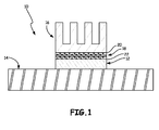
Figure 1 is a cross-sectional schematic view of an electronic device assembly of the present invention; -
Figure 2 is an isolation cross-sectional view of a thermally conductive dielectric interface of the present invention; -
Figure 3 is an isolation cross-sectional view of a thermally conductive dielectric interface of the present invention; -
Figure 4 is a performance comparison chart of a thermally conductive dielectric interface of the present invention; -
Figure 5 is a performance comparison chart of a thermally conductive dielectric interface of the present invention; and -
Figure 6 is a performance comparison chart of a thermally conductive dielectric interface of the present invention. - The objects, features, and advances represented by the present invention will now be presented in terms of detailed embodiments. Other embodiments and aspects of the invention are recognized as being within the grasp of those having ordinary skill in the art.
- Unless otherwise apparent or stated, directional references, such as "upper", "lower", "front", "rear", "vertical", "horizontal", "top", "bottom" and the like are intended to be relative to the orientation of a particular embodiment of the invention as shown in the figures. In addition, a given reference numeral in the drawings indicates the same or similar structure when it appears in different figures, and like reference numerals identify similar structural elements and/or features of the subject invention.
- With reference now to the drawing figures, an
electronic device assembly 10 includes a heat-generatingelectronic component 12 supported on asubstrate 14, which may typically be a printed circuit board (PCB).Electronic component 12 may be any of a variety of heat-generating devices commonly employed in electronics, such as a microprocessor, transistor, integrated microchip, or other power semiconductor device, etc.Electronic component 12 may be secured tosubstrate 14 through known means, such as soldering, pins, or other connections. The operation ofelectronic component 12 generates thermal energy, which is desirably dissipated away fromelectronic component 12 for optimal performance. To aid in dissipating excess thermal energy fromelectronic component 12,electronic device assembly 10 includes a thermal dissipation member orheat sink 16. In an example embodiment,thermal dissipation member 16 may be provided as a finned heat sink or other heat spreading structure as is commonly employed in the art. - A thermally conductive
dielectric interface 18 of the invention may be interposed between respectiveheat transfer surfaces thermal dissipation member 16 andelectronic component 12 to efficiently transport thermal energy therebetween.Interface 18 may preferably conform toheat transfer surfaces interface 18 andheat transfer surfaces Interface 18 preferably also provides a joint that both physically and thermally couplesthermal dissipation member 16 toelectronic component 12. It is to be understood, however, thatinterface 18 may not directly connectthermal dissipation member 16 toelectronic component 12, and may instead merely provide a thermally conductive joint along a thermal pathway between the heat-generatingelectronic component 12 andthermal dissipation member 16. - An isolation cross-sectional view of thermally conductive
dielectric interface 18 is illustrated inFigure 2 , including abase 30 having first andsecond sides upcoat 36 disposed at first andsecond sides base 30. A thickness "T" is defined alongthickness axis 38, which may be substantially perpendicular to first andsecond sides base 30. As illustrated inFigure 2 , interface thickness "T" extends throughupcoat 36 andbase 30. The thickness "T" ofinterface 18 is intended to represent the dimension between respectiveheat transfer surfaces thermal dissipation member 16 andelectronic component 12. In some embodiments, thickness "T" is between 100-600 micrometers (µm), whereinbase 30 may have an example thickness dimension "t1" of between 50-350 µm, andupcoat 36 may have a total thickness dimension ("t2A" + "t2B") of between 50-300 µm. To provide the benefits described herein, each upcoat layer thickness dimension "t2A" and "t2B" is preferably at least 25 µm, and more preferably between 50-150 µm. - A combination of materials, material thicknesses, and material conditions provide the desired set of characteristics of
interface 18 of the present invention. Among the desired properties ofinterface 18 are the conformability ofupcoat 36, the adhesion capabilities ofupcoat 36, a relatively lowcompressive modulus upcoat 36, a relatively high compressive modulus ofbase 30, a high dielectric voltage breakdown strength (also known as voltage breakdown) across thickness "T", and a high thermal conductivity across thickness "T". As an efficient thermal pathway betweenelectronic component 12 andthermal dissipation member 16,interface 18 preferably exhibits a thermal conductivity of at least 0.5 W/m *K through thickness "T", and may, in some embodiments, be between 0.5-3 W/m * K. Moreover,interface 18 is dielectric, and exhibits a voltage breakdown of at least 3 kV. - To accomplish the properties described above,
interface 18 may be installed intoassembly 10 in an intermediate condition with a relatively "hard"base 30 and a relatively "soft"upcoat 36, with one or more ofbase 30 andupcoat 36 being suitably thermally conductive and electrically insulative. In this intermediate condition,base 30 exhibits a compressive modulus of at least 105 Pa (100,000 Pa), andupcoat 36 exhibits a compressive modulus of less than 104 Pa (10,000 Pa). For the purposes hereof, the term "compressive modulus" is intended to mean a modulus of elasticity (Young's Modulus), and is the ratio of stress to strain, with units of pressure. In the final finished condition ofelectronic device assembly 10,upcoat 36 may have a compressive modulus exceeding 104 Pa. - One aspect of the present invention is to obtain a thermally conductive, dielectric interface that exhibits a desired voltage breakdown value, as tested by ASTM D149. The present arrangement achieves the desired voltage breakdown with the relatively high
compressive modulus base 30 that is sufficiently rigid to preventinterface 18 from excessively compressing alongthickness axis 38 when mounted inelectronic device assembly 10. Many conventional conformable thermal interfaces excessively compress along their respective thickness axis, such that the gap between components, such as between an electrical component and a thermal dissipation member, can become small enough to cause voltage breakdown. Moreover, if a heat transfer surface of one of the components in the electronic device assembly has an irregular or burred surface, penetration through an excessively "soft" material can lead to an electrical short or premature voltage breakdown of the thermal interface. - A variety of materials are contemplated as being useful in the production of
interface 18, with the overall goal being to obtain a core 30 with a compressive modulus of at least 105 Pa, an upcoat with a compressive modulus, in an intermediate condition, of less than 104 Pa, and with the interface exhibiting a voltage breakdown of at least 3 kV, and a thermal conductivity of at least 0.5 W/m * K through thickness "T". In some embodiments,interface 18 may exhibit an electrical resistance of at least 1010 Ω * m through thickness "T". In one embodiment,base 30 includes a vinyl silicone polymer matrix within which is dispersed thermally conductive particulate filler, such as alumina. Upcoat may include a vinyl and hydride-functional silicone polymer matrix within which is dispersed a thermally conductive particulate filler, such as alumina. - Both of
base 30 andupcoat 36 may preferably be formed of a thermoplastic or thermosetting polymer matrix loaded with thermally conductive particulate material. Example thermoplastic and thermosetting resins useful in the polymeric matrix ofbase 30 andupcoat 36 include silicone, acrylic, urethane, epoxy, polysulfide, polyisobutylene, and polyvinyl or polyolefin based polymers. The desired compressive moduli ofbase 30 andupcoat 36 may be achieved through one or more of polymer matrix material selection, cross-linking agent selection, cross-linking controls, cure extent, and the like. - Thermally conductive particulate filler is well known in the art for enhancing the thermal conductivity of a polymer matrix. Example thermally conductive fillers useful in the polymer matrices of the present invention include metals or ceramics, and specifically include, for example, alumina, aluminum nitride, aluminum hydroxide, aluminum oxide, boron nitride, zinc nitride, and silicon carbide. The thermally conductive particulate filler may be dispersed within the polymer matrices at a loading concentration of between about 5-90% by volume, to achieve a desired minimum thermal conductivity through thickness "T" of 0.5 W/m * K. In some embodiments, both of
base 30 andupcoat 36 exhibit thermal conductivities of at least 0.5 W/m * K, though it is contemplated that, in other embodiments, only one ofbase 30 andupcoat 36 exhibit a thermal conductivity of at least 0.5 W/m * K, but nevertheless resulting in aninterface 18 exhibiting a thermal conductivity of at least 0.5 W/m * K through thickness "T". - Another embodiment of the present invention is illustrated in
Figure 3 , wherein thermally conductivedielectric interface 118 includes acore 128 having first and second opposed surfaces 129A, 129B defining respective first andsecond sides interface 118. Abase layer 130 includes aninner surface 132 that is applied to each of first and second surfaces 129A, 129B ofcore 128. In this embodiment,core 128 acts as a substrate upon whichbase layer 130 may be applied. In one embodiment,core 128 may be a flexible fiberglass film.Core 128 may not, in some embodiments, appreciably affect the performance properties ofinterface 118, and may instead primarily serve as a substrate upon which to build the laminate structure ofinterface 118. Accordingly,core 128 preferably does not significantly inhibit thermal transmission through thickness "T" ofinterface 118, nor doescore 128 significantly detrimentally affect the electrical resistance and voltage breakdown characteristics ofinterface 118.Core 128 may therefore be selected from a variety of materials and configurations as deemed necessary per application. In some embodiments,core 128 may itself exhibit a thermal conductivity of at least 0.5 W/m * K, though it is to be understood that such thermal conductivity characteristic is not required ofcore 128. In some embodiments,core 128 may include thermally conductive particulate material dispersed therein to enhance the thermal conductivity ofcore 128. -
Base layer 130 ofinterface 118 may be analogous tobase 30 ofinterface 18, but withcore 128 disposed at least partially within the base. Accordingly,base layer 130 may be, in effect, a base 30 applied to first and second surfaces 129A, 129B ofcore 128.Base layer 130 may preferably be a polymer matrix that exhibits a compressive modulus of at least 105 Pa, and may include thermally conductive particles dispersed therein to enhance its thermal conductivity properties. The composition ofbase layer 130 may, in some embodiments, be analogous to that described above with respect tobase 30 ofinterface 18. For example,base layer 130 may include a silicone polymer preparation in which thermally conductive particles are dispersed. -
Interface 118 further includes anupcoat layer 136 applied toouter surface 134 ofbase layer 130 at both first andsecond sides interface 118. In preferred embodiments,upcoat layer 136 may be analogous to upcoat 36 ofinterface 18, as described above.Upcoat layer 136 may comprise a polymer matrix, and exhibit, in an intermediate condition, a compressive modulus of less than 104 Pa. In some embodiments,upcoat layer 136 may include a silicone polymer preparation in which thermally conductive particles are dispersed to enhance thermal conductivity properties thereof.Upcoat layer 136 may exhibit a compressive modulus exceeding 104 Pa in its finished condition, such as inelectronic assembly 10. -
Interface 118 may include first andsecond release liners interface 18 prior to the production of electronic device assembly 10 (such as whenupcoat layer 136 is still in its intermediate condition). First andsecond release liners interface 118 atelectronic device assembly 10. Consequently, a thickness "T" ofinterface 118 does not includerelease liners such liners interface 118 inelectronic device assembly 10. Thickness "T" ofinterface 118 is defined alongthickness axis 138, and extends throughupcoat layer 136,base layer 130, andcore 128. Interface 118 exhibits a thermal conductivity of at least 0.5 W/m * K, and an electrical resistance of at least 1010 Ω * m through thickness "T". Moreover,interface 118 preferably exhibits a voltage breakdown value of at least 3 kV through thickness "T". - As described above,
interface 118 not only provides an efficient pathway for transfer of thermal energy, but may also act as a joint for securing together separate components of an assembly, such aselectronic device assembly 10. The interfaces of the present invention therefore further exhibit adhesion properties for establishing a strong bond to such components. The interfaces of the present invention may be prepared through a variety of known techniques. An example preparation technique includes solventcoating base layer 130 at 60-70% solids by weight to first andsecond sides core 128 to a substrate thickness "t3" of between about 100-250 µm, which includes the thickness ofbase layer 130 andcore layer 128.Base layer 130 may then be dried of solvent and cross-linked (cured) in a forced-air oven to achieve a compressive modulus of at least 105 Pa.Upcoat layer 136 may then be solvent coated at at 60-70% solids by weightouter surface 134 ofbase layer 130 to a total thickness "T" of between 150-600 µm.Upcoat layer 136 may be dried of solvent, but otherwise left substantially as-is (uncured) with a compressive modulus of less than 104 Pa in the intermediate condition ofupcoat layer 136. Due to the general tackiness of the relatively low-modulusuncured upcoat layer 136,release liners upcoat layer 136 to facilitate handling ofinterface 118 prior to installation in an electronic device assembly. At installation, one or both ofrelease liners upcoat layer 136 to expose the relatively low modulus (< 104 Pa)uncured upcoat layer 136. The interface may then be positioned for attachment to, for example, one or more ofthermal dissipation member 16 andelectronic component 12, withupcoat layer 136 in contact with respective heat transfer surfaces of suchthermal dissipation member 16 andelectronic component 12. A force may be applied to ensure securing contact as betweeninterface 118 and the respective components ofelectronic device assembly 10, followed by a curing procedure to cause cross-linking inupcoat layer 136, with such cross-linking (curing) enhancing the adhesion/bonding of the components to the interface, and bringingupcoat layer 136 to a finished condition. Typical assembly pressure applied in the securing process may be between about 75-300 psi. Such pressure may be applied for a predetermined period of time prior to the curing process forupcoat layer 136, or may be applied at constant or varying levels throughout theupcoat layer 136 curing process. In one embodiment, upcoat layer 136 (and upcoat 36) cures to its finished condition upon six minutes in an oven set at 160°C. It is to be understood, however, that various curing modalities and procedures may be employed to appropriately cure the base and upcoat layers of the present interfaces. - An interface in accordance with the structure illustrated in
Figure 3 was prepared with a thickness "T" of 250 µm ("Example 1"), and compared to a conventional interface available from Arlon, LLC of Bear, Delaware under the trade name Secure® 1500 FG ("Comparison Sample"). The following table sets forth the comparison results, with the bonding data representing the application of a TO-220 transistor electronic component coupled to a solid aluminum base via the respective interface with the stated application pressure:Table 1 Material Initial Bonding Pressure (psi) Initial Bonding Time (s) Failure Torque (in-lb) Voltage Breakdown (kVAC) Thermal Performance (°C/W) Example 1 300 10 27.2 5.28 1.98 Comparison Sample 300 10 18.5 4.42 1.98 Example 1 300 30 32.3 5.46 2.04 Comparison Sample 300 30 21.1 4.18 1.98 Example 1 300 300 31.7 5.22 2.07 Comparison Sample 300 300 17.3 3.53 2.1 Example 1 300 900 30.7 4.82 2.02 Comparison Sample 300 900 16.2 1.3 2.1 -
Figures 4-6 represent the performance characteristics of the present interface in comparison to the Arlon Secure® 1500 FG material under a 300 psi assembly pressure for up to 900 seconds.Figures 4-6 clearly demonstrate an improved voltage breakdown, particularly with increasing assembly time, as well as significantly improved adhesion characteristics, without diminishing thermal perfomance. The performance data represented inFigures 4-6 was obtained through testing following the cure of the upcoat layer of the present interface to its finished condition, wherein the upcoat layer may exhibit a compressive modulus exceeding 104 Pa. - The invention has been described herein in considerable detail in order to comply with the patent statutes, and to provide those skilled in the art with the information needed to apply the novel principles and to construct and use embodiments of the invention as required. However, it is to be understood that various modifications can be accomplished without departing from the scope of the invention itself.
Claims (14)
- A thermally conductive dielectric interface, comprising:a base having first and second sides substantially parallel to a base plane, and exhibiting a compressive modulus of at least 105 Pa, said base comprising a first silicone polymer preparation; andan upcoat disposed at said first and second sides of said base, said upcoat exhibiting a compressive modulus of less than 104 Pa, and comprising a second silicone polymer preparation, wherein a thickness of said interface is defined along an axis perpendicular to said base plane and extends through said upcoat and said base, and said interface exhibiting a voltage breakdown value of at least 3 kV and a thermal conductivity of at least 0.5 W/m * K through said thickness.
- A thermally conductive dielectric interface as in Claim 1, including particulate filler dispersed in each of said first and second silicone polymer preparations.
- A thermally conductive dielectric interface as in any of Claims 1 and 2 wherein said first silicone polymer preparation is more fully cured than said second silicone polymer preparation.
- A thermally conductive dielectric interface as in any preceding claim wherein said interface exhibits an electrical resistance of at least 1010 Ω * m through said thickness.
- A thermally conductive dielectric interface as in any preceding claim wherein said base is between 0.1-0.25 mm along said axis.
- A thermally conductive dielectric interface as in Claim 5 wherein said upcoat is between 0.05-0.30 mm along said axis.
- A method for mounting a heat sink to a heat-generating component, said method comprising securing the thermally conductive dielectric interface of any preceding claim between said heat sink and said heat-generating component.
- A method as in Claim 7 wherein said upcoat bonds said interface to said heat sink and said heat-generating component.
- A method as in Claim 8, including, subsequent to bonding said interface to said heat sink and said heat-generating component, curing said upcoat to an extent at which said upcoat exhibits a compressive modulus of greater than 104 Pa.
- A method as in Claim 9 wherein said curing includes initiating a cross-linking reaction in said second silicone polymer preparation
- A thermally conductive dielectric interface, comprising:a core having first and second opposed surfaces substantially parallel to a core plane, and defining respective first and second sides of said interface;a base layer with an inner surface applied to each of said first and second surfaces of said core, said base layer comprising thermally conductive particles dispersed in a first polymer preparation, wherein said base layer exhibits a compressive modulus of at least 105 Pa; andan upcoat layer applied to an outer surface of said base layer at both said first and second sides of said interface, said upcoat layer comprising thermally conductive particles dispersed in a second polymer preparation, wherein said upcoat layer exhibits a compressive modulus of less than 104 Pa,wherein a thickness of said thermally conductive interface is defined along an axis perpendicular to said core plane and extends through said upcoat layer, said base layer, and said core, and said interface exhibits a thermal conductivity of at least 0.5 W/m * K, and an electrical resistance of at least 1010 Ω * m through said thickness.
- A thermally conductive dielectric interface as in Claim 11, wherein said thermally conductive particles are metal or ceramic.
- A thermally conductive interface as in any of Claims 11 and 12 wherein said core comprises a fiberglass film.
- A thermally conductive interface as in any of Claims 11 to 13 wherein said first and second polymer preparations include a silicone polymer matrix.
Applications Claiming Priority (2)
| Application Number | Priority Date | Filing Date | Title |
|---|---|---|---|
| US201361839116P | 2013-06-25 | 2013-06-25 | |
| US14/310,231 US9693481B2 (en) | 2013-06-25 | 2014-06-20 | Thermally conductive dielectric interface |
Publications (3)
| Publication Number | Publication Date |
|---|---|
| EP2819158A2 true EP2819158A2 (en) | 2014-12-31 |
| EP2819158A3 EP2819158A3 (en) | 2015-04-22 |
| EP2819158B1 EP2819158B1 (en) | 2019-09-11 |
Family
ID=51063274
Family Applications (1)
| Application Number | Title | Priority Date | Filing Date |
|---|---|---|---|
| EP14173731.2A Active EP2819158B1 (en) | 2013-06-25 | 2014-06-24 | Thermally conductive dielectric interface |
Country Status (4)
| Country | Link |
|---|---|
| US (1) | US9693481B2 (en) |
| EP (1) | EP2819158B1 (en) |
| KR (3) | KR101682761B1 (en) |
| CN (1) | CN104254229B (en) |
Cited By (2)
| Publication number | Priority date | Publication date | Assignee | Title |
|---|---|---|---|---|
| US10870749B2 (en) | 2017-07-05 | 2020-12-22 | The University Of Akron | Thermally conductive polymers and methods for making |
| WO2023001637A1 (en) * | 2021-07-22 | 2023-01-26 | Kostal Automobil Elektrik Gmbh & Co. Kg | Assembly for cooling a high-voltage part |
Families Citing this family (12)
| Publication number | Priority date | Publication date | Assignee | Title |
|---|---|---|---|---|
| KR102340828B1 (en) * | 2014-10-23 | 2021-12-17 | 삼성전자주식회사 | Printed circuit board assembly manufacturing method |
| WO2017044712A1 (en) | 2015-09-11 | 2017-03-16 | Laird Technologies, Inc. | Devices for absorbing energy from electronic components |
| DE102015118245B4 (en) * | 2015-10-26 | 2024-10-10 | Infineon Technologies Austria Ag | Electronic component with a thermal interface material, manufacturing method for an electronic component, heat dissipation body with a thermal interface material and thermal interface material |
| US11335621B2 (en) * | 2016-07-19 | 2022-05-17 | International Business Machines Corporation | Composite thermal interface objects |
| JP7160101B2 (en) * | 2018-08-23 | 2022-10-25 | 昭和電工マテリアルズ株式会社 | Method for manufacturing semiconductor device, heat conductive sheet, and method for manufacturing heat conductive sheet |
| US11482467B2 (en) * | 2018-08-23 | 2022-10-25 | Showa Denko Materials Co., Ltd. | Thermally conductive sheet and method of manufacturing semiconductor device |
| CN112689927B (en) * | 2018-09-18 | 2023-01-10 | 京瓷Avx元器件公司 | filter components |
| TWI841603B (en) * | 2018-09-27 | 2024-05-11 | 德商漢高股份有限及兩合公司 | Abrasion-resistant coatings for thermal interfaces |
| TW202543812A (en) | 2019-10-25 | 2025-11-16 | 德商漢高股份有限及兩合公司 | Three-dimensionally patternable thermal interface |
| KR102172003B1 (en) | 2019-11-28 | 2020-11-02 | (주)매그나텍 | Method for manufacturing substitute substrate for adhesive |
| US11705676B2 (en) * | 2020-12-11 | 2023-07-18 | Caterpillar Inc. | Method and apparatus for tracking a life cycle of turbocharger |
| WO2025222197A1 (en) * | 2024-04-19 | 2025-10-23 | Henkel Ag & Co. Kgaa | Thermally conductive dielectric interface |
Citations (1)
| Publication number | Priority date | Publication date | Assignee | Title |
|---|---|---|---|---|
| US4810563A (en) | 1986-03-14 | 1989-03-07 | The Bergquist Company | Thermally conductive, electrically insulative laminate |
Family Cites Families (21)
| Publication number | Priority date | Publication date | Assignee | Title |
|---|---|---|---|---|
| TW422874B (en) | 1996-10-08 | 2001-02-21 | Hitachi Chemical Co Ltd | Semiconductor device, semiconductor chip mounting substrate, methods of manufacturing the device and substrate, adhesive, and adhesive double coated film |
| JP4161544B2 (en) | 1996-10-08 | 2008-10-08 | 日立化成工業株式会社 | Adhesive film for mounting semiconductor elements |
| US6432497B2 (en) | 1997-07-28 | 2002-08-13 | Parker-Hannifin Corporation | Double-side thermally conductive adhesive tape for plastic-packaged electronic components |
| US6706219B2 (en) | 1999-09-17 | 2004-03-16 | Honeywell International Inc. | Interface materials and methods of production and use thereof |
| US6605238B2 (en) | 1999-09-17 | 2003-08-12 | Honeywell International Inc. | Compliant and crosslinkable thermal interface materials |
| JP3468420B2 (en) | 2000-06-07 | 2003-11-17 | 持田商工株式会社 | Heat radiating sheet and method of manufacturing the same |
| US6822018B2 (en) * | 2002-02-15 | 2004-11-23 | Delphi Technologies, Inc. | Thermally-conductive electrically-insulating polymer-base material |
| US6657297B1 (en) | 2002-08-15 | 2003-12-02 | The Bergquist Company | Flexible surface layer film for delivery of highly filled or low cross-linked thermally conductive interface pads |
| JP2004134604A (en) | 2002-10-11 | 2004-04-30 | Shin Etsu Chem Co Ltd | Electromagnetic wave absorbing heat conductive sheet |
| US6783692B2 (en) * | 2002-10-17 | 2004-08-31 | Dow Corning Corporation | Heat softening thermally conductive compositions and methods for their preparation |
| US6956739B2 (en) | 2002-10-29 | 2005-10-18 | Parker-Hannifin Corporation | High temperature stable thermal interface material |
| US8119191B2 (en) | 2003-01-16 | 2012-02-21 | Parker-Hannifin Corporation | Dispensable cured resin |
| US7229683B2 (en) | 2003-05-30 | 2007-06-12 | 3M Innovative Properties Company | Thermal interface materials and method of making thermal interface materials |
| US7655719B2 (en) * | 2004-07-13 | 2010-02-02 | Cool Options, Inc. | Thermally conductive polymer compositions having moderate tensile and flexural properties |
| US20060228542A1 (en) * | 2005-04-08 | 2006-10-12 | Saint-Gobain Performance Plastics Corporation | Thermal interface material having spheroidal particulate filler |
| US8263250B2 (en) | 2007-06-18 | 2012-09-11 | Tesla Motors, Inc. | Liquid cooling manifold with multi-function thermal interface |
| KR101174971B1 (en) | 2007-09-05 | 2012-08-17 | 세키스이가가쿠 고교가부시키가이샤 | Insulating sheet and multilayer structure |
| US8081468B2 (en) | 2009-06-17 | 2011-12-20 | Laird Technologies, Inc. | Memory modules including compliant multilayered thermally-conductive interface assemblies |
| WO2012046814A1 (en) | 2010-10-06 | 2012-04-12 | 日立化成工業株式会社 | Multilayer resin sheet and process for production thereof, resin sheet laminate and process for production thereof, cured multilayer resin sheet, metal-foil-cladded multilayer resin sheet, and semiconductor device |
| EP2692526B1 (en) | 2011-03-28 | 2020-10-28 | Hitachi Chemical Company, Ltd. | Multilayer resin sheet, resin sheet laminate, cured multilayer resin sheet and method for producing same, multilayer resin sheet with metal foil, and semiconductor device |
| KR101204718B1 (en) * | 2012-05-02 | 2012-11-26 | 김선기 | Thermal conductive plate member having improved thermal conductivity |
-
2014
- 2014-06-20 US US14/310,231 patent/US9693481B2/en active Active
- 2014-06-24 EP EP14173731.2A patent/EP2819158B1/en active Active
- 2014-06-24 KR KR1020140076938A patent/KR101682761B1/en active Active
- 2014-06-25 CN CN201410289683.7A patent/CN104254229B/en active Active
-
2016
- 2016-07-21 KR KR1020160092802A patent/KR102264624B1/en active Active
-
2020
- 2020-04-16 KR KR1020200045982A patent/KR20200043949A/en not_active Ceased
Patent Citations (1)
| Publication number | Priority date | Publication date | Assignee | Title |
|---|---|---|---|---|
| US4810563A (en) | 1986-03-14 | 1989-03-07 | The Bergquist Company | Thermally conductive, electrically insulative laminate |
Cited By (2)
| Publication number | Priority date | Publication date | Assignee | Title |
|---|---|---|---|---|
| US10870749B2 (en) | 2017-07-05 | 2020-12-22 | The University Of Akron | Thermally conductive polymers and methods for making |
| WO2023001637A1 (en) * | 2021-07-22 | 2023-01-26 | Kostal Automobil Elektrik Gmbh & Co. Kg | Assembly for cooling a high-voltage part |
Also Published As
| Publication number | Publication date |
|---|---|
| KR101682761B1 (en) | 2016-12-05 |
| KR102264624B1 (en) | 2021-06-15 |
| KR20200043949A (en) | 2020-04-28 |
| EP2819158A3 (en) | 2015-04-22 |
| CN104254229A (en) | 2014-12-31 |
| KR20150002485A (en) | 2015-01-07 |
| EP2819158B1 (en) | 2019-09-11 |
| US20140374071A1 (en) | 2014-12-25 |
| KR20160091859A (en) | 2016-08-03 |
| US9693481B2 (en) | 2017-06-27 |
| CN104254229B (en) | 2017-08-08 |
Similar Documents
| Publication | Publication Date | Title |
|---|---|---|
| EP2819158B1 (en) | Thermally conductive dielectric interface | |
| CN107039289B (en) | Thermal bonding materials with defined thermal, mechanical and electrical properties | |
| CN101325186B (en) | Insulating sheet and method for producing it, and power module comprising the insulating sheet | |
| JP3209132B2 (en) | Metal base substrate | |
| CN1206892C (en) | Method of applying phase change thermal interface material | |
| JP4089636B2 (en) | Method for manufacturing thermally conductive resin sheet and method for manufacturing power module | |
| CN1255868C (en) | Connecting materials | |
| JP3559137B2 (en) | Heat conductive adhesive composition and heat conductive adhesive film using the composition | |
| CN1720108A (en) | Thermally conductive EMI shielding | |
| CN1879009A (en) | Air-gap insulators for short-term exposure to high ambient temperatures | |
| JP5509461B2 (en) | Power semiconductor device and manufacturing method thereof | |
| KR102829764B1 (en) | Thermal management of high-temperature flux multi-component assemblies | |
| JP2010245563A (en) | Parts unit | |
| JP2003193016A (en) | Highly thermo resistant adhesive film with high heat dissipation | |
| JP4111187B2 (en) | Manufacturing method of component unit | |
| JP2003309235A (en) | Heat dissipation member and power module | |
| JP2017149909A (en) | Thermally conductive adhesive composition, thermal conductive adhesive sheet and method for producing laminate | |
| JP2006156721A5 (en) | ||
| CN205258365U (en) | Heat conduction electrical insulator | |
| JP4581655B2 (en) | Heat sink | |
| JP4013945B2 (en) | Manufacturing method of component unit | |
| KR20210003352A (en) | Fod adhesive film and semiconductor package comprising thereof | |
| KR100515747B1 (en) | Heat-resistance adhesive tape for electronic components | |
| CN1247724C (en) | Adhesive and electric device | |
| JP2000178517A (en) | Thermosetting adhesive sheet |
Legal Events
| Date | Code | Title | Description |
|---|---|---|---|
| PUAI | Public reference made under article 153(3) epc to a published international application that has entered the european phase |
Free format text: ORIGINAL CODE: 0009012 |
|
| 17P | Request for examination filed |
Effective date: 20140624 |
|
| AK | Designated contracting states |
Kind code of ref document: A2 Designated state(s): AL AT BE BG CH CY CZ DE DK EE ES FI FR GB GR HR HU IE IS IT LI LT LU LV MC MK MT NL NO PL PT RO RS SE SI SK SM TR |
|
| AX | Request for extension of the european patent |
Extension state: BA ME |
|
| PUAL | Search report despatched |
Free format text: ORIGINAL CODE: 0009013 |
|
| AK | Designated contracting states |
Kind code of ref document: A3 Designated state(s): AL AT BE BG CH CY CZ DE DK EE ES FI FR GB GR HR HU IE IS IT LI LT LU LV MC MK MT NL NO PL PT RO RS SE SI SK SM TR |
|
| AX | Request for extension of the european patent |
Extension state: BA ME |
|
| RIC1 | Information provided on ipc code assigned before grant |
Ipc: H01L 23/42 20060101ALI20150319BHEP Ipc: H01L 23/373 20060101AFI20150319BHEP Ipc: H05K 7/20 20060101ALI20150319BHEP Ipc: B23P 15/26 20060101ALI20150319BHEP |
|
| RAP1 | Party data changed (applicant data changed or rights of an application transferred) |
Owner name: HENKEL IP & HOLDING GMBH |
|
| R17P | Request for examination filed (corrected) |
Effective date: 20151008 |
|
| RBV | Designated contracting states (corrected) |
Designated state(s): AL AT BE BG CH CY CZ DE DK EE ES FI FR GB GR HR HU IE IS IT LI LT LU LV MC MK MT NL NO PL PT RO RS SE SI SK SM TR |
|
| 17Q | First examination report despatched |
Effective date: 20161017 |
|
| STAA | Information on the status of an ep patent application or granted ep patent |
Free format text: STATUS: EXAMINATION IS IN PROGRESS |
|
| GRAP | Despatch of communication of intention to grant a patent |
Free format text: ORIGINAL CODE: EPIDOSNIGR1 |
|
| STAA | Information on the status of an ep patent application or granted ep patent |
Free format text: STATUS: GRANT OF PATENT IS INTENDED |
|
| INTG | Intention to grant announced |
Effective date: 20190528 |
|
| GRAS | Grant fee paid |
Free format text: ORIGINAL CODE: EPIDOSNIGR3 |
|
| GRAA | (expected) grant |
Free format text: ORIGINAL CODE: 0009210 |
|
| STAA | Information on the status of an ep patent application or granted ep patent |
Free format text: STATUS: THE PATENT HAS BEEN GRANTED |
|
| AK | Designated contracting states |
Kind code of ref document: B1 Designated state(s): AL AT BE BG CH CY CZ DE DK EE ES FI FR GB GR HR HU IE IS IT LI LT LU LV MC MK MT NL NO PL PT RO RS SE SI SK SM TR |
|
| REG | Reference to a national code |
Ref country code: GB Ref legal event code: FG4D |
|
| REG | Reference to a national code |
Ref country code: CH Ref legal event code: EP |
|
| REG | Reference to a national code |
Ref country code: AT Ref legal event code: REF Ref document number: 1179576 Country of ref document: AT Kind code of ref document: T Effective date: 20190915 |
|
| REG | Reference to a national code |
Ref country code: DE Ref legal event code: R096 Ref document number: 602014053313 Country of ref document: DE Ref country code: IE Ref legal event code: FG4D |
|
| REG | Reference to a national code |
Ref country code: NL Ref legal event code: MP Effective date: 20190911 |
|
| REG | Reference to a national code |
Ref country code: LT Ref legal event code: MG4D |
|
| PG25 | Lapsed in a contracting state [announced via postgrant information from national office to epo] |
Ref country code: NO Free format text: LAPSE BECAUSE OF FAILURE TO SUBMIT A TRANSLATION OF THE DESCRIPTION OR TO PAY THE FEE WITHIN THE PRESCRIBED TIME-LIMIT Effective date: 20191211 Ref country code: SE Free format text: LAPSE BECAUSE OF FAILURE TO SUBMIT A TRANSLATION OF THE DESCRIPTION OR TO PAY THE FEE WITHIN THE PRESCRIBED TIME-LIMIT Effective date: 20190911 Ref country code: HR Free format text: LAPSE BECAUSE OF FAILURE TO SUBMIT A TRANSLATION OF THE DESCRIPTION OR TO PAY THE FEE WITHIN THE PRESCRIBED TIME-LIMIT Effective date: 20190911 Ref country code: LT Free format text: LAPSE BECAUSE OF FAILURE TO SUBMIT A TRANSLATION OF THE DESCRIPTION OR TO PAY THE FEE WITHIN THE PRESCRIBED TIME-LIMIT Effective date: 20190911 Ref country code: FI Free format text: LAPSE BECAUSE OF FAILURE TO SUBMIT A TRANSLATION OF THE DESCRIPTION OR TO PAY THE FEE WITHIN THE PRESCRIBED TIME-LIMIT Effective date: 20190911 Ref country code: BG Free format text: LAPSE BECAUSE OF FAILURE TO SUBMIT A TRANSLATION OF THE DESCRIPTION OR TO PAY THE FEE WITHIN THE PRESCRIBED TIME-LIMIT Effective date: 20191211 |
|
| PG25 | Lapsed in a contracting state [announced via postgrant information from national office to epo] |
Ref country code: AL Free format text: LAPSE BECAUSE OF FAILURE TO SUBMIT A TRANSLATION OF THE DESCRIPTION OR TO PAY THE FEE WITHIN THE PRESCRIBED TIME-LIMIT Effective date: 20190911 Ref country code: LV Free format text: LAPSE BECAUSE OF FAILURE TO SUBMIT A TRANSLATION OF THE DESCRIPTION OR TO PAY THE FEE WITHIN THE PRESCRIBED TIME-LIMIT Effective date: 20190911 Ref country code: ES Free format text: LAPSE BECAUSE OF FAILURE TO SUBMIT A TRANSLATION OF THE DESCRIPTION OR TO PAY THE FEE WITHIN THE PRESCRIBED TIME-LIMIT Effective date: 20190911 Ref country code: GR Free format text: LAPSE BECAUSE OF FAILURE TO SUBMIT A TRANSLATION OF THE DESCRIPTION OR TO PAY THE FEE WITHIN THE PRESCRIBED TIME-LIMIT Effective date: 20191212 Ref country code: RS Free format text: LAPSE BECAUSE OF FAILURE TO SUBMIT A TRANSLATION OF THE DESCRIPTION OR TO PAY THE FEE WITHIN THE PRESCRIBED TIME-LIMIT Effective date: 20190911 |
|
| PG25 | Lapsed in a contracting state [announced via postgrant information from national office to epo] |
Ref country code: PT Free format text: LAPSE BECAUSE OF FAILURE TO SUBMIT A TRANSLATION OF THE DESCRIPTION OR TO PAY THE FEE WITHIN THE PRESCRIBED TIME-LIMIT Effective date: 20200113 Ref country code: RO Free format text: LAPSE BECAUSE OF FAILURE TO SUBMIT A TRANSLATION OF THE DESCRIPTION OR TO PAY THE FEE WITHIN THE PRESCRIBED TIME-LIMIT Effective date: 20190911 Ref country code: NL Free format text: LAPSE BECAUSE OF FAILURE TO SUBMIT A TRANSLATION OF THE DESCRIPTION OR TO PAY THE FEE WITHIN THE PRESCRIBED TIME-LIMIT Effective date: 20190911 Ref country code: PL Free format text: LAPSE BECAUSE OF FAILURE TO SUBMIT A TRANSLATION OF THE DESCRIPTION OR TO PAY THE FEE WITHIN THE PRESCRIBED TIME-LIMIT Effective date: 20190911 Ref country code: EE Free format text: LAPSE BECAUSE OF FAILURE TO SUBMIT A TRANSLATION OF THE DESCRIPTION OR TO PAY THE FEE WITHIN THE PRESCRIBED TIME-LIMIT Effective date: 20190911 |
|
| PG25 | Lapsed in a contracting state [announced via postgrant information from national office to epo] |
Ref country code: IS Free format text: LAPSE BECAUSE OF FAILURE TO SUBMIT A TRANSLATION OF THE DESCRIPTION OR TO PAY THE FEE WITHIN THE PRESCRIBED TIME-LIMIT Effective date: 20200224 Ref country code: SM Free format text: LAPSE BECAUSE OF FAILURE TO SUBMIT A TRANSLATION OF THE DESCRIPTION OR TO PAY THE FEE WITHIN THE PRESCRIBED TIME-LIMIT Effective date: 20190911 Ref country code: SK Free format text: LAPSE BECAUSE OF FAILURE TO SUBMIT A TRANSLATION OF THE DESCRIPTION OR TO PAY THE FEE WITHIN THE PRESCRIBED TIME-LIMIT Effective date: 20190911 Ref country code: CZ Free format text: LAPSE BECAUSE OF FAILURE TO SUBMIT A TRANSLATION OF THE DESCRIPTION OR TO PAY THE FEE WITHIN THE PRESCRIBED TIME-LIMIT Effective date: 20190911 |
|
| REG | Reference to a national code |
Ref country code: DE Ref legal event code: R097 Ref document number: 602014053313 Country of ref document: DE |
|
| PLBE | No opposition filed within time limit |
Free format text: ORIGINAL CODE: 0009261 |
|
| STAA | Information on the status of an ep patent application or granted ep patent |
Free format text: STATUS: NO OPPOSITION FILED WITHIN TIME LIMIT |
|
| PG2D | Information on lapse in contracting state deleted |
Ref country code: IS |
|
| PG25 | Lapsed in a contracting state [announced via postgrant information from national office to epo] |
Ref country code: DK Free format text: LAPSE BECAUSE OF FAILURE TO SUBMIT A TRANSLATION OF THE DESCRIPTION OR TO PAY THE FEE WITHIN THE PRESCRIBED TIME-LIMIT Effective date: 20190911 Ref country code: IS Free format text: LAPSE BECAUSE OF FAILURE TO SUBMIT A TRANSLATION OF THE DESCRIPTION OR TO PAY THE FEE WITHIN THE PRESCRIBED TIME-LIMIT Effective date: 20200112 |
|
| 26N | No opposition filed |
Effective date: 20200615 |
|
| PG25 | Lapsed in a contracting state [announced via postgrant information from national office to epo] |
Ref country code: SI Free format text: LAPSE BECAUSE OF FAILURE TO SUBMIT A TRANSLATION OF THE DESCRIPTION OR TO PAY THE FEE WITHIN THE PRESCRIBED TIME-LIMIT Effective date: 20190911 |
|
| PG25 | Lapsed in a contracting state [announced via postgrant information from national office to epo] |
Ref country code: MC Free format text: LAPSE BECAUSE OF FAILURE TO SUBMIT A TRANSLATION OF THE DESCRIPTION OR TO PAY THE FEE WITHIN THE PRESCRIBED TIME-LIMIT Effective date: 20190911 |
|
| REG | Reference to a national code |
Ref country code: CH Ref legal event code: PL |
|
| PG25 | Lapsed in a contracting state [announced via postgrant information from national office to epo] |
Ref country code: LU Free format text: LAPSE BECAUSE OF NON-PAYMENT OF DUE FEES Effective date: 20200624 |
|
| REG | Reference to a national code |
Ref country code: BE Ref legal event code: MM Effective date: 20200630 |
|
| PG25 | Lapsed in a contracting state [announced via postgrant information from national office to epo] |
Ref country code: CH Free format text: LAPSE BECAUSE OF NON-PAYMENT OF DUE FEES Effective date: 20200630 Ref country code: LI Free format text: LAPSE BECAUSE OF NON-PAYMENT OF DUE FEES Effective date: 20200630 Ref country code: IE Free format text: LAPSE BECAUSE OF NON-PAYMENT OF DUE FEES Effective date: 20200624 |
|
| PG25 | Lapsed in a contracting state [announced via postgrant information from national office to epo] |
Ref country code: BE Free format text: LAPSE BECAUSE OF NON-PAYMENT OF DUE FEES Effective date: 20200630 |
|
| REG | Reference to a national code |
Ref country code: AT Ref legal event code: UEP Ref document number: 1179576 Country of ref document: AT Kind code of ref document: T Effective date: 20190911 |
|
| PG25 | Lapsed in a contracting state [announced via postgrant information from national office to epo] |
Ref country code: TR Free format text: LAPSE BECAUSE OF FAILURE TO SUBMIT A TRANSLATION OF THE DESCRIPTION OR TO PAY THE FEE WITHIN THE PRESCRIBED TIME-LIMIT Effective date: 20190911 Ref country code: MT Free format text: LAPSE BECAUSE OF FAILURE TO SUBMIT A TRANSLATION OF THE DESCRIPTION OR TO PAY THE FEE WITHIN THE PRESCRIBED TIME-LIMIT Effective date: 20190911 Ref country code: CY Free format text: LAPSE BECAUSE OF FAILURE TO SUBMIT A TRANSLATION OF THE DESCRIPTION OR TO PAY THE FEE WITHIN THE PRESCRIBED TIME-LIMIT Effective date: 20190911 |
|
| PG25 | Lapsed in a contracting state [announced via postgrant information from national office to epo] |
Ref country code: MK Free format text: LAPSE BECAUSE OF FAILURE TO SUBMIT A TRANSLATION OF THE DESCRIPTION OR TO PAY THE FEE WITHIN THE PRESCRIBED TIME-LIMIT Effective date: 20190911 |
|
| REG | Reference to a national code |
Ref country code: DE Ref legal event code: R081 Ref document number: 602014053313 Country of ref document: DE Owner name: HENKEL AG & CO. KGAA, DE Free format text: FORMER OWNER: HENKEL IP & HOLDING GMBH, 40589 DUESSELDORF, DE |
|
| REG | Reference to a national code |
Ref country code: GB Ref legal event code: 732E Free format text: REGISTERED BETWEEN 20220811 AND 20220817 |
|
| REG | Reference to a national code |
Ref country code: AT Ref legal event code: PC Ref document number: 1179576 Country of ref document: AT Kind code of ref document: T Owner name: HENKEL AG & CO. KGAA, DE Effective date: 20221003 |
|
| P01 | Opt-out of the competence of the unified patent court (upc) registered |
Effective date: 20230530 |
|
| PGFP | Annual fee paid to national office [announced via postgrant information from national office to epo] |
Ref country code: DE Payment date: 20250618 Year of fee payment: 12 |
|
| PGFP | Annual fee paid to national office [announced via postgrant information from national office to epo] |
Ref country code: GB Payment date: 20250618 Year of fee payment: 12 |
|
| PGFP | Annual fee paid to national office [announced via postgrant information from national office to epo] |
Ref country code: FR Payment date: 20250624 Year of fee payment: 12 |
|
| PGFP | Annual fee paid to national office [announced via postgrant information from national office to epo] |
Ref country code: AT Payment date: 20250620 Year of fee payment: 12 |
|
| PGFP | Annual fee paid to national office [announced via postgrant information from national office to epo] |
Ref country code: IT Payment date: 20250624 Year of fee payment: 12 |
|
| REG | Reference to a national code |
Ref country code: DE Ref legal event code: R079 Ref document number: 602014053313 Country of ref document: DE Free format text: PREVIOUS MAIN CLASS: H01L0023373000 Ipc: H10W0040250000 |