EP2817885B1 - High resolution pulse width modulator - Google Patents
High resolution pulse width modulator Download PDFInfo
- Publication number
- EP2817885B1 EP2817885B1 EP13707260.9A EP13707260A EP2817885B1 EP 2817885 B1 EP2817885 B1 EP 2817885B1 EP 13707260 A EP13707260 A EP 13707260A EP 2817885 B1 EP2817885 B1 EP 2817885B1
- Authority
- EP
- European Patent Office
- Prior art keywords
- signal
- input
- nco
- output
- pulse width
- Prior art date
- Legal status (The legal status is an assumption and is not a legal conclusion. Google has not performed a legal analysis and makes no representation as to the accuracy of the status listed.)
- Active
Links
- 238000000034 method Methods 0.000 claims description 24
- 230000015572 biosynthetic process Effects 0.000 claims description 6
- 238000003786 synthesis reaction Methods 0.000 claims description 6
- 230000002093 peripheral effect Effects 0.000 description 18
- 238000010586 diagram Methods 0.000 description 7
- 238000007792 addition Methods 0.000 description 5
- 238000013459 approach Methods 0.000 description 3
- 230000007423 decrease Effects 0.000 description 3
- 238000013461 design Methods 0.000 description 3
- 238000003079 width control Methods 0.000 description 3
- 238000012935 Averaging Methods 0.000 description 2
- 230000008901 benefit Effects 0.000 description 2
- 230000003247 decreasing effect Effects 0.000 description 2
- 230000000694 effects Effects 0.000 description 2
- 230000008569 process Effects 0.000 description 2
- 230000000630 rising effect Effects 0.000 description 2
- 238000009825 accumulation Methods 0.000 description 1
- 230000008859 change Effects 0.000 description 1
- 230000001351 cycling effect Effects 0.000 description 1
- 230000001419 dependent effect Effects 0.000 description 1
- 238000005516 engineering process Methods 0.000 description 1
- 239000003292 glue Substances 0.000 description 1
- 230000001788 irregular Effects 0.000 description 1
- 238000012546 transfer Methods 0.000 description 1
- 230000007704 transition Effects 0.000 description 1
- 230000001960 triggered effect Effects 0.000 description 1
Images


Classifications
-
- H—ELECTRICITY
- H04—ELECTRIC COMMUNICATION TECHNIQUE
- H04L—TRANSMISSION OF DIGITAL INFORMATION, e.g. TELEGRAPHIC COMMUNICATION
- H04L25/00—Baseband systems
- H04L25/38—Synchronous or start-stop systems, e.g. for Baudot code
- H04L25/40—Transmitting circuits; Receiving circuits
- H04L25/49—Transmitting circuits; Receiving circuits using code conversion at the transmitter; using predistortion; using insertion of idle bits for obtaining a desired frequency spectrum; using three or more amplitude levels ; Baseband coding techniques specific to data transmission systems
- H04L25/4902—Pulse width modulation; Pulse position modulation
-
- H—ELECTRICITY
- H03—ELECTRONIC CIRCUITRY
- H03K—PULSE TECHNIQUE
- H03K7/00—Modulating pulses with a continuously-variable modulating signal
- H03K7/08—Duration or width modulation ; Duty cycle modulation
Definitions
- the present disclosure relates to pulse width modulator, in particular, high resolution pulse width modulators.
- PWM pulse width modulators
- Resolution in PWM peripheral units is an important parameter, determining how accurately the pulse width can be controlled. If the PWM pulse width cannot be accurately enough controlled a number of problems such as limit cycling or simply an incorrect output voltage value will occur. As stated above, typically the smallest PWM pulse width adjustment would be equal to the system clock period. On a 16 MHz device this would be 62.5ns.
- US Patent Application Publication US 2007/0195876 discloses a self-calibrating digital pulse-width modulator.
- US Patent Application Publication US 2006/0164142 discloses a high resolution pulse width modulator.
- US Patent Application Publication US 2010/0127789 discloses methods and systems for digital pulse width modulator.
- a pulse width modulator may comprise a first clock source providing a clock signal to a set input of an output controller configured to set a pulse width output signal and having a reset input to reset the pulse width output signal; a duty cycle control unit coupled with the reset input of the output controller, wherein the duty cycle control unit comprises a numerical controlled oscillator (NCO) being coupled with a register and configured to provide for a direct digital synthesis to produce a specified frequency according to a value set in the register and further comprising logic receiving a signal from a second clock source and said pulse width output signal to trigger said numerical controlled oscillator.
- NCO numerical controlled oscillator
- the NCO may generate an output signal with an averaged fixed duty cycle over a period of time.
- the first clock source can be a timer, a PWM unit, an external source providing a regularly timed signal or an irregularly timed signal.
- the second clock source can be a system clock source, a timer, a PWM unit, an external source.
- the numerical controlled oscillator (NCO) may comprise a clock input receiving a signal derived from the second clock source, an increment register coupled with an adder configured to add the value of the increment register with a content of an accumulator, wherein the accumulator generates an overflow signal used as the output signal of the NCO.
- the overflow signal can be ANDed with the signal derived from the second clock source to generate the output signal of the NCO.
- the ANDed output signal can be fed to a clock input of a D-Flip-Flop whose inverted output is coupled with the D-input and whose non-inverted output provides the NCO output signal.
- the NCO may comprise an input multiplexer for selecting a plurality of input signals, wherein one of the input signals is said signal derived from the second clock source.
- the output controller can be a D-Flip-Flop comprising a clock input coupled with the first clock source, a D-input coupled with logic high, a reset input coupled with the output of the duty cycle control unit and a non-inverting output providing the output signal of the output controller.
- the configurable logic cell may comprise a first AND gate having a first input coupled with the second clock source and a second input coupled with the output of the output controller, a second AND gate having a first input coupled with the second clock source and a second input receiving the NCO output signal, and an OR gate coupled with outputs of the first and second AND gates and generating the NCO input signal.
- a microcontroller may comprise the pulse width modulator as described above, wherein the output controller is formed by a first configurable logic cell in said microcontroller and the logic within said duty cycle control unit is formed by a second configurable logic cell in said microcontroller.
- the first configurable logic cell can be configured as a D-flip flop and the logic within said duty cycle control unit is configured as two AND gates whose outputs are coupled with the input of an OR gate.
- a clock input of the D-flip flop can be coupled with the first clock source and a clear input is coupled with the output of the NCO.
- the first input of the first AND gate can be coupled with the output of the D-flip flop, the second input of the first AND gate and the first input of the second AND gate are coupled with the second clock source, the second input of the second AND gate is coupled with the output of the NCO, and the output of the OR gate is coupled with the input of the NCO.
- a method for providing a pulse width modulated signal may comprise the steps: providing a first clock signal to a set input of an output controller configured to set a pulse width output signal and having a reset input to reset the pulse width output signal; and generating a reset signal by a numerical controlled oscillator (NCO) being coupled with a register and configured to provide for a direct digital synthesis to produce a specified frequency according to a value set in the register wherein the NCO receives a clock signal derived from a second clock signal, the reset signal and pulse width modulated output signal.
- NCO numerical controlled oscillator
- the NCO may generate an output signal with an averaged fixed duty cycle over a period of time.
- the first clock signal can be generated by a timer, a PWM unit, an external source providing a regularly timed signal or an irregularly timed signal.
- the second clock signal can be generated by a system clock source, a timer, a PWM unit, or an external source.
- the numerical controlled oscillator (NCO) under control of the signal derived from the second clock source, may repeatedly add an increment value to an accumulator, wherein the accumulator generates an overflow signal used to generate the output signal of the NCO.
- the second clock signal can be ANDed with the pulse width modulated output signal and ORed with the second clock signal ANDed with the output signal of the NCO, and wherein the ORed signal is the signal derived from the second clock signal fed to the NCO.
- SMPS operate fundamentally by controlling the average energy transfer to the load, in other words they inherently average the pulse width supplied.
- a numerical controlled oscillator (NCO) module is available.
- NCO numerical controlled oscillator
- the NCO can be used with a technique called Direct Digital Synthesis to generate a frequency which is, on average, very finely adjustable by adding a precisely controlled dither to the generated output.
- the same technique (in fact the same peripheral) can be used to create a very finely adjustable pulse width (1/f) in this way.
- various microcontrollers in particular certain microcontrollers manufactured by the assignee of the present disclosure, also provide for configurable logic cells (CLC).
- CLC configurable logic cells
- the existing NCO can be turned into a PWM with an average pulse width increment of as small as 15ps (Pico seconds) on a device running at a 16 MHz clock with current hardware. This will yield an effective PWM resolution of 17 bits for the same scenario as described above using the exact same 16MHz clock on the same device.
- a consumer of this signal averages the pulse width produced over time precisely as it is the case with an SMPS.
- the consumer has to average the frequency.
- EMC electromagnetic compatibility
- the various embodiments proposed in this disclosure do not improve the frequency resolution, but increases the pulse width control resolution by using a similar technique. By combining both methods it can be made possible to control both the switching frequency and the pulse width accurately.
- a DDS generated clock can be used to generate an extremely high resolution PWM with average pulse widths adjustable in increments down to pico seconds.
- the various embodiments can be implemented on existing hardware by combining the CLC and the NCO peripherals. It will be used for the control of SMPS power supply applications.
- a high resolution PWM signal can be produced.
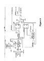
- a control circuit 100 comprising a switching clock 110 which is used to provide the time base or switching frequency for the PWM signal.
- This time base 110 can be a timer on the microcontroller, a PWM on the microcontroller, an external regularly timed signal or a irregular signal such as a zero current detect input or zero voltage detect input.
- the switching clock 110 may be adjustable, for example, by means of a digital control signal.
- the output controller 120 can be configured to set and reset a PWM output signal, thus controlling the pulse width.
- the switching clock 110 which as stated above may be adjustable determines the PWM switching frequency.
- the various embodiments can also be used to produce a single pulse (not a regular PWM signal but a monostable (one-shot) pulse of specified duration.
- the second major functional component is the duty cycle control 130 as shown in Fig. 1 .
- the duty cycle control 130 uses a clock source 140, which can be an oscillator clock, an internal regularly timed signal such as a timer or another PWM or an external signal provided through a microcontroller pin.
- This clock source 140 is connected through some logic gates 150 to the numerical controlled oscillator (NCO) peripheral 160 on the microcontroller.
- the NCO peripheral 160 is an overflow counter that implements Direct Digital Synthesis to produce a specified frequency by implementing an overflow counter which maintains the carry value in the accumulator.
- the increment register 170 is used to determine the switching frequency.
- the frequency produced by the NCO 160 is on average what has been set up in the increment register 170, this is achieved by occasionally emitting a pulse which is one clock faster than the normal pulse due to the carry in the accumulator causing an early overflow.
- the effect of this variation is that a higher average frequency is emitted.
- the output controller 120 combines the switching signal from switching clock 110 and the duty cycle controller 130 together starting the duty cycle controller clock only when the Switching Frequency Control has signaled a period start and disabling the duty cycle controller clock once the duty cycle pulse has been completed, leaving the system ready to receive the next Switching Frequency Control pulse and repeat the process.
- Fig. 2 shows an actual exemplary implementation using a microcontroller with at least two configurable logic cells and an NCO.
- a microcontroller is available from the assignee of the present application, for example the PIC16F1509 manufactured by Microchip Technology Inc., the documentation of which is hereby incorporated by reference.
- the first logic cell 220 is configured to form a D-flip flop U2 of the output controller 120.
- the second logic cell 230 is configured to form two AND gates U3, U4 and an OR gate U5. Input and output signals are then programmably routed to form the circuit as shown in Fig. 2 .
- dedicated logic can be implemented in a microcontroller that provides the same functionality.
- the operation of the circuit can be described as follows: 1.
- the flip-flop U2 will clock on the positive edge of the timing signal. This will cause the Q output to go high and the PWM pulse to start. 2.
- the AND gate U3 combines this output signal with a high-speed clock which is fed into the NCO clock pin via U5. At this point, the NCO output is low and U4 is not producing any output. 3.
- the NCO overflows, the NCO output goes high, which resets the flip-flop, forcing the Q output of the flip-flop to go low.
- U3 is now inactive due one of the two inputs of the gate being low. 4.
- U4 is used to get the NCO back to a stable state, as it needs an additional clock to return the NCO output to low.
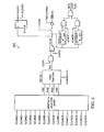
- Fig. 4 shows an exemplary numerical controlled oscillator that can be implemented as peripheral device within a microcontroller.
- the Numerically Controlled Oscillator (NCO) module 400 is a timer that uses the overflow from the addition of an increment value to divide the input frequency.
- the advantage of the addition method over simple counter driven timer is that the resolution of division does not vary with the divider value.
- the NCO 400 is most useful for applications that require frequency accuracy and fine resolution at a fixed duty cycle.
- Features of the NCO include: 16-bit increment function, Fixed Duty Cycle (FDC) mode, Pulse Frequency (PF) mode, Output pulse width control, Multiple clock input sources, Output polarity control, and Interrupt capability.
- FDC Fixed Duty Cycle
- PF Pulse Frequency
- the NCO module operates in a fixed duty cucle operation mode by repeatedly adding a fixed value stored in a register/buffer 410/420 to an accumulator 460 by means of an adder 430. Additions occur at the input clock rate provided by a multiplexer 440 and an enable gate 450.
- the accumulator 460 will overflow with a carry periodically, which is the raw NCO output signal.
- This output can be ANDed with the input clock by means of an AND gate 470 to generate an output signal, for example an interrupt signal NCOxIF.
- This signal can further be routed through other logic 480 as shown in Fig. 4 and fed to a multiplexer 490 to generate a final output signal NCOxOUT which is used as the output signal of the numerical controlled oscillator.
- Multiplexer 490 is used to select a pulse frequency modulation mode using the logic shown in the lower part of Fig. 4 which is not relevant for the present embodiments.
- D overflow NCO clock frequency * Increment Value / 2 n , wherein n is the accumulator width in bits.
- the NCO output can be further modified by the additional logic by stretching the pulse or toggling a flip-flop.
- the modified NCO output can then be distributed internally to other peripherals and optionally output to a pin.
- the accumulator overflow also generates an interrupt.
- the NCOx period changes in discrete steps to create an average frequency. This output depends on the ability of the receiving circuit to average the NCOx output to reduce uncertainty.
- the accumulator 460 can be, for example, a 20-bit register. Read and write access to the accumulator 460 may be available through three registers.
- the NCO Adder 430 can be a full adder, which operates independently from the system clock. The addition of the previous result and the increment value replaces the accumulator value on the rising edge of each input clock.
- the Increment value 410 can stored in two 8-bit registers 420 making up a 16-bit increment. Both of the registers can be readable and writeable.
- the Increment registers 410, 420 can be double-buffered to allow for value changes to be made without first disabling the NCO module 400.
- the buffer loads are immediate when the module is disabled. Writing to the increment register first is necessary because then the buffer 420 is loaded synchronously with the NCO operation after the write is executed on the Increment register 410.
- FDC Fixed Duty Cycle
- PF Pulse Frequency
- every time the accumulator 460 overflows the output becomes active for one or more clock periods. Once the clock period expires, the output returns to an inactive state. This provides a pulsed output. The output becomes active on the rising clock edge immediately following the overflow event.
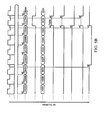
- a timing diagram is shown in Fig. 5 .
- the value of the active and inactive states depends on a polarity bit in the NCO control register.
- the PF mode is selected by setting a respective bit in the NCO control register.
- the active state of the output can vary in width by multiple clock periods.
- Various pulse widths are selected with respective bits in an NCO clock register. When the selected pulse width is greater than the accumulator overflow time frame, the output of the NCO operation is indeterminate.
- the last stage in the NCO module is the output polarity.
- the NxPOL bit in the NCO control register selects the output polarity. Changing the polarity while the interrupts are enabled will cause an interrupt for the resulting output transition.
- the NCO output can be used internally by source code or other peripherals.
- FIGS. 6 and 7 show examples of a programmable logic cell peripheral device according to various embodiments. However, as stated above, instead of programmable logic cells, dedicated logic can be implemented within a microcontroller to perform the same functions.
- the Configurable Logic Cell (CLCx) 600 provides programmable logic that operates outside the speed limitations of software execution.
- the logic cell receives up to 16 input signals and through the use of configurable input selection gates reduces the 16 inputs to four logic lines that drive one of, for example, eight selectable single-output logic functions.
- the input sources can be a combination of the following: I/O pins, Internal clocks, Peripherals, and Register bits.
- the output can be directed internally to peripherals and to an output pin.
- Fig. 6 shows for a simplified diagram showing signal flow through the CLCx, wherein x indicates a particular one of a plurality of configurable logic cells.
- possible configurations may include: Combinatorial Logic, such as AND, NAND, AND-OR, AND-OR-INVERT, OR-XOR, and OR-XNOR; and Latches such as S-R flip-flops, Clocked D-flip flops with Set and Reset, Transparent D- flip flops with Set and Reset, Clocked J-K flip flops with Reset.
- Programming the CLCx module 600 may be performed by configuring the 4 stages in the logic signal flow. The 4 stages are: Data selection, Data gating, Logic function selection, and Output polarity. Each stage can be setup at run time by writing to the corresponding CLCx Special Function Registers.
- Four 8-input multiplexers are used to select the inputs to pass on to the next stage.
- the 16 inputs to the multiplexers are arranged in groups of four. Each group is available to two of the four multiplexers, in each case, paired with a different group. This arrangement makes possible selection of up to two from a group without precluding a selection from another group.
- Data inputs are selected respective control registers. Data selection is through four multiplexers as indicated on the left side of Figure 6 . Data inputs in the figure are identified by a generic numbered input name.
- Table 1 below shows the pulse width, which this circuit will produce using a 16 MHz clock connected directly to the NCO clock input (FNCO), given various increment register values. Note that, for high increment values, a single increment of the register will change the pulse width by a mere 15 ps.
- TABLE 1 CALCULATED PWM PULSE WIDTH FOR DIFFERENT INCREMENT REGISTER VALUES Increment Value NCO FOUT (Hz) Average Pulse Width (ns) 65000 991,821 1,008.246 65001 991,837 1,008.231 20000 305,176 3,276.800 20001 305,191 3,276.636 100 1,526 655,360.000 101 1,541 648,871.287
- FIG. 8A shows the ripple of a conventional PWM modulator used in an SMPS.
- Fig. 8B shows the output signal of an SMPS with a PWM configured according to various embodiments of the present disclosure.
- the NCO 160 has thus a finely adjustable period. By averaging (dithering), the NCO period increments achievable are much smaller than the CPU clock and by using this period for the PWM pulse width the pulse width can be adjusted by increments effectively much smaller than the CPU clock.
- the overactive control loop thus will oscillate and can become unstable. Thus, a high speed control loop becomes a necessity.
- Table 2 shows a comparison of a conventional PWM with the PWM according to various embodiments.
- Table 2 Conventional PWM NCO Controlled PWM Clock Frequency 16 MHz 16 MHz Switching Frequency 1 MHz 1 MHz Ripple (@50% duty cycle) 12.5% 0.003% V IN 10V 10V V OUT 5V 5V V RIPPLE 0.625V 152uV Best PWM Pulse Adjustment 62.5ns 15.26ps Full Range PWM Resolution bits 16 bits 10% range PWM control Resolution 1 bit 13 bits
- the NCO is designed to give linear control over frequency.
- the control over pulse width is subsequently not linear.
- the pulse width will vary with the inverse of the frequency (1/x).
- the result is that the effective resolution of the PWM is not constant over the entire range from 0% to 100% duty cycle.
- the effective resolution can be calculated at this particular point, and can be plotted on a graph. This curve will look different depending on what the switching frequency is, because the pulse width is adjusted independently from the switching frequency.
- the PWM signal can be inverted when the duty cycle exceeds 50%. By doing this the performance under 50% duty cycle is effectively mirrored to the region above it, with the higher resolution. There is still the option to use the original curve where the limits of the increment are reached. This results in the graph as depicted in Figure 9C for the same conditions as the graph of Figure 9B .
- FIG. 9D shows the achievable resolution when using a 16 MHz clock at a switching frequency of 500 kHz with inversion at 50%.
- the PWM output produces an average pulse width. Although this is perfect for SMPS applications some other applications of PWMs may not be able to accommodate this. Also, the pulse adjustment resolution decreases as the switching frequency is decreased.
- the various embodiments can be implemented preferably in microcontrollers.
- the PWM can be triggered from an external signal such as a Zero current or Zero Voltage detector or comparator. This can be very important for efficiently switching FET's. A huge increase (4 bits to 16bits) in PWM resolution with no increase in cost can thus be accomplished.
- a PIC16F1509 manufactured by the assignee can be used to implement an embodiment according to this disclosure.
- This present embodiments allow for highly accurate SMPS control loops at extremely low power running at a fraction of the clock speeds of conventional systems, and still performing multiple orders of magnitude better.
- Higher switching speeds mean higher power densities which in turn means physically smaller and less expensive power supplies.
- One of the factors in SMPS design limiting switching frequency is that the PWM resolution decreases as the switching frequency increases.
Landscapes
- Physics & Mathematics (AREA)
- Spectroscopy & Molecular Physics (AREA)
- Engineering & Computer Science (AREA)
- Computer Networks & Wireless Communication (AREA)
- Signal Processing (AREA)
- Dc-Dc Converters (AREA)
- Dc Digital Transmission (AREA)
- Pulse Circuits (AREA)
- Stabilization Of Oscillater, Synchronisation, Frequency Synthesizers (AREA)
- Analogue/Digital Conversion (AREA)
Applications Claiming Priority (3)
| Application Number | Priority Date | Filing Date | Title |
|---|---|---|---|
| US201261602528P | 2012-02-23 | 2012-02-23 | |
| US13/773,177 US8873616B2 (en) | 2012-02-23 | 2013-02-21 | High resolution pulse width modulator |
| PCT/US2013/027216 WO2013126626A2 (en) | 2012-02-23 | 2013-02-22 | High resolution pulse width modulator |
Publications (2)
| Publication Number | Publication Date |
|---|---|
| EP2817885A2 EP2817885A2 (en) | 2014-12-31 |
| EP2817885B1 true EP2817885B1 (en) | 2016-01-13 |
Family
ID=49002843
Family Applications (1)
| Application Number | Title | Priority Date | Filing Date |
|---|---|---|---|
| EP13707260.9A Active EP2817885B1 (en) | 2012-02-23 | 2013-02-22 | High resolution pulse width modulator |
Country Status (8)
| Country | Link |
|---|---|
| US (1) | US8873616B2 (enExample) |
| EP (1) | EP2817885B1 (enExample) |
| JP (1) | JP6118827B2 (enExample) |
| KR (1) | KR101991886B1 (enExample) |
| CN (1) | CN104205634B (enExample) |
| ES (1) | ES2563854T3 (enExample) |
| TW (1) | TWI599178B (enExample) |
| WO (1) | WO2013126626A2 (enExample) |
Families Citing this family (5)
| Publication number | Priority date | Publication date | Assignee | Title |
|---|---|---|---|---|
| US9287884B2 (en) * | 2013-02-21 | 2016-03-15 | Microchip Technology Incorporated | Enhanced numerical controlled oscillator |
| US9363069B2 (en) | 2014-05-14 | 2016-06-07 | Novatek Microelectronics Corp. | Clock generating device and related synchronization method |
| WO2017075568A1 (en) * | 2015-10-29 | 2017-05-04 | Witricity Corporation | Controllers for wireless power systems |
| US11595027B2 (en) | 2021-03-01 | 2023-02-28 | Nxp Usa, Inc. | High frequency pulse width modulation shaping |
| TWI850072B (zh) * | 2023-08-21 | 2024-07-21 | 國立中山大學 | 數位脈衝寬度調變調變器 |
Family Cites Families (24)
| Publication number | Priority date | Publication date | Assignee | Title |
|---|---|---|---|---|
| JP2661222B2 (ja) * | 1988-12-19 | 1997-10-08 | 日本電気株式会社 | パルス出力装置 |
| US5144265A (en) * | 1990-07-19 | 1992-09-01 | Borg-Warner Automotive, Inc. | Pulse width modulation technique |
| JP3462786B2 (ja) * | 1999-03-30 | 2003-11-05 | 三洋電機株式会社 | デジタル復調装置 |
| JP3472527B2 (ja) * | 2000-05-16 | 2003-12-02 | 松下電器産業株式会社 | 論理回路モジュール及びこれを用いた半導体集積回路の設計方法並びに半導体集積回路 |
| US6606044B2 (en) * | 2002-01-02 | 2003-08-12 | Motorola, Inc. | Method and apparatus for generating a pulse width modulated signal |
| US6833691B2 (en) * | 2002-11-19 | 2004-12-21 | Power-One Limited | System and method for providing digital pulse width modulation |
| AU2003291888A1 (en) * | 2002-12-13 | 2004-07-09 | Yan-Fei Liu | Digital programmable pulse modulator with digital frequency control |
| WO2005041393A2 (en) * | 2003-10-24 | 2005-05-06 | Pf1, Inc. | Method and system for power factor correction |
| DE10355320B3 (de) * | 2003-11-27 | 2005-04-14 | Infineon Technologies Ag | Hochauflösender digitaler Pulsweitenmodulator und Verfahren zum Erzeugen eines hochaufgelösten pulsweitenmodulierten Signals |
| US7495565B2 (en) * | 2004-05-11 | 2009-02-24 | Sensomatic Electronics Corporation | Methods and apparatus for arbitrary antenna phasing in an electronic article surveillance system |
| US7466753B2 (en) * | 2004-12-01 | 2008-12-16 | Microchip Technology Incorporated | Microcontroller having a digital to frequency converter and/or a pulse frequency modulator |
| US7288977B2 (en) | 2005-01-21 | 2007-10-30 | Freescale Semiconductor, Inc. | High resolution pulse width modulator |
| US7327300B1 (en) * | 2005-08-25 | 2008-02-05 | Stmicroelectronics Pvt. Ltd. | System and method for generating a pulse width modulated signal having variable duty cycle resolution |
| US7378822B2 (en) * | 2005-11-17 | 2008-05-27 | Linear Technology Corporation | Switching regulator slope compensation generator circuit |
| US7459951B2 (en) | 2006-02-22 | 2008-12-02 | Exar Corporation | Self-calibrating digital pulse-width modulator (DPWM) |
| US7570037B2 (en) * | 2006-11-17 | 2009-08-04 | Virginia Tech Intellectual Properties, Inc. | Hybrid control methods for digital pulse width modulator (DPWM) |
| US7714626B2 (en) * | 2007-06-28 | 2010-05-11 | Microchip Technology Incorporated | System, method and apparatus having improved pulse width modulation frequency resolution |
| JP5165463B2 (ja) * | 2008-05-28 | 2013-03-21 | ルネサスエレクトロニクス株式会社 | Pwm制御装置及びパルス波形制御方法 |
| US8120401B2 (en) | 2008-11-21 | 2012-02-21 | L&L Engineering Llc | Methods and systems for digital pulse width modulator |
| US8698414B2 (en) * | 2009-04-13 | 2014-04-15 | Microchip Technology Incorporated | High resolution pulse width modulation (PWM) frequency control using a tunable oscillator |
| US8169245B2 (en) * | 2010-02-10 | 2012-05-01 | Freescale Semiconductor, Inc. | Duty transition control in pulse width modulation signaling |
| US9002488B2 (en) * | 2010-02-22 | 2015-04-07 | Cypress Semiconductor Corporation | Clock synthesis systems, circuits and methods |
| JP2012094934A (ja) * | 2010-10-22 | 2012-05-17 | Sharp Corp | パルス幅変調装置 |
| US8558497B2 (en) * | 2011-07-15 | 2013-10-15 | Cypress Semiconductor Corporation | Reduced electromagnetic interference for pulse-width modulation |
-
2013
- 2013-02-21 US US13/773,177 patent/US8873616B2/en active Active
- 2013-02-22 EP EP13707260.9A patent/EP2817885B1/en active Active
- 2013-02-22 WO PCT/US2013/027216 patent/WO2013126626A2/en not_active Ceased
- 2013-02-22 CN CN201380015649.4A patent/CN104205634B/zh active Active
- 2013-02-22 ES ES13707260.9T patent/ES2563854T3/es active Active
- 2013-02-22 JP JP2014558840A patent/JP6118827B2/ja active Active
- 2013-02-22 KR KR1020147026391A patent/KR101991886B1/ko not_active Expired - Fee Related
- 2013-02-23 TW TW102106474A patent/TWI599178B/zh active
Also Published As
| Publication number | Publication date |
|---|---|
| JP2015515769A (ja) | 2015-05-28 |
| TW201342808A (zh) | 2013-10-16 |
| CN104205634A (zh) | 2014-12-10 |
| KR20140135776A (ko) | 2014-11-26 |
| JP6118827B2 (ja) | 2017-04-19 |
| EP2817885A2 (en) | 2014-12-31 |
| TWI599178B (zh) | 2017-09-11 |
| US20130223508A1 (en) | 2013-08-29 |
| ES2563854T3 (es) | 2016-03-16 |
| KR101991886B1 (ko) | 2019-06-21 |
| US8873616B2 (en) | 2014-10-28 |
| WO2013126626A2 (en) | 2013-08-29 |
| CN104205634B (zh) | 2017-03-29 |
| WO2013126626A3 (en) | 2014-02-27 |
Similar Documents
| Publication | Publication Date | Title |
|---|---|---|
| US8120401B2 (en) | Methods and systems for digital pulse width modulator | |
| EP2817885B1 (en) | High resolution pulse width modulator | |
| US10642336B2 (en) | Clock adjustment for voltage droop | |
| US8558589B2 (en) | Fully digital method for generating sub clock division and clock waves | |
| US11545988B2 (en) | Method and apparatus for controlling clock cycle time | |
| US8125287B2 (en) | Extendable N-channel digital pulse-width/pulse-frequency modulator | |
| US10530375B1 (en) | High speed frequency divider | |
| CN202364200U (zh) | 一种基于数字延迟锁相环的数字脉宽调制器 | |
| US7881422B1 (en) | Circuits and methods for dividing frequency by an odd value | |
| EP1776764B1 (en) | Frequency divider | |
| US9287884B2 (en) | Enhanced numerical controlled oscillator | |
| CN112510975B (zh) | 一种用于提高加速器电源pwm精度的方法及系统 | |
| CN107547082B (zh) | 用于数字系统中时钟合成器的1-16和1.5-7.5分频器 | |
| US7327300B1 (en) | System and method for generating a pulse width modulated signal having variable duty cycle resolution | |
| US9391614B2 (en) | Clock state control for power saving in an integrated circuit | |
| US8269525B2 (en) | Logic cell having reduced spurious toggling | |
| CN105406844A (zh) | 一种支持输入输出模式的pwm架构 | |
| KR101018138B1 (ko) | 50퍼센트 듀티를 갖는 홀수 분주기 | |
| EP3270257A1 (en) | Clock adjustment for voltage droop | |
| US9312872B1 (en) | Signal converter | |
| US20140145774A1 (en) | Microcontroller with Digital Clock Source |
Legal Events
| Date | Code | Title | Description |
|---|---|---|---|
| PUAI | Public reference made under article 153(3) epc to a published international application that has entered the european phase |
Free format text: ORIGINAL CODE: 0009012 |
|
| 17P | Request for examination filed |
Effective date: 20140919 |
|
| AK | Designated contracting states |
Kind code of ref document: A2 Designated state(s): AL AT BE BG CH CY CZ DE DK EE ES FI FR GB GR HR HU IE IS IT LI LT LU LV MC MK MT NL NO PL PT RO RS SE SI SK SM TR |
|
| AX | Request for extension of the european patent |
Extension state: BA ME |
|
| DAX | Request for extension of the european patent (deleted) | ||
| GRAP | Despatch of communication of intention to grant a patent |
Free format text: ORIGINAL CODE: EPIDOSNIGR1 |
|
| INTG | Intention to grant announced |
Effective date: 20150727 |
|
| GRAS | Grant fee paid |
Free format text: ORIGINAL CODE: EPIDOSNIGR3 |
|
| GRAA | (expected) grant |
Free format text: ORIGINAL CODE: 0009210 |
|
| AK | Designated contracting states |
Kind code of ref document: B1 Designated state(s): AL AT BE BG CH CY CZ DE DK EE ES FI FR GB GR HR HU IE IS IT LI LT LU LV MC MK MT NL NO PL PT RO RS SE SI SK SM TR |
|
| REG | Reference to a national code |
Ref country code: GB Ref legal event code: FG4D |
|
| REG | Reference to a national code |
Ref country code: CH Ref legal event code: EP |
|
| REG | Reference to a national code |
Ref country code: IE Ref legal event code: FG4D |
|
| REG | Reference to a national code |
Ref country code: AT Ref legal event code: REF Ref document number: 771097 Country of ref document: AT Kind code of ref document: T Effective date: 20160215 Ref country code: CH Ref legal event code: NV Representative=s name: E. BLUM AND CO. AG PATENT- UND MARKENANWAELTE , CH |
|
| REG | Reference to a national code |
Ref country code: FR Ref legal event code: PLFP Year of fee payment: 4 |
|
| REG | Reference to a national code |
Ref country code: DE Ref legal event code: R096 Ref document number: 602013004638 Country of ref document: DE |
|
| REG | Reference to a national code |
Ref country code: ES Ref legal event code: FG2A Ref document number: 2563854 Country of ref document: ES Kind code of ref document: T3 Effective date: 20160316 |
|
| REG | Reference to a national code |
Ref country code: NL Ref legal event code: FP |
|
| REG | Reference to a national code |
Ref country code: LT Ref legal event code: MG4D |
|
| PG25 | Lapsed in a contracting state [announced via postgrant information from national office to epo] |
Ref country code: BE Free format text: LAPSE BECAUSE OF NON-PAYMENT OF DUE FEES Effective date: 20160229 |
|
| PG25 | Lapsed in a contracting state [announced via postgrant information from national office to epo] |
Ref country code: NO Free format text: LAPSE BECAUSE OF FAILURE TO SUBMIT A TRANSLATION OF THE DESCRIPTION OR TO PAY THE FEE WITHIN THE PRESCRIBED TIME-LIMIT Effective date: 20160413 Ref country code: GR Free format text: LAPSE BECAUSE OF FAILURE TO SUBMIT A TRANSLATION OF THE DESCRIPTION OR TO PAY THE FEE WITHIN THE PRESCRIBED TIME-LIMIT Effective date: 20160414 Ref country code: HR Free format text: LAPSE BECAUSE OF FAILURE TO SUBMIT A TRANSLATION OF THE DESCRIPTION OR TO PAY THE FEE WITHIN THE PRESCRIBED TIME-LIMIT Effective date: 20160113 Ref country code: FI Free format text: LAPSE BECAUSE OF FAILURE TO SUBMIT A TRANSLATION OF THE DESCRIPTION OR TO PAY THE FEE WITHIN THE PRESCRIBED TIME-LIMIT Effective date: 20160113 Ref country code: IT Free format text: LAPSE BECAUSE OF FAILURE TO SUBMIT A TRANSLATION OF THE DESCRIPTION OR TO PAY THE FEE WITHIN THE PRESCRIBED TIME-LIMIT Effective date: 20160113 |
|
| PG25 | Lapsed in a contracting state [announced via postgrant information from national office to epo] |
Ref country code: LV Free format text: LAPSE BECAUSE OF FAILURE TO SUBMIT A TRANSLATION OF THE DESCRIPTION OR TO PAY THE FEE WITHIN THE PRESCRIBED TIME-LIMIT Effective date: 20160113 Ref country code: LT Free format text: LAPSE BECAUSE OF FAILURE TO SUBMIT A TRANSLATION OF THE DESCRIPTION OR TO PAY THE FEE WITHIN THE PRESCRIBED TIME-LIMIT Effective date: 20160113 Ref country code: PL Free format text: LAPSE BECAUSE OF FAILURE TO SUBMIT A TRANSLATION OF THE DESCRIPTION OR TO PAY THE FEE WITHIN THE PRESCRIBED TIME-LIMIT Effective date: 20160113 Ref country code: PT Free format text: LAPSE BECAUSE OF FAILURE TO SUBMIT A TRANSLATION OF THE DESCRIPTION OR TO PAY THE FEE WITHIN THE PRESCRIBED TIME-LIMIT Effective date: 20160513 Ref country code: RS Free format text: LAPSE BECAUSE OF FAILURE TO SUBMIT A TRANSLATION OF THE DESCRIPTION OR TO PAY THE FEE WITHIN THE PRESCRIBED TIME-LIMIT Effective date: 20160113 Ref country code: SE Free format text: LAPSE BECAUSE OF FAILURE TO SUBMIT A TRANSLATION OF THE DESCRIPTION OR TO PAY THE FEE WITHIN THE PRESCRIBED TIME-LIMIT Effective date: 20160113 Ref country code: IS Free format text: LAPSE BECAUSE OF FAILURE TO SUBMIT A TRANSLATION OF THE DESCRIPTION OR TO PAY THE FEE WITHIN THE PRESCRIBED TIME-LIMIT Effective date: 20160513 |
|
| REG | Reference to a national code |
Ref country code: DE Ref legal event code: R097 Ref document number: 602013004638 Country of ref document: DE |
|
| PG25 | Lapsed in a contracting state [announced via postgrant information from national office to epo] |
Ref country code: MC Free format text: LAPSE BECAUSE OF FAILURE TO SUBMIT A TRANSLATION OF THE DESCRIPTION OR TO PAY THE FEE WITHIN THE PRESCRIBED TIME-LIMIT Effective date: 20160113 Ref country code: DK Free format text: LAPSE BECAUSE OF FAILURE TO SUBMIT A TRANSLATION OF THE DESCRIPTION OR TO PAY THE FEE WITHIN THE PRESCRIBED TIME-LIMIT Effective date: 20160113 Ref country code: EE Free format text: LAPSE BECAUSE OF FAILURE TO SUBMIT A TRANSLATION OF THE DESCRIPTION OR TO PAY THE FEE WITHIN THE PRESCRIBED TIME-LIMIT Effective date: 20160113 |
|
| PLBE | No opposition filed within time limit |
Free format text: ORIGINAL CODE: 0009261 |
|
| STAA | Information on the status of an ep patent application or granted ep patent |
Free format text: STATUS: NO OPPOSITION FILED WITHIN TIME LIMIT |
|
| PG25 | Lapsed in a contracting state [announced via postgrant information from national office to epo] |
Ref country code: SM Free format text: LAPSE BECAUSE OF FAILURE TO SUBMIT A TRANSLATION OF THE DESCRIPTION OR TO PAY THE FEE WITHIN THE PRESCRIBED TIME-LIMIT Effective date: 20160113 Ref country code: SK Free format text: LAPSE BECAUSE OF FAILURE TO SUBMIT A TRANSLATION OF THE DESCRIPTION OR TO PAY THE FEE WITHIN THE PRESCRIBED TIME-LIMIT Effective date: 20160113 Ref country code: RO Free format text: LAPSE BECAUSE OF FAILURE TO SUBMIT A TRANSLATION OF THE DESCRIPTION OR TO PAY THE FEE WITHIN THE PRESCRIBED TIME-LIMIT Effective date: 20160113 Ref country code: CZ Free format text: LAPSE BECAUSE OF FAILURE TO SUBMIT A TRANSLATION OF THE DESCRIPTION OR TO PAY THE FEE WITHIN THE PRESCRIBED TIME-LIMIT Effective date: 20160113 |
|
| 26N | No opposition filed |
Effective date: 20161014 |
|
| PG25 | Lapsed in a contracting state [announced via postgrant information from national office to epo] |
Ref country code: BE Free format text: LAPSE BECAUSE OF FAILURE TO SUBMIT A TRANSLATION OF THE DESCRIPTION OR TO PAY THE FEE WITHIN THE PRESCRIBED TIME-LIMIT Effective date: 20160113 |
|
| REG | Reference to a national code |
Ref country code: FR Ref legal event code: PLFP Year of fee payment: 5 |
|
| PG25 | Lapsed in a contracting state [announced via postgrant information from national office to epo] |
Ref country code: SI Free format text: LAPSE BECAUSE OF FAILURE TO SUBMIT A TRANSLATION OF THE DESCRIPTION OR TO PAY THE FEE WITHIN THE PRESCRIBED TIME-LIMIT Effective date: 20160113 Ref country code: BG Free format text: LAPSE BECAUSE OF FAILURE TO SUBMIT A TRANSLATION OF THE DESCRIPTION OR TO PAY THE FEE WITHIN THE PRESCRIBED TIME-LIMIT Effective date: 20160413 |
|
| PG25 | Lapsed in a contracting state [announced via postgrant information from national office to epo] |
Ref country code: MT Free format text: LAPSE BECAUSE OF FAILURE TO SUBMIT A TRANSLATION OF THE DESCRIPTION OR TO PAY THE FEE WITHIN THE PRESCRIBED TIME-LIMIT Effective date: 20160113 |
|
| REG | Reference to a national code |
Ref country code: FR Ref legal event code: PLFP Year of fee payment: 6 |
|
| PG25 | Lapsed in a contracting state [announced via postgrant information from national office to epo] |
Ref country code: HU Free format text: LAPSE BECAUSE OF FAILURE TO SUBMIT A TRANSLATION OF THE DESCRIPTION OR TO PAY THE FEE WITHIN THE PRESCRIBED TIME-LIMIT; INVALID AB INITIO Effective date: 20130222 |
|
| PG25 | Lapsed in a contracting state [announced via postgrant information from national office to epo] |
Ref country code: MT Free format text: LAPSE BECAUSE OF FAILURE TO SUBMIT A TRANSLATION OF THE DESCRIPTION OR TO PAY THE FEE WITHIN THE PRESCRIBED TIME-LIMIT Effective date: 20160229 Ref country code: LU Free format text: LAPSE BECAUSE OF NON-PAYMENT OF DUE FEES Effective date: 20160222 Ref country code: CY Free format text: LAPSE BECAUSE OF FAILURE TO SUBMIT A TRANSLATION OF THE DESCRIPTION OR TO PAY THE FEE WITHIN THE PRESCRIBED TIME-LIMIT Effective date: 20160113 Ref country code: MK Free format text: LAPSE BECAUSE OF FAILURE TO SUBMIT A TRANSLATION OF THE DESCRIPTION OR TO PAY THE FEE WITHIN THE PRESCRIBED TIME-LIMIT Effective date: 20160113 |
|
| PG25 | Lapsed in a contracting state [announced via postgrant information from national office to epo] |
Ref country code: AL Free format text: LAPSE BECAUSE OF FAILURE TO SUBMIT A TRANSLATION OF THE DESCRIPTION OR TO PAY THE FEE WITHIN THE PRESCRIBED TIME-LIMIT Effective date: 20160113 Ref country code: TR Free format text: LAPSE BECAUSE OF FAILURE TO SUBMIT A TRANSLATION OF THE DESCRIPTION OR TO PAY THE FEE WITHIN THE PRESCRIBED TIME-LIMIT Effective date: 20160113 |
|
| REG | Reference to a national code |
Ref country code: AT Ref legal event code: UEP Ref document number: 771097 Country of ref document: AT Kind code of ref document: T Effective date: 20160113 |
|
| P01 | Opt-out of the competence of the unified patent court (upc) registered |
Effective date: 20230528 |
|
| PGFP | Annual fee paid to national office [announced via postgrant information from national office to epo] |
Ref country code: NL Payment date: 20250121 Year of fee payment: 13 |
|
| PGFP | Annual fee paid to national office [announced via postgrant information from national office to epo] |
Ref country code: DE Payment date: 20250122 Year of fee payment: 13 |
|
| PGFP | Annual fee paid to national office [announced via postgrant information from national office to epo] |
Ref country code: ES Payment date: 20250303 Year of fee payment: 13 |
|
| PGFP | Annual fee paid to national office [announced via postgrant information from national office to epo] |
Ref country code: IE Payment date: 20250124 Year of fee payment: 13 |
|
| PGFP | Annual fee paid to national office [announced via postgrant information from national office to epo] |
Ref country code: AT Payment date: 20250124 Year of fee payment: 13 Ref country code: CH Payment date: 20250301 Year of fee payment: 13 |
|
| PGFP | Annual fee paid to national office [announced via postgrant information from national office to epo] |
Ref country code: FR Payment date: 20250122 Year of fee payment: 13 |
|
| PGFP | Annual fee paid to national office [announced via postgrant information from national office to epo] |
Ref country code: GB Payment date: 20250123 Year of fee payment: 13 |