EP2814307A1 - Bus bar - Google Patents
Bus bar Download PDFInfo
- Publication number
- EP2814307A1 EP2814307A1 EP13746691.8A EP13746691A EP2814307A1 EP 2814307 A1 EP2814307 A1 EP 2814307A1 EP 13746691 A EP13746691 A EP 13746691A EP 2814307 A1 EP2814307 A1 EP 2814307A1
- Authority
- EP
- European Patent Office
- Prior art keywords
- circuit board
- bus bar
- base part
- support columns
- pin
- Prior art date
- Legal status (The legal status is an assumption and is not a legal conclusion. Google has not performed a legal analysis and makes no representation as to the accuracy of the status listed.)
- Withdrawn
Links
Images




Classifications
-
- H—ELECTRICITY
- H02—GENERATION; CONVERSION OR DISTRIBUTION OF ELECTRIC POWER
- H02G—INSTALLATION OF ELECTRIC CABLES OR LINES, OR OF COMBINED OPTICAL AND ELECTRIC CABLES OR LINES
- H02G5/00—Installations of bus-bars
- H02G5/02—Open installations
- H02G5/025—Supporting structures
-
- H—ELECTRICITY
- H01—ELECTRIC ELEMENTS
- H01R—ELECTRICALLY-CONDUCTIVE CONNECTIONS; STRUCTURAL ASSOCIATIONS OF A PLURALITY OF MUTUALLY-INSULATED ELECTRICAL CONNECTING ELEMENTS; COUPLING DEVICES; CURRENT COLLECTORS
- H01R12/00—Structural associations of a plurality of mutually-insulated electrical connecting elements, specially adapted for printed circuits, e.g. printed circuit boards [PCB], flat or ribbon cables, or like generally planar structures, e.g. terminal strips, terminal blocks; Coupling devices specially adapted for printed circuits, flat or ribbon cables, or like generally planar structures; Terminals specially adapted for contact with, or insertion into, printed circuits, flat or ribbon cables, or like generally planar structures
- H01R12/50—Fixed connections
- H01R12/51—Fixed connections for rigid printed circuits or like structures
- H01R12/55—Fixed connections for rigid printed circuits or like structures characterised by the terminals
- H01R12/57—Fixed connections for rigid printed circuits or like structures characterised by the terminals surface mounting terminals
-
- H—ELECTRICITY
- H01—ELECTRIC ELEMENTS
- H01R—ELECTRICALLY-CONDUCTIVE CONNECTIONS; STRUCTURAL ASSOCIATIONS OF A PLURALITY OF MUTUALLY-INSULATED ELECTRICAL CONNECTING ELEMENTS; COUPLING DEVICES; CURRENT COLLECTORS
- H01R12/00—Structural associations of a plurality of mutually-insulated electrical connecting elements, specially adapted for printed circuits, e.g. printed circuit boards [PCB], flat or ribbon cables, or like generally planar structures, e.g. terminal strips, terminal blocks; Coupling devices specially adapted for printed circuits, flat or ribbon cables, or like generally planar structures; Terminals specially adapted for contact with, or insertion into, printed circuits, flat or ribbon cables, or like generally planar structures
- H01R12/70—Coupling devices
- H01R12/7005—Guiding, mounting, polarizing or locking means; Extractors
- H01R12/7011—Locking or fixing a connector to a PCB
- H01R12/7017—Snap means
-
- H—ELECTRICITY
- H01—ELECTRIC ELEMENTS
- H01R—ELECTRICALLY-CONDUCTIVE CONNECTIONS; STRUCTURAL ASSOCIATIONS OF A PLURALITY OF MUTUALLY-INSULATED ELECTRICAL CONNECTING ELEMENTS; COUPLING DEVICES; CURRENT COLLECTORS
- H01R43/00—Apparatus or processes specially adapted for manufacturing, assembling, maintaining, or repairing of line connectors or current collectors or for joining electric conductors
- H01R43/02—Apparatus or processes specially adapted for manufacturing, assembling, maintaining, or repairing of line connectors or current collectors or for joining electric conductors for soldered or welded connections
- H01R43/0256—Apparatus or processes specially adapted for manufacturing, assembling, maintaining, or repairing of line connectors or current collectors or for joining electric conductors for soldered or welded connections for soldering or welding connectors to a printed circuit board
-
- H—ELECTRICITY
- H01—ELECTRIC ELEMENTS
- H01R—ELECTRICALLY-CONDUCTIVE CONNECTIONS; STRUCTURAL ASSOCIATIONS OF A PLURALITY OF MUTUALLY-INSULATED ELECTRICAL CONNECTING ELEMENTS; COUPLING DEVICES; CURRENT COLLECTORS
- H01R43/00—Apparatus or processes specially adapted for manufacturing, assembling, maintaining, or repairing of line connectors or current collectors or for joining electric conductors
- H01R43/02—Apparatus or processes specially adapted for manufacturing, assembling, maintaining, or repairing of line connectors or current collectors or for joining electric conductors for soldered or welded connections
- H01R43/0263—Apparatus or processes specially adapted for manufacturing, assembling, maintaining, or repairing of line connectors or current collectors or for joining electric conductors for soldered or welded connections for positioning or holding parts during soldering or welding process
Definitions
- the present invention relates to a bus bar that is mounted on a board and performs electrical connection.
- JP2010-35304A discloses a surface-mounting bus bar in which one end of the bus bar is soldered to the surface of a circuit board.
- the plurality of bus bars are formed integrally by an insulating resin portion.
- JP2010-35304A when mounting the bus bar onto the board, a resin mold portion is prevented from moving on the board by inserting a pair of protrusions that protrude from a resin portion toward the circuit board side into through-holes formed in the circuit board.
- soldering operation e.g. reflow soldering
- heat at a high temperature suited to soldering is applied to the circuit board or bus bar.
- the thermal expansion coefficient of each also differs.
- the resin portion may deform relative to the circuit board due to the difference in the thermal expansion coefficients thereof.
- the bus bar that is fixed to the resin portion may rise up from the circuit board, and this may lead to defects in the soldering.
- the present invention was developed in view of the above problem and aims to provide a bus bar for mounting onto a board in which defects in the soldering can be prevented.
- a bus bar including a bus bar pin that is mounted onto a circuit board is privided.
- the bus bar includes a base part that is disposed along the circuit board and supports the bus bar pin and a pair of support columns that are formed at both ends of the base part and clamp the circuit board to fix the bus bar pin to the circuit board.
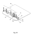
- FIGS. 1A and 1B are explanatory views of a circuit board 40 onto which a bus bar 10 is mounted of an embodiment of the present invention.
- FIG. 1A is a schematic view of the side of the circuit board 40 onto which the bus bar 10 is mounted
- FIG. 1B is a schematic view of the side opposite to the side of the circuit board 40 onto which the bus bar 10 is mounted.
- Circuit components such as electronic components and the bus bar 10 are mounted onto the circuit board 40.
- the electronic components are omitted from FIGS. 1A and 1B .
- the bus bar 10 is fixed to the circuit board 40 and mounted by soldering.
- the circuit board 40 of the present embodiment is constituted by using a metal such as aluminum or copper as a base material and subjecting the surface thereof to an insulating treatment, circuit patterning, and the like.
- a metal such as aluminum or copper
- the circuit board 40 exhibits increased thermal conductivity, and thus is suited to mounting electronic components that produce large amounts of heat such as power semiconductors and the like.
- the bus bar 10 includes a plurality of bus par pins 11 that extend upwards in the vertical direction relative to the circuit board 40.
- the bus bar pins 11 electrically connect to the other circuit board or functional component to transmit and receive signals and electric power between the circuit board 40 and the other circuit board or functional component.
- the bus bar 10 is constituted by fixing the plurality of bus bar pins 11 to a base part 20.
- the base part 20 is constituted by, for example, a non-electrically conductive resin or the like, and is arranged along the surface of the circuit board 40.
- the plurality of bus bar pins 11 are integrally molded by the base part 20 made of resin, thereby constituting the bus bar 10.
- a pair of support columns 25 for fixing the bus bar 10 to the circuit board 40 is formed at both ends of the base part 20.
- the bus par pins 11 are constituted by an electrically conductive metal such as copper or nickel.
- the bus bar pins 11 are subjected to a surface treatment suited for performing soldering.
- the bus par pins 11 include bus par pins 11 a having a prismatic column-shaped cross section and bus bar pins 11b having a panel-shaped cross section.
- the bus bar pins 11b are used for transmitting and receiving larger amounts of electrical power than the bus bar pins 11a.
- Each bus bar pin 11 is formed integrally by a vertical part 14 that extends upwards from the base part 20 in the vertical direction relative to the circuit board 40, a pin foot part 12 that extends downwards from the base part 20 in the vertical direction relative to the circuit board 40 side, and a connecting part 13 that connects the vertical part 14 and the pin foot part 12.
- a bottom part 12a that forms a surface that is approximately parallel to the circuit board 40 is formed at the bottom end of the pin foot part 12. The bottom part 12a is bonded by soldering to a land 42 disposed on the circuit board 40.
- Each electrically conductive land 42 is disposed at a position on the circuit board 40 corresponding to the bottom part 12a of each pin foot part 12. Further, a pair of recesses 45 is formed on both side surfaces of the circuit board 40 at positions corresponding to the pair of support columns 25 of the bus bar 10. The recesses 45 are formed by hollowing out semicircular shapes in mutually approaching directions from the side surface sides of the circuit board 40.
- the bus bar 10 is fixed to the circuit board 40 by fitting the pair of support columns 25 of the bus bar 10 into the recesses 45 of the circuit board 40.
- Each of the pair of support columns 25 includes a main body part 26 that is joined at both ends of the base part 20 and abuts the surface of the circuit board 40, and a fitting part 27 that is formed to extend downwards from the main body part 26 and fits into the recess 45.
- the shape of the inner surface side of each fitting part 27 corresponds to an outer peripheral side of the recess 45 formed in the circuit board 40.
- Each fitting part 27 is formed with a cross section area that is smaller than that of the main body part 26.
- a stepped part 26a is formed between the main body part 26 and the fitting part 27. The stepped part 26a abuts the surface of the circuit board 40.
- a positioning pin 30 that is formed to extend toward the circuit board 40 side is included at an intermediate portion in the lengthwise direction of the base part 20.
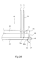
- FIGS. 2A and 2B are explanatory views of the main parts of the bus bar 10 and the circuit board 40 with a focus on the support columns 25 of the embodiment of the present invention.
- FIG. 2A is a schematic view focused on one support column 25.
- FIG. 2B is a side surface perspective view from the side (when viewed from the arrow B direction) of the support column 25.
- the support columns 25 are formed to extend toward the circuit board 40 side at both ends of the base part 20.
- Each support column 25 includes the main body part 26 and the fitting part 27.
- Each fitting part 27 has a shape that corresponds to the recess 45 formed in the circuit board 40. Given this constitution, the pair of fitting parts 27 that respectively extend from the pair of support columns 25 fit into the circuit board 40 from both side surface sides of the circuit board 40. Thereby, the support columns 25 clamp the circuit board 40 from both side surface sides to fix the bus bar 10 to the circuit board 40.
- Pawl parts 28 formed in mutually approaching directions are respectively formed on the distal ends of the pair of fitting parts 27.
- the pawl parts 28 lock onto the underside surface of the circuit board 40.
- the stepped part 26a of each support column 25 abuts the surface of the circuit board 40 and the pawl part 28 formed on the fitting part 27 engages with the underside surface side of the circuit board 40. Therefore, the stepped part 26a and the pawl part 28 grip the circuit board 40 in the board thickness direction.
- the support columns 25 fix the circuit board 40 in the board thickness direction and the bus bar 10 is fixed in the board thickness direction of the circuit board 40.
- FIGS. 3A and 3B are explanatory views of the bus bar 10 and the circuit board 40 of the embodiment of the present invention.
- FIG. 3A illustrates a top surface view of the circuit board 40
- FIG. 3B illustrates a cross section view along line 33A-33A shown in FIG. 3A .
- the positioning pin 30 is formed at a position corresponding to a positioning hole 46 formed in the circuit board 40. When fixing the base part 20 to the circuit board 40, the positioning pin 30 is inserted into the positioning hole 46.
- the positioning pin 30 has a sporked structure, and a positioning pin pawl part 31 is formed on each distal end of the sporked structure of the positioning pin 30.
- the positioning pin pawl parts 31 engage with the underside surface of the circuit board 40. Thereby, the positioning pin 30 is fixed to the circuit board 40.
- soldering paste is applied in advance onto the lands 42 of the circuit board 40, and then a process for fixing the bus bar 10 onto the circuit board 40 on which the soldering paste has been applied is performed.
- the support columns 25 extending at both end sides of the base part 20 of the bus bar 10 are attached to the recesses 45 formed on both side surfaces of the circuit board 40.
- the fitting parts 27 are fitted from both side surface sides of the circuit board 40 into the recesses 45 which are cut out in semicircular shapes from the side surfaces of the circuit board 40. Thereby, the fitting parts 27 clamp the circuit board 40 from both side surface sides. Further, the pawl parts 28 engage with the circuit board 40 from the underside surface side of the circuit board 40. Thereby, the circuit board 40 is gripped in the board thickness direction by the stepped parts 26a and the pawl parts 28.
- the positioning pin 30 that extends at an intermediate portion of the base part 20 is fitted into the positioning hole 46 of the circuit board 40.
- the positioning pin pawl parts 31 at the distal end of the positioning pin 30 engage with the positioning hole 46 from the underside surface side of the circuit board 40.
- the bus bar 10 is fixed to the circuit board 40 as described above.
- Other electronic components and the like to be mounted onto the circuit board 40 are attached with an adhesive or the like to the circuit board 40.
- the soldering process is carried out.
- the soldering process is carried out by reflow.
- Reflow is a process for soldering electronic components in which an electronic component such as the bus bar 10 is fixed to the circuit board 40 to which a soldering paste has been applied onto the lands 42 in advance and then the soldering is melted by heating in a reflow furnace.
- the circuit board 40 to which the bus bar 10 has been fixed is inserted into a reflow furnace.
- the reflow furnace heats the circuit board 40 at a temperature and for a duration suitable for melting the soldering paste.
- the circuit board 40 After the completion of heating in the reflow furnace, the circuit board 40 is removed from the reflow furnace and the temperature thereof is lowered to room temperature. Thereby, the soldering process by reflow is complete, and the bus bar 10 is mounted to the circuit board 40.
- the circuit board 40 of the present embodiment is constituted by a metal base material such as aluminum.
- the bus bar 10 in order to secure the insulating properties between the bus bar pins 11 and to increase the manufacturability and mountability, the base part 20 is constituted by a resin. Therefore, the thermal expansion coefficient due to heat of the bus bar 10 is different from that of the circuit board 40.
- the bus bar is fixed by screws at both ends to the circuit board as in the conventional technology, the bus bar is subjected to stress from the difference in the thermal expansion coefficients.
- the thermal expansion coefficient of the base part of the bus bar is larger than the thermal expansion coefficient of the circuit board, the bus bar fixed at both ends may deform, causing an intermediate portion thereof to rise up from the circuit board. If the bus bar rises up from the circuit board, the bottom parts of the pin foot parts of the bus bar pins may rise off of the lands causing defects in the soldering.
- the bus bar 10 of the present embodiment is constituted such that the support columns 25 of the bus bar 10 clamp the circuit board 40 from both side surface sides.
- the thermal expansion coefficient of the base part 20 is larger than the thermal expansion coefficient of the circuit board 40, there is room for the support columns 25 at both ends of the base part 20 to escape towards the outside of the recesses 45 of the circuit board 40.
- Deformation of the base part 20 can be suppressed by allowing the support columns 25 to escape to the outside, and thus the bus bar 10 can be prevented from rising up from the circuit board 40. Therefore, the bottom parts 12a of the pin foot parts 12 of the bus bar pins 11 are also prevented from rising off the lands 42, and thereby soldering defects can be prevented.
- the fitting parts 27 of the bus bar 10 fit into the recesses 45 of the circuit board 40 to clamp the circuit board 40 from both side surfaces. Further, the circuit board 40 is gripped in the board thickness direction by the stepped parts 26a and the pawl parts 28. Given this constitution, the bus bar 10 can be fixed such that it cannot easily come off from the circuit board 40.
- the bus bar 10 includes the positioning pin 30 at an intermediate portion thereof, and the positioning pin pawl parts 31 of the positioning pin 30 are inserted into the positioning hole 46 to lock onto the underside surface of the circuit board 40.
- the intermediate portion of the bus bar 10 can be fixed in a direction in which it is pressed to the circuit board 40.
- any individual difference in the base part 20 is absorbed and the bottom parts 12a of the pin foot parts 12 are pressed to the lands 42 to adhere the bottom parts 12a to the lands 42, and thereby soldering defects can be prevented.
- the positioning pin 30 is preferably provided at only one location within the intermediate portion in the lengthwise direction of the base part 20, but positioning pins 30 can be provided at two or more locations therein.
- the bus bar pins 11 are fixed to the circuit board 40 by clamping the circuit board 40 with the pair of support columns 25 formed at both ends of the base part 20.
- the bus bar pins 11 can be prevented from rising up from the circuit board 40, and thereby defects in the soldering of the bus bar 10 can also be prevented.
- the fitting parts 27 are fitted into the recesses 45 formed by cutting out both side surface sides of the circuit board 40.
- the shape of the recesses 45 is not limited thereto.
- fixing holes having an elliptical or elongated hole shape can be formed at two locations in the circuit board 40, and these two fixing holes can be clamped by the fitting parts 27.
- the recesses 45 are also not limited to these shapes, and any shape is acceptable as long as the recesses 45 realize a structure that allows for the two support columns 25 on the base part 20 to escape toward the outside.
- circuit board 40 of the above-described embodiment of the present invention is constituted by a metallic base material.
- it can also be constituted by another material such as glass epoxy.
Landscapes
- Coupling Device And Connection With Printed Circuit (AREA)
- Multi-Conductor Connections (AREA)
Abstract
Description
- The present invention relates to a bus bar that is mounted on a board and performs electrical connection.
- In a circuit board on which an electronic circuit is mounted, for example, a metal bus bar that transmits and receives electric power and signals between a circuit board and another circuit board has been conventionally mounted on a circuit board. As a method for mounting a bus bar on a circuit board,
JP2010-35304A - In the conventional technology disclosed in
JP2010-35304A - In a soldering operation, e.g. reflow soldering, for mounting a bus bar onto a circuit board, heat at a high temperature suited to soldering is applied to the circuit board or bus bar. At this time, since the material properties of the resin portion and the circuit board differ, the thermal expansion coefficient of each also differs.
- Therefore, if the resin portion is fixed to the circuit board such that it cannot move as explained above, the resin portion may deform relative to the circuit board due to the difference in the thermal expansion coefficients thereof. In particular, if the resin portion warps and deforms in a direction away from the circuit board, the bus bar that is fixed to the resin portion may rise up from the circuit board, and this may lead to defects in the soldering.
- The present invention was developed in view of the above problem and aims to provide a bus bar for mounting onto a board in which defects in the soldering can be prevented.
- According to an embodiment of the present invention, a bus bar including a bus bar pin that is mounted onto a circuit board is privided. The bus bar includes a base part that is disposed along the circuit board and supports the bus bar pin and a pair of support columns that are formed at both ends of the base part and clamp the circuit board to fix the bus bar pin to the circuit board.
- Embodiments of the present invention and advantages of the present invention will be explained in detail below together with reference to the attached drawings.
-
-
FIG. 1A is a schematic view of a circuit board onto which a bus bar is mounted of an embodiment of the present invention; -
FIG. 1B is a schematic view of the circuit board onto which a bus bar is mounted of the embodiment of the present invention; -
FIG. 2A is an explanatory view of the main parts of the bus bar and the circuit board of the embodiment of the present invention; -
FIG. 2B is an explanatory view of the main parts of the bus bar and the circuit board of the embodiment of the present invention; -
FIG. 3A is a top surface view of the circuit board onto which a bus bar is mounted of the embodiment of the present invention; and -
FIG. 3B is a cross-section view of the circuit board onto which a bus bar is mounted of the embodiment of the present invention. - Embodiments of the present invention will now be explained with reference to the drawings.
-
FIGS. 1A and1B are explanatory views of acircuit board 40 onto which abus bar 10 is mounted of an embodiment of the present invention.FIG. 1A is a schematic view of the side of thecircuit board 40 onto which thebus bar 10 is mounted, andFIG. 1B is a schematic view of the side opposite to the side of thecircuit board 40 onto which thebus bar 10 is mounted. - Circuit components such as electronic components and the
bus bar 10 are mounted onto thecircuit board 40. The electronic components are omitted fromFIGS. 1A and1B . Thebus bar 10 is fixed to thecircuit board 40 and mounted by soldering. - The
circuit board 40 of the present embodiment is constituted by using a metal such as aluminum or copper as a base material and subjecting the surface thereof to an insulating treatment, circuit patterning, and the like. By constituting the base material with a metal as described above, thecircuit board 40 exhibits increased thermal conductivity, and thus is suited to mounting electronic components that produce large amounts of heat such as power semiconductors and the like. - The
bus bar 10 includes a plurality ofbus par pins 11 that extend upwards in the vertical direction relative to thecircuit board 40. When another circuit board or functional component is arranged above thecircuit board 40, thebus bar pins 11 electrically connect to the other circuit board or functional component to transmit and receive signals and electric power between thecircuit board 40 and the other circuit board or functional component. - The
bus bar 10 is constituted by fixing the plurality ofbus bar pins 11 to abase part 20. Thebase part 20 is constituted by, for example, a non-electrically conductive resin or the like, and is arranged along the surface of thecircuit board 40. The plurality ofbus bar pins 11 are integrally molded by thebase part 20 made of resin, thereby constituting thebus bar 10. A pair ofsupport columns 25 for fixing thebus bar 10 to thecircuit board 40 is formed at both ends of thebase part 20. - The
bus par pins 11 are constituted by an electrically conductive metal such as copper or nickel. Thebus bar pins 11 are subjected to a surface treatment suited for performing soldering. In the present embodiment, thebus par pins 11 includebus par pins 11 a having a prismatic column-shaped cross section andbus bar pins 11b having a panel-shaped cross section. Thebus bar pins 11b are used for transmitting and receiving larger amounts of electrical power than thebus bar pins 11a. - Each
bus bar pin 11 is formed integrally by avertical part 14 that extends upwards from thebase part 20 in the vertical direction relative to thecircuit board 40, apin foot part 12 that extends downwards from thebase part 20 in the vertical direction relative to thecircuit board 40 side, and a connectingpart 13 that connects thevertical part 14 and thepin foot part 12. Abottom part 12a that forms a surface that is approximately parallel to thecircuit board 40 is formed at the bottom end of thepin foot part 12. Thebottom part 12a is bonded by soldering to aland 42 disposed on thecircuit board 40. - Each electrically
conductive land 42 is disposed at a position on thecircuit board 40 corresponding to thebottom part 12a of eachpin foot part 12. Further, a pair ofrecesses 45 is formed on both side surfaces of thecircuit board 40 at positions corresponding to the pair ofsupport columns 25 of thebus bar 10. Therecesses 45 are formed by hollowing out semicircular shapes in mutually approaching directions from the side surface sides of thecircuit board 40. Thebus bar 10 is fixed to thecircuit board 40 by fitting the pair ofsupport columns 25 of thebus bar 10 into therecesses 45 of thecircuit board 40. - Each of the pair of
support columns 25 includes amain body part 26 that is joined at both ends of thebase part 20 and abuts the surface of thecircuit board 40, and afitting part 27 that is formed to extend downwards from themain body part 26 and fits into therecess 45. The shape of the inner surface side of each fitting part 27 (surfaces on the sides of the pair offitting parts 27 that face each other) corresponds to an outer peripheral side of therecess 45 formed in thecircuit board 40. - Each
fitting part 27 is formed with a cross section area that is smaller than that of themain body part 26. Astepped part 26a is formed between themain body part 26 and thefitting part 27. Thestepped part 26a abuts the surface of thecircuit board 40. - A
positioning pin 30 that is formed to extend toward thecircuit board 40 side is included at an intermediate portion in the lengthwise direction of thebase part 20. -
FIGS. 2A and2B are explanatory views of the main parts of thebus bar 10 and thecircuit board 40 with a focus on thesupport columns 25 of the embodiment of the present invention.FIG. 2A is a schematic view focused on onesupport column 25.FIG. 2B is a side surface perspective view from the side (when viewed from the arrow B direction) of thesupport column 25. - The
support columns 25 are formed to extend toward thecircuit board 40 side at both ends of thebase part 20. Eachsupport column 25 includes themain body part 26 and thefitting part 27. Eachfitting part 27 has a shape that corresponds to therecess 45 formed in thecircuit board 40. Given this constitution, the pair offitting parts 27 that respectively extend from the pair ofsupport columns 25 fit into thecircuit board 40 from both side surface sides of thecircuit board 40. Thereby, thesupport columns 25 clamp thecircuit board 40 from both side surface sides to fix thebus bar 10 to thecircuit board 40. -
Pawl parts 28 formed in mutually approaching directions are respectively formed on the distal ends of the pair offitting parts 27. Thepawl parts 28 lock onto the underside surface of thecircuit board 40. Given this constitution, the steppedpart 26a of eachsupport column 25 abuts the surface of thecircuit board 40 and thepawl part 28 formed on thefitting part 27 engages with the underside surface side of thecircuit board 40. Therefore, the steppedpart 26a and thepawl part 28 grip thecircuit board 40 in the board thickness direction. Thereby, thesupport columns 25 fix thecircuit board 40 in the board thickness direction and thebus bar 10 is fixed in the board thickness direction of thecircuit board 40. -
FIGS. 3A and3B are explanatory views of thebus bar 10 and thecircuit board 40 of the embodiment of the present invention.FIG. 3A illustrates a top surface view of thecircuit board 40, andFIG. 3B illustrates a cross section view alongline 33A-33A shown inFIG. 3A . - The
positioning pin 30 is formed at a position corresponding to apositioning hole 46 formed in thecircuit board 40. When fixing thebase part 20 to thecircuit board 40, thepositioning pin 30 is inserted into thepositioning hole 46. - The
positioning pin 30 has a sporked structure, and a positioningpin pawl part 31 is formed on each distal end of the sporked structure of thepositioning pin 30. The positioningpin pawl parts 31 engage with the underside surface of thecircuit board 40. Thereby, thepositioning pin 30 is fixed to thecircuit board 40. - Next, the process for mounting the
bus bar 10 that is constituted as described above onto thecircuit board 40 will be explained. - When mounting the
bus board 10 onto thecircuit board 40, first, soldering paste is applied in advance onto thelands 42 of thecircuit board 40, and then a process for fixing thebus bar 10 onto thecircuit board 40 on which the soldering paste has been applied is performed. In this process, thesupport columns 25 extending at both end sides of thebase part 20 of thebus bar 10 are attached to therecesses 45 formed on both side surfaces of thecircuit board 40. - In more detail, the
fitting parts 27 are fitted from both side surface sides of thecircuit board 40 into therecesses 45 which are cut out in semicircular shapes from the side surfaces of thecircuit board 40. Thereby, thefitting parts 27 clamp thecircuit board 40 from both side surface sides. Further, thepawl parts 28 engage with thecircuit board 40 from the underside surface side of thecircuit board 40. Thereby, thecircuit board 40 is gripped in the board thickness direction by the steppedparts 26a and thepawl parts 28. - Next, the
positioning pin 30 that extends at an intermediate portion of thebase part 20 is fitted into thepositioning hole 46 of thecircuit board 40. At this time, the positioningpin pawl parts 31 at the distal end of thepositioning pin 30 engage with thepositioning hole 46 from the underside surface side of thecircuit board 40. - The
bus bar 10 is fixed to thecircuit board 40 as described above. Other electronic components and the like to be mounted onto thecircuit board 40 are attached with an adhesive or the like to thecircuit board 40. - After the
bus bar 10 has been fixed to thecircuit board 40, the soldering process is carried out. In the present embodiment, the soldering process is carried out by reflow. Reflow is a process for soldering electronic components in which an electronic component such as thebus bar 10 is fixed to thecircuit board 40 to which a soldering paste has been applied onto thelands 42 in advance and then the soldering is melted by heating in a reflow furnace. - In reflow, the
circuit board 40 to which thebus bar 10 has been fixed is inserted into a reflow furnace. The reflow furnace heats thecircuit board 40 at a temperature and for a duration suitable for melting the soldering paste. - After the completion of heating in the reflow furnace, the
circuit board 40 is removed from the reflow furnace and the temperature thereof is lowered to room temperature. Thereby, the soldering process by reflow is complete, and thebus bar 10 is mounted to thecircuit board 40. - Herein, the
circuit board 40 of the present embodiment is constituted by a metal base material such as aluminum. Meanwhile, with regard to thebus bar 10, in order to secure the insulating properties between the bus bar pins 11 and to increase the manufacturability and mountability, thebase part 20 is constituted by a resin. Therefore, the thermal expansion coefficient due to heat of thebus bar 10 is different from that of thecircuit board 40. - Thus, for example, if the bus bar is fixed by screws at both ends to the circuit board as in the conventional technology, the bus bar is subjected to stress from the difference in the thermal expansion coefficients. In particular, if the thermal expansion coefficient of the base part of the bus bar is larger than the thermal expansion coefficient of the circuit board, the bus bar fixed at both ends may deform, causing an intermediate portion thereof to rise up from the circuit board. If the bus bar rises up from the circuit board, the bottom parts of the pin foot parts of the bus bar pins may rise off of the lands causing defects in the soldering.
- In contrast, the
bus bar 10 of the present embodiment is constituted such that thesupport columns 25 of thebus bar 10 clamp thecircuit board 40 from both side surface sides. Given this constitution, even if the thermal expansion coefficient of thebase part 20 is larger than the thermal expansion coefficient of thecircuit board 40, there is room for thesupport columns 25 at both ends of thebase part 20 to escape towards the outside of therecesses 45 of thecircuit board 40. Deformation of thebase part 20 can be suppressed by allowing thesupport columns 25 to escape to the outside, and thus thebus bar 10 can be prevented from rising up from thecircuit board 40. Therefore, thebottom parts 12a of thepin foot parts 12 of the bus bar pins 11 are also prevented from rising off thelands 42, and thereby soldering defects can be prevented. - The
fitting parts 27 of thebus bar 10 fit into therecesses 45 of thecircuit board 40 to clamp thecircuit board 40 from both side surfaces. Further, thecircuit board 40 is gripped in the board thickness direction by the steppedparts 26a and thepawl parts 28. Given this constitution, thebus bar 10 can be fixed such that it cannot easily come off from thecircuit board 40. - The
bus bar 10 includes thepositioning pin 30 at an intermediate portion thereof, and the positioningpin pawl parts 31 of thepositioning pin 30 are inserted into thepositioning hole 46 to lock onto the underside surface of thecircuit board 40. Given this constitution, the intermediate portion of thebus bar 10 can be fixed in a direction in which it is pressed to thecircuit board 40. Thus, any individual difference in thebase part 20 is absorbed and thebottom parts 12a of thepin foot parts 12 are pressed to thelands 42 to adhere thebottom parts 12a to thelands 42, and thereby soldering defects can be prevented. Thepositioning pin 30 is preferably provided at only one location within the intermediate portion in the lengthwise direction of thebase part 20, but positioning pins 30 can be provided at two or more locations therein. - Therefore, in this embodiment of the present invention, the bus bar pins 11 are fixed to the
circuit board 40 by clamping thecircuit board 40 with the pair ofsupport columns 25 formed at both ends of thebase part 20. Given this constitution, for example, even if thebase part 20 deforms relative to thecircuit board 40 due to a difference in the thermal expansion coefficients when heating thebus bar 10 and thecircuit board 40 by reflow or the like, deformation of thebase part 20 due to thermal expansion can be suppressed because the pair ofsupport columns 25 which are not fixed to thecircuit board 40 can escape in a direction away from thecircuit board 40. Thus, the bus bar pins 11 can be prevented from rising up from thecircuit board 40, and thereby defects in the soldering of thebus bar 10 can also be prevented. - In the embodiment of the present invention explained above, the
fitting parts 27 are fitted into therecesses 45 formed by cutting out both side surface sides of thecircuit board 40. However, the shape of therecesses 45 is not limited thereto. For example, fixing holes having an elliptical or elongated hole shape can be formed at two locations in thecircuit board 40, and these two fixing holes can be clamped by thefitting parts 27. Further, therecesses 45 are also not limited to these shapes, and any shape is acceptable as long as therecesses 45 realize a structure that allows for the twosupport columns 25 on thebase part 20 to escape toward the outside. - In addition, the
circuit board 40 of the above-described embodiment of the present invention is constituted by a metallic base material. However, it can also be constituted by another material such as glass epoxy. - Embodiments of the present invention have been explained above, but these embodiments merely describe some of the applicable examples of the present invention, and the technical scope of the present invention should not be construed as limited to the specific constitutions of the embodiments described above.
- This application is based on and claims priority to Japanese Patent Application No.
2012-22864 - The exclusive properties or characteristics of the embodiments of the present invention are claimed as follows.
Claims (6)
- A bus bar including a bus bar pin that is configured to mount onto a circuit board, the bus bar comprising:a base part that is configured to dispose along the circuit board and is configured to support the bus bar pin, anda pair of support columns that are configured to form at both ends of the base part and clamp the circuit board to fix the bus bar pin to the circuit board.
- The bus bar according to claim 1, wherein recesses are configured to form on both side surfaces of the circuit board, and the support columns are configured to fit into the recesses.
- The bus bar according to claim 1, wherein a pawl part that configured to lock onto an underside surface of the circuit board is formed at an end of each support column.
- The bus bar according to claim 2, wherein each support column includes a main body part that is joined to the base part and abuts the surface of the circuit board and a fitting part that extends from the main body part and fits into the recess, and
the support columns configured to grip the circuit board in a board thickness direction by stepped parts formed between the main body part and the fitting part and the pawl parts. - The bus bar according to claim 1, wherein a positioning pin configured to be formed on the base part between the support columns, and the positioning pin is inserted into a positioning hole formed in the circuit board.
- The bus bar according to claim 5, wherein a positioning pin pawl part that configured to lock onto an underside surface of the circuit board is formed at a distal end of the positioning pin.
Applications Claiming Priority (2)
| Application Number | Priority Date | Filing Date | Title |
|---|---|---|---|
| JP2012022864A JP6088143B2 (en) | 2012-02-06 | 2012-02-06 | Bus bar |
| PCT/JP2013/050549 WO2013118540A1 (en) | 2012-02-06 | 2013-01-15 | Bus bar |
Publications (2)
| Publication Number | Publication Date |
|---|---|
| EP2814307A1 true EP2814307A1 (en) | 2014-12-17 |
| EP2814307A4 EP2814307A4 (en) | 2015-09-30 |
Family
ID=48947309
Family Applications (1)
| Application Number | Title | Priority Date | Filing Date |
|---|---|---|---|
| EP13746691.8A Withdrawn EP2814307A4 (en) | 2012-02-06 | 2013-01-15 | OMNIBUS BAR |
Country Status (5)
| Country | Link |
|---|---|
| US (1) | US9425602B2 (en) |
| EP (1) | EP2814307A4 (en) |
| JP (1) | JP6088143B2 (en) |
| CN (1) | CN104094680B (en) |
| WO (1) | WO2013118540A1 (en) |
Families Citing this family (4)
| Publication number | Priority date | Publication date | Assignee | Title |
|---|---|---|---|---|
| JP6960573B2 (en) * | 2016-12-22 | 2021-11-05 | パナソニックIpマネジメント株式会社 | Busbar unit and motor drive |
| CN112009202B (en) * | 2019-05-31 | 2024-10-29 | 法雷奥汽车空调湖北有限公司 | Heating device |
| EP3761763A1 (en) * | 2019-07-03 | 2021-01-06 | Schaffner EMV AG | Filter with busbar assembly |
| CN115207731B (en) * | 2021-04-13 | 2025-12-16 | 泰科电子(上海)有限公司 | Bus bar subassembly and electrical assembly |
Family Cites Families (17)
| Publication number | Priority date | Publication date | Assignee | Title |
|---|---|---|---|---|
| JPS5438Y2 (en) * | 1972-09-20 | 1979-01-05 | ||
| JPH10302914A (en) * | 1997-04-25 | 1998-11-13 | Amp Japan Ltd | Electric connector |
| JP2000058165A (en) | 1998-08-03 | 2000-02-25 | Fujitsu Takamisawa Component Ltd | Connector |
| TW511450B (en) * | 2001-08-16 | 2002-11-21 | Orient Semiconductor Elect Ltd | Heat dissipation plate with inlay pin and its assembly components |
| JP2003079026A (en) * | 2001-09-03 | 2003-03-14 | Sumitomo Wiring Syst Ltd | Connector mounting structure for electronic control unit |
| CN1282402C (en) * | 2003-01-02 | 2006-10-25 | 台达电子工业股份有限公司 | Bonding structure of electronic components and circuit boards |
| JP4597659B2 (en) * | 2004-12-24 | 2010-12-15 | 矢崎総業株式会社 | Junction block |
| JP2006310567A (en) * | 2005-04-28 | 2006-11-09 | Sony Corp | Electronic components for reflow soldering |
| JP4459913B2 (en) * | 2006-02-13 | 2010-04-28 | 株式会社ケーヒン | Connector temporary fixing structure |
| CN100553035C (en) * | 2006-10-30 | 2009-10-21 | 株式会社电装 | Electronic devices with bus bar assemblies and electronic components mounted thereon by soldering |
| JP4888359B2 (en) | 2007-02-23 | 2012-02-29 | 株式会社アドヴィックス | Electronic control unit and manufacturing method thereof |
| DE202007005013U1 (en) | 2007-04-03 | 2008-08-07 | Weidmüller Interface GmbH & Co. KG | PCB connector |
| US7857668B2 (en) * | 2008-04-11 | 2010-12-28 | Avx Corporation | Connector module for ruggedized applications |
| JP5319979B2 (en) | 2008-07-28 | 2013-10-16 | 株式会社ケーヒン | Terminal with busbar |
| JP5538019B2 (en) * | 2010-03-25 | 2014-07-02 | 新電元工業株式会社 | Connector unit and electronic circuit device |
| JP2011254647A (en) * | 2010-06-03 | 2011-12-15 | Sumitomo Wiring Syst Ltd | Electrical junction box |
| DE202010015731U1 (en) * | 2010-11-24 | 2011-01-20 | Wago Verwaltungsgesellschaft Mbh | Support device for an electrical terminal block assembly |
-
2012
- 2012-02-06 JP JP2012022864A patent/JP6088143B2/en active Active
-
2013
- 2013-01-15 EP EP13746691.8A patent/EP2814307A4/en not_active Withdrawn
- 2013-01-15 WO PCT/JP2013/050549 patent/WO2013118540A1/en not_active Ceased
- 2013-01-15 CN CN201380006193.5A patent/CN104094680B/en not_active Expired - Fee Related
- 2013-01-15 US US14/372,847 patent/US9425602B2/en not_active Expired - Fee Related
Also Published As
| Publication number | Publication date |
|---|---|
| EP2814307A4 (en) | 2015-09-30 |
| US9425602B2 (en) | 2016-08-23 |
| CN104094680A (en) | 2014-10-08 |
| WO2013118540A1 (en) | 2013-08-15 |
| JP2013161949A (en) | 2013-08-19 |
| US20140360750A1 (en) | 2014-12-11 |
| JP6088143B2 (en) | 2017-03-01 |
| CN104094680B (en) | 2017-10-17 |
Similar Documents
| Publication | Publication Date | Title |
|---|---|---|
| US10576912B2 (en) | Circuit assembly and electrical junction box | |
| EP2974563B1 (en) | Ground and heat transfer interface on a printed circuit board | |
| CN106104924B (en) | Connecting pin, converter assembly, and method for making a connecting pin | |
| US9153886B2 (en) | Pin header assembly and method of forming the same | |
| US9425602B2 (en) | Busbar | |
| US10136511B2 (en) | Circuit assembly and method for manufacturing circuit assembly | |
| EP2373136B1 (en) | Electronic device and power converter | |
| JP2012049504A (en) | Wiring board | |
| JP5334457B2 (en) | Semiconductor device | |
| JP4344764B2 (en) | Mounting method for surface mount electronic components | |
| WO2015045768A1 (en) | Circuit assembly | |
| KR101566772B1 (en) | Electronic component and method for manufacturing the same | |
| EP2518743B1 (en) | Electronic component device | |
| JP2013025974A (en) | Current auxiliary member | |
| JP5972158B2 (en) | Semiconductor device and manufacturing method of semiconductor device | |
| JP6302115B1 (en) | Self-standing terminal for external lead-out and semiconductor module manufacturing method | |
| CN107079588A (en) | Printed board, method of manufacturing printed board, and method of joining conductive members | |
| JP2017034063A (en) | Power semiconductor device and manufacturing method | |
| JP2015119122A (en) | Soldering method | |
| JP2011125156A (en) | Circuit structure | |
| JP2010153770A (en) | Mounting board and production of the same | |
| JP4005567B2 (en) | Lead frame | |
| JP2010225761A (en) | Electronic component holding member and printed circuit board | |
| JP2006308618A (en) | Insulating heat sink | |
| JP2007036076A (en) | Manufacturing method of chip-type electronic component module |
Legal Events
| Date | Code | Title | Description |
|---|---|---|---|
| PUAI | Public reference made under article 153(3) epc to a published international application that has entered the european phase |
Free format text: ORIGINAL CODE: 0009012 |
|
| 17P | Request for examination filed |
Effective date: 20140822 |
|
| AK | Designated contracting states |
Kind code of ref document: A1 Designated state(s): AL AT BE BG CH CY CZ DE DK EE ES FI FR GB GR HR HU IE IS IT LI LT LU LV MC MK MT NL NO PL PT RO RS SE SI SK SM TR |
|
| AX | Request for extension of the european patent |
Extension state: BA ME |
|
| DAX | Request for extension of the european patent (deleted) | ||
| RA4 | Supplementary search report drawn up and despatched (corrected) |
Effective date: 20150902 |
|
| RIC1 | Information provided on ipc code assigned before grant |
Ipc: H01R 43/02 20060101ALI20150827BHEP Ipc: H01R 12/57 20110101ALI20150827BHEP Ipc: H05K 7/06 20060101AFI20150827BHEP Ipc: H02G 3/16 20060101ALI20150827BHEP Ipc: H01R 12/70 20110101ALI20150827BHEP Ipc: H01R 12/71 20110101ALI20150827BHEP |
|
| RAP1 | Party data changed (applicant data changed or rights of an application transferred) |
Owner name: KYB CORPORATION |
|
| 17Q | First examination report despatched |
Effective date: 20180221 |
|
| STAA | Information on the status of an ep patent application or granted ep patent |
Free format text: STATUS: THE APPLICATION IS DEEMED TO BE WITHDRAWN |
|
| 18D | Application deemed to be withdrawn |
Effective date: 20190801 |