EP2814056A1 - Semiconductor device, method for attaching heat dissipating member to semiconductor device, and method for manufacturing semiconductor device - Google Patents
Semiconductor device, method for attaching heat dissipating member to semiconductor device, and method for manufacturing semiconductor device Download PDFInfo
- Publication number
- EP2814056A1 EP2814056A1 EP13837550.6A EP13837550A EP2814056A1 EP 2814056 A1 EP2814056 A1 EP 2814056A1 EP 13837550 A EP13837550 A EP 13837550A EP 2814056 A1 EP2814056 A1 EP 2814056A1
- Authority
- EP
- European Patent Office
- Prior art keywords
- semiconductor device
- heat dissipation
- circuit board
- metal substrate
- principal surface
- Prior art date
- Legal status (The legal status is an assumption and is not a legal conclusion. Google has not performed a legal analysis and makes no representation as to the accuracy of the status listed.)
- Granted
Links
Images



Classifications
-
- H—ELECTRICITY
- H10—SEMICONDUCTOR DEVICES; ELECTRIC SOLID-STATE DEVICES NOT OTHERWISE PROVIDED FOR
- H10W—GENERIC PACKAGES, INTERCONNECTIONS, CONNECTORS OR OTHER CONSTRUCTIONAL DETAILS OF DEVICES COVERED BY CLASS H10
- H10W40/00—Arrangements for thermal protection or thermal control
- H10W40/60—Securing means for detachable heating or cooling arrangements, e.g. clamps
- H10W40/611—Bolts or screws
-
- H—ELECTRICITY
- H10—SEMICONDUCTOR DEVICES; ELECTRIC SOLID-STATE DEVICES NOT OTHERWISE PROVIDED FOR
- H10W—GENERIC PACKAGES, INTERCONNECTIONS, CONNECTORS OR OTHER CONSTRUCTIONAL DETAILS OF DEVICES COVERED BY CLASS H10
- H10W40/00—Arrangements for thermal protection or thermal control
- H10W40/01—Manufacture or treatment
- H10W40/03—Manufacture or treatment of arrangements for cooling
- H10W40/037—Assembling together parts thereof
-
- H—ELECTRICITY
- H10—SEMICONDUCTOR DEVICES; ELECTRIC SOLID-STATE DEVICES NOT OTHERWISE PROVIDED FOR
- H10W—GENERIC PACKAGES, INTERCONNECTIONS, CONNECTORS OR OTHER CONSTRUCTIONAL DETAILS OF DEVICES COVERED BY CLASS H10
- H10W40/00—Arrangements for thermal protection or thermal control
- H10W40/10—Arrangements for heating
-
- H—ELECTRICITY
- H10—SEMICONDUCTOR DEVICES; ELECTRIC SOLID-STATE DEVICES NOT OTHERWISE PROVIDED FOR
- H10W—GENERIC PACKAGES, INTERCONNECTIONS, CONNECTORS OR OTHER CONSTRUCTIONAL DETAILS OF DEVICES COVERED BY CLASS H10
- H10W40/00—Arrangements for thermal protection or thermal control
- H10W40/20—Arrangements for cooling
- H10W40/25—Arrangements for cooling characterised by their materials
- H10W40/255—Arrangements for cooling characterised by their materials having a laminate or multilayered structure, e.g. direct bond copper [DBC] ceramic substrates
-
- H—ELECTRICITY
- H10—SEMICONDUCTOR DEVICES; ELECTRIC SOLID-STATE DEVICES NOT OTHERWISE PROVIDED FOR
- H10W—GENERIC PACKAGES, INTERCONNECTIONS, CONNECTORS OR OTHER CONSTRUCTIONAL DETAILS OF DEVICES COVERED BY CLASS H10
- H10W70/00—Package substrates; Interposers; Redistribution layers [RDL]
- H10W70/60—Insulating or insulated package substrates; Interposers; Redistribution layers
- H10W70/67—Insulating or insulated package substrates; Interposers; Redistribution layers characterised by their insulating layers or insulating parts
- H10W70/68—Shapes or dispositions thereof
-
- H—ELECTRICITY
- H10—SEMICONDUCTOR DEVICES; ELECTRIC SOLID-STATE DEVICES NOT OTHERWISE PROVIDED FOR
- H10W—GENERIC PACKAGES, INTERCONNECTIONS, CONNECTORS OR OTHER CONSTRUCTIONAL DETAILS OF DEVICES COVERED BY CLASS H10
- H10W74/00—Encapsulations, e.g. protective coatings
- H10W74/01—Manufacture or treatment
-
- H—ELECTRICITY
- H10—SEMICONDUCTOR DEVICES; ELECTRIC SOLID-STATE DEVICES NOT OTHERWISE PROVIDED FOR
- H10W—GENERIC PACKAGES, INTERCONNECTIONS, CONNECTORS OR OTHER CONSTRUCTIONAL DETAILS OF DEVICES COVERED BY CLASS H10
- H10W74/00—Encapsulations, e.g. protective coatings
- H10W74/10—Encapsulations, e.g. protective coatings characterised by their shape or disposition
- H10W74/111—Encapsulations, e.g. protective coatings characterised by their shape or disposition the semiconductor body being completely enclosed
- H10W74/114—Encapsulations, e.g. protective coatings characterised by their shape or disposition the semiconductor body being completely enclosed by a substrate and the encapsulations
-
- H—ELECTRICITY
- H10—SEMICONDUCTOR DEVICES; ELECTRIC SOLID-STATE DEVICES NOT OTHERWISE PROVIDED FOR
- H10W—GENERIC PACKAGES, INTERCONNECTIONS, CONNECTORS OR OTHER CONSTRUCTIONAL DETAILS OF DEVICES COVERED BY CLASS H10
- H10W72/00—Interconnections or connectors in packages
- H10W72/50—Bond wires
- H10W72/551—Materials of bond wires
- H10W72/552—Materials of bond wires comprising metals or metalloids, e.g. silver
- H10W72/5524—Materials of bond wires comprising metals or metalloids, e.g. silver comprising aluminium [Al]
-
- H—ELECTRICITY
- H10—SEMICONDUCTOR DEVICES; ELECTRIC SOLID-STATE DEVICES NOT OTHERWISE PROVIDED FOR
- H10W—GENERIC PACKAGES, INTERCONNECTIONS, CONNECTORS OR OTHER CONSTRUCTIONAL DETAILS OF DEVICES COVERED BY CLASS H10
- H10W76/00—Containers; Fillings or auxiliary members therefor; Seals
- H10W76/10—Containers or parts thereof
- H10W76/12—Containers or parts thereof characterised by their shape
- H10W76/13—Containers comprising a conductive base serving as an interconnection
- H10W76/136—Containers comprising a conductive base serving as an interconnection having other interconnections perpendicular to the conductive base
-
- H—ELECTRICITY
- H10—SEMICONDUCTOR DEVICES; ELECTRIC SOLID-STATE DEVICES NOT OTHERWISE PROVIDED FOR
- H10W—GENERIC PACKAGES, INTERCONNECTIONS, CONNECTORS OR OTHER CONSTRUCTIONAL DETAILS OF DEVICES COVERED BY CLASS H10
- H10W90/00—Package configurations
-
- H—ELECTRICITY
- H10—SEMICONDUCTOR DEVICES; ELECTRIC SOLID-STATE DEVICES NOT OTHERWISE PROVIDED FOR
- H10W—GENERIC PACKAGES, INTERCONNECTIONS, CONNECTORS OR OTHER CONSTRUCTIONAL DETAILS OF DEVICES COVERED BY CLASS H10
- H10W90/00—Package configurations
- H10W90/701—Package configurations characterised by the relative positions of pads or connectors relative to package parts
-
- H—ELECTRICITY
- H10—SEMICONDUCTOR DEVICES; ELECTRIC SOLID-STATE DEVICES NOT OTHERWISE PROVIDED FOR
- H10W—GENERIC PACKAGES, INTERCONNECTIONS, CONNECTORS OR OTHER CONSTRUCTIONAL DETAILS OF DEVICES COVERED BY CLASS H10
- H10W90/00—Package configurations
- H10W90/701—Package configurations characterised by the relative positions of pads or connectors relative to package parts
- H10W90/751—Package configurations characterised by the relative positions of pads or connectors relative to package parts of bond wires
- H10W90/753—Package configurations characterised by the relative positions of pads or connectors relative to package parts of bond wires between laterally-adjacent chips
-
- H—ELECTRICITY
- H10—SEMICONDUCTOR DEVICES; ELECTRIC SOLID-STATE DEVICES NOT OTHERWISE PROVIDED FOR
- H10W—GENERIC PACKAGES, INTERCONNECTIONS, CONNECTORS OR OTHER CONSTRUCTIONAL DETAILS OF DEVICES COVERED BY CLASS H10
- H10W90/00—Package configurations
- H10W90/701—Package configurations characterised by the relative positions of pads or connectors relative to package parts
- H10W90/751—Package configurations characterised by the relative positions of pads or connectors relative to package parts of bond wires
- H10W90/754—Package configurations characterised by the relative positions of pads or connectors relative to package parts of bond wires between a chip and a stacked insulating package substrate, interposer or RDL
Definitions
- the present invention relates to a semiconductor device, a method for installing a heat dissipation member to the semiconductor device, and a method for producing the semiconductor device.
- a semiconductor module such as a power conversion element mounted with a power semiconductor chip has a heat dissipation member such as a heat dissipation fin placed on a metal substrate of the semiconductor module, so that heat generated from the semiconductor chip is released by the heat dissipation member (see Patent Document 1, for example).
- a heat dissipation member such as a heat dissipation fin placed on a metal substrate of the semiconductor module, so that heat generated from the semiconductor chip is released by the heat dissipation member (see Patent Document 1, for example).
- a heat conductive material such as heat conductive grease is applied to the heat dissipation fin or the metal substrate of the semiconductor module prior to placing the heat dissipation fin on the semiconductor module.
- the heat conductive material is composed of an organic substance, and heat dissipation of the heat conductive material weakens as the coating thickness of the material becomes excessive. For this reason, the heat conductive material needs to be applied in a layer as thin as possible.
- Patent Document 2 In addition to using the technology disclosed in Patent Document 2 in which the thickness of the heat conductive material is reduced by changing the shape of the metal substrate (metal base) in the thickness direction, application of a heat conductive material is possible by controlling the shape and thickness of a metal substrate using a metal mask.
- Patent Document 2 however, needs to form projections, mounting holes, and the like on the metal base in order to change the shape of the metal base in the thickness direction, and needs to prepare a mask even when using a metal mask. Forming projections, mounting holes and the like and preparing a mask as described above involve a lot of effort, and thus lead to an increase in production cost.
- the present invention was contrived in view of such circumstances, and an object thereof is to provide a semiconductor device having a configuration different from those described in the foregoing patent documents and thus having improved heat dissipation, a method for installing a heat dissipation member to such a semiconductor device, and a method for producing such a semiconductor device.
- the present invention provides a semiconductor device which has a semiconductor element and on which a heat dissipation member is to be placed, the semiconductor device comprising: a circuit board having the semiconductor element placed on one of principal surfaces thereof; a metal substrate placed on the other principal surface of the circuit board; and a storage member that has a storage region having a concave principal surface and an opening which is disposed on the inside of the concave principal surface to store the circuit board therein with the metal substrate protruding from the concave principal surface, and screw holes that are opened in the concave principal surface to allow passage of screw members that are screwed to the heat dissipation member which is placed in such a manner as to face the metal substrate of the stored circuit board with a heat conductive material therebetween.
- the present invention provides a method for installing a heat dissipation member to such a semiconductor device, and a method for producing such a semiconductor device.
- the method for installing a heat dissipation member to the semiconductor device, and the method for producing the semiconductor device, heat dissipation of the semiconductor device can be improved.
- Fig. 1 is a diagram for explaining a semiconductor device according to a first embodiment and a method for installing a heat dissipation member to the semiconductor device.
- a semiconductor device 10 has a semiconductor element 20.
- the semiconductor device 10 is placed on a heat dissipation member 80 and used.
- a heat conductive material 81 is spread evenly into a thin layer between a metal substrate 40 below the semiconductor element 20 and the heat dissipation member 80. Owing to such a configuration of the semiconductor device 10, heat of the semiconductor element 20 can be transmitted from the metal substrate 40 to the heat dissipation member 80, improving the thermal conductivity of the semiconductor device 10.
- this semiconductor device 10 has a circuit board 30 having the semiconductor element 20 placed on one of its principal surfaces, and the metal substrate 40 placed on the other principal surface of the circuit board 30.
- the semiconductor device 10 also has a storage member 50 for accommodating the circuit board 30.
- the storage member 50 is a frame-like (O-shaped) or rim-like member and has a storage region 51 having a concave principal surface 51a (the lower side of the diagram) and an opening 54 disposed on the inside of this concave principal surface 51a.
- the storage member 50 further has screw holes 53 passing between the concave principal surface 51a and a principal surface facing the principal surface 51a (the upper side of the diagram).
- the circuit board 30 is stored in the opening 54, with the metal substrate 40 protruding from the concave principal surface.
- Screw members 70 are inserted into the screw holes 53 and screwed to the heat dissipation member 80 that is placed facing the metal substrate 40 of the stored circuit board 30 with the heat conductive material 81 therebetween.
- the concave principal surface 51a is configured by a flat surface or a curved surface that is inclined with respect to the principal surface facing the principal surface 51a (the upper side of the diagram), and is formed in such a manner that a rim portion 52 disposed outside the screw holes 53 in the storage region 51 protrudes toward the heat dissipation member 80.
- the screw holes 53 are formed, with the axes thereof situated substantially perpendicular to the upper surface of the storage member 50. Note that the circuit board 30, which is stored in the storage region 51 of the storage member 50, is sealed together with the semiconductor element 20 with resin 55.
- a predetermined amount of the heat conductive material 81 is disposed in a region of the heat dissipation member 80 with which the metal substrate 40 comes into contact ( Fig. 1(A) ).
- the heat conductive material 81 may be disposed in the region near the metal substrate 40.
- the heat conductive material 81 is heat conductive grease (a thermal compound) or the like that is generally used.
- the heat dissipation member 80 with the heat conductive material 81 and the semiconductor device 10 are then fixed to each other. In so doing, the heat dissipation member 80 is supported by the rim portion 52 of the storage region 51 of the storage member 50 of the semiconductor device 10.
- the heat conductive material 81 is spread between the heat dissipation member 80 and the metal substrate 40 of the semiconductor device 10 ( Fig. 1(B) ).
- the screw members 70 are inserted into the screw holes 53 of the storage member 50 of the semiconductor device 10 and screwed to the heat dissipation member 80, to fasten the semiconductor device 10 to the heat dissipation member 80 ( Fig. 1(C) ).
- a force is applied to the center of the metal substrate 40, with the rim portion 52 of the storage region 51 as a fulcrum with respect to the heat dissipation member 80, and a force that is directed downward in the diagram acts from the metal substrate 40 onto the heat dissipation member 80.
- the heat conductive material 81 can be spread into a thin layer as the distance between the metal substrate 40 and the heat dissipation member 80 decreases as described above. As a result, heat dissipation between the metal substrate 40 and the heat dissipation member 80 improves. Moreover, the heat conductive material 81 spreads outside the metal substrate 40 and fills the periphery of the metal substrate 40. This leads to an increase in air tightness of the periphery of the metal substrate 40, inhibiting bubbles and the like from being mixed therein and preventing the deterioration of the heat dissipation.
- the semiconductor device 10 described above has the semiconductor element 20, the circuit board 30 having the semiconductor element 20 placed on one of its principal surfaces, the metal substrate 40 placed on the other principal surface of the circuit board 30, and the storage member 50 that has the storage region 51 in which the principal surface 51a thereof configures a concave opening, and the screw holes 53.
- the circuit board 30 is stored in the storage region 51 of the storage member 50, with the metal substrate 40 protruding from the concave principal surface 51a, and the stored circuit board 30 is sealed together with the semiconductor element 20 with the resin 55.
- the metal substrate 40 and the heat dissipation member 80 are fixed to each other by the heat conductive material 81 therebetween, and the screw members 70 are inserted into the screw holes 53 of the storage member 50 and screwed to the heat dissipation member 80, to fasten the semiconductor device 10 to the heat dissipation member 80.
- the heat conductive material 81 can be spread into a thin layer between the metal substrate 40 and the heat dissipation member 80, improving the heat dissipation between the metal substrate 40 and the heat dissipation member 80. Moreover, the heat conductive material 81 that is spread to the outside of the metal substrate 40 fills the periphery of the metal substrate 40.
- the semiconductor device of the first embodiment is described with more specific examples.
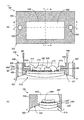
- Fig. 2 is a diagram for explaining a semiconductor device according to the second embodiment.
- Fig. 2(A) is a plan view showing the back of a semiconductor device 100 (the side to which a heat dissipation fin is installed), Fig. 2(B) a cross-sectional diagram of the semiconductor device 100, taken along a dashed line X-X of Fig. 2(A), and Fig. 2(C) a cross-sectional diagram of the semiconductor device 100, taken along a dashed line Y-Y of Fig. 2 (A) .
- the semiconductor device 100 has a plurality of semiconductor elements 200, a circuit board 300 on which the plurality of semiconductor elements 200 are placed, and an aluminum base substrate 400 placed on the circuit board 300.
- the circuit board 300 is configured by an insulating substrate 310 and a circuit layer 320 on the insulating substrate 310, which is a circuit pattern formed from a metal foil piece made of copper or the like.
- the semiconductor device 100 also has a resin case 500 having a storage region 510 with a concave principal surface 511 and an opening 540 and having external terminals 560 formed above the storage region 510.
- the principal surface 511 of the resin case 500 is depressed inward into the shape of a funnel or a ball. Note that illustration of the external terminals 560 is omitted in Fig. 2(C) .
- the resin case 500 is composed of, for example, glass-reinforced epoxy resin or PPS (polyphenylene sulfide) resin.
- screw holes 530 are formed between a rim portion 520 of the resin case 500 and the opening 540. The screw holes 530 are formed facing each other with the opening 540 therebetween.
- the diameter of the screw holes 530 is greater than that of screws 700. It is desired that each screw hole 530 be shaped into a rectangle or an oval that is elongated in the direction connecting the two screw holes 530 (the direction of the dashed line X-X). The number of the screw holes 530 does not have to be two; thus, three or more of the screw holes 530 may be formed, if need be.
- the circuit board 300 is stored in the storage region 510 with the base substrate 400 positioned downward in the diagram.
- the semiconductor elements 200 and the circuit layer 320 on the circuit board 300 stored as described above are electrically connected to the external terminals 560 of the resin case 500 by aluminum wires 210 and sealed with sealing resin 550.
- Soft gel-type resin for example, can be employed as the sealing resin 550.
- a lid with high hardness such as epoxy resin needs to be used to cover the gel-type resin.
- resin with high hardness that consists mainly of epoxy resin can be casted.
- the base substrate 400 has a shape that is pointed downward in the diagram (into the shape of a mound), with its bottom portion (apex portion) being convexed downward, as shown in Figs. 2(B) and 2(C) .
- the level of the apex portion of the base substrate 400 is set in such a manner that the apex portion is accommodated completely in the concave storage region 510 of the resin case 500.
- Fig. 3 is a diagram for explaining a method for installing a heat dissipation fin to the semiconductor device according to the second embodiment.
- Fig. 3(A) shows how the heat dissipation fin 800 is installed to the semiconductor device 100 according to the second embodiment
- Fig. 3(B) shows how the heat dissipation fin 800 is installed to a semiconductor device 100a. Illustration of a heat conductive material to be disposed between the base substrate 400 and the heat dissipation fin 800 is omitted in Fig. 3 .
- a predetermined amount of heat conductive grease (not shown) is disposed as the heat conductive material at substantially the central region on the fixing side of the semiconductor device 100 near the heat dissipation fin 800, and then the semiconductor device 100 is placed on the heat dissipation fin 800 in such a manner that the base substrate 400 faces the heat conductive grease.
- the screws 700 are inserted into the screw holes 530 of the resin case 500 of the semiconductor device 100 and screwed to the heat dissipation fin 800, to fasten the semiconductor device 100 to the heat dissipation fin 800 ( Fig. 3(A) ).
- the heat conductive grease in the vicinity of the center thereof between the base substrate 400 and the heat dissipation fin 800 can be applied with pressure greater than that applied to the periphery. Therefore, the thickness of the heat conductive grease corresponding to the region below the center of the base substrate 400 can be further reduced, and the heat conductive grease can be spread outward. Owing to the rim portion 520 of the storage region 510, the spread heat conductive grease can fill up the storage region 510 without leaking to the outside of the storage region 510 and fill the periphery of the base substrate 400.
- the screws 700 can reliably be screwed to the heat dissipation fin 800 even when the target positions for the screws 700 on the heat dissipation fin 800 are misaligned.
- Fig. 3(B) is now used to explain a method for installing the heat dissipation fin to a semiconductor device in which the principal surface 511 of the resin case is not in the concave shape.
- the semiconductor device 100a is configured by providing the circuit board 300 of the semiconductor device 100 to a resin case 1500 that has one of principal surfaces 511a formed flat instead of concave, as shown in Fig. 3(B) .
- the screws 700 are passed through screw holes 1530 of the resin case 1500 to fasten the heat dissipation fin 800 to the semiconductor device 100a.
- the base substrate 400 receives from the heat dissipation fin 800 a force directed upward in the diagram.
- a force that is directed downward in the diagram acts more on the peripheral portion of the base substrate 400 than on the center of the same.
- the pressure that can be applied in a downward direction in the diagram to the heat dissipation fin 800 is greater in the semiconductor device 100 than the semiconductor device 100a.
- a large pressure can be applied to the heat conductive grease below the base substrate 400, and the heat conductive grease can be spread into a thin layer between the base substrate 400 and the heat dissipation fin 800.
- Such a semiconductor device 100 described above has a semiconductor element 200, a circuit board 300 having the semiconductor element 200 placed on one of its principal surfaces (the upper side of the diagram), a base substrate 400 placed on the other principal surface of the circuit board 300 (the lower side of the diagram), and a resin case 500 having a storage region 510 with a concave principal surface 511 and an opening 540 and having screw holes 530.
- the circuit board 300 is stored in the storage region 510 of the resin case 500 with the base substrate 400 protruding from the concave principal surface 511, and the stored circuit board 300 (the other principal surface thereof (the upper side of the diagram)) is sealed together with the semiconductor element 200 with sealing resin 550.
- the base substrate 400 and the heat dissipation fin 800 are fixed to each other by the heat conductive grease therebetween, and the screw members 700 are inserted into the screw holes 530 of the resin case 500 and screwed to the heat dissipation fin 800, to fasten the semiconductor device 100 to the heat dissipation fin 800.
- the heat conductive grease can be spread into a thin layer between the base substrate 400 and the heat dissipation fin 800, improving the heat dissipation between the base substrate 400 and the heat dissipation fin 800.
- the heat conductive grease that is spread outside the base substrate 400 fills the periphery of the base substrate 400.
- shaping the screw holes 530 into a rectangle or an oval can easily make the directions of the force from the storage member 500 to the base substrate 400 in line with each other.
- Fig. 4 is a diagram for explaining a method for producing the semiconductor device according to the second embodiment.
- Fig. 4 (A) is a plan view showing the back of the semiconductor device 100 (the side to which the heat dissipation fin 800 is installed).
- Figs. 4(B) to 4(D) each show the amount of curvature of the resin case 500 of Fig. 4 (A) at a broken line A-A (upper graphs) and the amount of curvature of the base substrate 400 at a two-dot chain line B-B (lower graphs), which are obtained during the production steps.
- the vertical axes represent the amounts of curvature [ ⁇ m]
- the horizontal axes the situations of the resin case 500 along the broken line A-A and the base substrate 400 along the longitudinal direction.
- a resin case 500 measuring approximately 43 mm in width by 26 mm in height by 3.6 mm in thickness, which has screw holes 530 placed at an interval of 36 mm and has already been curved to have a concave principal surface.
- a circuit board 300 (not shown) measuring approximately 30 mm in width by 13 mm in height, on which is placed a base substrate 400, also curved beforehand, and to which a semiconductor element 200 is soldered as, for example, a switching element (not shown).
- the resin case 500 and the circuit board 300 prepared in this manner are combined. In so doing, the base substrate 400 is placed to face the outside toward the storage region 510 of the resin case 500 (to the side where the heat dissipation fin 800 is placed).
- the maximum amount of curvature of the concave resin case 500 (the amount shown by the arrow in the upper graph) is approximately 153 ⁇ m
- the base substrate 400 is also curved in the same direction as the resin case 500 and has the maximum amount of curvature (the amount shown by the arrow in the lower graph) of approximately 23 ⁇ m.
- the circuit board 300 and the resin case 500 that are installed in this manner are bonded to each other with an adhesive.
- epoxy resin, silicone resin or the like can be used as the adhesive.
- the maximum amount of curvature of the resin case 500 is approximately 235 ⁇ m
- the base substrate 400 is also curved in the same direction as the resin case 500 and has the maximum amount of curvature of approximately 30 ⁇ m.
- the circuit board 300 that is stored in and adhered to the storage region 510 of the resin case 500 as described above is sealed together with the semiconductor element 200 and an aluminum wire 210 with sealing resin 550 (see Fig. 2(B) , for example).
- the maximum amount of curvature of the resin case 500 at this moment is approximately 126 ⁇ m, as shown in Fig. 4(D) .
- the base substrate 400 is pressed by the sealing resin 550 against the side to which the heat dissipation fin 800 is installed, is thereby curved in the direction opposite to the direction in which the resin case 500 is curved, and has an amount of curvature of approximately 45 ⁇ m.
- the semiconductor device 100 can easily be produced in which the resin case 500 and the base substrate 400 that are curved in the same direction beforehand are curved in a desired direction during the production steps.
- the resin case 500 and the base substrate 400 that are already curved beforehand are provided with desired curvature in the production steps.
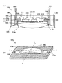
- Fig. 5 is a diagram for explaining another semiconductor device according to the second embodiment.
- Fig. 5(A) is a cross-sectional diagram of a semiconductor device 100b.
- a base substrate 400a is the only difference between the semiconductor device 100b and the semiconductor device 100, as shown in Fig. 5(A) , but the rest of the configuration is the same as that of the semiconductor device 100.
- Fig. 5(B) schematically shows the back of a resin case 500b of the semiconductor device 100c, taken along dashed lines X-X, Y-Y corresponding to those shown in Fig. 2(A) .
- the level of the apex portion of the base substrate 400 is set in such a manner that the apex portion is accommodated completely in the concave storage region 510 of the resin case 500, as described above.
- the base substrate 400a is not completely accommodated in the storage region 510 of the resin case 500, but the level of the apex portion of the base substrate 400a is set such that the apex portion protrudes by approximately several ⁇ m from the storage region 510a.
- the apex portion of the base substrate 400a presses the heat conductive grease at the time when the semiconductor device 100b is placed on the heat dissipation fin 800, with the heat conductive grease therebetween. Thereafter, when fastening the semiconductor device 100b to the heat dissipation fin 800 using the screws 700, the heat conductive grease is constantly pressed by the apex portion of the base substrate 400a and then stably spreads into a thin layer.
- the heat conductive grease can stably be spread into a thin layer by fastening the semiconductor device 100b to the heat dissipation fin 800.
- the base substrate 400 of the semiconductor device 100 is convexed into a mound shape
- the base substrate 400 does not have to be shaped into a mound as long as it is convexed.
- the cross section taken along the dashed line X-X may be in a U-shape
- the cross section taken along the dashed line Y-Y may be in a rectangular shape (so-called semi-cylindrical shape).
- Screw holes 530b in this case are preferably shaped into a rectangle or an oval that is elongated in the direction of the dashed line X-X. Note that Fig. 5(B) shows rectangular screw holes 530b.
- the heat dissipation fin 800 moves along an outer surface of the base substrate 400a. Shaping the screw holes 530b into rectangles, therefore, can securely screw the screws 700 to the moving heat dissipation fin 800.
- the basic shape of the screw holes 530b is a circle with a diameter of 3.5 mm, which is greater than the diameter of the screws 700 by approximately 0.5 mm, so that the heat dissipation fin 800 can be fastened, the screws 700 having a dimensional tolerance of approximately ⁇ 0.3 mm and being of M3 standard.
- the screw holes 530b be shape into an oval that is wider by approximately ⁇ 0.5 mm in the pitch direction.
- the force directed downward in the diagram acts downward from the convex base substrates 400a, 400b onto the heat dissipation fin 800, with the rim portion 520 of the storage regions 510, 510a as a fulcrum with respect to the heat dissipation fin 800, as with the embodiments described above.
- the heat conductive grease can be spread into a thinner layer between each of the base substrates 400a, 400b and the heat dissipation fin 800, improving the heat dissipation between each of the base substrates 400a, 400b and the heat dissipation fin 800.
- the heat conductive grease spread to the outside of the base substrates 400a, 400b fills the peripheries of the base substrates 400a, 400b. This leads to an increase in air tightness of the peripheries of the base substrates 400a, 400b, inhibiting bubbles and the like from being mixed therein and preventing the deterioration of the heat dissipation.
- the heat dissipation of each of the semiconductor devices 100b, 100c to which the heat dissipation fin 800 is installed in this manner can be improved.
- a circuit layer formed from a metal foil piece may be formed on either side of the insulating substrate 310 of the circuit board 300, wherein a semiconductor element 200 may be bonded to one of the circuit layers, and a metal substrate may be bonded to the other circuit layer.
Landscapes
- Cooling Or The Like Of Semiconductors Or Solid State Devices (AREA)
- Cooling Or The Like Of Electrical Apparatus (AREA)
- Engineering & Computer Science (AREA)
- Chemical & Material Sciences (AREA)
- Ceramic Engineering (AREA)
- Materials Engineering (AREA)
- Microelectronics & Electronic Packaging (AREA)
Abstract
Description
- The present invention relates to a semiconductor device, a method for installing a heat dissipation member to the semiconductor device, and a method for producing the semiconductor device.
- A semiconductor module (semiconductor device) such as a power conversion element mounted with a power semiconductor chip has a heat dissipation member such as a heat dissipation fin placed on a metal substrate of the semiconductor module, so that heat generated from the semiconductor chip is released by the heat dissipation member (see Patent Document 1, for example). Such a configuration can prevent the increase of the temperature of the semiconductor module.
- A heat conductive material such as heat conductive grease is applied to the heat dissipation fin or the metal substrate of the semiconductor module prior to placing the heat dissipation fin on the semiconductor module. The heat conductive material is composed of an organic substance, and heat dissipation of the heat conductive material weakens as the coating thickness of the material becomes excessive. For this reason, the heat conductive material needs to be applied in a layer as thin as possible. By fastening the heat dissipation fin to the metal substrate of the semiconductor module with a screw or the like after the application of the heat conductive material, a force to reduce the thickness of the heat conductive material can be generated at the center of the heat dissipation fin immediately below the semiconductor element. As a result, the distance between the metal substrate and the heat dissipation fin decreases, thereby spreading the heat conductive material into a thin layer, further improving the ability to release heat generated from the semiconductor element (see Patent Document 2, for example).
- In addition to using the technology disclosed in Patent Document 2 in which the thickness of the heat conductive material is reduced by changing the shape of the metal substrate (metal base) in the thickness direction, application of a heat conductive material is possible by controlling the shape and thickness of a metal substrate using a metal mask.
- Patent Document 1: Japanese Patent Application Publication No.
2004-363521 - Patent Document 2: Japanese Patent Application Publication No.
2000-058727 - Patent Document 2, however, needs to form projections, mounting holes, and the like on the metal base in order to change the shape of the metal base in the thickness direction, and needs to prepare a mask even when using a metal mask. Forming projections, mounting holes and the like and preparing a mask as described above involve a lot of effort, and thus lead to an increase in production cost.
- The present invention was contrived in view of such circumstances, and an object thereof is to provide a semiconductor device having a configuration different from those described in the foregoing patent documents and thus having improved heat dissipation, a method for installing a heat dissipation member to such a semiconductor device, and a method for producing such a semiconductor device.
- In order to achieve this object, the present invention provides a semiconductor device which has a semiconductor element and on which a heat dissipation member is to be placed, the semiconductor device comprising: a circuit board having the semiconductor element placed on one of principal surfaces thereof; a metal substrate placed on the other principal surface of the circuit board; and a storage member that has a storage region having a concave principal surface and an opening which is disposed on the inside of the concave principal surface to store the circuit board therein with the metal substrate protruding from the concave principal surface, and screw holes that are opened in the concave principal surface to allow passage of screw members that are screwed to the heat dissipation member which is placed in such a manner as to face the metal substrate of the stored circuit board with a heat conductive material therebetween.
- In order to achieve this object, the present invention provides a method for installing a heat dissipation member to such a semiconductor device, and a method for producing such a semiconductor device.
- According to this semiconductor device, the method for installing a heat dissipation member to the semiconductor device, and the method for producing the semiconductor device, heat dissipation of the semiconductor device can be improved.
- The above and other objects, features, and advantages of the present invention will become apparent from the following description associated with the accompanying drawings which illustrate the embodiments preferred as examples of the present invention.
-
-
Fig. 1 is a diagram for explaining a semiconductor device according to a first embodiment and a method for installing a heat dissipation member to the semiconductor device; -
Fig. 2 is a diagram for explaining a semiconductor device according to a second embodiment; -
Fig. 3 is a diagram for explaining a method for installing a heat dissipation fin to the semiconductor device according to the second embodiment; -
Fig. 4 is a diagram for explaining a method for producing the semiconductor device according to the second embodiment; and -
Fig. 5 is a diagram for explaining another semiconductor device according to the second embodiment. - The embodiments of the present invention are now described hereinafter with reference to the drawings.
-
Fig. 1 is a diagram for explaining a semiconductor device according to a first embodiment and a method for installing a heat dissipation member to the semiconductor device. - A
semiconductor device 10 has asemiconductor element 20. Thesemiconductor device 10 is placed on aheat dissipation member 80 and used. When placing thesemiconductor device 10 on theheat dissipation member 80, a heatconductive material 81 is spread evenly into a thin layer between ametal substrate 40 below thesemiconductor element 20 and theheat dissipation member 80. Owing to such a configuration of thesemiconductor device 10, heat of thesemiconductor element 20 can be transmitted from themetal substrate 40 to theheat dissipation member 80, improving the thermal conductivity of thesemiconductor device 10. - As shown in
Fig. 1(A) , thissemiconductor device 10 has acircuit board 30 having thesemiconductor element 20 placed on one of its principal surfaces, and themetal substrate 40 placed on the other principal surface of thecircuit board 30. - The
semiconductor device 10 also has astorage member 50 for accommodating thecircuit board 30. Thestorage member 50 is a frame-like (O-shaped) or rim-like member and has astorage region 51 having a concaveprincipal surface 51a (the lower side of the diagram) and anopening 54 disposed on the inside of thisconcave principal surface 51a. Thestorage member 50 further hasscrew holes 53 passing between the concaveprincipal surface 51a and a principal surface facing theprincipal surface 51a (the upper side of the diagram). Thecircuit board 30 is stored in theopening 54, with themetal substrate 40 protruding from the concave principal surface. Screw members 70 (described hereinafter) are inserted into thescrew holes 53 and screwed to theheat dissipation member 80 that is placed facing themetal substrate 40 of thestored circuit board 30 with the heatconductive material 81 therebetween. The concaveprincipal surface 51a is configured by a flat surface or a curved surface that is inclined with respect to the principal surface facing theprincipal surface 51a (the upper side of the diagram), and is formed in such a manner that arim portion 52 disposed outside thescrew holes 53 in thestorage region 51 protrudes toward theheat dissipation member 80. Thescrew holes 53 are formed, with the axes thereof situated substantially perpendicular to the upper surface of thestorage member 50. Note that thecircuit board 30, which is stored in thestorage region 51 of thestorage member 50, is sealed together with thesemiconductor element 20 withresin 55. - Next is described a method for installing the
semiconductor device 10 of such a configuration to theheat dissipation member 80. - First, a predetermined amount of the heat
conductive material 81 is disposed in a region of theheat dissipation member 80 with which themetal substrate 40 comes into contact (Fig. 1(A) ). Note that the heatconductive material 81 may be disposed in the region near themetal substrate 40. The heatconductive material 81 is heat conductive grease (a thermal compound) or the like that is generally used. - The
heat dissipation member 80 with the heatconductive material 81 and thesemiconductor device 10 are then fixed to each other. In so doing, theheat dissipation member 80 is supported by therim portion 52 of thestorage region 51 of thestorage member 50 of thesemiconductor device 10. The heatconductive material 81 is spread between theheat dissipation member 80 and themetal substrate 40 of the semiconductor device 10 (Fig. 1(B) ). - The
screw members 70 are inserted into thescrew holes 53 of thestorage member 50 of thesemiconductor device 10 and screwed to theheat dissipation member 80, to fasten thesemiconductor device 10 to the heat dissipation member 80 (Fig. 1(C) ). - In the
semiconductor device 10 at this moment, a force is applied to the center of themetal substrate 40, with therim portion 52 of thestorage region 51 as a fulcrum with respect to theheat dissipation member 80, and a force that is directed downward in the diagram acts from themetal substrate 40 onto theheat dissipation member 80. The heatconductive material 81 can be spread into a thin layer as the distance between themetal substrate 40 and theheat dissipation member 80 decreases as described above. As a result, heat dissipation between themetal substrate 40 and theheat dissipation member 80 improves. Moreover, the heatconductive material 81 spreads outside themetal substrate 40 and fills the periphery of themetal substrate 40. This leads to an increase in air tightness of the periphery of themetal substrate 40, inhibiting bubbles and the like from being mixed therein and preventing the deterioration of the heat dissipation. - The
semiconductor device 10 described above has thesemiconductor element 20, thecircuit board 30 having thesemiconductor element 20 placed on one of its principal surfaces, themetal substrate 40 placed on the other principal surface of thecircuit board 30, and thestorage member 50 that has thestorage region 51 in which theprincipal surface 51a thereof configures a concave opening, and thescrew holes 53. In thesemiconductor device 10, thecircuit board 30 is stored in thestorage region 51 of thestorage member 50, with themetal substrate 40 protruding from theconcave principal surface 51a, and thestored circuit board 30 is sealed together with thesemiconductor element 20 with theresin 55. Themetal substrate 40 and theheat dissipation member 80 are fixed to each other by the heatconductive material 81 therebetween, and thescrew members 70 are inserted into thescrew holes 53 of thestorage member 50 and screwed to theheat dissipation member 80, to fasten thesemiconductor device 10 to theheat dissipation member 80. - By fastening the
semiconductor device 10 to theheat dissipation member 80 as described above, a force from thestorage member 50 is applied to the center of themetal substrate 40 in thesemiconductor device 10, with therim portion 52 of thestorage region 51 as a fulcrum, and a force that is directed downward in the diagram acts from themetal substrate 40 onto theheat dissipation member 80. As a result, the heatconductive material 81 can be spread into a thin layer between themetal substrate 40 and theheat dissipation member 80, improving the heat dissipation between themetal substrate 40 and theheat dissipation member 80. Moreover, the heatconductive material 81 that is spread to the outside of themetal substrate 40 fills the periphery of themetal substrate 40. This leads to an increase in air tightness of the periphery of themetal substrate 40, inhibiting bubbles and the like from being mixed therein and preventing the deterioration of the heat dissipation. Heat dissipation of thesemiconductor device 10 to which theheat dissipation member 80 is installed in this manner can be improved. - In the second embodiment, the semiconductor device of the first embodiment is described with more specific examples.
-
Fig. 2 is a diagram for explaining a semiconductor device according to the second embodiment. -
Fig. 2(A) is a plan view showing the back of a semiconductor device 100 (the side to which a heat dissipation fin is installed),Fig. 2(B) a cross-sectional diagram of thesemiconductor device 100, taken along a dashed line X-X ofFig. 2(A), and Fig. 2(C) a cross-sectional diagram of thesemiconductor device 100, taken along a dashed line Y-Y ofFig. 2 (A) . - The
semiconductor device 100 has a plurality ofsemiconductor elements 200, acircuit board 300 on which the plurality ofsemiconductor elements 200 are placed, and analuminum base substrate 400 placed on thecircuit board 300. - The
circuit board 300 is configured by an insulatingsubstrate 310 and acircuit layer 320 on the insulatingsubstrate 310, which is a circuit pattern formed from a metal foil piece made of copper or the like. - The
semiconductor device 100 also has aresin case 500 having astorage region 510 with a concaveprincipal surface 511 and anopening 540 and havingexternal terminals 560 formed above thestorage region 510. Theprincipal surface 511 of theresin case 500 is depressed inward into the shape of a funnel or a ball. Note that illustration of theexternal terminals 560 is omitted inFig. 2(C) . Theresin case 500 is composed of, for example, glass-reinforced epoxy resin or PPS (polyphenylene sulfide) resin. In addition, screw holes 530 are formed between arim portion 520 of theresin case 500 and theopening 540. The screw holes 530 are formed facing each other with theopening 540 therebetween. The diameter of the screw holes 530 is greater than that ofscrews 700. It is desired that eachscrew hole 530 be shaped into a rectangle or an oval that is elongated in the direction connecting the two screw holes 530 (the direction of the dashed line X-X). The number of the screw holes 530 does not have to be two; thus, three or more of the screw holes 530 may be formed, if need be. In thisresin case 500, thecircuit board 300 is stored in thestorage region 510 with thebase substrate 400 positioned downward in the diagram. Thesemiconductor elements 200 and thecircuit layer 320 on thecircuit board 300 stored as described above are electrically connected to theexternal terminals 560 of theresin case 500 byaluminum wires 210 and sealed with sealingresin 550. Soft gel-type resin, for example, can be employed as the sealingresin 550. When using gel-type resin as the sealingresin 550, a lid with high hardness such as epoxy resin needs to be used to cover the gel-type resin. When sealing with the sealingresin 550, resin with high hardness that consists mainly of epoxy resin can be casted. - Note that the
base substrate 400 has a shape that is pointed downward in the diagram (into the shape of a mound), with its bottom portion (apex portion) being convexed downward, as shown inFigs. 2(B) and 2(C) . For this reason, the level of the apex portion of thebase substrate 400 is set in such a manner that the apex portion is accommodated completely in theconcave storage region 510 of theresin case 500. - A method for installing a
heat dissipation fin 800 to such asemiconductor device 100 is now described with reference toFig. 3 . -
Fig. 3 is a diagram for explaining a method for installing a heat dissipation fin to the semiconductor device according to the second embodiment. - Note that
Fig. 3(A) shows how theheat dissipation fin 800 is installed to thesemiconductor device 100 according to the second embodiment, whileFig. 3(B) shows how theheat dissipation fin 800 is installed to asemiconductor device 100a. Illustration of a heat conductive material to be disposed between thebase substrate 400 and theheat dissipation fin 800 is omitted inFig. 3 . - First of all, a predetermined amount of heat conductive grease (not shown) is disposed as the heat conductive material at substantially the central region on the fixing side of the
semiconductor device 100 near theheat dissipation fin 800, and then thesemiconductor device 100 is placed on theheat dissipation fin 800 in such a manner that thebase substrate 400 faces the heat conductive grease. - The
screws 700 are inserted into the screw holes 530 of theresin case 500 of thesemiconductor device 100 and screwed to theheat dissipation fin 800, to fasten thesemiconductor device 100 to the heat dissipation fin 800 (Fig. 3(A) ). - In so doing, in the
semiconductor device 100, when a force that is directed downward in the diagram is applied by thescrews 700 screwed to theheat dissipation fin 800, the force acts on the center of thebase substrate 400, with therim portion 520 of thestorage region 510 supporting theheat dissipation fin 800 as a fulcrum. Consequently, a force that is directed downward in the diagram acts from thebase substrate 400 onto theheat dissipation fin 800. - In addition, due to the downwardly-convexed shape of the bottom portion (apex portion) of the
base substrate 400 of thesemiconductor device 100, the heat conductive grease (in the vicinity of the center thereof) between thebase substrate 400 and theheat dissipation fin 800 can be applied with pressure greater than that applied to the periphery. Therefore, the thickness of the heat conductive grease corresponding to the region below the center of thebase substrate 400 can be further reduced, and the heat conductive grease can be spread outward. Owing to therim portion 520 of thestorage region 510, the spread heat conductive grease can fill up thestorage region 510 without leaking to the outside of thestorage region 510 and fill the periphery of thebase substrate 400. - When fastening the
semiconductor device 100 to theheat dissipation fin 800 using thescrews 700, because the diameter of the screw holes 530 is greater than that of thescrews 700, thescrews 700 can reliably be screwed to theheat dissipation fin 800 even when the target positions for thescrews 700 on theheat dissipation fin 800 are misaligned. - For comparison of the installation of the
heat dissipation fin 800 to thesemiconductor device 100,Fig. 3(B) is now used to explain a method for installing the heat dissipation fin to a semiconductor device in which theprincipal surface 511 of the resin case is not in the concave shape. - The
semiconductor device 100a is configured by providing thecircuit board 300 of thesemiconductor device 100 to aresin case 1500 that has one ofprincipal surfaces 511a formed flat instead of concave, as shown inFig. 3(B) . - As with the configuration of the
semiconductor device 100, thescrews 700 are passed throughscrew holes 1530 of theresin case 1500 to fasten theheat dissipation fin 800 to thesemiconductor device 100a. In this case, while thesemiconductor device 100a receives from the screws 700 a force directed downward in the diagram, thebase substrate 400 receives from the heat dissipation fin 800 a force directed upward in the diagram. In thesemiconductor device 100a, therefore, a force that is directed downward in the diagram acts more on the peripheral portion of thebase substrate 400 than on the center of the same. - For this reason, the pressure that can be applied in a downward direction in the diagram to the
heat dissipation fin 800 is greater in thesemiconductor device 100 than thesemiconductor device 100a. Thus, in thesemiconductor device 100, a large pressure can be applied to the heat conductive grease below thebase substrate 400, and the heat conductive grease can be spread into a thin layer between thebase substrate 400 and theheat dissipation fin 800. - Such a
semiconductor device 100 described above has asemiconductor element 200, acircuit board 300 having thesemiconductor element 200 placed on one of its principal surfaces (the upper side of the diagram), abase substrate 400 placed on the other principal surface of the circuit board 300 (the lower side of the diagram), and aresin case 500 having astorage region 510 with a concaveprincipal surface 511 and anopening 540 and having screw holes 530. In thesemiconductor device 100, thecircuit board 300 is stored in thestorage region 510 of theresin case 500 with thebase substrate 400 protruding from the concaveprincipal surface 511, and the stored circuit board 300 (the other principal surface thereof (the upper side of the diagram)) is sealed together with thesemiconductor element 200 with sealingresin 550. Thebase substrate 400 and theheat dissipation fin 800 are fixed to each other by the heat conductive grease therebetween, and thescrew members 700 are inserted into the screw holes 530 of theresin case 500 and screwed to theheat dissipation fin 800, to fasten thesemiconductor device 100 to theheat dissipation fin 800. - By fastening the
semiconductor device 100 to theheat dissipation fin 800 as described above, a force from thestorage member 500 is applied to the center of thebase substrate 400 in thesemiconductor device 100, with therim portion 520 of thestorage region 510 as a fulcrum, and a force that is directed downward in the diagram acts from theconvex base substrate 400 onto theheat dissipation fin 800. As a result, the heat conductive grease can be spread into a thin layer between thebase substrate 400 and theheat dissipation fin 800, improving the heat dissipation between thebase substrate 400 and theheat dissipation fin 800. Moreover, the heat conductive grease that is spread outside thebase substrate 400 fills the periphery of thebase substrate 400. This leads to an increase in air tightness of the periphery of thebase substrate 400, inhibiting bubbles and the like from being mixed therein and preventing the deterioration of the heat dissipation. Heat dissipation of thesemiconductor device 100 to which theheat dissipation fin 800 is installed in this manner can be improved. - In addition, shaping the screw holes 530 into a rectangle or an oval can easily make the directions of the force from the
storage member 500 to thebase substrate 400 in line with each other. - A method for producing this
semiconductor device 100 is described next with reference toFig. 4 . -
Fig. 4 is a diagram for explaining a method for producing the semiconductor device according to the second embodiment. - Note that
Fig. 4 (A) is a plan view showing the back of the semiconductor device 100 (the side to which theheat dissipation fin 800 is installed).Figs. 4(B) to 4(D) each show the amount of curvature of theresin case 500 ofFig. 4 (A) at a broken line A-A (upper graphs) and the amount of curvature of thebase substrate 400 at a two-dot chain line B-B (lower graphs), which are obtained during the production steps. In each ofFigs. 4(B) to 4(D) , the vertical axes represent the amounts of curvature [µm], and the horizontal axes the situations of theresin case 500 along the broken line A-A and thebase substrate 400 along the longitudinal direction. - First, prepared is a
resin case 500 measuring approximately 43 mm in width by 26 mm in height by 3.6 mm in thickness, which hasscrew holes 530 placed at an interval of 36 mm and has already been curved to have a concave principal surface. Next prepared is a circuit board 300 (not shown) measuring approximately 30 mm in width by 13 mm in height, on which is placed abase substrate 400, also curved beforehand, and to which asemiconductor element 200 is soldered as, for example, a switching element (not shown). Theresin case 500 and thecircuit board 300 prepared in this manner are combined. In so doing, thebase substrate 400 is placed to face the outside toward thestorage region 510 of the resin case 500 (to the side where theheat dissipation fin 800 is placed). - In this case, as shown in
Fig. 4(B) , the maximum amount of curvature of the concave resin case 500 (the amount shown by the arrow in the upper graph) is approximately 153 µm, and thebase substrate 400 is also curved in the same direction as theresin case 500 and has the maximum amount of curvature (the amount shown by the arrow in the lower graph) of approximately 23 µm. - Subsequently, the
circuit board 300 and theresin case 500 that are installed in this manner are bonded to each other with an adhesive. Note that epoxy resin, silicone resin or the like can be used as the adhesive. In this case, as shown inFig. 4(C) , the maximum amount of curvature of theresin case 500 is approximately 235 µm, and thebase substrate 400 is also curved in the same direction as theresin case 500 and has the maximum amount of curvature of approximately 30 µm. - The
circuit board 300 that is stored in and adhered to thestorage region 510 of theresin case 500 as described above is sealed together with thesemiconductor element 200 and analuminum wire 210 with sealing resin 550 (seeFig. 2(B) , for example). The maximum amount of curvature of theresin case 500 at this moment is approximately 126 µm, as shown inFig. 4(D) . Thebase substrate 400, on the other hand, is pressed by the sealingresin 550 against the side to which theheat dissipation fin 800 is installed, is thereby curved in the direction opposite to the direction in which theresin case 500 is curved, and has an amount of curvature of approximately 45 µm. - The
semiconductor device 100 can easily be produced in which theresin case 500 and thebase substrate 400 that are curved in the same direction beforehand are curved in a desired direction during the production steps. - In the foregoing method for producing the
semiconductor device 100, theresin case 500 and thebase substrate 400 that are already curved beforehand are provided with desired curvature in the production steps. In addition to such process, it is also possible to form a concave storage region in theresin case 500 and to form thebase substrate 400 into a convex shape, and then theresultant base substrate 400 can be placed on theresultant resin case 500 to produce thesemiconductor device 100. - Next, various aspects of the semiconductor device are described with reference to
Fig. 5 . -
Fig. 5 is a diagram for explaining another semiconductor device according to the second embodiment. - Note that
Fig. 5(A) is a cross-sectional diagram of asemiconductor device 100b. Abase substrate 400a is the only difference between thesemiconductor device 100b and thesemiconductor device 100, as shown inFig. 5(A) , but the rest of the configuration is the same as that of thesemiconductor device 100.Fig. 5(B) schematically shows the back of aresin case 500b of thesemiconductor device 100c, taken along dashed lines X-X, Y-Y corresponding to those shown inFig. 2(A) . - In the
semiconductor device 100, the level of the apex portion of thebase substrate 400 is set in such a manner that the apex portion is accommodated completely in theconcave storage region 510 of theresin case 500, as described above. - In the
semiconductor device 100b, on the other hand, thebase substrate 400a is not completely accommodated in thestorage region 510 of theresin case 500, but the level of the apex portion of thebase substrate 400a is set such that the apex portion protrudes by approximately several µm from thestorage region 510a. - As a result of configuring the
base substrate 400a into this size, the apex portion of thebase substrate 400a presses the heat conductive grease at the time when thesemiconductor device 100b is placed on theheat dissipation fin 800, with the heat conductive grease therebetween. Thereafter, when fastening thesemiconductor device 100b to theheat dissipation fin 800 using thescrews 700, the heat conductive grease is constantly pressed by the apex portion of thebase substrate 400a and then stably spreads into a thin layer. - Due to the configuration of the
base substrate 400a in which the apex portion thereof protrudes by approximately several µm from thestorage region 510a, the heat conductive grease can stably be spread into a thin layer by fastening thesemiconductor device 100b to theheat dissipation fin 800. - Although the
base substrate 400 of thesemiconductor device 100 is convexed into a mound shape, thebase substrate 400 does not have to be shaped into a mound as long as it is convexed. Thus, as shown inFig. 5(B) , for example, the cross section taken along the dashed line X-X may be in a U-shape, and the cross section taken along the dashed line Y-Y may be in a rectangular shape (so-called semi-cylindrical shape). - Screw holes 530b in this case are preferably shaped into a rectangle or an oval that is elongated in the direction of the dashed line X-X. Note that
Fig. 5(B) shows rectangular screw holes 530b. When fastening theheat dissipation fin 800 to thesemiconductor device 100c, there is a possibility that theheat dissipation fin 800 moves along an outer surface of thebase substrate 400a. Shaping the screw holes 530b into rectangles, therefore, can securely screw thescrews 700 to the movingheat dissipation fin 800. For instance, the basic shape of thescrew holes 530b is a circle with a diameter of 3.5 mm, which is greater than the diameter of thescrews 700 by approximately 0.5 mm, so that theheat dissipation fin 800 can be fastened, thescrews 700 having a dimensional tolerance of approximately ±0.3 mm and being of M3 standard. Moreover, in view of the pitch difference of approximately ±0.3 mm between the screw holes 350b, it is preferred that the screw holes 530b be shape into an oval that is wider by approximately ±0.5 mm in the pitch direction. - In the situation shown in
Fig. 5 as well, in thesemiconductor devices heat dissipation fin 800 with thescrews 700, the force directed downward in the diagram acts downward from theconvex base substrates heat dissipation fin 800, with therim portion 520 of thestorage regions heat dissipation fin 800, as with the embodiments described above. As a result, the heat conductive grease can be spread into a thinner layer between each of thebase substrates heat dissipation fin 800, improving the heat dissipation between each of thebase substrates heat dissipation fin 800. In addition, the heat conductive grease spread to the outside of thebase substrates base substrates base substrates semiconductor devices heat dissipation fin 800 is installed in this manner can be improved. - It should be noted that the embodiments described above are to illustrate the specific examples of the present invention. Therefore, the present invention should not be construed as being limited to these embodiments, and various modifications can be made to the present invention without departing from the gist thereof. For example, a circuit layer formed from a metal foil piece (not shown) may be formed on either side of the insulating
substrate 310 of thecircuit board 300, wherein asemiconductor element 200 may be bonded to one of the circuit layers, and a metal substrate may be bonded to the other circuit layer. - The above description merely illustrates the principles of the present invention. A person skilled in the art can make various modifications and changes; thus, the present invention is not limited to the precise configurations and applications illustrated and described above. Therefore, all suitable modifications and equivalents are deemed to fall within the scope of the present invention defined by the appended claims and equivalents thereof.
-
- 10
- Semiconductor device
- 20
- Semiconductor element
- 30
- Circuit board
- 40
- Metal substrate
- 50
- Storage member
- 51
- Storage region
- 51a
- Principal surface
- 52
- Rim portion
- 53
- Screw hole
- 54
- Opening
- 55
- Resin
- 70
- Screw member
- 80
- Heat dissipation member
- 81
- Heat conductive material
Claims (10)
- A semiconductor device which has a semiconductor element and on which a heat dissipation member is to be placed, the semiconductor device comprising:a circuit board having the semiconductor element placed on one of principal surfaces thereof;a metal substrate placed on the other principal surface of the circuit board; anda storage member that has a storage region having a concave principal surface and an opening which is disposed on the inside of the concave principal surface to store the circuit board therein with the metal substrate protruding from the concave principal surface, and screw holes that are opened in the concave principal surface to allow passage of screw members that are screwed to the heat dissipation member which is placed in such a manner as to face the metal substrate of the stored circuit board with a heat conductive material therebetween.
- The semiconductor device according to claim 1, wherein the concave principal surface is formed in such a manner that the storage region outside the screw holes protrudes toward the heat dissipation member.
- The semiconductor device according to claim 2, wherein the screw holes are formed facing each other in the storage member, with the metal substrate of the stored circuit board therebetween.
- The semiconductor device according to claim 1, wherein the metal substrate has a convex surface that faces the heat dissipation member to be placed.
- The semiconductor device according to claim 4, wherein the metal substrate is in the shape of a mound.
- The semiconductor device according to claim 4, wherein the metal substrate is in a semi-cylindrical shape.
- The semiconductor device according to claim 6, wherein the screw holes are shaped into an oval or a rectangle in a radial direction and formed as a pair such that major axes thereof are in line with each other with the metal substrate of the stored circuit board therebetween.
- The semiconductor device according to claim 1, wherein the circuit board stored in the storage region of the storage member is sealed together with the semiconductor element placed on the circuit board with resin, from a principal surface of the circuit board on a side opposite to the principal surface.
- A method for installing a heat dissipation member to a semiconductor device having a semiconductor element,
the semiconductor device including:a circuit board having the semiconductor element placed on one of principal surfaces thereof;a metal substrate placed on the other principal surface of the circuit board; anda storage member that has a storage region having a concave principal surface and an opening which is disposed on the inside of the concave principal surface to store the circuit board therein with the metal substrate protruding from the concave principal surface, and screw holes that are opened in the concave principal surface to allow passage of screw members, andthe method comprising the steps of:placing the heat dissipation member on the storage member with a heat conductive material therebetween so that the heat dissipation member faces the metal substrate of the circuit board stored in the storage region of the storage member;inserting the screw members into the screw holes; and screwing the heat dissipation member to the storage member. - A method for producing a semiconductor device which has a semiconductor element and on which a heat dissipation member is to be placed, the method comprising the steps of:storing a circuit board in a storage region that has a concave principal surface and an opening and is provided in a storage member having screw holes allowing passage of screw members, the circuit board being curved into a concave shape in the same direction as the storage member, having the semiconductor element placed on one of principal surfaces thereof, having a metal substrate disposed on the other principal surface, and being stored in the storage region with the metal substrate protruding from the concave principal surface;sealing, with resin, the semiconductor element on the circuit board stored in the storage region of the storage member; andcurving the circuit board in a direction opposite to the direction of curvature of the storage member.
Applications Claiming Priority (2)
| Application Number | Priority Date | Filing Date | Title |
|---|---|---|---|
| JP2012201775 | 2012-09-13 | ||
| PCT/JP2013/071785 WO2014041936A1 (en) | 2012-09-13 | 2013-08-12 | Semiconductor device, method for attaching heat dissipating member to semiconductor device, and method for manufacturing semiconductor device |
Publications (3)
| Publication Number | Publication Date |
|---|---|
| EP2814056A1 true EP2814056A1 (en) | 2014-12-17 |
| EP2814056A4 EP2814056A4 (en) | 2015-10-28 |
| EP2814056B1 EP2814056B1 (en) | 2017-07-12 |
Family
ID=50278061
Family Applications (1)
| Application Number | Title | Priority Date | Filing Date |
|---|---|---|---|
| EP13837550.6A Active EP2814056B1 (en) | 2012-09-13 | 2013-08-12 | Semiconductor device, method for attaching heat dissipating member to semiconductor device, and method for manufacturing semiconductor device |
Country Status (6)
| Country | Link |
|---|---|
| US (1) | US9711430B2 (en) |
| EP (1) | EP2814056B1 (en) |
| JP (1) | JP5871076B2 (en) |
| KR (1) | KR20150053874A (en) |
| CN (1) | CN104170079B (en) |
| WO (1) | WO2014041936A1 (en) |
Cited By (2)
| Publication number | Priority date | Publication date | Assignee | Title |
|---|---|---|---|---|
| JP2020198342A (en) * | 2019-05-31 | 2020-12-10 | 三菱電機株式会社 | Semiconductor device |
| EP3872854A1 (en) * | 2020-02-27 | 2021-09-01 | Littelfuse, Inc. | Power module housing with improved protrusion design |
Families Citing this family (34)
| Publication number | Priority date | Publication date | Assignee | Title |
|---|---|---|---|---|
| CN104838493B (en) * | 2012-11-28 | 2017-07-14 | 三菱电机株式会社 | power module |
| US10096566B2 (en) * | 2014-07-09 | 2018-10-09 | Mitsubishi Electric Corporation | Semiconductor device |
| JP6356550B2 (en) * | 2014-09-10 | 2018-07-11 | 三菱電機株式会社 | Semiconductor device and manufacturing method thereof |
| JP6500162B2 (en) * | 2015-03-23 | 2019-04-10 | 広東美的制冷設備有限公司Gd Midea Air−Conditioning Equipment Co.,Ltd. | Intelligent power module and manufacturing method thereof |
| KR101652904B1 (en) | 2016-01-14 | 2016-08-31 | 주식회사 엠디엠 | Multi-layer pcb having function of dissipating heat from power semiconductor module package and pcb, and the producing method thereof |
| KR102543495B1 (en) | 2016-07-06 | 2023-06-13 | 김구용 | PCB module having multi-directional heat-radiation structure, and radiation plate, multi-layer PCB assembly, and module case used in the same PCB module |
| KR102592659B1 (en) | 2016-08-08 | 2023-10-20 | 김구용 | PCB module having multi-directional heat-radiation structure and multi-layer PCB assembly used in the PCB module |
| KR101927088B1 (en) | 2016-08-08 | 2019-03-12 | 김구용 | PCB module having multi-directional heat-radiation structure and multi-layer PCB assembly used in the PCB module |
| KR101896556B1 (en) | 2016-08-30 | 2018-09-10 | 주식회사 엠디엠 | Multi-layer PCB assembly having multi-directional heat-radiation structure |
| JP6724668B2 (en) * | 2016-09-07 | 2020-07-15 | トヨタ自動車株式会社 | Semiconductor device |
| JP6748223B2 (en) * | 2016-11-28 | 2020-08-26 | 京セラ株式会社 | Semiconductor package and semiconductor device |
| CN109564908B (en) * | 2017-02-13 | 2022-06-24 | 富士电机株式会社 | Semiconductor device and method for manufacturing semiconductor device |
| TWI618859B (en) * | 2017-02-20 | 2018-03-21 | 研能科技股份有限公司 | Air cooling heat dissipation device |
| JP2018195717A (en) * | 2017-05-17 | 2018-12-06 | 富士電機株式会社 | Semiconductor module, semiconductor module base plate, and semiconductor device manufacturing method |
| JP6768612B2 (en) * | 2017-09-06 | 2020-10-14 | 三菱電機株式会社 | Semiconductor device |
| JP7056366B2 (en) * | 2018-05-16 | 2022-04-19 | 富士電機株式会社 | Semiconductor modules and semiconductor devices using them |
| JP7234657B2 (en) * | 2018-05-28 | 2023-03-08 | 株式会社デンソー | electronic device |
| JP2018133598A (en) * | 2018-06-05 | 2018-08-23 | 三菱電機株式会社 | Semiconductor device and manufacturing method of the same |
| JP6906654B2 (en) * | 2018-06-05 | 2021-07-21 | 三菱電機株式会社 | Semiconductor devices and their manufacturing methods |
| US11688665B2 (en) | 2018-06-13 | 2023-06-27 | Intel Corporation | Thermal management solutions for stacked integrated circuit devices |
| US11482472B2 (en) * | 2018-06-13 | 2022-10-25 | Intel Corporation | Thermal management solutions for stacked integrated circuit devices |
| US10764996B1 (en) * | 2018-06-19 | 2020-09-01 | Xilinx, Inc. | Chip package assembly with composite stiffener |
| DE112019007029T5 (en) * | 2019-03-15 | 2021-12-02 | Mitsubishi Electric Corporation | Semiconductor device and semiconductor device with cooling member |
| JP7386435B2 (en) * | 2019-03-28 | 2023-11-27 | パナソニックIpマネジメント株式会社 | Wiring board and its manufacturing method |
| JP7354605B2 (en) * | 2019-06-17 | 2023-10-03 | 富士電機株式会社 | Semiconductor modules and semiconductor devices |
| US12046533B2 (en) * | 2019-06-25 | 2024-07-23 | Mitsubishi Electric Corporation | Semiconductor device |
| JP6849137B1 (en) * | 2020-07-06 | 2021-03-24 | 富士電機株式会社 | Semiconductor device |
| JP7378379B2 (en) * | 2020-11-02 | 2023-11-13 | 三菱電機株式会社 | Power semiconductor modules and power conversion devices |
| CN112420636B (en) * | 2020-11-19 | 2022-09-06 | 四川长虹空调有限公司 | Chip heat radiation structure |
| JP7790024B2 (en) * | 2021-03-01 | 2025-12-23 | 富士電機株式会社 | Semiconductor device and manufacturing method thereof |
| JP7751178B2 (en) * | 2021-06-17 | 2025-10-08 | ミネベアパワーデバイス株式会社 | Power Semiconductor Module |
| JP7757699B2 (en) * | 2021-10-12 | 2025-10-22 | 富士電機株式会社 | Semiconductor Module |
| JP7586064B2 (en) * | 2021-12-14 | 2024-11-19 | 株式会社明電舎 | Resin cover mounting structure for electrical equipment |
| JP7394243B1 (en) | 2023-02-02 | 2023-12-07 | 株式会社オリジン | Heating device and method for manufacturing soldered objects |
Family Cites Families (31)
| Publication number | Priority date | Publication date | Assignee | Title |
|---|---|---|---|---|
| DE2712543C2 (en) * | 1976-03-24 | 1982-11-11 | Hitachi, Ltd., Tokyo | Arrangement of a semiconductor component on a mounting plate |
| JPH0496355A (en) | 1990-08-13 | 1992-03-27 | Meidensha Corp | Manufacture of semiconductor device |
| US5172755A (en) * | 1992-04-01 | 1992-12-22 | Digital Equipment Corporation | Arcuate profiled heatsink apparatus and method |
| DE4233073A1 (en) | 1992-10-01 | 1994-04-07 | Siemens Ag | Semiconductor modular structure prodn. - by convexly shaping and bonding in single hot pressing operation |
| DE4338107C1 (en) * | 1993-11-08 | 1995-03-09 | Eupec Gmbh & Co Kg | Semiconductor module |
| JPH07273257A (en) * | 1994-03-29 | 1995-10-20 | Kyocera Corp | Package for storing semiconductor devices |
| JP3316714B2 (en) * | 1994-05-31 | 2002-08-19 | 三菱電機株式会社 | Semiconductor device |
| JP3225457B2 (en) * | 1995-02-28 | 2001-11-05 | 株式会社日立製作所 | Semiconductor device |
| JP3110657B2 (en) * | 1995-08-02 | 2000-11-20 | 松下電子工業株式会社 | Resin-sealed semiconductor device and method of manufacturing the same |
| JP3336910B2 (en) * | 1997-06-09 | 2002-10-21 | 株式会社日立製作所 | Power semiconductor module |
| JPH11177002A (en) | 1997-12-09 | 1999-07-02 | Toyota Motor Corp | Method for manufacturing semiconductor device |
| JP2000058727A (en) | 1998-08-12 | 2000-02-25 | Hitachi Ltd | Power semiconductor module |
| JP3919398B2 (en) * | 1999-10-27 | 2007-05-23 | 三菱電機株式会社 | Semiconductor module |
| JP4015023B2 (en) * | 2001-02-22 | 2007-11-28 | 日本碍子株式会社 | ELECTRONIC CIRCUIT MEMBER, ITS MANUFACTURING METHOD, AND ELECTRONIC COMPONENT |
| JP2003303933A (en) | 2002-04-12 | 2003-10-24 | Toyota Motor Corp | Method for manufacturing semiconductor device |
| KR100488518B1 (en) * | 2002-11-14 | 2005-05-11 | 삼성전자주식회사 | Heat dissipation system for semiconductor device |
| JP3960264B2 (en) | 2003-05-22 | 2007-08-15 | トヨタ自動車株式会社 | Manufacturing method of semiconductor device |
| JP4140452B2 (en) | 2003-06-09 | 2008-08-27 | トヨタ自動車株式会社 | Semiconductor device heat dissipation structure |
| JP2006080153A (en) * | 2004-09-07 | 2006-03-23 | Toshiba Corp | Semiconductor device |
| CN101039566A (en) * | 2006-03-17 | 2007-09-19 | 富准精密工业(深圳)有限公司 | Heat abstractor and electronic device using the same |
| US7479704B2 (en) * | 2007-01-10 | 2009-01-20 | Powertech Technology Inc. | Substrate improving immobilization of ball pads for BGA packages |
| JP5061717B2 (en) * | 2007-05-18 | 2012-10-31 | 富士電機株式会社 | Semiconductor module and method for manufacturing semiconductor module |
| US8154114B2 (en) | 2007-08-06 | 2012-04-10 | Infineon Technologies Ag | Power semiconductor module |
| US8018047B2 (en) * | 2007-08-06 | 2011-09-13 | Infineon Technologies Ag | Power semiconductor module including a multilayer substrate |
| CN101398159A (en) * | 2007-09-24 | 2009-04-01 | 周裕元 | LED lamp |
| US7808100B2 (en) * | 2008-04-21 | 2010-10-05 | Infineon Technologies Ag | Power semiconductor module with pressure element and method for fabricating a power semiconductor module with a pressure element |
| CN101769460A (en) * | 2009-01-07 | 2010-07-07 | 富准精密工业(深圳)有限公司 | Light emitting diode lamp |
| DE102009026558B3 (en) * | 2009-05-28 | 2010-12-02 | Infineon Technologies Ag | Power semiconductor module with movably mounted circuit carriers and method for producing such a power semiconductor module |
| CN101923193A (en) * | 2009-06-17 | 2010-12-22 | 中国科学院微电子研究所 | Pluggable optical transceiver integrated module |
| DE112012005472T5 (en) * | 2011-12-26 | 2014-09-11 | Mitsubishi Electric Corporation | Electric power semiconductor device and method of manufacturing the same |
| WO2013175714A1 (en) | 2012-05-22 | 2013-11-28 | パナソニック株式会社 | Semiconductor device and method for manufacturing same |
-
2013
- 2013-08-12 EP EP13837550.6A patent/EP2814056B1/en active Active
- 2013-08-12 WO PCT/JP2013/071785 patent/WO2014041936A1/en not_active Ceased
- 2013-08-12 CN CN201380014851.5A patent/CN104170079B/en active Active
- 2013-08-12 JP JP2014535454A patent/JP5871076B2/en active Active
- 2013-08-12 KR KR1020147025641A patent/KR20150053874A/en not_active Ceased
-
2014
- 2014-09-11 US US14/483,776 patent/US9711430B2/en active Active
Cited By (3)
| Publication number | Priority date | Publication date | Assignee | Title |
|---|---|---|---|---|
| JP2020198342A (en) * | 2019-05-31 | 2020-12-10 | 三菱電機株式会社 | Semiconductor device |
| US11670558B2 (en) | 2019-05-31 | 2023-06-06 | Mitsubishi Electric Corporation | Semiconductor device |
| EP3872854A1 (en) * | 2020-02-27 | 2021-09-01 | Littelfuse, Inc. | Power module housing with improved protrusion design |
Also Published As
| Publication number | Publication date |
|---|---|
| EP2814056B1 (en) | 2017-07-12 |
| WO2014041936A1 (en) | 2014-03-20 |
| JPWO2014041936A1 (en) | 2016-08-18 |
| CN104170079B (en) | 2018-06-29 |
| JP5871076B2 (en) | 2016-03-01 |
| CN104170079A (en) | 2014-11-26 |
| US20140374896A1 (en) | 2014-12-25 |
| US9711430B2 (en) | 2017-07-18 |
| KR20150053874A (en) | 2015-05-19 |
| EP2814056A4 (en) | 2015-10-28 |
Similar Documents
| Publication | Publication Date | Title |
|---|---|---|
| EP2814056B1 (en) | Semiconductor device, method for attaching heat dissipating member to semiconductor device, and method for manufacturing semiconductor device | |
| US6906413B2 (en) | Integrated heat spreader lid | |
| US9892998B2 (en) | Package module of power conversion circuit and manufacturing method thereof | |
| KR101477378B1 (en) | Housing and power module having the same | |
| US9795053B2 (en) | Electronic device and method for manufacturing the electronic device | |
| JP5955343B2 (en) | Semiconductor device and manufacturing method thereof | |
| EP2814055B1 (en) | Semiconductor device and semiconductor device fabrication method | |
| CN102468249A (en) | Power encapsulation module and method for manufacturing the power encapsulation module | |
| US9147630B2 (en) | Power semiconductor assembly and module | |
| US20220148934A1 (en) | Linear spacer for spacing a carrier of a package | |
| US10964627B2 (en) | Integrated electronic device having a dissipative package, in particular dual side cooling package | |
| CN102891116B (en) | Embedded component packaging structure and manufacturing method | |
| US11469162B2 (en) | Plurality of vertical heat conduction elements attached to metal film | |
| CN214203663U (en) | Package Structures and Electronic Devices | |
| US10784176B1 (en) | Semiconductor device and semiconductor device manufacturing method | |
| KR20160038440A (en) | Power module package and method of fabricating thereof | |
| US9870977B2 (en) | Semiconductor device with heat information mark | |
| US8957509B2 (en) | Integrated circuit packaging system with thermal emission and method of manufacture thereof | |
| US10910294B2 (en) | Semiconductor device and method of manufacturing semiconductor device | |
| CN117316897A (en) | Power diode and manufacturing method | |
| JP2010056200A (en) | Tape carrier and method of manufacturing the same |
Legal Events
| Date | Code | Title | Description |
|---|---|---|---|
| PUAI | Public reference made under article 153(3) epc to a published international application that has entered the european phase |
Free format text: ORIGINAL CODE: 0009012 |
|
| 17P | Request for examination filed |
Effective date: 20140911 |
|
| AK | Designated contracting states |
Kind code of ref document: A1 Designated state(s): AL AT BE BG CH CY CZ DE DK EE ES FI FR GB GR HR HU IE IS IT LI LT LU LV MC MK MT NL NO PL PT RO RS SE SI SK SM TR |
|
| AX | Request for extension of the european patent |
Extension state: BA ME |
|
| RA4 | Supplementary search report drawn up and despatched (corrected) |
Effective date: 20150930 |
|
| RIC1 | Information provided on ipc code assigned before grant |
Ipc: H01L 23/40 20060101AFI20150924BHEP Ipc: H01L 23/34 20060101ALI20150924BHEP Ipc: H01L 25/07 20060101ALN20150924BHEP |
|
| DAX | Request for extension of the european patent (deleted) | ||
| REG | Reference to a national code |
Ref country code: DE Ref legal event code: R079 Ref document number: 602013023555 Country of ref document: DE Free format text: PREVIOUS MAIN CLASS: H01L0023400000 Ipc: H01L0023130000 |
|
| GRAP | Despatch of communication of intention to grant a patent |
Free format text: ORIGINAL CODE: EPIDOSNIGR1 |
|
| RIC1 | Information provided on ipc code assigned before grant |
Ipc: H01L 23/40 20060101ALI20161215BHEP Ipc: H01L 25/07 20060101ALN20161215BHEP Ipc: H01L 23/31 20060101ALI20161215BHEP Ipc: H01L 23/13 20060101AFI20161215BHEP Ipc: H01L 23/373 20060101ALI20161215BHEP |
|
| STAA | Information on the status of an ep patent application or granted ep patent |
Free format text: STATUS: GRANT OF PATENT IS INTENDED |
|
| INTG | Intention to grant announced |
Effective date: 20170119 |
|
| GRAS | Grant fee paid |
Free format text: ORIGINAL CODE: EPIDOSNIGR3 |
|
| GRAA | (expected) grant |
Free format text: ORIGINAL CODE: 0009210 |
|
| STAA | Information on the status of an ep patent application or granted ep patent |
Free format text: STATUS: THE PATENT HAS BEEN GRANTED |
|
| REG | Reference to a national code |
Ref country code: DE Ref legal event code: R084 Ref document number: 602013023555 Country of ref document: DE |
|
| AK | Designated contracting states |
Kind code of ref document: B1 Designated state(s): AL AT BE BG CH CY CZ DE DK EE ES FI FR GB GR HR HU IE IS IT LI LT LU LV MC MK MT NL NO PL PT RO RS SE SI SK SM TR |
|
| REG | Reference to a national code |
Ref country code: GB Ref legal event code: FG4D |
|
| REG | Reference to a national code |
Ref country code: CH Ref legal event code: EP |
|
| REG | Reference to a national code |
Ref country code: AT Ref legal event code: REF Ref document number: 909092 Country of ref document: AT Kind code of ref document: T Effective date: 20170715 |
|
| REG | Reference to a national code |
Ref country code: IE Ref legal event code: FG4D |
|
| REG | Reference to a national code |
Ref country code: DE Ref legal event code: R096 Ref document number: 602013023555 Country of ref document: DE |
|
| REG | Reference to a national code |
Ref country code: NL Ref legal event code: MP Effective date: 20170712 |
|
| REG | Reference to a national code |
Ref country code: LT Ref legal event code: MG4D |
|
| REG | Reference to a national code |
Ref country code: AT Ref legal event code: MK05 Ref document number: 909092 Country of ref document: AT Kind code of ref document: T Effective date: 20170712 |
|
| PG25 | Lapsed in a contracting state [announced via postgrant information from national office to epo] |
Ref country code: FI Free format text: LAPSE BECAUSE OF FAILURE TO SUBMIT A TRANSLATION OF THE DESCRIPTION OR TO PAY THE FEE WITHIN THE PRESCRIBED TIME-LIMIT Effective date: 20170712 Ref country code: HR Free format text: LAPSE BECAUSE OF FAILURE TO SUBMIT A TRANSLATION OF THE DESCRIPTION OR TO PAY THE FEE WITHIN THE PRESCRIBED TIME-LIMIT Effective date: 20170712 Ref country code: NL Free format text: LAPSE BECAUSE OF FAILURE TO SUBMIT A TRANSLATION OF THE DESCRIPTION OR TO PAY THE FEE WITHIN THE PRESCRIBED TIME-LIMIT Effective date: 20170712 Ref country code: LT Free format text: LAPSE BECAUSE OF FAILURE TO SUBMIT A TRANSLATION OF THE DESCRIPTION OR TO PAY THE FEE WITHIN THE PRESCRIBED TIME-LIMIT Effective date: 20170712 Ref country code: SE Free format text: LAPSE BECAUSE OF FAILURE TO SUBMIT A TRANSLATION OF THE DESCRIPTION OR TO PAY THE FEE WITHIN THE PRESCRIBED TIME-LIMIT Effective date: 20170712 Ref country code: AT Free format text: LAPSE BECAUSE OF FAILURE TO SUBMIT A TRANSLATION OF THE DESCRIPTION OR TO PAY THE FEE WITHIN THE PRESCRIBED TIME-LIMIT Effective date: 20170712 Ref country code: NO Free format text: LAPSE BECAUSE OF FAILURE TO SUBMIT A TRANSLATION OF THE DESCRIPTION OR TO PAY THE FEE WITHIN THE PRESCRIBED TIME-LIMIT Effective date: 20171012 |
|
| PG25 | Lapsed in a contracting state [announced via postgrant information from national office to epo] |
Ref country code: BG Free format text: LAPSE BECAUSE OF FAILURE TO SUBMIT A TRANSLATION OF THE DESCRIPTION OR TO PAY THE FEE WITHIN THE PRESCRIBED TIME-LIMIT Effective date: 20171012 Ref country code: LV Free format text: LAPSE BECAUSE OF FAILURE TO SUBMIT A TRANSLATION OF THE DESCRIPTION OR TO PAY THE FEE WITHIN THE PRESCRIBED TIME-LIMIT Effective date: 20170712 Ref country code: IS Free format text: LAPSE BECAUSE OF FAILURE TO SUBMIT A TRANSLATION OF THE DESCRIPTION OR TO PAY THE FEE WITHIN THE PRESCRIBED TIME-LIMIT Effective date: 20171112 Ref country code: ES Free format text: LAPSE BECAUSE OF FAILURE TO SUBMIT A TRANSLATION OF THE DESCRIPTION OR TO PAY THE FEE WITHIN THE PRESCRIBED TIME-LIMIT Effective date: 20170712 Ref country code: GR Free format text: LAPSE BECAUSE OF FAILURE TO SUBMIT A TRANSLATION OF THE DESCRIPTION OR TO PAY THE FEE WITHIN THE PRESCRIBED TIME-LIMIT Effective date: 20171013 Ref country code: PL Free format text: LAPSE BECAUSE OF FAILURE TO SUBMIT A TRANSLATION OF THE DESCRIPTION OR TO PAY THE FEE WITHIN THE PRESCRIBED TIME-LIMIT Effective date: 20170712 Ref country code: RS Free format text: LAPSE BECAUSE OF FAILURE TO SUBMIT A TRANSLATION OF THE DESCRIPTION OR TO PAY THE FEE WITHIN THE PRESCRIBED TIME-LIMIT Effective date: 20170712 |
|
| REG | Reference to a national code |
Ref country code: CH Ref legal event code: PL |
|
| REG | Reference to a national code |
Ref country code: DE Ref legal event code: R097 Ref document number: 602013023555 Country of ref document: DE |
|
| PG25 | Lapsed in a contracting state [announced via postgrant information from national office to epo] |
Ref country code: CH Free format text: LAPSE BECAUSE OF NON-PAYMENT OF DUE FEES Effective date: 20170831 Ref country code: DK Free format text: LAPSE BECAUSE OF FAILURE TO SUBMIT A TRANSLATION OF THE DESCRIPTION OR TO PAY THE FEE WITHIN THE PRESCRIBED TIME-LIMIT Effective date: 20170712 Ref country code: RO Free format text: LAPSE BECAUSE OF FAILURE TO SUBMIT A TRANSLATION OF THE DESCRIPTION OR TO PAY THE FEE WITHIN THE PRESCRIBED TIME-LIMIT Effective date: 20170712 Ref country code: CZ Free format text: LAPSE BECAUSE OF FAILURE TO SUBMIT A TRANSLATION OF THE DESCRIPTION OR TO PAY THE FEE WITHIN THE PRESCRIBED TIME-LIMIT Effective date: 20170712 Ref country code: LI Free format text: LAPSE BECAUSE OF NON-PAYMENT OF DUE FEES Effective date: 20170831 Ref country code: MC Free format text: LAPSE BECAUSE OF FAILURE TO SUBMIT A TRANSLATION OF THE DESCRIPTION OR TO PAY THE FEE WITHIN THE PRESCRIBED TIME-LIMIT Effective date: 20170712 |
|
| PLBE | No opposition filed within time limit |
Free format text: ORIGINAL CODE: 0009261 |
|
| STAA | Information on the status of an ep patent application or granted ep patent |
Free format text: STATUS: NO OPPOSITION FILED WITHIN TIME LIMIT |
|
| REG | Reference to a national code |
Ref country code: FR Ref legal event code: ST Effective date: 20180430 |
|
| REG | Reference to a national code |
Ref country code: IE Ref legal event code: MM4A |
|
| PG25 | Lapsed in a contracting state [announced via postgrant information from national office to epo] |
Ref country code: SK Free format text: LAPSE BECAUSE OF FAILURE TO SUBMIT A TRANSLATION OF THE DESCRIPTION OR TO PAY THE FEE WITHIN THE PRESCRIBED TIME-LIMIT Effective date: 20170712 Ref country code: EE Free format text: LAPSE BECAUSE OF FAILURE TO SUBMIT A TRANSLATION OF THE DESCRIPTION OR TO PAY THE FEE WITHIN THE PRESCRIBED TIME-LIMIT Effective date: 20170712 Ref country code: IT Free format text: LAPSE BECAUSE OF FAILURE TO SUBMIT A TRANSLATION OF THE DESCRIPTION OR TO PAY THE FEE WITHIN THE PRESCRIBED TIME-LIMIT Effective date: 20170712 Ref country code: SM Free format text: LAPSE BECAUSE OF FAILURE TO SUBMIT A TRANSLATION OF THE DESCRIPTION OR TO PAY THE FEE WITHIN THE PRESCRIBED TIME-LIMIT Effective date: 20170712 |
|
| REG | Reference to a national code |
Ref country code: BE Ref legal event code: MM Effective date: 20170831 |
|
| 26N | No opposition filed |
Effective date: 20180413 |
|
| GBPC | Gb: european patent ceased through non-payment of renewal fee |
Effective date: 20171012 |
|
| PG25 | Lapsed in a contracting state [announced via postgrant information from national office to epo] |
Ref country code: LU Free format text: LAPSE BECAUSE OF NON-PAYMENT OF DUE FEES Effective date: 20170812 |
|
| PG25 | Lapsed in a contracting state [announced via postgrant information from national office to epo] |
Ref country code: IE Free format text: LAPSE BECAUSE OF NON-PAYMENT OF DUE FEES Effective date: 20170812 Ref country code: GB Free format text: LAPSE BECAUSE OF NON-PAYMENT OF DUE FEES Effective date: 20171012 |
|
| PG25 | Lapsed in a contracting state [announced via postgrant information from national office to epo] |
Ref country code: SI Free format text: LAPSE BECAUSE OF FAILURE TO SUBMIT A TRANSLATION OF THE DESCRIPTION OR TO PAY THE FEE WITHIN THE PRESCRIBED TIME-LIMIT Effective date: 20170712 Ref country code: BE Free format text: LAPSE BECAUSE OF NON-PAYMENT OF DUE FEES Effective date: 20170831 Ref country code: FR Free format text: LAPSE BECAUSE OF NON-PAYMENT OF DUE FEES Effective date: 20170912 |
|
| PG25 | Lapsed in a contracting state [announced via postgrant information from national office to epo] |
Ref country code: MT Free format text: LAPSE BECAUSE OF NON-PAYMENT OF DUE FEES Effective date: 20170812 |
|
| PG25 | Lapsed in a contracting state [announced via postgrant information from national office to epo] |
Ref country code: HU Free format text: LAPSE BECAUSE OF FAILURE TO SUBMIT A TRANSLATION OF THE DESCRIPTION OR TO PAY THE FEE WITHIN THE PRESCRIBED TIME-LIMIT; INVALID AB INITIO Effective date: 20130812 |
|
| PG25 | Lapsed in a contracting state [announced via postgrant information from national office to epo] |
Ref country code: CY Free format text: LAPSE BECAUSE OF FAILURE TO SUBMIT A TRANSLATION OF THE DESCRIPTION OR TO PAY THE FEE WITHIN THE PRESCRIBED TIME-LIMIT Effective date: 20170712 |
|
| PG25 | Lapsed in a contracting state [announced via postgrant information from national office to epo] |
Ref country code: MK Free format text: LAPSE BECAUSE OF FAILURE TO SUBMIT A TRANSLATION OF THE DESCRIPTION OR TO PAY THE FEE WITHIN THE PRESCRIBED TIME-LIMIT Effective date: 20170712 |
|
| PG25 | Lapsed in a contracting state [announced via postgrant information from national office to epo] |
Ref country code: TR Free format text: LAPSE BECAUSE OF FAILURE TO SUBMIT A TRANSLATION OF THE DESCRIPTION OR TO PAY THE FEE WITHIN THE PRESCRIBED TIME-LIMIT Effective date: 20170712 |
|
| PG25 | Lapsed in a contracting state [announced via postgrant information from national office to epo] |
Ref country code: PT Free format text: LAPSE BECAUSE OF FAILURE TO SUBMIT A TRANSLATION OF THE DESCRIPTION OR TO PAY THE FEE WITHIN THE PRESCRIBED TIME-LIMIT Effective date: 20170712 |
|
| PG25 | Lapsed in a contracting state [announced via postgrant information from national office to epo] |
Ref country code: AL Free format text: LAPSE BECAUSE OF FAILURE TO SUBMIT A TRANSLATION OF THE DESCRIPTION OR TO PAY THE FEE WITHIN THE PRESCRIBED TIME-LIMIT Effective date: 20170712 |
|
| PGFP | Annual fee paid to national office [announced via postgrant information from national office to epo] |
Ref country code: DE Payment date: 20250702 Year of fee payment: 13 |
|
| REG | Reference to a national code |
Ref country code: DE Ref legal event code: R079 Ref document number: 602013023555 Country of ref document: DE Free format text: PREVIOUS MAIN CLASS: H01L0023130000 Ipc: H10W0070680000 |