EP2803716B1 - Sialon leuchtstoff - Google Patents
Sialon leuchtstoff Download PDFInfo
- Publication number
- EP2803716B1 EP2803716B1 EP14155102.8A EP14155102A EP2803716B1 EP 2803716 B1 EP2803716 B1 EP 2803716B1 EP 14155102 A EP14155102 A EP 14155102A EP 2803716 B1 EP2803716 B1 EP 2803716B1
- Authority
- EP
- European Patent Office
- Prior art keywords
- phosphor
- light
- emitting
- emitting device
- yellow
- Prior art date
- Legal status (The legal status is an assumption and is not a legal conclusion. Google has not performed a legal analysis and makes no representation as to the accuracy of the status listed.)
- Not-in-force
Links
Images


Classifications
-
- C—CHEMISTRY; METALLURGY
- C09—DYES; PAINTS; POLISHES; NATURAL RESINS; ADHESIVES; COMPOSITIONS NOT OTHERWISE PROVIDED FOR; APPLICATIONS OF MATERIALS NOT OTHERWISE PROVIDED FOR
- C09K—MATERIALS FOR MISCELLANEOUS APPLICATIONS, NOT PROVIDED FOR ELSEWHERE
- C09K11/00—Luminescent materials, e.g. electroluminescent or chemiluminescent
- C09K11/08—Luminescent materials, e.g. electroluminescent or chemiluminescent containing inorganic luminescent materials
- C09K11/77—Luminescent materials, e.g. electroluminescent or chemiluminescent containing inorganic luminescent materials containing rare earth metals
- C09K11/7715—Luminescent materials, e.g. electroluminescent or chemiluminescent containing inorganic luminescent materials containing rare earth metals containing cerium
-
- C—CHEMISTRY; METALLURGY
- C09—DYES; PAINTS; POLISHES; NATURAL RESINS; ADHESIVES; COMPOSITIONS NOT OTHERWISE PROVIDED FOR; APPLICATIONS OF MATERIALS NOT OTHERWISE PROVIDED FOR
- C09K—MATERIALS FOR MISCELLANEOUS APPLICATIONS, NOT PROVIDED FOR ELSEWHERE
- C09K11/00—Luminescent materials, e.g. electroluminescent or chemiluminescent
- C09K11/08—Luminescent materials, e.g. electroluminescent or chemiluminescent containing inorganic luminescent materials
- C09K11/59—Luminescent materials, e.g. electroluminescent or chemiluminescent containing inorganic luminescent materials containing silicon
-
- C—CHEMISTRY; METALLURGY
- C09—DYES; PAINTS; POLISHES; NATURAL RESINS; ADHESIVES; COMPOSITIONS NOT OTHERWISE PROVIDED FOR; APPLICATIONS OF MATERIALS NOT OTHERWISE PROVIDED FOR
- C09K—MATERIALS FOR MISCELLANEOUS APPLICATIONS, NOT PROVIDED FOR ELSEWHERE
- C09K11/00—Luminescent materials, e.g. electroluminescent or chemiluminescent
- C09K11/08—Luminescent materials, e.g. electroluminescent or chemiluminescent containing inorganic luminescent materials
- C09K11/0883—Arsenides; Nitrides; Phosphides
-
- C—CHEMISTRY; METALLURGY
- C09—DYES; PAINTS; POLISHES; NATURAL RESINS; ADHESIVES; COMPOSITIONS NOT OTHERWISE PROVIDED FOR; APPLICATIONS OF MATERIALS NOT OTHERWISE PROVIDED FOR
- C09K—MATERIALS FOR MISCELLANEOUS APPLICATIONS, NOT PROVIDED FOR ELSEWHERE
- C09K11/00—Luminescent materials, e.g. electroluminescent or chemiluminescent
- C09K11/08—Luminescent materials, e.g. electroluminescent or chemiluminescent containing inorganic luminescent materials
- C09K11/56—Luminescent materials, e.g. electroluminescent or chemiluminescent containing inorganic luminescent materials containing sulfur
-
- C—CHEMISTRY; METALLURGY
- C09—DYES; PAINTS; POLISHES; NATURAL RESINS; ADHESIVES; COMPOSITIONS NOT OTHERWISE PROVIDED FOR; APPLICATIONS OF MATERIALS NOT OTHERWISE PROVIDED FOR
- C09K—MATERIALS FOR MISCELLANEOUS APPLICATIONS, NOT PROVIDED FOR ELSEWHERE
- C09K11/00—Luminescent materials, e.g. electroluminescent or chemiluminescent
- C09K11/08—Luminescent materials, e.g. electroluminescent or chemiluminescent containing inorganic luminescent materials
- C09K11/64—Luminescent materials, e.g. electroluminescent or chemiluminescent containing inorganic luminescent materials containing aluminium
-
- C—CHEMISTRY; METALLURGY
- C09—DYES; PAINTS; POLISHES; NATURAL RESINS; ADHESIVES; COMPOSITIONS NOT OTHERWISE PROVIDED FOR; APPLICATIONS OF MATERIALS NOT OTHERWISE PROVIDED FOR
- C09K—MATERIALS FOR MISCELLANEOUS APPLICATIONS, NOT PROVIDED FOR ELSEWHERE
- C09K11/00—Luminescent materials, e.g. electroluminescent or chemiluminescent
- C09K11/08—Luminescent materials, e.g. electroluminescent or chemiluminescent containing inorganic luminescent materials
- C09K11/77—Luminescent materials, e.g. electroluminescent or chemiluminescent containing inorganic luminescent materials containing rare earth metals
- C09K11/7715—Luminescent materials, e.g. electroluminescent or chemiluminescent containing inorganic luminescent materials containing rare earth metals containing cerium
- C09K11/77218—Silicon Aluminium Nitrides or Silicon Aluminium Oxynitrides
-
- F—MECHANICAL ENGINEERING; LIGHTING; HEATING; WEAPONS; BLASTING
- F21—LIGHTING
- F21K—NON-ELECTRIC LIGHT SOURCES USING LUMINESCENCE; LIGHT SOURCES USING ELECTROCHEMILUMINESCENCE; LIGHT SOURCES USING CHARGES OF COMBUSTIBLE MATERIAL; LIGHT SOURCES USING SEMICONDUCTOR DEVICES AS LIGHT-GENERATING ELEMENTS; LIGHT SOURCES NOT OTHERWISE PROVIDED FOR
- F21K9/00—Light sources using semiconductor devices as light-generating elements, e.g. using light-emitting diodes [LED] or lasers
- F21K9/60—Optical arrangements integrated in the light source, e.g. for improving the colour rendering index or the light extraction
- F21K9/64—Optical arrangements integrated in the light source, e.g. for improving the colour rendering index or the light extraction using wavelength conversion means distinct or spaced from the light-generating element, e.g. a remote phosphor layer
-
- H—ELECTRICITY
- H10—SEMICONDUCTOR DEVICES; ELECTRIC SOLID-STATE DEVICES NOT OTHERWISE PROVIDED FOR
- H10H—INORGANIC LIGHT-EMITTING SEMICONDUCTOR DEVICES HAVING POTENTIAL BARRIERS
- H10H20/00—Individual inorganic light-emitting semiconductor devices having potential barriers, e.g. light-emitting diodes [LED]
- H10H20/80—Constructional details
- H10H20/85—Packages
- H10H20/851—Wavelength conversion means
-
- H—ELECTRICITY
- H10—SEMICONDUCTOR DEVICES; ELECTRIC SOLID-STATE DEVICES NOT OTHERWISE PROVIDED FOR
- H10H—INORGANIC LIGHT-EMITTING SEMICONDUCTOR DEVICES HAVING POTENTIAL BARRIERS
- H10H20/00—Individual inorganic light-emitting semiconductor devices having potential barriers, e.g. light-emitting diodes [LED]
- H10H20/80—Constructional details
- H10H20/85—Packages
- H10H20/851—Wavelength conversion means
- H10H20/8511—Wavelength conversion means characterised by their material, e.g. binder
- H10H20/8512—Wavelength conversion materials
-
- H—ELECTRICITY
- H10—SEMICONDUCTOR DEVICES; ELECTRIC SOLID-STATE DEVICES NOT OTHERWISE PROVIDED FOR
- H10W—GENERIC PACKAGES, INTERCONNECTIONS, CONNECTORS OR OTHER CONSTRUCTIONAL DETAILS OF DEVICES COVERED BY CLASS H10
- H10W72/00—Interconnections or connectors in packages
- H10W72/01—Manufacture or treatment
- H10W72/015—Manufacture or treatment of bond wires
- H10W72/01515—Forming coatings
-
- H—ELECTRICITY
- H10—SEMICONDUCTOR DEVICES; ELECTRIC SOLID-STATE DEVICES NOT OTHERWISE PROVIDED FOR
- H10W—GENERIC PACKAGES, INTERCONNECTIONS, CONNECTORS OR OTHER CONSTRUCTIONAL DETAILS OF DEVICES COVERED BY CLASS H10
- H10W72/00—Interconnections or connectors in packages
- H10W72/071—Connecting or disconnecting
- H10W72/075—Connecting or disconnecting of bond wires
-
- H—ELECTRICITY
- H10—SEMICONDUCTOR DEVICES; ELECTRIC SOLID-STATE DEVICES NOT OTHERWISE PROVIDED FOR
- H10W—GENERIC PACKAGES, INTERCONNECTIONS, CONNECTORS OR OTHER CONSTRUCTIONAL DETAILS OF DEVICES COVERED BY CLASS H10
- H10W72/00—Interconnections or connectors in packages
- H10W72/50—Bond wires
- H10W72/551—Materials of bond wires
- H10W72/552—Materials of bond wires comprising metals or metalloids, e.g. silver
- H10W72/5522—Materials of bond wires comprising metals or metalloids, e.g. silver comprising gold [Au]
-
- H—ELECTRICITY
- H10—SEMICONDUCTOR DEVICES; ELECTRIC SOLID-STATE DEVICES NOT OTHERWISE PROVIDED FOR
- H10W—GENERIC PACKAGES, INTERCONNECTIONS, CONNECTORS OR OTHER CONSTRUCTIONAL DETAILS OF DEVICES COVERED BY CLASS H10
- H10W74/00—Encapsulations, e.g. protective coatings
Definitions
- Embodiments described herein generally relate to a phosphor and a light-emitting device.
- a white light-emitting device is formed, for example, combining a phosphor which emits red light by excitation with blue light, a phosphor which emits green light by excitation with blue light, and a blue LED.
- a white light-emitting device can be formed using fewer kinds of phosphors.
- a yellow-emitting phosphor for example, an Eu-activated orthosilicate phosphor is known.
- US 2012/104317 A1 discloses a phosphor of formula SrAl1.25Si3.75O0.25N6.75:Ce which has been prepared using B2O3 and BN fluxes (Examples 18, 31) and a light emitting device using these phosphors (claims 23-26).
- a phosphor is provided as recited in claim 1.
- a phosphor according to one embodiment shows an luminescence peak within a wavelength range of 500 to 600 nm when it is excited with light having an emission peak within a wavelength range of 250 to 500 nm, and thus it is a phosphor capable of emitting light having a color range of yellowish-green to orange.
- the phosphor of the present embodiment is hereinafter referred to as a "yellow-emitting phosphor.”
- Such a phosphor includes a matrix having a crystal structure which is substantially the same as that of Sr 2 Si 3 Al 7 ON 13 , and this matrix can be activated with Ce.
- the yellow-emitting phosphor according to the present embodiment has a composition represented by the following Formula 1 (M 1-x Ce x )2 y Al z Si 10-z O u N w B S Formula 1 wherein M is Sr and a part of Sr may be substituted by at least one selected from the group consisting of Ba, Ca and Mg; and x, y, z, u, w and s satisfy the following conditions: 0 ⁇ x ⁇ 1 , 0.8 ⁇ y ⁇ 1.1 , 2 ⁇ z ⁇ 3.5 , 1 ⁇ u ⁇ 1 1.5 ⁇ z - u , 13 ⁇ u + w ⁇ 15 , and 0.02 ⁇ s ⁇ 0.14.
- M is substituted by the luminescent center element Ce.
- M is Sr, and a part of Sr may be substituted by at least one selected from Ba, Ca and Mg.
- Generation of a heterophase is not promoted even if at least one selected from Ba, Ca and Mg is included so long as the content thereof is 15 at.% or less of the total amount of M, more preferably 10 at.% or less.
- the phosphor of the present embodiment emits light having a color range of yellowish-green to orange, i.e., emits light having a luminescence peak within the wavelength range of 500 to 600 nm, when it is excited with light having an emission peak within a wavelength range of 250 to 500 nm.
- the impurities may include, for example, Tb, Eu, Mn, and the like.
- the number y is preferably 0.85 to 1.06.
- the number z is preferably 2.5 to 3.3.
- the number u is preferably 0.001 to 0.8.
- the crystal structure of the present embodiment cannot be maintained.
- the heterophase may be generated, and thus the effects of the present embodiment cannot be exhibited.
- (u + w) is less than 13 or more than 15
- the crystal structure of the present embodiment also cannot be maintained.
- the heterophase may be generated, and thus the effects of the present embodiment cannot be exhibited.
- the number (z - u) is preferably 2 or more, and the number (u + w) is preferably 13.2 to 14.2.
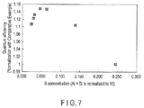
- s When s is 0, a good quantum efficiency cannot be obtained. On the other hand, when s is 0.245 or more, the quantum efficiency is reduced. In order to obtain a better quantum efficiency, s is 0.02 or more and 0.14 or less.
- the phosphor according to the present embodiment has all of the conditions described above, and thus it can emit yellow light with high efficiency when it is excited with light having emission peaks within a wavelength range of 250 to 500 nm.
- the yellow-emitting phosphor of the present embodiment is a material based on the Sr 2 Al 3 Si 7 ON 13 group crystals, in which Sr, Si, Al, O or N, which are elements forming the crystals, is substituted by another element, or another metal element such as Ce is solidified.
- the crystal structure is slightly changed by such a substitution, a large change of the positions of the atoms, such as breakage of a chemical bond between backbone atoms, rarely occurs.
- the position of the atom is provided by the crystal structure, the site occupied by the atom, and the coordinate thereof.
- the effects of the present embodiment can be exhibited within a range in which the basic crystal structure of the yellow-emitting phosphor of the present embodiment is not changed.
- the phosphor according to the present embodiment may sometimes be different in a lattice constant and lengths of chemical bonds M-N and M-O (distances between near neighbor atoms) from a case of Sr 2 Al 3 Si 7 ON 13 .
- the variation is within ⁇ 15% of the lattice constant of Sr 2 Al 3 Si 7 ON 13 and is within ⁇ 15% of the chemical bond lengths (Sr-N and Sr-O) in Sr 2 Al 3 Si 7 ON 13 , then the crystal structure is defined as unchanged.
- the lattice constant can be obtained by an X-ray diffraction or a neutron beam diffraction, and the lengths of the chemical bonds M-N and M-O (distances between near neighbor atoms) can be calculated from an atomic coordinate.
- the crystals belong to a space group Pna 21 (the 33rd in a space group shown in a literature ( International Tables for Crystallography, Volume A: Space-group symmetry, edited by T. Hahn, published by Springer (Netherlands) (publication date: 1983, the first editi on))).
- the lengths of the chemical bonds in Sr 2 Al 3 Si 7 ON 13 (Sr-N and Sr-O) can be calculated from the atomic coordinates shown in Table 1.
- the yellow-emitting phosphor of the present embodiment has the crystal structure described above.
- the chemical bond is broken and forms another crystal, and thus the effects by the present invention cannot be obtained.
- the yellow-emitting phosphor of the present embodiment is a material based on an inorganic compound having substantially the same crystal structure as that of Sr 2 Al 3 Si 7 ON 13 in which a part of the forming atoms M are substituted by the luminescent center Ce, and the element composition is defined in a predetermined range. In this case, the preferable property of the high quantum efficiency is shown.
- FIG. 1A is a projection view in the c-axis direction
- FIG. 1B is a projection view in the b-axis direction
- FIG. 1C is a projection view in the a-axis direction.
- 301 shows an atom Sr, and the atom is surrounded by an atom Si or Al 302, and an atom O or N 303.
- the crystals of Sr 2 Al 3 Si 7 ON 13 can be identified by an XRD or neutron diffraction.
- the yellow-emitting phosphor according to the present embodiment can be produced by mixing raw material powders including each element, and firing the mixture.
- a raw material for M can be selected from nitrides and carbides of M.
- a raw material for Al can be selected from nitrides, oxides and carbides of Al, and a raw material for Si (Si source) can be selected from nitrides, oxides and carbides of Si.
- a raw material for the luminescent center element Ce can be selected from chlorides, oxides and nitrides of Ce.
- a raw material for B (B source) can be selected from hydroxides of B, oxides of B, and the like.
- Nitrogen can be provided from a nitride raw material or by firing in an atmosphere including nitrogen, and oxygen can be provided from an oxide raw material or an oxide coating film on a surface of a nitride raw material.
- Sr 3 N 2 , CeCl 3 , Si 3 N 4 , AIN and B(OH) 3 which are source powders
- Sr 2 N or SrN, or a mixture thereof may be used instead of Sr 3 N 2 .
- the sources may be mixed, for example, using a mortar in a glove box. The mixed powder is put in a crucible and it is fired in predetermined conditions, whereby the phosphor according to the present embodiment can be obtained.
- the material for the crucible is not particularly limited, and can be selected from boron nitride, silicon nitride, silicon carbide, carbon, aluminum nitride, sialon, aluminum oxide, molybdenum, tungsten, and the like.
- the mixed powder in a pressure of atmospheric pressure or higher.
- the pressure is more preferably 5 atmospheres or higher, and the firing temperature is preferably within a range of 1500 to 2000°C.
- the firing temperature is more preferably from 1800 to 2000°C.
- Hydrogen may be contained in a content of up to about 50% in the atmosphere.
- the phosphor of the present embodiment is obtained by the firing at the temperature described above for 1 to 20 hours.
- the fired product may be taken out from the crucible and is cracked, and the firing may be performed again in the same conditions as above.
- a series of steps of taken out, cracking and firing are repeated 0 to about 10 times, the advantages of crystal particles being slightly fused to each other and a powder having uniform composition and crystal structure being easily produced can be obtained.
- the resulting product may be subjected to a post-treatment such as washing if necessary, thereby obtaining the phosphor according to one embodiment.
- a post-treatment such as washing if necessary, thereby obtaining the phosphor according to one embodiment.
- the washing for example, pure water, an acid, or the like may be used.
- an inorganic acid such as sulfuric acid, nitric acid, hydrochloric acid or hydrofluoric acid, an organic acid such as formic acid, acetic acid or oxalic acid, or a mixed acid thereof may be used.
- the resulting product Before or after the washing with an acid, the resulting product may be subjected to a post-annealing treatment, if necessary.
- the post-annealing treatment may be performed, for example, in a reduction atmosphere including nitrogen and hydrogen. When such a post-annealing treatment is performed, the crystallizability and the luminous efficiency are improved.
- a light-emitting device has a luminous layer including the phosphor described above, and a light source (light-emitting element) exciting the phosphor described above.
- FIG. 2 is a schematic view showing a structure of a light-emitting device according to one embodiment.
- leads 101 and 102 and a package cup 103 are disposed on a substrate 100.
- the substrate 100 and the package cup 103 are made of a resin.
- the package cup 103 has a recess 105 whose upper part is larger than its bottom part, and a side surface of this depression part acts as a reflection surface 104.
- a light-emitting element 106 is mounted at a center part of an almost circular bottom face of the recess 105 with an Ag paste, or the like.
- the light-emitting element 106 which can be used is an element capable of emitting light having an emission peak within a wavelength range of 400 to 500 nm.
- Such a light-emitting element may include, for example, a light-emitting diode, a laser diode, and the like. Specifically, it is exemplified by semiconductor GaN-type light-emitting elements, and the like, but it is not particularly limited.
- a p-electrode and an n-electrode (not shown in the figure) of the light-emitting element 106 are respectively connected to the lead 101 and the lead 102 with a bonding wires 107 and 108 made of Au or the like.
- the arrangement of the leads 101 and 102 may be appropriately changed.
- a flip-chip light-emitting element having the n-electrode and the p-electrode on the same surface may be used.
- problems resulting from wires such as breaking or separation of wires, and light absorption by wires can be solved, and a semiconductor light-emitting device having high reliability and high brightness can be obtained.
- a light-emitting element having an n-type substrate the following structure may be formed. An n-electrode is formed on a bottom surface of the n-type substrate of the light-emitting element, and a p-electrode is formed on a top surface of a p-type semiconductor layer laminated on the substrate. The n-electrode is mounted on a lead, and the p-electrode is connected to the other lead with a wire.
- a luminous layer 109 including a phosphor 110 is disposed in the recess 105 of the package cup 103.
- the luminous layer 109 for example, 5 to 60% by mass of the phosphor 110 is included in a resin layer 111 of a silicone resin.
- the phosphor according to the present embodiment includes Sr 2 Al 3 Si 7 ON 13 as the matrix, and such an oxynitride has a high covalency. For this reason, the phosphor according to the present embodiment is hydrophobic, and has a very good compatibility with a resin. Thus, scattering can be remarkably suppressed at an interface between the resin layer and the phosphor, and light extraction efficiency is improved.
- the yellow-emitting phosphor according to the present embodiment can emit yellow light with high efficiency.
- a white light-emitting device having a good luminescence property can be obtained by combination with a light-emitting element capable of emitting light having an emission peak within a wavelength range of 400 to 500 nm.
- a size and a kind of the light-emitting element 106, and dimensions and a shape of the recess 105 can be appropriately changed.
- the light-emitting device is not limited to the package cup-type device as shown in FIG. 2 , and can be appropriately changed. Specifically, when the phosphor of the embodiment is applied to a shell-type LED or a surface-mounting LED, the same effects as above can be obtained.
- FIG. 3 is a schematic view showing a structure of a light-emitting device according to another embodiment.
- a p-electrode and an n-electrode are formed on given areas of a heat-dissipating insulation substrate 201, and a light-emitting element 202 is disposed thereon.
- AIN As the material of the heat-dissipating insulation substrate 201, for example, AIN may be used.
- One electrode in the light-emitting element 202 is formed on the bottom face thereof, and is electrically connected to an n-electrode of the heat-dissipating insulation substrate 201.
- the other electrode in the light-emitting element 202 is connected to a p-electrode (not shown in the figure) on the heat-dissipating insulation substrate 201 through a gold wire 203.
- a light-emitting diode capable of emitting light having an emission peak within a wavelength range of 400 to 500 nm is used.
- a dome-shaped inside transparent resin layer 204, a luminous layer 205, and an outside transparent resin layer 206 are sequentially formed on the light-emitting element 202.
- the inside transparent resin layer 204 and the outside transparent resin layer 206 may be formed, for example, using silicone, or the like.
- the yellow-emitting phosphor 207 of the present embodiment is contained in a resin layer 208 formed of, for example, a silicone resin.
- the luminous layer 205 including the yellow-emitting phosphor according to the present embodiment can be conveniently produced employing a vacuum printing method or a drop coating method using a dispenser. Moreover, because the luminous layer 205 is put between the inside transparent resin layer 204 and the outside transparent resin layer 206, the effect to improve the extraction efficiency can be obtained.
- the luminous layer in the light-emitting device may include a phosphor capable of emitting green light by excitation with blue light and a phosphor capable of emitting red light by excitation with blue light, together with the yellow-emitting phosphor of the present embodiment.
- a white light-emitting device having more excellent color rendering property can be obtained.
- a phosphor having a different luminescent color is included in a separate luminous layer, whereby a laminated structure can be produced in which a luminous layer including a yellow-emitting phosphor, a luminous layer including a green-emitting phosphor, and a luminous layer including a red-emitting phosphor are included.
- Yellow emission can also be obtained when the yellow-emitting phosphor according to the present embodiment is excited with light with the ultraviolet region having a peak within a wavelength range of 250 to 430 nm.
- a white light-emitting device therefore, can also be formed by combining the phosphor according to the present embodiment with, for example, a phosphor capable of emitting blue light (a peak wavelength: 400 to 490 nm) by excitation with ultraviolet light and a light-emitting element such as an ultraviolet light-emitting diode.
- the luminous layer in the white light-emitting device may include a phosphor capable of emitting light having a peak within another wavelength range by excitation with ultraviolet light together with the yellow-emitting phosphor of the present embodiment.
- Such a phosphor may include, for example, a phosphor capable of emitting red light by excitation with ultraviolet light, a phosphor capable of emitting green light by excitation with ultraviolet light, and the like.
- the phosphor of the present embodiment can emit yellow light with high efficiency.
- a yellow-emitting phosphor of the present embodiment is combined with a light-emitting element capable of emitting light having an emission peak within a wavelength range of 250 to 500 nm, the white light-emitting device having an excellent luminescence property can be obtained using fewer kinds of the phosphors.
- Sr 3 N 2 , CeCl 3 , Si 3 N 4 , AlN, and B(OH) 3 were prepared as a Sr source, a Ce source, a Si source, a Al source, and a 8 source, and each source was weighed in a glove box. Blending masses of Sr 3 N 2 , CeCl 3 , Si 3 N 4 , AlN and B(OH) 3 were 2.902 g, 0.148 g, 5.262 g, 1.537 g and 0.004 g, respectively. The mixture powders were dry-mixed in an agate mortar.
- the obtained mixture was put into a boron nitride crucible, and the mixture was fired at 1750°C for 15 hours in a nitrogen atmosphere having a pressure of 7.5 atmospheres, thereby obtaining a phosphor of Example 1.
- the obtained phosphor was powder having a body color of yellow, and it was confirmed that the material emitted yellow light when it was excited with black light.
- Emission spectra obtained by exciting this phosphor with a xenon lamp in which the light was spectrally dispersed into an emission wavelength of 450 nm are shown in FIG. 4 .
- an emission having a narrow half-width at near 450 nm is reflection of excitation light, and is not emission of the phosphor.
- a high emission intensity was observed at a peak wavelength of 551 nm.
- a light-emitting device having a structure shown in FIG. 3 was produced using the phosphor of the present Example.
- a fight-emitting diode having an emission peak wavelength of 460 nm was joined to the substrate through a solder as a light-emitting element 202.
- One electrode of a light-emitting element 202 was formed on the bottom face thereof, and was electrically connected to the n-electrode of the AlN substrate 201.
- the other electrode of the light-emitting element 202 was connected to the p-electrode (not shown in the figure) on the AIN substrate 401 through a gold wire 403.
- An inside transparent resin layer 204, a luminous layer 205, and an outside transparent resin layer 206 were sequentially formed in a dome-shape on the light-emitting element 202, thereby producing a light-emitting device of the present Example.
- a silicone resin was used as a material of the inside transparent resin layer 204, and the layer was formed using a dispenser.
- a transparent resin including 25% by mass of the phosphor of the present Example was used.
- the transparent resin used was a silicone resin.
- the same silicone resin as used in the formation of the inside transparent resin layer 204 was used.
- This light-emitting device was installed in an integrating sphere.
- the color temperature and Ra were obtained from an instantaneous multichannel spectrometer.
- a white light-emitting device of the present embodiment could be obtained by combining the phosphor of the present Example with a blue LED having an emission peak wavelength of 460 nm.
- a high power white LED having a high luminous efficiency can be obtained from such a white light-emitting device.
- Example 2 Mass (g) Heating Temperature (°C) Sr 3 N 2 CeCl 2 Si 3 N 4 AlN B(OH) 3
- Example 1 2.902 0.148 5.262 1.537 0.004 1750
- Example 2 2.902 0.148 5.262 1.537 0.003 1700
- Example 3 2.887 0.185 5.402 1.414 0.003 1700
- Example 4 3.055 0.222 5.402 1.414 0.002 1800
- Example 5 2.887 0.185 5.402 1.414 0.006 1800
- Example 6 2.872 0.222 5.262 1.537 0.013 1800 Comparative Example 1 2.887 0.185 5.402 1.414 0.023 1800
- the phosphors of Examples 2 to 6 and Comparative Example were all powders having a body color of yellow, and it was confirmed that the materials emitted yellow light when they were excited with black light.
- an XRD pattern of the phosphor from Example 4 is shown in FIG. 5 and a JCPDS card (No. 01-077-9609) is shown in FIG. 6 . It can be seen that a desired phosphor is roughly formed in a single phase from the comparison of FIG. 5 with FIG. 6 .
- XRD patterns of the phosphors of Examples 1 to 3, 5 and 6 were the same as that of the phosphor of Example 4.
- Example 1 Example 2
- Example 4 2 ⁇ [°] 8.6 8.58 8.6 11.18 11.17 11.16 15.08 15.11 15.14 18.32 18.31 18.3 19.86 19.83 19.88 23.08 23.1 23.08 24.93 24.91 24.95 25.8 25.74 25.68 26.05 26.02 26.06 26.62 26.61 26.63 28.88 28.87 - 29.36 29.38 29.36 30.32 30.3 30.27 30.99 30.97 30.97 31.68 31.69 31.68 33.1 33.05 33.09 33.67 33.64 33.67 34.02 34.03 34.04 34.44 34.41 34.46 35.3 35.27 35.33 36.19 36.15 36.13 36.61 36.62 36.6 37.34 37.34 - Table 4
- Example 1 Example 2
- Example 4 28[°] - - 38.01 38.68 38.65 38.64 39.04 - - 39.51 39.49 - 40.54 40.55 - 41.
- Light-emitting devices were produced in the same manner as above except that the phosphors of Examples 2 to 6 were used, and the properties thereof were examined in the same manner as above. It was confirmed that these light-emitting devices had the same properties as those of the light-emitting device using the phosphor of Example 1.
- Table 5 summarizes the results of a chemical analysis of the phosphors of Examples 1 to 6 and Comparative Example using inductively coupled plasma (ICP).
- Table 6 summarizes values of x, y, z, u, s and the like in the following Formula 1.
- the value of s is 0.245, which is out of the range below. 0 ⁇ x ⁇ 1 , 0.8 ⁇ y ⁇ 1.1 , 2 ⁇ z ⁇ 3.5 , 1 ⁇ u ⁇ 1 5 ⁇ z - u , 13 ⁇ u + w ⁇ 15 , and 0 ⁇ s ⁇ 0.245.
- Quantum efficiencies of the phosphors of Examples 1 to 6 and Comparative Example were obtained according to a method described below. Specifically, a quantum efficiency was measured using (a fluorescence spectrophotometer (an absolute quantum yield measurement system C9920-02G) manufactured by Hamamatsu Photonics K.K.).
- FIG. 7 is a graph in which relationships between a B concentration and a quantum efficiency in each phosphor are plotted.
- the B concentration here is a value obtained by normalization, supposing that a total of an Al concentration and an Si concentration corresponds to the value of s in the Formula 1.
- the quantum efficiency is a value obtained by normalization using the value of Comparative Example. It can be seen that when the normalized B concentration is within a range of (0 ⁇ s ⁇ 0.245), the good quantum efficiency is obtained, and when s is 0.023 to 0.139, a quantum efficiency of 1.1 or more can be obtained compared to a value when the quantum efficiency of Comparative Example is normalized as 1. (M 1-x Ce x ) 2y Al z Si 10-z O u N w B S Formula 1
- the materials can emit yellow light with high efficiency. It was confirmed that even if a material includes the same elements, when the content of boron is out of the predetermined range, the high quantum efficiency cannot be obtained.
- the yellow-emitting phosphors having a high quantum efficiency and capable of obtaining a white LED illumination with high efficiency are provided.
- the yellow-emitting phosphor of the present embodiment is combined with a blue LED, the white light-emitting device having a high efficiency can be obtained.
Landscapes
- Chemical & Material Sciences (AREA)
- Engineering & Computer Science (AREA)
- Inorganic Chemistry (AREA)
- Materials Engineering (AREA)
- Organic Chemistry (AREA)
- Physics & Mathematics (AREA)
- Microelectronics & Electronic Packaging (AREA)
- Optics & Photonics (AREA)
- General Engineering & Computer Science (AREA)
- Luminescent Compositions (AREA)
- Led Device Packages (AREA)
Claims (14)
- Leuchtstoff, der einen Lumineszenzpeak innerhalb eines Wellenlängenbereichs von 500 bis 600 nm aufweist, wenn er mit Licht, das einen Emissionspeak innerhalb eines Wellenlängenbereichs von 250 bis 500 nm aufweist, angeregt wird, dadurch gekennzeichnet, dass er eine Zusammensetzung umfasst, die durch Formel 1 unten dargestellt wird:
(M1_xCex)2yAlzSi10-zOuNwBS Formel 1
worin M Sr darstellt und ein Teil des Sr durch zumindest eines, das aus der Gruppe ausgewählt ist, bestehend aus Ba, Ca und Mg, ersetzt sein kann; und x, y, z, u, w und s die folgenden Bedingungen erfüllen:

- Leuchtstoff gemäß Anspruch 1, dadurch gekennzeichnet, dass x 0,001 ≤ x ≤ 0,5 erfüllt.
- Leuchtstoff gemäß Anspruch 1, dadurch gekennzeichnet, dass y 0,85 ≤ y ≤ 1,06 erfüllt.
- Leuchtstoff gemäß Anspruch 1, dadurch gekennzeichnet, dass z 2,5 ≤ z ≤ 3,3 erfüllt.
- Leuchtstoff gemäß Anspruch 1, dadurch gekennzeichnet, dass u 0,001 ≤ u ≤ 0,8 erfüllt.
- Leuchtstoff gemäß Anspruch 1, dadurch gekennzeichnet, dass z - u 2 ≤ z - u erfüllt.
- Leuchtstoff gemäß Anspruch 1, dadurch gekennzeichnet, dass u + w 13,2 ≤ u + w ≤ 14,2 erfüllt.
- Leuchtstoff gemäß Anspruch 1, dadurch gekennzeichnet, dass der Leuchtstoff zumindest zehn Peaks bei Beugungswinkeln (2θ) von 15,05 bis 15,15°, 23,03 bis 23,13°, 24,87 bis 24,97°, 25,68 bis 25,8°, 25,97 bis 26,07°, 29,33 bis 29,43°, 30,92 bis 31,02°, 31,65 bis 31,75°, 31,88 bis 31,98°, 33,02 bis 33,12°, 33,59 bis 33,69°, 34,35 bis 34,46°, 35,2 bis 35,33°, 36,02 bis 36,12°, 36,55 bis 36,65°, 37,3 bis 37,4° und 56,5 bis 56,6° in einem Röntgenbeugungsverfahren nach Bragg-Brendano unter Verwendung der Cu-Kα-Linie aufweist.
- Lichtemittierende Vorrichtung, dadurch gekennzeichnet, dass sie umfasst:eine Lichtquelle, die Licht, das einen Emissionspeak in einem Wellenlängenbereich von 250 bis 500 nm aufweist, emittiert; undeine Leuchtschicht, die einen gelb emittierenden Leuchtstoff umfasst, der den Leuchtstoff gemäß einem beliebigen der Ansprüche 1 bis 8 umfasst.
- Lichtemittierende Vorrichtung gemäß Anspruch 9, dadurch gekennzeichnet, dass sie ferner ein Wärme-ableitendes Isolationssubstrat, auf dem die Lichtquelle angeordnet ist, umfasst.
- Lichtemittierende Vorrichtung gemäß Anspruch 9, dadurch gekennzeichnet, dass die Leuchtschicht ferner einen grün emittierenden Leuchtstoff und einen rot emittierenden Leuchtstoff umfasst.
- Lichtemittierende Vorrichtung gemäß Anspruch 11, dadurch gekennzeichnet, dass die Leuchtschicht eine laminierte Struktur aus drei Schichten aufweist und jeder des gelb emittierenden Leuchtstoffs, des grün emittierenden Leuchtstoffs und des rot emittierenden Leuchtstoffs in individuellen separaten Leuchtschichten enthalten ist.
- Lichtemittierende Vorrichtung gemäß Anspruch 9, dadurch gekennzeichnet, dass die Lichtquelle Licht, das eine Wellenlänge von 250 bis 430 nm aufweist, emittiert.
- Lichtemittierende Vorrichtung gemäß Anspruch 13, dadurch gekennzeichnet, dass die Leuchtschicht ferner einen Leuchtstoff umfasst, der einen Lumineszenzpeak innerhalb eines Wellenlängenbereichs von 400 bis 490 nm aufweist, wenn er durch das Licht von der Lichtquelle angeregt wird.
Applications Claiming Priority (1)
| Application Number | Priority Date | Filing Date | Title |
|---|---|---|---|
| JP2013103464A JP2014224184A (ja) | 2013-05-15 | 2013-05-15 | 蛍光体および発光装置 |
Publications (2)
| Publication Number | Publication Date |
|---|---|
| EP2803716A1 EP2803716A1 (de) | 2014-11-19 |
| EP2803716B1 true EP2803716B1 (de) | 2016-02-03 |
Family
ID=50101765
Family Applications (1)
| Application Number | Title | Priority Date | Filing Date |
|---|---|---|---|
| EP14155102.8A Not-in-force EP2803716B1 (de) | 2013-05-15 | 2014-02-13 | Sialon leuchtstoff |
Country Status (6)
| Country | Link |
|---|---|
| US (1) | US20140339978A1 (de) |
| EP (1) | EP2803716B1 (de) |
| JP (1) | JP2014224184A (de) |
| KR (1) | KR20140135092A (de) |
| CN (1) | CN104164235A (de) |
| TW (1) | TWI516570B (de) |
Families Citing this family (2)
| Publication number | Priority date | Publication date | Assignee | Title |
|---|---|---|---|---|
| JP2015211202A (ja) * | 2014-04-30 | 2015-11-24 | 株式会社東芝 | 発光装置 |
| CN106915955B (zh) * | 2017-01-24 | 2020-06-09 | 江苏师范大学 | 一种绿色荧光陶瓷材料、制备方法及其应用 |
Family Cites Families (7)
| Publication number | Priority date | Publication date | Assignee | Title |
|---|---|---|---|---|
| WO2006087661A1 (en) * | 2005-02-21 | 2006-08-24 | Philips Intellectual Property & Standards Gmbh | Illumination system comprising a radiation source and a luminescent material |
| KR101264580B1 (ko) * | 2005-09-27 | 2013-05-14 | 미쓰비시 가가꾸 가부시키가이샤 | 형광체 및 그 제조방법, 및 상기 형광체를 사용한 발광장치 |
| EP2518129B1 (de) * | 2006-03-10 | 2014-04-23 | Kabushiki Kaisha Toshiba | Lumineszierendes Material und lichtemittierende Vorrichtung |
| US8469760B2 (en) * | 2006-03-31 | 2013-06-25 | Dowa Electronics Materials Co., Ltd. | Light emitting device and method for producing same |
| US8513876B2 (en) * | 2007-05-22 | 2013-08-20 | National Institute For Materials Science | Fluorescent substance, method for producing the same, and light-emitting device using the same |
| WO2010098141A1 (ja) * | 2009-02-26 | 2010-09-02 | 日亜化学工業株式会社 | 蛍光体及びその製造方法並びにこれを用いた発光装置 |
| JP5634352B2 (ja) * | 2011-08-24 | 2014-12-03 | 株式会社東芝 | 蛍光体、発光装置および蛍光体の製造方法 |
-
2013
- 2013-05-15 JP JP2013103464A patent/JP2014224184A/ja active Pending
-
2014
- 2014-02-13 EP EP14155102.8A patent/EP2803716B1/de not_active Not-in-force
- 2014-02-18 TW TW103105194A patent/TWI516570B/zh not_active IP Right Cessation
- 2014-02-20 US US14/184,890 patent/US20140339978A1/en not_active Abandoned
- 2014-02-21 CN CN201410060927.4A patent/CN104164235A/zh active Pending
- 2014-02-24 KR KR20140021121A patent/KR20140135092A/ko not_active Abandoned
Also Published As
| Publication number | Publication date |
|---|---|
| US20140339978A1 (en) | 2014-11-20 |
| TWI516570B (zh) | 2016-01-11 |
| JP2014224184A (ja) | 2014-12-04 |
| EP2803716A1 (de) | 2014-11-19 |
| CN104164235A (zh) | 2014-11-26 |
| TW201446937A (zh) | 2014-12-16 |
| KR20140135092A (ko) | 2014-11-25 |
Similar Documents
| Publication | Publication Date | Title |
|---|---|---|
| JP5762929B2 (ja) | 蛍光体、発光装置、および蛍光体の製造方法 | |
| EP2597131B1 (de) | Leuchtstoffmaterial auf der Basis von (Sr1-xEux)aSibAlOcNd | |
| EP2998382A1 (de) | Phosphor, verfahren zur herstellung davon und lichtemittierende vorrichtung damit | |
| EP2915862A1 (de) | Leuchtstoff und Herstellungsverfahren von Phosphor und lichtemittierende Vorrichtung damit | |
| EP2778211A1 (de) | Phosphor und lichtemittierende Vorrichtung damit | |
| EP2910621A1 (de) | Phosphor, lichtemittierende vorrichtung und verfahren zur herstellung von phosphor | |
| US8957447B2 (en) | Phosphor | |
| EP2803716B1 (de) | Sialon leuchtstoff | |
| EP2781576A1 (de) | Leuchtstoff, lichtemittierende Vorrichtung und Verfahren zur Herstellung des Phosphors | |
| EP2918654A2 (de) | Phosphor, verfahren zur herstellung davon und lichtemittierende vorrichtung damit | |
| EP2999015A1 (de) | Phosphor, lichtemittierende vorrichtung und verfahren zur herstellung von phosphor | |
| JP2016056241A (ja) | 蛍光体、その製造方法、およびその蛍光体を用いた発光装置 | |
| US20160083648A1 (en) | Phosphor, method for producing the same, and light-emitting device using the same | |
| JP2014127500A (ja) | 白色発光装置 |
Legal Events
| Date | Code | Title | Description |
|---|---|---|---|
| PUAI | Public reference made under article 153(3) epc to a published international application that has entered the european phase |
Free format text: ORIGINAL CODE: 0009012 |
|
| 17P | Request for examination filed |
Effective date: 20140213 |
|
| AK | Designated contracting states |
Kind code of ref document: A1 Designated state(s): AL AT BE BG CH CY CZ DE DK EE ES FI FR GB GR HR HU IE IS IT LI LT LU LV MC MK MT NL NO PL PT RO RS SE SI SK SM TR |
|
| AX | Request for extension of the european patent |
Extension state: BA ME |
|
| REG | Reference to a national code |
Ref country code: DE Ref legal event code: R079 Ref document number: 602014000812 Country of ref document: DE Free format text: PREVIOUS MAIN CLASS: C09K0011640000 Ipc: H01L0033500000 |
|
| GRAP | Despatch of communication of intention to grant a patent |
Free format text: ORIGINAL CODE: EPIDOSNIGR1 |
|
| RIC1 | Information provided on ipc code assigned before grant |
Ipc: C09K 11/64 20060101ALI20150603BHEP Ipc: H01L 33/50 20100101AFI20150603BHEP |
|
| INTG | Intention to grant announced |
Effective date: 20150622 |
|
| GRAS | Grant fee paid |
Free format text: ORIGINAL CODE: EPIDOSNIGR3 |
|
| RIN1 | Information on inventor provided before grant (corrected) |
Inventor name: HATTORI, YASUSHI Inventor name: FUKUDA, YUMI Inventor name: OKADA, AOI Inventor name: ALBESSARD, KEIKO Inventor name: KATO, MASAHIRO Inventor name: MITSUISHI, IWAO |
|
| GRAA | (expected) grant |
Free format text: ORIGINAL CODE: 0009210 |
|
| AK | Designated contracting states |
Kind code of ref document: B1 Designated state(s): AL AT BE BG CH CY CZ DE DK EE ES FI FR GB GR HR HU IE IS IT LI LT LU LV MC MK MT NL NO PL PT RO RS SE SI SK SM TR |
|
| REG | Reference to a national code |
Ref country code: GB Ref legal event code: FG4D |
|
| REG | Reference to a national code |
Ref country code: FR Ref legal event code: PLFP Year of fee payment: 3 |
|
| REG | Reference to a national code |
Ref country code: AT Ref legal event code: REF Ref document number: 774056 Country of ref document: AT Kind code of ref document: T Effective date: 20160215 Ref country code: CH Ref legal event code: EP |
|
| REG | Reference to a national code |
Ref country code: IE Ref legal event code: FG4D |
|
| REG | Reference to a national code |
Ref country code: DE Ref legal event code: R096 Ref document number: 602014000812 Country of ref document: DE |
|
| PGFP | Annual fee paid to national office [announced via postgrant information from national office to epo] |
Ref country code: DE Payment date: 20160209 Year of fee payment: 3 |
|
| PGFP | Annual fee paid to national office [announced via postgrant information from national office to epo] |
Ref country code: FR Payment date: 20160208 Year of fee payment: 3 |
|
| REG | Reference to a national code |
Ref country code: LT Ref legal event code: MG4D Ref country code: NL Ref legal event code: MP Effective date: 20160203 |
|
| REG | Reference to a national code |
Ref country code: AT Ref legal event code: MK05 Ref document number: 774056 Country of ref document: AT Kind code of ref document: T Effective date: 20160203 |
|
| PG25 | Lapsed in a contracting state [announced via postgrant information from national office to epo] |
Ref country code: IT Free format text: LAPSE BECAUSE OF FAILURE TO SUBMIT A TRANSLATION OF THE DESCRIPTION OR TO PAY THE FEE WITHIN THE PRESCRIBED TIME-LIMIT Effective date: 20160203 Ref country code: GR Free format text: LAPSE BECAUSE OF FAILURE TO SUBMIT A TRANSLATION OF THE DESCRIPTION OR TO PAY THE FEE WITHIN THE PRESCRIBED TIME-LIMIT Effective date: 20160504 Ref country code: NO Free format text: LAPSE BECAUSE OF FAILURE TO SUBMIT A TRANSLATION OF THE DESCRIPTION OR TO PAY THE FEE WITHIN THE PRESCRIBED TIME-LIMIT Effective date: 20160503 Ref country code: HR Free format text: LAPSE BECAUSE OF FAILURE TO SUBMIT A TRANSLATION OF THE DESCRIPTION OR TO PAY THE FEE WITHIN THE PRESCRIBED TIME-LIMIT Effective date: 20160203 Ref country code: FI Free format text: LAPSE BECAUSE OF FAILURE TO SUBMIT A TRANSLATION OF THE DESCRIPTION OR TO PAY THE FEE WITHIN THE PRESCRIBED TIME-LIMIT Effective date: 20160203 |
|
| PG25 | Lapsed in a contracting state [announced via postgrant information from national office to epo] |
Ref country code: RS Free format text: LAPSE BECAUSE OF FAILURE TO SUBMIT A TRANSLATION OF THE DESCRIPTION OR TO PAY THE FEE WITHIN THE PRESCRIBED TIME-LIMIT Effective date: 20160203 Ref country code: AT Free format text: LAPSE BECAUSE OF FAILURE TO SUBMIT A TRANSLATION OF THE DESCRIPTION OR TO PAY THE FEE WITHIN THE PRESCRIBED TIME-LIMIT Effective date: 20160203 Ref country code: PT Free format text: LAPSE BECAUSE OF FAILURE TO SUBMIT A TRANSLATION OF THE DESCRIPTION OR TO PAY THE FEE WITHIN THE PRESCRIBED TIME-LIMIT Effective date: 20160603 Ref country code: LV Free format text: LAPSE BECAUSE OF FAILURE TO SUBMIT A TRANSLATION OF THE DESCRIPTION OR TO PAY THE FEE WITHIN THE PRESCRIBED TIME-LIMIT Effective date: 20160203 Ref country code: IS Free format text: LAPSE BECAUSE OF FAILURE TO SUBMIT A TRANSLATION OF THE DESCRIPTION OR TO PAY THE FEE WITHIN THE PRESCRIBED TIME-LIMIT Effective date: 20160603 Ref country code: BE Free format text: LAPSE BECAUSE OF NON-PAYMENT OF DUE FEES Effective date: 20160229 Ref country code: LT Free format text: LAPSE BECAUSE OF FAILURE TO SUBMIT A TRANSLATION OF THE DESCRIPTION OR TO PAY THE FEE WITHIN THE PRESCRIBED TIME-LIMIT Effective date: 20160203 Ref country code: SE Free format text: LAPSE BECAUSE OF FAILURE TO SUBMIT A TRANSLATION OF THE DESCRIPTION OR TO PAY THE FEE WITHIN THE PRESCRIBED TIME-LIMIT Effective date: 20160203 Ref country code: PL Free format text: LAPSE BECAUSE OF FAILURE TO SUBMIT A TRANSLATION OF THE DESCRIPTION OR TO PAY THE FEE WITHIN THE PRESCRIBED TIME-LIMIT Effective date: 20160203 Ref country code: NL Free format text: LAPSE BECAUSE OF FAILURE TO SUBMIT A TRANSLATION OF THE DESCRIPTION OR TO PAY THE FEE WITHIN THE PRESCRIBED TIME-LIMIT Effective date: 20160203 |
|
| PG25 | Lapsed in a contracting state [announced via postgrant information from national office to epo] |
Ref country code: EE Free format text: LAPSE BECAUSE OF FAILURE TO SUBMIT A TRANSLATION OF THE DESCRIPTION OR TO PAY THE FEE WITHIN THE PRESCRIBED TIME-LIMIT Effective date: 20160203 Ref country code: DK Free format text: LAPSE BECAUSE OF FAILURE TO SUBMIT A TRANSLATION OF THE DESCRIPTION OR TO PAY THE FEE WITHIN THE PRESCRIBED TIME-LIMIT Effective date: 20160203 |
|
| REG | Reference to a national code |
Ref country code: DE Ref legal event code: R097 Ref document number: 602014000812 Country of ref document: DE |
|
| PG25 | Lapsed in a contracting state [announced via postgrant information from national office to epo] |
Ref country code: CZ Free format text: LAPSE BECAUSE OF FAILURE TO SUBMIT A TRANSLATION OF THE DESCRIPTION OR TO PAY THE FEE WITHIN THE PRESCRIBED TIME-LIMIT Effective date: 20160203 Ref country code: SK Free format text: LAPSE BECAUSE OF FAILURE TO SUBMIT A TRANSLATION OF THE DESCRIPTION OR TO PAY THE FEE WITHIN THE PRESCRIBED TIME-LIMIT Effective date: 20160203 Ref country code: SM Free format text: LAPSE BECAUSE OF FAILURE TO SUBMIT A TRANSLATION OF THE DESCRIPTION OR TO PAY THE FEE WITHIN THE PRESCRIBED TIME-LIMIT Effective date: 20160203 Ref country code: RO Free format text: LAPSE BECAUSE OF FAILURE TO SUBMIT A TRANSLATION OF THE DESCRIPTION OR TO PAY THE FEE WITHIN THE PRESCRIBED TIME-LIMIT Effective date: 20160203 |
|
| REG | Reference to a national code |
Ref country code: IE Ref legal event code: MM4A |
|
| PLBE | No opposition filed within time limit |
Free format text: ORIGINAL CODE: 0009261 |
|
| STAA | Information on the status of an ep patent application or granted ep patent |
Free format text: STATUS: NO OPPOSITION FILED WITHIN TIME LIMIT |
|
| PG25 | Lapsed in a contracting state [announced via postgrant information from national office to epo] |
Ref country code: BE Free format text: LAPSE BECAUSE OF FAILURE TO SUBMIT A TRANSLATION OF THE DESCRIPTION OR TO PAY THE FEE WITHIN THE PRESCRIBED TIME-LIMIT Effective date: 20160203 |
|
| 26N | No opposition filed |
Effective date: 20161104 |
|
| PG25 | Lapsed in a contracting state [announced via postgrant information from national office to epo] |
Ref country code: IE Free format text: LAPSE BECAUSE OF NON-PAYMENT OF DUE FEES Effective date: 20160213 |
|
| PG25 | Lapsed in a contracting state [announced via postgrant information from national office to epo] |
Ref country code: SI Free format text: LAPSE BECAUSE OF FAILURE TO SUBMIT A TRANSLATION OF THE DESCRIPTION OR TO PAY THE FEE WITHIN THE PRESCRIBED TIME-LIMIT Effective date: 20160203 Ref country code: BG Free format text: LAPSE BECAUSE OF FAILURE TO SUBMIT A TRANSLATION OF THE DESCRIPTION OR TO PAY THE FEE WITHIN THE PRESCRIBED TIME-LIMIT Effective date: 20160503 |
|
| PG25 | Lapsed in a contracting state [announced via postgrant information from national office to epo] |
Ref country code: MT Free format text: LAPSE BECAUSE OF FAILURE TO SUBMIT A TRANSLATION OF THE DESCRIPTION OR TO PAY THE FEE WITHIN THE PRESCRIBED TIME-LIMIT Effective date: 20160203 |
|
| REG | Reference to a national code |
Ref country code: DE Ref legal event code: R119 Ref document number: 602014000812 Country of ref document: DE |
|
| REG | Reference to a national code |
Ref country code: CH Ref legal event code: PL |
|
| PG25 | Lapsed in a contracting state [announced via postgrant information from national office to epo] |
Ref country code: LI Free format text: LAPSE BECAUSE OF NON-PAYMENT OF DUE FEES Effective date: 20170228 Ref country code: CH Free format text: LAPSE BECAUSE OF NON-PAYMENT OF DUE FEES Effective date: 20170228 |
|
| REG | Reference to a national code |
Ref country code: FR Ref legal event code: ST Effective date: 20171031 |
|
| PG25 | Lapsed in a contracting state [announced via postgrant information from national office to epo] |
Ref country code: DE Free format text: LAPSE BECAUSE OF NON-PAYMENT OF DUE FEES Effective date: 20170901 Ref country code: FR Free format text: LAPSE BECAUSE OF NON-PAYMENT OF DUE FEES Effective date: 20170228 |
|
| PG25 | Lapsed in a contracting state [announced via postgrant information from national office to epo] |
Ref country code: ES Free format text: LAPSE BECAUSE OF FAILURE TO SUBMIT A TRANSLATION OF THE DESCRIPTION OR TO PAY THE FEE WITHIN THE PRESCRIBED TIME-LIMIT Effective date: 20160203 Ref country code: HU Free format text: LAPSE BECAUSE OF FAILURE TO SUBMIT A TRANSLATION OF THE DESCRIPTION OR TO PAY THE FEE WITHIN THE PRESCRIBED TIME-LIMIT; INVALID AB INITIO Effective date: 20140213 |
|
| PG25 | Lapsed in a contracting state [announced via postgrant information from national office to epo] |
Ref country code: MK Free format text: LAPSE BECAUSE OF FAILURE TO SUBMIT A TRANSLATION OF THE DESCRIPTION OR TO PAY THE FEE WITHIN THE PRESCRIBED TIME-LIMIT Effective date: 20160203 Ref country code: MC Free format text: LAPSE BECAUSE OF FAILURE TO SUBMIT A TRANSLATION OF THE DESCRIPTION OR TO PAY THE FEE WITHIN THE PRESCRIBED TIME-LIMIT Effective date: 20160203 Ref country code: LU Free format text: LAPSE BECAUSE OF NON-PAYMENT OF DUE FEES Effective date: 20160213 Ref country code: CY Free format text: LAPSE BECAUSE OF FAILURE TO SUBMIT A TRANSLATION OF THE DESCRIPTION OR TO PAY THE FEE WITHIN THE PRESCRIBED TIME-LIMIT Effective date: 20160203 Ref country code: MT Free format text: LAPSE BECAUSE OF FAILURE TO SUBMIT A TRANSLATION OF THE DESCRIPTION OR TO PAY THE FEE WITHIN THE PRESCRIBED TIME-LIMIT Effective date: 20160229 |
|
| GBPC | Gb: european patent ceased through non-payment of renewal fee |
Effective date: 20180213 |
|
| PG25 | Lapsed in a contracting state [announced via postgrant information from national office to epo] |
Ref country code: AL Free format text: LAPSE BECAUSE OF FAILURE TO SUBMIT A TRANSLATION OF THE DESCRIPTION OR TO PAY THE FEE WITHIN THE PRESCRIBED TIME-LIMIT Effective date: 20160203 Ref country code: TR Free format text: LAPSE BECAUSE OF FAILURE TO SUBMIT A TRANSLATION OF THE DESCRIPTION OR TO PAY THE FEE WITHIN THE PRESCRIBED TIME-LIMIT Effective date: 20160203 |
|
| PG25 | Lapsed in a contracting state [announced via postgrant information from national office to epo] |
Ref country code: GB Free format text: LAPSE BECAUSE OF NON-PAYMENT OF DUE FEES Effective date: 20180213 |