EP2802851B1 - Six-axis force-torque sensor - Google Patents
Six-axis force-torque sensor Download PDFInfo
- Publication number
- EP2802851B1 EP2802851B1 EP13704501.9A EP13704501A EP2802851B1 EP 2802851 B1 EP2802851 B1 EP 2802851B1 EP 13704501 A EP13704501 A EP 13704501A EP 2802851 B1 EP2802851 B1 EP 2802851B1
- Authority
- EP
- European Patent Office
- Prior art keywords
- sensing device
- electrode
- electrode structure
- bottom electrode
- electrodes
- Prior art date
- Legal status (The legal status is an assumption and is not a legal conclusion. Google has not performed a legal analysis and makes no representation as to the accuracy of the status listed.)
- Active
Links
Images




Classifications
-
- G—PHYSICS
- G01—MEASURING; TESTING
- G01L—MEASURING FORCE, STRESS, TORQUE, WORK, MECHANICAL POWER, MECHANICAL EFFICIENCY, OR FLUID PRESSURE
- G01L1/00—Measuring force or stress, in general
- G01L1/14—Measuring force or stress, in general by measuring variations in capacitance or inductance of electrical elements, e.g. by measuring variations of frequency of electrical oscillators
- G01L1/142—Measuring force or stress, in general by measuring variations in capacitance or inductance of electrical elements, e.g. by measuring variations of frequency of electrical oscillators using capacitors
- G01L1/148—Measuring force or stress, in general by measuring variations in capacitance or inductance of electrical elements, e.g. by measuring variations of frequency of electrical oscillators using capacitors using semiconductive material, e.g. silicon
-
- G—PHYSICS
- G01—MEASURING; TESTING
- G01L—MEASURING FORCE, STRESS, TORQUE, WORK, MECHANICAL POWER, MECHANICAL EFFICIENCY, OR FLUID PRESSURE
- G01L1/00—Measuring force or stress, in general
- G01L1/14—Measuring force or stress, in general by measuring variations in capacitance or inductance of electrical elements, e.g. by measuring variations of frequency of electrical oscillators
- G01L1/142—Measuring force or stress, in general by measuring variations in capacitance or inductance of electrical elements, e.g. by measuring variations of frequency of electrical oscillators using capacitors
-
- G—PHYSICS
- G01—MEASURING; TESTING
- G01L—MEASURING FORCE, STRESS, TORQUE, WORK, MECHANICAL POWER, MECHANICAL EFFICIENCY, OR FLUID PRESSURE
- G01L1/00—Measuring force or stress, in general
- G01L1/14—Measuring force or stress, in general by measuring variations in capacitance or inductance of electrical elements, e.g. by measuring variations of frequency of electrical oscillators
- G01L1/142—Measuring force or stress, in general by measuring variations in capacitance or inductance of electrical elements, e.g. by measuring variations of frequency of electrical oscillators using capacitors
- G01L1/144—Measuring force or stress, in general by measuring variations in capacitance or inductance of electrical elements, e.g. by measuring variations of frequency of electrical oscillators using capacitors with associated circuitry
-
- G—PHYSICS
- G01—MEASURING; TESTING
- G01L—MEASURING FORCE, STRESS, TORQUE, WORK, MECHANICAL POWER, MECHANICAL EFFICIENCY, OR FLUID PRESSURE
- G01L3/00—Measuring torque, work, mechanical power, or mechanical efficiency, in general
- G01L3/02—Rotary-transmission dynamometers
-
- G—PHYSICS
- G01—MEASURING; TESTING
- G01L—MEASURING FORCE, STRESS, TORQUE, WORK, MECHANICAL POWER, MECHANICAL EFFICIENCY, OR FLUID PRESSURE
- G01L5/00—Apparatus for, or methods of, measuring force, work, mechanical power, or torque, specially adapted for specific purposes
- G01L5/16—Apparatus for, or methods of, measuring force, work, mechanical power, or torque, specially adapted for specific purposes for measuring several components of force
- G01L5/165—Apparatus for, or methods of, measuring force, work, mechanical power, or torque, specially adapted for specific purposes for measuring several components of force using variations in capacitance
-
- G—PHYSICS
- G01—MEASURING; TESTING
- G01R—MEASURING ELECTRIC VARIABLES; MEASURING MAGNETIC VARIABLES
- G01R27/00—Arrangements for measuring resistance, reactance, impedance, or electric characteristics derived therefrom
- G01R27/02—Measuring real or complex resistance, reactance, impedance, or other two-pole characteristics derived therefrom, e.g. time constant
- G01R27/26—Measuring inductance or capacitance; Measuring quality factor, e.g. by using the resonance method; Measuring loss factor; Measuring dielectric constants ; Measuring impedance or related variables
- G01R27/2605—Measuring capacitance
-
- G—PHYSICS
- G01—MEASURING; TESTING
- G01P—MEASURING LINEAR OR ANGULAR SPEED, ACCELERATION, DECELERATION, OR SHOCK; INDICATING PRESENCE, ABSENCE, OR DIRECTION, OF MOVEMENT
- G01P15/00—Measuring acceleration; Measuring deceleration; Measuring shock, i.e. sudden change of acceleration
- G01P15/02—Measuring acceleration; Measuring deceleration; Measuring shock, i.e. sudden change of acceleration by making use of inertia forces using solid seismic masses
- G01P15/08—Measuring acceleration; Measuring deceleration; Measuring shock, i.e. sudden change of acceleration by making use of inertia forces using solid seismic masses with conversion into electric or magnetic values
- G01P15/125—Measuring acceleration; Measuring deceleration; Measuring shock, i.e. sudden change of acceleration by making use of inertia forces using solid seismic masses with conversion into electric or magnetic values by capacitive pick-up
Definitions
- a sensing device as described above, wherein the membrane is corrugated.
- a sensing device as described above, wherein the pillars are silicon based, form part of either the top part or bottom part or both, and couple the top part and the bottom part.
- a force-torque sensing device 1 comprises a top plate 3 with a planar top electrode structure 4, a bottom plate 5 with a planar bottom electrode structure 6, and a support structure 7.
- the support structure 7 comprises spring elements for supporting the top plate 3 on the bottom plate 5 with the planar top electrode structure 4 parallel to and facing the planar bottom electrode structure 6, see figure 1a .
- the spring elements provide a gap G between the top and bottom electrode structures 4, 6.
- the bottom electrode structure comprises four bottom electrode regions configured in quadrants Q1, Q2, Q3, Q4 around a center C of the electrode structure.
- the spring elements allow displacement of the top plate 3 relative to the bottom plate 5 in three orthogonal directions X, Y, Z, two parallel (X,Y) and one perpendicular (Z) to the bottom plate 5, and for tilt of the top plate relative to the bottom plate around three orthogonal axes, corresponding with said two parallel and one perpendicular directions.
- the force-torque sensing device is a so-called six axis detector capable of detecting forces in three orthogonal directions and moments around each of the axes parallel to these three directions.
- At least one electrode per degree of freedom is required. More electrodes per degree of freedom can increase the measurement sensitivity or improve the measurement accuracy.
- the force range and mechanical sensitivity of the sensing device 1 is controlled by the stiffness of the top plate support, which is determined by the number of pillars 7, their length, their diameter and the mechanical properties of the pillars material.
- the number of pillars ranges from a minimum of one pillar up to the maximum pillars possible for the desired sensor area.
- the diameter of the pillars can range from e.g. 1 ⁇ m to the maximum size allowed by the desired sensor area.
- the electrical sensitivity can be controlled by the area of the electrodes and the gap distance. In this manner, the force-torque sensing device 1 can be scaled to adapt to a desired force/torque range and/or a desired sensitivity in each direction.
- a SOI wafer is used with a device layer of 25 ⁇ m, insulator thickness of 1 ⁇ m and a handle layer thickness of 380 ⁇ m, which is one of the possible configurations.
- DRIE Deep reactive ion etching
- the TEOS layer 54 is covered with a patterned layer 55 of OiR 907-17 photoresist ( Fig. 3g ), which is used as a mask for releasing the force sensitive surface.
- electrodes 59 and bond areas 60 are realized for capacitive read-out.
- An SOI-wafer is used to create the electrodes ( Fig 3l ) and to enable high temperature silicon fusion bonding on the bond pads 60 with the pillars 7.
- Both wafers undergo a 1% HF dip and are cleaned with fuming nitric acid (100%) and hot nitric acid (69%).
- the wafers are aligned using a mask aligner and brought into contact to create a pre-bond.
- An IR-camera is used to monitor the pre-bond and then the wafers are exposed to 1100 °C in an N 2 ambient for 7 hours to create a strong silicon-to-silicon bond ( Fig. 3m ).
- connection may also be a capacitive connection through a coupling capacitor which may or may not be part of the sensing device 1. If the coupling capacitor is part of the sensing device 1 it may or may not be dependent on the measured forces and moments.
- Figure 6 shows an output of the sensor circuit 12 comprising the sensing device 1 according to the invention when a shear force F x is applied.
- the output shows a differential capacitive measurement ⁇ C/C0 of the comb-structures E2, E4 (Cx) and E1, E3 (Cy).
- Table 1 shows the range, full scale error and sensitivity of each individual axis for the sensing device as measured.
- Table 1 Measured sensor performance Range %FS error Sensitivity F z 50 N 0.88 % 0.6 pF/N F x 10N 0.43 % 0.01 pF/N F y 10N 0.43 % 0.01 pF/N M z 20 N ⁇ mm 2.76 % 0.01 pF/N ⁇ mm M x 25 N ⁇ mm 1.13 % 1.3 pF/N ⁇ mm M y 25 N-mm 1.13 % 1.3 pF/N ⁇ mm
- a sensing circuit 17 that comprises the sensing device 1 as described above and that uses a type of relaxation oscillator 17 based on the per se known Modified Martin oscillator, to measure differential capacitance.
- the relaxation oscillator 17 comprises the Modified Martin oscillator circuit 18, and a controlling unit 19.
- two square-wave signals 23, 24 with opposite phase are fed to a differential capacitor pair 25, 26 in the sensing device i.e. to electrode structures in different quadrants Q1, Q3.
- a frequency of the output signal of the relaxation oscillator 17 is dependent on the differential capacitance, resulting in an output which is proportional to the differential change in capacitance between the two quadrants.
- Figure 13 shows a detailed embodiment of bottom electrode pattern 29.
- An applied normal force F z on the disk 23 will compress the silicon pillars resulting in an out-of-plane displacement, as described above. This causes a change in gap G proportional to the applied force ( figure 12b ).
- An applied shear force Fr will deform the spring elements 27 and bend the silicon pillars sideways, resulting in an in-plane displacement O proportional to the applied force. This causes a differential change in overlapping area between the top and bottom electrodes ( figure 12c ).
- a total of 96 concentric rings are divided in 8 segments (i.e. 4 quadrants, each quadrant having an inner segment and an outer segment) to measure shear force and normal force distribution.
- the enclosing ring 28 is rigidly attached to the bottom plate 25.
- the additional spring elements 27 between the enclosing ring 28 and the top plate 23 provide additional support of the top part 23.
- the spring elements 27 may comprise of a nest of springs of arbitrary shape. Additionally or alternatively, the spring elements may be embodied by a longitudinally elastically deformable (compressible and/or stretchable) and flexible membrane extending between the ring 28 and the top part 23. Optionally, this membrane may be corrugated.
Landscapes
- Physics & Mathematics (AREA)
- General Physics & Mathematics (AREA)
- Engineering & Computer Science (AREA)
- Power Engineering (AREA)
- Force Measurement Appropriate To Specific Purposes (AREA)
Description
- The present invention relates to a sensing device for measuring force and/or torque. Also, the present invention relates to a sensing circuit comprising the sensing device and to a method for measuring force and/or torque.
- The power transferred between the human body or a robot and the environment, and the associated work that is performed, are important quantities to be estimated when evaluating and optimizing physical interaction. Miniature sensors are essential for measuring this interaction quantitatively in terms of force and movement at the interface, power transfer, work performed and effective dynamics of both the human body or robot and the environment. A three-axis force sensor is known, but this device is only capable of measuring forces normal to the sensor surface so that in-plane (shear) forces and an out-of-plane moment cannot be measured.
- Publication
JP 2011-128096 - It is an object of the invention to provide a sensor for measuring force and/or torque and a sensing circuit with such a sensor that overcome the disadvantages of the prior art.
- The object of the invention is achieved by a sensing device in accordance with
claim 1. - Advantageously, the spring elements allow displacement of the top plate relative to the bottom plate in three orthogonal directions two parallel and one perpendicular to the bottom plate, and for rotation of the top plate relative to the bottom plate around three orthogonal axes, corresponding with said two parallel and one perpendicular directions. In this manner, the invention provides a six-axis force-torque sensing device capable of sensing forces in three orthogonal directions and moments around each axis parallel to these three directions.
- According to an aspect of the invention there is provided a sensing device as described above, wherein the top and bottom electrode structures comprise one or more electrode pairs, for each of the force components that are measured.
- According to an aspect of the invention there is provided a sensing device as described above, wherein the bottom electrode structure comprises a plurality of bottom electrode regions around a center of the bottom electrode structure.
- According to an aspect of the invention there is provided a sensing device as described above, wherein the bottom electrode structure comprises four bottom electrode regions configured in quadrants, and the top electrode region comprises a top comb structure at the outer edge of each quadrant, and each bottom electrode region comprises a bottom comb structure at the outer edge of the respective corresponding quadrant.
- According to an aspect of the invention there is provided a sensing device as described above, wherein the pillars form part of either the top part or the bottom part or both parts and extend above or below the electrode structure in the respective part.
- According to an aspect of the invention there is provided a sensing device as described above, wherein the sensing device comprises an enclosing part surrounding one of the top part and the bottom part and being attached to the other of the top part and the bottom part,
and one or more additional spring elements is coupled between said enclosing part and said one of the top and the bottom part in order to provide additional support. - According to an aspect of the invention there is provided a sensing device as described above, wherein the one or more additional spring elements comprise a membrane between said enclosing part and said one of the top and the bottom part, the membrane being longitudinally deformable and transversely flexible.
- According to an aspect of the invention there is provided a sensing device as described above, wherein the membrane is corrugated.
- According to an aspect of the invention there is provided a sensing device as described above, wherein the top part and/or the bottom part is a semiconductor-based plate.
- According to an aspect of the invention there is provided a sensing device as described above, wherein the top part is a doped silicon plate.
- According to an aspect of the invention there is provided a sensing device as described above, wherein the bottom part is a doped silicon-on-insulator plate.
- According to an aspect of the invention there is provided a sensing device as described above, wherein the pillars are silicon based, form part of either the top part or bottom part or both, and couple the top part and the bottom part.
- According to an aspect of the invention there is provided a sensing device as described above, wherein the top electrode structure comprises a metal pattern.
- According to an aspect of the invention there is provided a sensing device as described above, wherein the bottom electrode structure comprises a metal pattern.
- According to an aspect of the invention there is provided a sensing device as described above, wherein the top part and/or the bottom part comprises an insulating support layer supporting the top electrode and the bottom electrode structure, respectively.
- According to an aspect of the invention there is provided a sensing device as described above, wherein the bottom electrode regions configured around the center of the electrode structure comprise elongated substantially straight electrodes running from the center of the electrode structure to a periphery of the electrode structure, wherein each region comprises an inner segment with first elongated electrodes and an outer segment with second elongated electrodes; within each segment the electrodes are interdigitated and connected to separate terminals.
- The invention will be explained in more detail below with reference to drawings in which illustrative embodiments of the invention are shown. The drawings are intended for illustration purposes only without limitation of the scope of protection as defined by the subject matter of the appended claims.
-
Figures 1a - 1c show perspective views of a sensing device according to an embodiment of the invention; -
Figure 2a shows a top view of a bottom plate electrode according to an embodiment;figures 2b, 2c show in a schematic side view the working principle of the sensing device for measuring a shear force; -
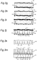
Figures 3a - 3m show schematically stages of a fabrication process of a sensing device of the present invention; -
Figure 4 shows a layout of a sensing circuit comprising the sensing device; -
Figures 5 - 8 show results of experiments with an exemplary sensing device according to the invention; -
Figure 9a and 9b show a layout of a sensing circuit comprising the sensing device in a respective embodiment; -
Figures 10, 11 show experimental results of an exemplary sensing device using the sensing circuit offigure 9a and 9b ; -
Figures 12a - 12c show perspective views of a sensing device in accordance with an embodiment of the invention; -
Figure 13 shows a schematic layout of the electrode structure of the bottom electrode of the sensing device offigure 12 ; -
Figure 14 shows a schematic layout of the structure of the top plate of the sensing device offigure 12 . - According to an embodiment, a force-
torque sensing device 1 comprises atop plate 3 with a planartop electrode structure 4, abottom plate 5 with a planarbottom electrode structure 6, and asupport structure 7. Thesupport structure 7 comprises spring elements for supporting thetop plate 3 on thebottom plate 5 with the planartop electrode structure 4 parallel to and facing the planarbottom electrode structure 6, seefigure 1a . The spring elements provide a gap G between the top andbottom electrode structures - The spring elements allow displacement of the
top plate 3 relative to thebottom plate 5 in three orthogonal directions X, Y, Z, two parallel (X,Y) and one perpendicular (Z) to thebottom plate 5, and for tilt of the top plate relative to the bottom plate around three orthogonal axes, corresponding with said two parallel and one perpendicular directions. In this manner, the force-torque sensing device is a so-called six axis detector capable of detecting forces in three orthogonal directions and moments around each of the axes parallel to these three directions. - In an embodiment, the force-torque sensor comprises a
silicon top plate 3 which is supported bythin silicon pillars 7. These pillars are the spring elements of the sensor for all degrees of freedom. - The silicon top plate forms the top electrode of the sensor that is placed on top of a semiconductor bottom plate that forms a bottom electrode.
- Under this top plate in the bottom plate, electrodes are created to measure the individual force and torque components using capacitive read-out.
- The spring elements arranged between the top plate and the bottom plate provide a gap G between the plates and allow that the top plate is moveable relative to the bottom plate. In this manner the electrodes in the top and bottom plate constitute a variable capacitor structure capable of measuring change in capacitance due to a change of position of the electrodes in the top part relative to the electrodes in the bottom part, i.e. a change in gap distance and/or a change of overlap area.
- A normal force Fz applied to the top plate will compress the silicon pillars and cause a change in gap proportional to the applied force, resulting in a changing capacitance, as shown in
Figure 1b . - To be able to measure moments Mx and My, the bottom electrode is divided into regions or area sections. In this exemplary configuration, four regions are used, to divide the bottom electrode into four quadrants each forming a capacitor with the top electrode.
- It will be appreciated that within the scope of the invention configurations with an other layout of regions are conceivable.
- Also, it will be appreciated that at least one electrode per degree of freedom is required. More electrodes per degree of freedom can increase the measurement sensitivity or improve the measurement accuracy.
- An applied moment Mx will cause a differential change in the gap between two opposite quadrants Q2, Q4 and therefore a differential change in capacitance, also shown in
Figure 1c . - For the measurement of shear forces Fx and Fy and moment Mz, comb-structures E1, E2, E3, E4 are integrated in the top and bottom electrode at the edges of each quadrant Q1, Q2, Q3, Q4, as shown in the plane view of
Figure 2a . - In the embodiment shown in
figure 2a ,pillars 7 are arranged along a two-dimensional lattice over the surface of the top and bottom electrode. - As shown in
figures 2b and 2c , a shear force Fx or Fy causes sideways bending of thesilicon pillars 7 and results in an in-plane translation d (Figure 2c ). As a result, differential changes in overlapping area occur between the upper and lower comb-structures U, L, resulting in a differential change in capacitance. - A moment Mz causes an in-plane rotation of the silicon top plate and results in sideways bending of the pillars radially around the axis of the applied moment. At the edges of the silicon top plate, the resulting translation causes a differential change in the comb-structures of all quadrants.
- The force range and mechanical sensitivity of the
sensing device 1 is controlled by the stiffness of the top plate support, which is determined by the number ofpillars 7, their length, their diameter and the mechanical properties of the pillars material. The number of pillars ranges from a minimum of one pillar up to the maximum pillars possible for the desired sensor area. The diameter of the pillars can range from e.g. 1 µm to the maximum size allowed by the desired sensor area. The electrical sensitivity can be controlled by the area of the electrodes and the gap distance. In this manner, the force-torque sensing device 1 can be scaled to adapt to a desired force/torque range and/or a desired sensitivity in each direction. - In an embodiment, the one or more pillars comprises a hollow cylinder.
- The following section describes a method for manufacturing the sensing device according to an embodiment. It will be appreciated that alternative fabrication methods for the sensor are conceivable.
- In the embodiment described here, silicon is chosen as the base material of the sensor, but also other materials such as polymers or ceramics can be used as top part and/or bottom part material.
- The sensor is fabricated using two
wafers top wafer 50 is a highly doped silicon wafer of 525 µm thickness, in which the silicon pillars are realized (Figure 3a ). - For the bottom wafer 51 a SOI wafer is used with a device layer of 25 µm, insulator thickness of 1 µm and a handle layer thickness of 380 µm, which is one of the possible configurations.
- The type and specific dimensions of the top and bottom wafer can be varied depending on the sensor requirements.
- For creating a
gap 53 between the electrodes, a slow reactive ion etching method is used withphotoresist 52 as mask (Fig. 3b,c ). Other methods, among which wet chemical etching can also be used to create thesmall gap 53. In this embodiment, the top side ofwafer 50 is also patterned (Fig. 3c ), to ensure that in the fabricated sensing device the load is guided through the silicon pillars to the lower wafer. - After etching the
gap 53, the photoresist mask is removed. (figure 3d ). - Deep reactive ion etching (DRIE) is one of the possible methods used to create the silicon pillars and to release the force sensitive surface from the wafer.
- In this embodiment, the silicon pillars need to be etched at a precisely controlled height and the release etch needs to be etched through the whole wafer.
- This is realized in a two-step DRIE process using a buried mask. The buried mask is created by depositing and patterning a silicon dioxide layer (TEOS) 54 of 1500 nm (
Fig. 3e,f ). This layer forms the mask for etching the silicon pillars. - The
TEOS layer 54 is covered with a patternedlayer 55 of OiR 907-17 photoresist (Fig. 3g ), which is used as a mask for releasing the force sensitive surface. - The first DRIE step etches 350 µm
deep trenches 56 to form the pre-release (Fig. 3h ). After this step, thephotoresist layer 55 is removed. - A
foil 57 is applied to the topside of the wafer, which is required for wafer-through etching (Fig. 3i ). This foil forms an etch stop and prevents leakage of the helium backside cooling and ensures stable temperature control of the wafer during the etching process. - In the second DRIE step, the
silicon pillars 7 are created by etching 300 µm deep 58 (Fig. 3j ). In this step, the force sensitive surface is released from thetop wafer substrate 50 and is only supported by its surrounding suspension. Thefoil 57 on the topside is removed with reactive O2 plasma (Tepla 300E) and the remaining (TEOS) oxide on the wafer is removed in a 50% HF solution (Fig. 3k ). - In the
bottom wafer 51,electrodes 59 andbond areas 60 are realized for capacitive read-out. An SOI-wafer is used to create the electrodes (Fig 3l ) and to enable high temperature silicon fusion bonding on thebond pads 60 with thepillars 7. - Fusion bonding is chosen to create a strong mechanical bond between the top and bottom wafer and is performed at 1100 °C, which makes the use of metal electrodes inapplicable in this embodiment.
- Both wafers undergo a 1% HF dip and are cleaned with fuming nitric acid (100%) and hot nitric acid (69%). Before bonding, the wafers are treated with a Piranha solution (H202:H2S04 = 1:3) for 30 minutes to clean the wafers and to create hydroxyl (OH) groups to initiate wafer bonding. Then, the wafers are aligned using a mask aligner and brought into contact to create a pre-bond. An IR-camera is used to monitor the pre-bond and then the wafers are exposed to 1100 °C in an N2 ambient for 7 hours to create a strong silicon-to-silicon bond (
Fig. 3m ). - In the method as described above, the electrodes U, L; E1, E2, E3, E4 consist of doped semiconductor material to allow the fusion bonding. It is noted that in alternative embodiments, where other manufacturing techniques are applied, the electrodes of the top and/or bottom part can be formed by a metal pattern on the surface of the top and/or bottom part substrates. To realize this, a bonding technique other than high temperature fusion bonding is required, e.g. eutectic, anodic or adhesive bonding.
- Additionally, the
sensing device 1 according to the invention may be manufactured from other materials than silicon, e.g. polymers or ceramics. - It is noted that in some embodiments, the material of choice for the top part may be different from the bottom part material. For example, a combination of silicon with a polymer or with glass is conceivable.
- As described above with reference with
figure 1b , a force Fz along the z-axis, i.e. perpendicular to the planar surface of thesensing device 1 is measured by change of the capacitance of the device due to change of the gap distance between top plate electrodes and bottom plate electrodes by the force F z. A moment Mz around the z-axis is measured by the change of capacitance due to a rotation of the top plate electrodes relative to the bottom plate electrodes causing a change in overlap area between top and bottom electrodes. The forces Fx, Fy parallel to the planar surface of the sensing device can be measured by change of capacitance by translation of the top plate electrodes relative to the bottom plate electrodes along the x-axis and y-axis respectively. Moments Mx, My cause a tilt of the top plate relative to the bottom plate around the x-axis and y-axis respectively, with a local change of the gap distance and can be measured accordingly by the corresponding change of capacitance. -
Figure 4 shows a layout of asensing circuit 11 comprising thesensing device 1. The top electrode U of thesensor 1 is connected to a charge amplifier 12 (Fig. 4 ) . For measuring moment Mx and My two opposite quadrants (e.g. Q1, Q3) are used that are measured in a parallel setting. On each quadrant, alternating (e.g. 1 MHz) voltage signals V1, V2 are applied to thelower electrodes 6 on the respective quadrant with 180° phase-shift with respect to each other. Using a charge amplifier results in an output signal V3 which is proportional to the differential change in capacitance between the two quadrants as caused by the applied force(s) and/or torque(s). Instead of connecting the common node of the differential capacitor directly to the input node of the sensing circuit, the connection may also be a capacitive connection through a coupling capacitor which may or may not be part of thesensing device 1. If the coupling capacitor is part of thesensing device 1 it may or may not be dependent on the measured forces and moments. - For the measurement of the shear force Fx the comb-structure pairs in Q2 and Q4 are used as differential input, for shear force Fy the comb-structure pairs in Q1 and Q3 are used. For the measurement of moment Mz all the comb-structure pairs can be combined.
-
Figure 5 shows an impedance output of asensing device 1 according to the invention measured with an impedance analyzer (e.g. HP 4194A) while loading and unloading in one cycle. -
Figure 6 shows an output of thesensor circuit 12 comprising thesensing device 1 according to the invention when a shear force Fx is applied. The output shows a differential capacitive measurement ΔC/C0 of the comb-structures E2, E4 (Cx) and E1, E3 (Cy). - To measure shear force or torque, the
differential charge amplifier 11 is connected to comb-structure pairs in the direction sensitive to force Fx (pairs E2 in Q2 and E4 in Q4). Due to the change in overlapping area in the comb-structure, the change in capacitance is directly proportional with the force Fx . The output of the channel orthogonal to the applied force (using pairs E1 in Q1 and E3 in Q3) is also plotted in the graph, showing a very low sensitivity for orthogonal forces. - In
Figure 7 , the output of the sensor according to the invention upon applying a moment My is shown. Two opposite quadrants Q1 and Q3 are connected in parallel to the charge amplifier measuring the differential change in capacitance between Q1 and Q3. An applied moment causes only a small change in angle between the top and bottom electrode. As a result, the differential change in capacitance is for small angle in approximation directly proportional to the applied moment. The output of the differential capacitive measurement of the charge amplifier in the orthogonal channel (Q2 and Q4) shows a very low sensitivity. - The output of the sensor in response to a moment Mz is shown in
figure 8 . Comb-structure pairs in Q1, Q2, Q3 and Q4 are connected such that a rotation around the z-axis causes a differential change in capacitance. A rotation around the center of the chip (i.e. the center between the comb structures E1, E2, E3and E4) causes a translation at the edges of the chip where the comb-structures are placed. This results in a linear relation of the change in capacitance with the applied moment. - Table 1 shows the range, full scale error and sensitivity of each individual axis for the sensing device as measured.
Table 1: Measured sensor performance Range %FSerror Sensitivity Fz 50 N 0.88 % 0.6 pF/N Fx 10N 0.43 % 0.01 pF/N Fy 10N 0.43 % 0.01 pF/N Mz 20 N·mm 2.76 % 0.01 pF/N·mm Mx 25 N·mm 1.13 % 1.3 pF/N·mm My 25 N-mm 1.13 % 1.3 pF/N·mm - Thus the present invention provides a design and realization of a six-degree of freedom force-torque sensor.
- In the embodiment, the sensor has a wide force range of up to 50 N in normal direction, 10 N in shear direction and 25 N-mm of maximum torque around each axis. By changing the number of pillars between the top plate and the bottom plate, their diameter and their length, the sensor can easily be scaled to adapt for other force/torque ranges and/or other sensitivities in each direction. The obtained accuracy, depending on the sensing axis, ranges from 0.43 % of full scale for the shear-force measurement to 2.8 % of full scale for Mz.
- In
figure 9a , asensing circuit 17 is shown that comprises thesensing device 1 as described above and that uses a type ofrelaxation oscillator 17 based on the per se known Modified Martin oscillator, to measure differential capacitance. Therelaxation oscillator 17 comprises the ModifiedMartin oscillator circuit 18, and a controllingunit 19. - For measuring forces and/or torques two opposite quadrants e.g. Q1, Q3 are used that are measured in a parallel setting. The
top electrode 20 of the sensor is connected to aninput node 22 of the relaxation oscillator. Theinput node 22 is also coupled by a reference capacitor Cref to an output of the controllingunit 19. Additionally, theoutput 18a of the Modified Martin oscillator is coupled to theinput 19a of the controllingunit 19. - As shown in
Figure 9a , two square-wave signals 23, 24 with opposite phase are fed to adifferential capacitor pair relaxation oscillator 17 is dependent on the differential capacitance, resulting in an output which is proportional to the differential change in capacitance between the two quadrants. - Instead of connecting the common node of the differential capacitor directly to the
input node 22 of the relaxation oscillator, the connection may also be a capacitive connection through a third capacitor as shown inFigure 9b . Here, one electrode of thefirst capacitor 25 and one electrode of thesecond capacitor 26 are electrically connected to each other and to one electrode of athird capacitor 30 comprising a third pair of a top electrode region and its corresponding bottom electrode region. The other electrode of the third capacitor is connected to theinput node 22 of the ModifiedMartin Oscillator 18. - Measuring each capacitance only involves switching of logic signals, which is performed by a CPLD (complex programmable logic device) in the controlling
unit 19. A microcontroller µC is used to measure the output frequency of therelaxation oscillator 17 for different capacitor configurations and determines the capacitance ratios. Capacitor Cref can be part of thesensing device 1 in order to compensate for e.g. variations in temperature. -
Figures 10 and 11 show experimental results of the change in frequency and the measured differential capacitance when a torque of up to 25 N.mm is applied. By sequentially switching capacitors, capacitance ratios are determined with a relatively high stability, in this experiment better than 60 ppm over a temperature range from 20°C to 50°C. -
Figure 10 shows an output frequency of theoscillator 17 while increasing the moment from 0 N-mm to 25 N·mm. (Csens indicates the frequency of the differential capacitance of two electrode regions in the sensing device 1). Three frequencies are measured to calculate the differential capacitance and to compensate for drift in the oscillator. -
Figure 11 shows a calculated differential capacitance from the frequencies infigure 10 . The offset as shown is caused by mismatch between the electrodes in the sensor. -
Figure 12a, 12b shows asensing device 1 according to an embodiment of the invention. In this embodiment, thesensing device 1 comprises a circular disk shapedtop part 23 which is connected to arigid ring 28 throughadditional spring elements 27 and supported by more than 300thin silicon pillars 7. A detailed cross-section of the circulartop part 23 is shown infigure 14 withtop electrode pattern 26. - The enclosing
ring 28 is rigidly attached to thebottom plate 25. - The
additional spring elements 27 between the enclosingring 28 and thetop plate 23 provide additional support of thetop part 23. Thespring elements 27 may comprise of a nest of springs of arbitrary shape. Additionally or alternatively, the spring elements may be embodied by a longitudinally elastically deformable (compressible and/or stretchable) and flexible membrane extending between thering 28 and thetop part 23. Optionally, this membrane may be corrugated. - Under the disk shaped
top part 23 withtop electrode pattern 26, circular electrodes are created 29 to measure the individual force components. -
Figure 13 shows a detailed embodiment ofbottom electrode pattern 29. An applied normal force Fz on thedisk 23 will compress the silicon pillars resulting in an out-of-plane displacement, as described above. This causes a change in gap G proportional to the applied force (figure 12b ). An applied shear force Fr will deform thespring elements 27 and bend the silicon pillars sideways, resulting in an in-plane displacement O proportional to the applied force. This causes a differential change in overlapping area between the top and bottom electrodes (figure 12c ). - As shown in
figure 13 , the displacement of the silicon disk can be measured capacitively using circular electrode pairs that are distributed in circular segments in four quadrants, in each quadrant Q1; Q2; Q3; Q4 the electrode pairs are distributed in an outer segment E11, E12; E21, E22; E31, E32; E41, E42 and an inner segment E13, E14; E23, E24; E33, E34; E43, E44. Within each segment the electrodes are interdigitated and of every pair of electrodes one electrode is connected to a first terminal T11, T13; T21, T23;T31, T33; T41, T43 and the other electrode is connected to a second terminal T12, T14; T22, T24;T32, T34; T42, T44. - In an example, a total of 96 concentric rings are divided in 8 segments (i.e. 4 quadrants, each quadrant having an inner segment and an outer segment) to measure shear force and normal force distribution.
- In an alternative embodiment as shown in
Figure 15 with a corresponding top electrode configuration, the electrode pairs can be straight, within each pair parallel to each other and oriented under 45° with the quadrant borders, while the electrode pairs are still arranged in inner and outer segments in each quadrant. This arrangement of the electrode pairs allows measurement of a moment Mz around the z-axis perpendicular to the plane of the electrode structures. - In embodiments with a plurality of electrode regions, the straight electrodes are oriented parallel to the bisector between the electrode region borders.
- The sensor may be fabricated using deep reactive ion etching to realize the corrugated silicon membrane forming the
spring elements 27 and thesilicon pillars 7 in the top part. - In an embodiment a method similar as the method explained with reference to
Figures 3a-3m can be applied. An SOI wafer is used to create the bottom electrodes and to enable high temperature fusion bonding which ensures a strong mechanical bond. The gap between the top and bottom electrode is created using etching or local oxidation of silicon. - After fabrication, the sensor is pushed out of the wafer, eliminating the need for dicing and allowing an arbitrary shape of the sensor chip. The sensor is typically mounted on a PCB complete with capacitive read-out electronics, consisting of the relaxation oscillator as described above with an output frequency proportional to differential capacitance.
- For measuring forces and/or torques two opposite quadrants e.g. Q1, Q3 are used that are measured in a parallel setting. The
top electrode 20 of the sensor is connected to aninput node 22 of the relaxation oscillator. Theinput node 22 is also coupled by a reference capacitor Cref to an output of the controllingunit 19. Additionally, theoutput 18a of the Modified Martin oscillator is coupled to theinput 19a of the controllingunit 19. - As shown in
Figure 9a , two square-wave signals 23, 24 with opposite phase are fed to adifferential capacitor pair relaxation oscillator 17 is dependent on the differential capacitance, resulting in an output which is proportional to the differential change in capacitance between the two quadrants. - Instead of connecting the common node of the differential capacitor directly to the
input node 22 of the relaxation oscillator, the connection may also be a capacitive connection through a third capacitor as shown inFigure 9b . Here, one electrode of thefirst capacitor 25 and one electrode of thesecond capacitor 26 are electrically connected to each other and to one electrode of athird capacitor 30 comprising a third pair of a top electrode region and its corresponding bottom electrode region. The other electrode of the third capacitor is connected to theinput node 22 of the ModifiedMartin Oscillator 18. - Measuring each capacitance only involves switching of logic signals, which is performed by a CPLD (complex programmable logic device) in the controlling
unit 19. A microcontroller µC is used to measure the output frequency of therelaxation oscillator 17 for different capacitor configurations and determines the capacitance ratios. Capacitor Cref can be part of thesensing device 1 in order to compensate for e.g. variations in temperature. -
Figures 10 and 11 show experimental results of the change in frequency and the measured differential capacitance when a torque of up to 25 N.mm is applied. By sequentially switching capacitors, capacitance ratios are determined with a relatively high stability, in this experiment better than 60 ppm over a temperature range from 20°C to 50°C. -
Figure 10 shows an output frequency of theoscillator 17 while increasing the moment from 0 N-mm to 25 N·mm. (Csens indicates the frequency of the differential capacitance of two electrode regions in the sensing device 1). Three frequencies are measured to calculate the differential capacitance and to compensate for drift in the oscillator. -
Figure 11 shows a calculated differential capacitance from the frequencies infigure 10 . The offset as shown is caused by mismatch between the electrodes in the sensor. -
Figure 12a, 12b shows asensing device 1 according to an embodiment of the invention. In this embodiment, thesensing device 1 comprises a circular disk shapedtop part 23 which is connected to arigid ring 28 throughadditional spring elements 27 and supported by more than 300thin silicon pillars 7. A detailed cross-section of the circulartop part 23 is shown infigure 14 withtop electrode pattern 26. - The enclosing
ring 28 is rigidly attached to thebottom plate 25. - The
additional spring elements 27 between the enclosingring 28 and thetop plate 23 provide additional support of thetop part 23. Thespring elements 27 may comprise of a nest of springs of arbitrary shape. Additionally or alternatively, the spring elements may be embodied by a longitudinally elastically deformable (compressible and/or stretchable) and flexible membrane extending between thering 28 and thetop part 23. Optionally, this membrane may be corrugated. - Under the disk shaped
top part 23 withtop electrode pattern 26, circular electrodes are created 29 to measure the individual force components. -
Figure 13 shows a detailed embodiment ofbottom electrode pattern 29. An applied normal force F z on thedisk 23 will compress the silicon pillars resulting in an out-of-plane displacement, as described above. This causes a change in gap G proportional to the applied force (figure 12b ). An applied shear force Fr will deform thespring elements 27 and bend the silicon pillars sideways, resulting in an in-plane displacement O proportional to the applied force. This causes a differential change in overlapping area between the top and bottom electrodes (figure 12c ). - As shown in
figure 13 , the displacement of the silicon disk can be measured capacitively using circular electrode pairs that are distributed in circular segments in four quadrants, in each quadrant Q1; Q2; Q3; Q4 the electrode pairs are distributed in an outer segment E11, E12; E21, E22; E31, E32; E41, E42 and an inner segment E13, E14; E23, E24; E33, E34; E43, E44. Within each segment the electrodes are interdigitated and of every pair of electrodes one electrode is connected to a first terminal T11, T13; T21, T23;T31, T33; T41, T43 and the other electrode is connected to a second terminal T12, T14; T22, T24;T32, T34; T42, T44. - In an example, a total of 96 concentric rings are divided in 8 segments (i.e. 4 quadrants, each quadrant having an inner segment and an outer segment) to measure shear force and normal force distribution.
- In an alternative embodiment as shown in
Figure 15 with a corresponding top electrode configuration, the electrode pairs can be straight, within each pair parallel to each other and oriented under 45° with the quadrant borders, while the electrode pairs are still arranged in inner and outer segments in each quadrant. This arrangement of the electrode pairs allows measurement of a moment Mz around the z-axis perpendicular to the plane of the electrode structures. - In embodiments with a plurality of electrode regions, the straight electrodes are oriented parallel to the bisector between the electrode region borders.
- The sensor may be fabricated using deep reactive ion etching to realize the corrugated silicon membrane forming the
spring elements 27 and thesilicon pillars 7 in the top part. - In an embodiment a method similar as the method explained with reference to
Figures 3a-3m can be applied. An SOI wafer is used to create the bottom electrodes and to enable high temperature fusion bonding which ensures a strong mechanical bond. The gap between the top and bottom electrode is created using etching or local oxidation of silicon. - After fabrication, the sensor is pushed out of the wafer, eliminating the need for dicing and allowing an arbitrary shape of the sensor chip. The sensor is typically mounted on a PCB complete with capacitive read-out electronics, consisting of the relaxation oscillator as described above with an output frequency proportional to differential capacitance.
Claims (14)
- A sensing device (1) for measuring force and/or torque
comprising a top part (3; 23) with a top electrode structure (4; 26), a bottom part (5; 25) with a bottom electrode structure (6; 29), and a support structure;
the support structure comprising spring elements for supporting the top part on the bottom part with the top electrode structure parallel to and facing the bottom electrode structure, the spring elements arranged for providing a gap (G) between the top and bottom electrode structures;
the spring elements being arranged for allowing displacement of the top part relative to the bottom part in three orthogonal directions (X, Y, Z) two parallel and one perpendicular to the bottom part, and for rotation of the top part relative to the bottom part around three orthogonal axes, corresponding with said two parallel and one perpendicular directions (X, Y, Z); the top and bottom electrode structures being located in positions on the top and the bottom part, respectively, and positioned in such a way that a change in distance between and/or a change in overlap area of the top and bottom electrodes and a corresponding change of capacitance are induced by the displacement and/or rotation of the top and bottom electrode structures relative to each other,
characterised in that each spring element comprises at least one pillar (7), each pillar is arranged to be both longitudinally deformable and transversely flexible, each pillar provides a mechanical coupling of the top part (3) to the bottom part (5),
and the pillars (7) are arranged along a two-dimensional lattice over the surface of the top and bottom electrode (4; 6). - The sensing device (1) according to claim 1, wherein the top and bottom electrode structures (4, 6; 26, 29) comprise one or more electrode pairs (E1; E2; E3; E4), for each of the force components that are measured.
- The sensing device (1) according to claim 1 or claim 2, wherein the bottom electrode structure (6) comprises a plurality of bottom electrode regions (Q1, Q2, Q3, Q4) around a center (C) of the bottom electrode structure.
- The sensing device (1) according to claim 3, wherein the bottom electrode structure comprises four bottom electrode regions configured in quadrants and a top electrode region comprises a top comb structure (U) at the outer edge of each quadrant, and
each bottom electrode region comprises a bottom comb structure (L) at the outer edge of the respective corresponding quadrant. - The sensing device (1) according to claim 1, wherein the pillars form part of either the top part or the bottom part or both parts and extend above or below the electrode structure in the respective part.
- The sensing device (1) according to any of the preceding claims wherein the sensing device comprises an enclosing part (28) surrounding one of the top part (23) and the bottom part (25) and being attached to the other of the top part and the bottom part,
and one or more additional spring elements (27) is coupled between said enclosing part (28) and said one (23; 25) of the top and the bottom part in order to provide additional support. - The sensing device (1) according to claim 6, wherein the one or more additional spring elements (27) comprise a membrane between said enclosing part and said one of the top and the bottom part, the membrane being longitudinally deformable and transversely flexible.
- The sensing device (1) according to claim 7, wherein the membrane is corrugated.
- The sensing device (1) according to claim 1, wherein the top part and/or the bottom part is a semiconductor-based plate.
- The sensing device (1) according to claim 9, wherein the bottom part is a doped silicon-on-insulator plate (51).
- The sensing device (1) according to claims 10, wherein
the pillars are silicon based, form part of either the top part or bottom part or both, and couple the top part and the bottom part. - The sensing device (1) according to claim 9, wherein the top electrode structure and/or the bottom electrode structure (U, L; E1, E2, E3, E4) comprises a metal pattern.
- The sensing device (1) according to claim 12, wherein the top part and/or the bottom part comprises an insulating support layer supporting respectively the top electrode and/or the bottom electrode structure (U, L; E1, E2, E3, E4).
- The sensing device (1) according to claim 3 or claim 4, wherein the bottom electrode regions (Q1, Q2, Q3, Q4) configured around the center (C) of the electrode structure comprise elongated substantially straight electrodes (E11, E12, E13, E14) running from the center of the electrode structure to a periphery of the electrode structure, wherein each region (Q1; Q2; Q3; Q4) comprises an inner segment with first elongated electrodes (E13, E14) and an outer segment with second elongated electrodes (E11, E12);
within each segment the electrodes are interdigitated and connected to separate terminals (T11, T13; T21, T23; T31, T33; T41, T43; T12, T14; T22, T24; T32, T34; T42, T44).
Applications Claiming Priority (2)
| Application Number | Priority Date | Filing Date | Title |
|---|---|---|---|
| US201261585727P | 2012-01-12 | 2012-01-12 | |
| PCT/NL2013/050017 WO2013105859A2 (en) | 2012-01-12 | 2013-01-14 | Six-axis force-torque sensor |
Publications (2)
| Publication Number | Publication Date |
|---|---|
| EP2802851A2 EP2802851A2 (en) | 2014-11-19 |
| EP2802851B1 true EP2802851B1 (en) | 2020-08-19 |
Family
ID=47716139
Family Applications (1)
| Application Number | Title | Priority Date | Filing Date |
|---|---|---|---|
| EP13704501.9A Active EP2802851B1 (en) | 2012-01-12 | 2013-01-14 | Six-axis force-torque sensor |
Country Status (3)
| Country | Link |
|---|---|
| US (1) | US9423308B2 (en) |
| EP (1) | EP2802851B1 (en) |
| WO (1) | WO2013105859A2 (en) |
Families Citing this family (23)
| Publication number | Priority date | Publication date | Assignee | Title |
|---|---|---|---|---|
| CN103776578B (en) * | 2014-02-20 | 2016-01-06 | 哈尔滨工业大学(威海) | A kind of force on cross-section survey sensor and scaling method |
| US9952252B2 (en) * | 2015-05-15 | 2018-04-24 | Invensense, Inc. | Offset rejection electrodes |
| US11231441B2 (en) * | 2015-05-15 | 2022-01-25 | Invensense, Inc. | MEMS structure for offset minimization of out-of-plane sensing accelerometers |
| TWI575232B (en) * | 2015-06-12 | 2017-03-21 | 財團法人工業技術研究院 | Sensing device |
| CN105973521B (en) * | 2016-07-08 | 2019-03-08 | 中国电子科技集团公司第二十一研究所 | 3D pressure sensor |
| CN106017769B (en) * | 2016-07-08 | 2018-12-28 | 燕山大学 | A kind of deformable Three-Dimensional Dynamic force snesor in parallel |
| JP6431005B2 (en) * | 2016-07-13 | 2018-11-28 | ファナック株式会社 | Sensor device |
| KR102330396B1 (en) * | 2016-12-02 | 2021-11-24 | 주식회사 로보터스 | Capacitive sensor |
| CN106840472B (en) * | 2017-01-12 | 2019-08-13 | 东南大学 | A kind of high-precision three-dimensional soil pressure testing device and its range adjust system |
| JP6626074B2 (en) * | 2017-11-28 | 2019-12-25 | ファナック株式会社 | Displacement detection type force detection structure and force sensor |
| JP6626075B2 (en) * | 2017-11-28 | 2019-12-25 | ファナック株式会社 | 6-axis displacement sensor with displacement detection |
| EP3495826B1 (en) * | 2017-12-07 | 2020-11-25 | EM Microelectronic-Marin SA | Electronic device for measuring a physical parameter |
| CN108693382B (en) * | 2018-04-28 | 2020-05-15 | 北京林业大学 | A parallel six-dimensional acceleration sensor |
| JP7145042B2 (en) * | 2018-11-08 | 2022-09-30 | 東京エレクトロン株式会社 | Substrate support and plasma processing equipment |
| WO2020097730A1 (en) * | 2018-11-16 | 2020-05-22 | The University Of British Columbia | Deformable sensor for simulating skin and other applications |
| EP3705861B1 (en) | 2019-03-08 | 2021-05-12 | Infineon Technologies AG | Sensor with a membrane electrode, a counterelectrode, and at least one spring |
| CN112611497B (en) * | 2019-09-18 | 2022-01-28 | 马洪文 | Multi-dimensional force sensor structure of parallel rod system |
| CN112611498B (en) * | 2019-09-18 | 2022-02-01 | 马洪文 | Multi-dimensional force acquisition method based on multi-dimensional force sensor of parallel rod system |
| CN110579304A (en) * | 2019-10-17 | 2019-12-17 | 广西大学 | A Differential Capacitive Multidimensional Force Sensor |
| JP7560031B2 (en) * | 2021-01-20 | 2024-10-02 | 本田技研工業株式会社 | 3-axis force sensor |
| CN113916433B (en) * | 2021-09-01 | 2024-04-19 | 杭州电子科技大学 | High-sensitivity three-dimensional force and moment decoupling touch sensor structure |
| CN114323396B (en) * | 2021-12-23 | 2022-11-11 | 西安交通大学 | MEMS capacitive six-axis force sensor chip and preparation process thereof |
| WO2025052627A1 (en) * | 2023-09-07 | 2025-03-13 | 株式会社 トライフォース・マネジメント | Force sensor |
Citations (2)
| Publication number | Priority date | Publication date | Assignee | Title |
|---|---|---|---|---|
| JP2010223953A (en) * | 2009-02-26 | 2010-10-07 | Tokai Rubber Ind Ltd | Capacitance-type pressure-sensitive sensor and manufacturing method thereof |
| JP2011128096A (en) * | 2009-12-21 | 2011-06-30 | Wacoh Corp | Displacement sensor and force detector |
Family Cites Families (10)
| Publication number | Priority date | Publication date | Assignee | Title |
|---|---|---|---|---|
| US4585082A (en) * | 1984-08-17 | 1986-04-29 | Harrington Richard H | Weight scale utilizing a capacitative load cell |
| US6820493B1 (en) * | 1999-10-06 | 2004-11-23 | Wayne Bonin | Precision multi-dimensional capacitive transducer |
| US7088492B2 (en) * | 2001-10-11 | 2006-08-08 | Denso Corporation | Micro movable mechanism system and control method for the same |
| FI119528B (en) * | 2003-02-11 | 2008-12-15 | Vti Technologies Oy | Capacitive accelerometer design |
| JP4271475B2 (en) * | 2003-03-31 | 2009-06-03 | 株式会社ワコー | Force detection device |
| US7047818B2 (en) * | 2003-04-09 | 2006-05-23 | Loadstar Sensors, Inc. | Capacitive force sensing device |
| US7443569B2 (en) * | 2003-04-24 | 2008-10-28 | Jds Uniphase Corporation | Micro-electro-mechanical-system two dimensional mirror with articulated suspension structures for high fill factor arrays |
| US20100268121A1 (en) * | 2009-03-18 | 2010-10-21 | Kilborn John C | Active support surface |
| JP5439068B2 (en) | 2009-07-08 | 2014-03-12 | 株式会社ワコー | Force detection device |
| US9470709B2 (en) * | 2013-01-28 | 2016-10-18 | Analog Devices, Inc. | Teeter totter accelerometer with unbalanced mass |
-
2013
- 2013-01-14 US US14/371,632 patent/US9423308B2/en active Active
- 2013-01-14 WO PCT/NL2013/050017 patent/WO2013105859A2/en not_active Ceased
- 2013-01-14 EP EP13704501.9A patent/EP2802851B1/en active Active
Patent Citations (2)
| Publication number | Priority date | Publication date | Assignee | Title |
|---|---|---|---|---|
| JP2010223953A (en) * | 2009-02-26 | 2010-10-07 | Tokai Rubber Ind Ltd | Capacitance-type pressure-sensitive sensor and manufacturing method thereof |
| JP2011128096A (en) * | 2009-12-21 | 2011-06-30 | Wacoh Corp | Displacement sensor and force detector |
Also Published As
| Publication number | Publication date |
|---|---|
| WO2013105859A2 (en) | 2013-07-18 |
| US20140331787A1 (en) | 2014-11-13 |
| WO2013105859A3 (en) | 2013-11-07 |
| EP2802851A2 (en) | 2014-11-19 |
| US9423308B2 (en) | 2016-08-23 |
Similar Documents
| Publication | Publication Date | Title |
|---|---|---|
| US9423308B2 (en) | Six-axis force-torque sensor | |
| US7360455B2 (en) | Force detector and acceleration detector and method of manufacturing the same | |
| JP5638598B2 (en) | Vertically integrated MEMS acceleration transducer | |
| US6158291A (en) | Force detector and acceleration detector | |
| US6201284B1 (en) | Multi-axis acceleration sensor and manufacturing method thereof | |
| JP2012225920A (en) | Micro-electromechanical system (mems) device | |
| CN102128953B (en) | Capacitive micro-accelerometer with symmetrical tilted folded beam structure | |
| Brookhuis et al. | 3D force sensor for biomechanical applications | |
| EP3307671A1 (en) | Ruggedized wafer level mems force sensor with a tolerance trench | |
| JP4335545B2 (en) | Sensor for detecting both pressure and acceleration and manufacturing method thereof | |
| US9511993B2 (en) | Semiconductor physical quantity detecting sensor | |
| CN114323396B (en) | MEMS capacitive six-axis force sensor chip and preparation process thereof | |
| US20180162723A1 (en) | Inertia sensor | |
| JP6258977B2 (en) | Sensor and manufacturing method thereof | |
| Brookhuis et al. | Scalable six-axis force-torque sensor with a large range for biomechanical applications | |
| Brookhuis et al. | Large range multi-axis fingertip force sensor | |
| CN108253882A (en) | A kind of angle measurement unit of micro motor | |
| Hata et al. | An SOI tactile sensor with a quad seesaw electrode for 3-axis complete differential detection | |
| JP4089961B2 (en) | Acceleration sensor | |
| JPH04249726A (en) | Manufacture for sensor utilizing change of electrostatic capacity | |
| Brookhuis et al. | Three-axis force-torque sensor with fully differential capacitive readout | |
| JP2971610B2 (en) | Force / acceleration / magnetism detecting device and method of manufacturing the same | |
| Brookhuis et al. | Six-axis force-torque sensor | |
| JP4056591B2 (en) | Acceleration sensor | |
| JPH07225243A (en) | Acceleration sensor and manufacturing method thereof, acceleration detection method using the acceleration sensor, and acceleration sensor array |
Legal Events
| Date | Code | Title | Description |
|---|---|---|---|
| PUAI | Public reference made under article 153(3) epc to a published international application that has entered the european phase |
Free format text: ORIGINAL CODE: 0009012 |
|
| 17P | Request for examination filed |
Effective date: 20140722 |
|
| AK | Designated contracting states |
Kind code of ref document: A2 Designated state(s): AL AT BE BG CH CY CZ DE DK EE ES FI FR GB GR HR HU IE IS IT LI LT LU LV MC MK MT NL NO PL PT RO RS SE SI SK SM TR |
|
| DAX | Request for extension of the european patent (deleted) | ||
| STAA | Information on the status of an ep patent application or granted ep patent |
Free format text: STATUS: EXAMINATION IS IN PROGRESS |
|
| 17Q | First examination report despatched |
Effective date: 20170404 |
|
| RIC1 | Information provided on ipc code assigned before grant |
Ipc: G01P 15/125 20060101AFI20190510BHEP Ipc: G01L 3/02 20060101ALI20190510BHEP Ipc: G01R 27/26 20060101ALI20190510BHEP Ipc: G01L 1/14 20060101ALI20190510BHEP Ipc: G01L 5/16 20060101ALI20190510BHEP |
|
| GRAP | Despatch of communication of intention to grant a patent |
Free format text: ORIGINAL CODE: EPIDOSNIGR1 |
|
| STAA | Information on the status of an ep patent application or granted ep patent |
Free format text: STATUS: GRANT OF PATENT IS INTENDED |
|
| INTG | Intention to grant announced |
Effective date: 20191119 |
|
| GRAJ | Information related to disapproval of communication of intention to grant by the applicant or resumption of examination proceedings by the epo deleted |
Free format text: ORIGINAL CODE: EPIDOSDIGR1 |
|
| STAA | Information on the status of an ep patent application or granted ep patent |
Free format text: STATUS: EXAMINATION IS IN PROGRESS |
|
| REG | Reference to a national code |
Ref country code: DE Ref legal event code: R079 Ref document number: 602013071735 Country of ref document: DE Free format text: PREVIOUS MAIN CLASS: G01L0001140000 Ipc: G01L0005165000 |
|
| GRAP | Despatch of communication of intention to grant a patent |
Free format text: ORIGINAL CODE: EPIDOSNIGR1 |
|
| STAA | Information on the status of an ep patent application or granted ep patent |
Free format text: STATUS: GRANT OF PATENT IS INTENDED |
|
| INTC | Intention to grant announced (deleted) | ||
| RIC1 | Information provided on ipc code assigned before grant |
Ipc: G01L 1/14 20060101ALI20200218BHEP Ipc: G01L 5/165 20200101AFI20200218BHEP |
|
| INTG | Intention to grant announced |
Effective date: 20200313 |
|
| GRAS | Grant fee paid |
Free format text: ORIGINAL CODE: EPIDOSNIGR3 |
|
| GRAA | (expected) grant |
Free format text: ORIGINAL CODE: 0009210 |
|
| STAA | Information on the status of an ep patent application or granted ep patent |
Free format text: STATUS: THE PATENT HAS BEEN GRANTED |
|
| AK | Designated contracting states |
Kind code of ref document: B1 Designated state(s): AL AT BE BG CH CY CZ DE DK EE ES FI FR GB GR HR HU IE IS IT LI LT LU LV MC MK MT NL NO PL PT RO RS SE SI SK SM TR |
|
| REG | Reference to a national code |
Ref country code: GB Ref legal event code: FG4D |
|
| REG | Reference to a national code |
Ref country code: CH Ref legal event code: EP |
|
| REG | Reference to a national code |
Ref country code: DE Ref legal event code: R096 Ref document number: 602013071735 Country of ref document: DE |
|
| REG | Reference to a national code |
Ref country code: AT Ref legal event code: REF Ref document number: 1304473 Country of ref document: AT Kind code of ref document: T Effective date: 20200915 |
|
| REG | Reference to a national code |
Ref country code: IE Ref legal event code: FG4D |
|
| REG | Reference to a national code |
Ref country code: NL Ref legal event code: FP |
|
| REG | Reference to a national code |
Ref country code: LT Ref legal event code: MG4D |
|
| PG25 | Lapsed in a contracting state [announced via postgrant information from national office to epo] |
Ref country code: GR Free format text: LAPSE BECAUSE OF FAILURE TO SUBMIT A TRANSLATION OF THE DESCRIPTION OR TO PAY THE FEE WITHIN THE PRESCRIBED TIME-LIMIT Effective date: 20201120 Ref country code: BG Free format text: LAPSE BECAUSE OF FAILURE TO SUBMIT A TRANSLATION OF THE DESCRIPTION OR TO PAY THE FEE WITHIN THE PRESCRIBED TIME-LIMIT Effective date: 20201119 Ref country code: HR Free format text: LAPSE BECAUSE OF FAILURE TO SUBMIT A TRANSLATION OF THE DESCRIPTION OR TO PAY THE FEE WITHIN THE PRESCRIBED TIME-LIMIT Effective date: 20200819 Ref country code: LT Free format text: LAPSE BECAUSE OF FAILURE TO SUBMIT A TRANSLATION OF THE DESCRIPTION OR TO PAY THE FEE WITHIN THE PRESCRIBED TIME-LIMIT Effective date: 20200819 Ref country code: PT Free format text: LAPSE BECAUSE OF FAILURE TO SUBMIT A TRANSLATION OF THE DESCRIPTION OR TO PAY THE FEE WITHIN THE PRESCRIBED TIME-LIMIT Effective date: 20201221 Ref country code: FI Free format text: LAPSE BECAUSE OF FAILURE TO SUBMIT A TRANSLATION OF THE DESCRIPTION OR TO PAY THE FEE WITHIN THE PRESCRIBED TIME-LIMIT Effective date: 20200819 Ref country code: SE Free format text: LAPSE BECAUSE OF FAILURE TO SUBMIT A TRANSLATION OF THE DESCRIPTION OR TO PAY THE FEE WITHIN THE PRESCRIBED TIME-LIMIT Effective date: 20200819 Ref country code: NO Free format text: LAPSE BECAUSE OF FAILURE TO SUBMIT A TRANSLATION OF THE DESCRIPTION OR TO PAY THE FEE WITHIN THE PRESCRIBED TIME-LIMIT Effective date: 20201119 |
|
| REG | Reference to a national code |
Ref country code: AT Ref legal event code: MK05 Ref document number: 1304473 Country of ref document: AT Kind code of ref document: T Effective date: 20200819 |
|
| PG25 | Lapsed in a contracting state [announced via postgrant information from national office to epo] |
Ref country code: IS Free format text: LAPSE BECAUSE OF FAILURE TO SUBMIT A TRANSLATION OF THE DESCRIPTION OR TO PAY THE FEE WITHIN THE PRESCRIBED TIME-LIMIT Effective date: 20201219 Ref country code: LV Free format text: LAPSE BECAUSE OF FAILURE TO SUBMIT A TRANSLATION OF THE DESCRIPTION OR TO PAY THE FEE WITHIN THE PRESCRIBED TIME-LIMIT Effective date: 20200819 Ref country code: PL Free format text: LAPSE BECAUSE OF FAILURE TO SUBMIT A TRANSLATION OF THE DESCRIPTION OR TO PAY THE FEE WITHIN THE PRESCRIBED TIME-LIMIT Effective date: 20200819 Ref country code: RS Free format text: LAPSE BECAUSE OF FAILURE TO SUBMIT A TRANSLATION OF THE DESCRIPTION OR TO PAY THE FEE WITHIN THE PRESCRIBED TIME-LIMIT Effective date: 20200819 |
|
| PG25 | Lapsed in a contracting state [announced via postgrant information from national office to epo] |
Ref country code: RO Free format text: LAPSE BECAUSE OF FAILURE TO SUBMIT A TRANSLATION OF THE DESCRIPTION OR TO PAY THE FEE WITHIN THE PRESCRIBED TIME-LIMIT Effective date: 20200819 Ref country code: SM Free format text: LAPSE BECAUSE OF FAILURE TO SUBMIT A TRANSLATION OF THE DESCRIPTION OR TO PAY THE FEE WITHIN THE PRESCRIBED TIME-LIMIT Effective date: 20200819 Ref country code: DK Free format text: LAPSE BECAUSE OF FAILURE TO SUBMIT A TRANSLATION OF THE DESCRIPTION OR TO PAY THE FEE WITHIN THE PRESCRIBED TIME-LIMIT Effective date: 20200819 Ref country code: CZ Free format text: LAPSE BECAUSE OF FAILURE TO SUBMIT A TRANSLATION OF THE DESCRIPTION OR TO PAY THE FEE WITHIN THE PRESCRIBED TIME-LIMIT Effective date: 20200819 Ref country code: EE Free format text: LAPSE BECAUSE OF FAILURE TO SUBMIT A TRANSLATION OF THE DESCRIPTION OR TO PAY THE FEE WITHIN THE PRESCRIBED TIME-LIMIT Effective date: 20200819 |
|
| REG | Reference to a national code |
Ref country code: DE Ref legal event code: R097 Ref document number: 602013071735 Country of ref document: DE |
|
| PG25 | Lapsed in a contracting state [announced via postgrant information from national office to epo] |
Ref country code: ES Free format text: LAPSE BECAUSE OF FAILURE TO SUBMIT A TRANSLATION OF THE DESCRIPTION OR TO PAY THE FEE WITHIN THE PRESCRIBED TIME-LIMIT Effective date: 20200819 Ref country code: AT Free format text: LAPSE BECAUSE OF FAILURE TO SUBMIT A TRANSLATION OF THE DESCRIPTION OR TO PAY THE FEE WITHIN THE PRESCRIBED TIME-LIMIT Effective date: 20200819 Ref country code: AL Free format text: LAPSE BECAUSE OF FAILURE TO SUBMIT A TRANSLATION OF THE DESCRIPTION OR TO PAY THE FEE WITHIN THE PRESCRIBED TIME-LIMIT Effective date: 20200819 |
|
| PLBE | No opposition filed within time limit |
Free format text: ORIGINAL CODE: 0009261 |
|
| STAA | Information on the status of an ep patent application or granted ep patent |
Free format text: STATUS: NO OPPOSITION FILED WITHIN TIME LIMIT |
|
| PG25 | Lapsed in a contracting state [announced via postgrant information from national office to epo] |
Ref country code: SK Free format text: LAPSE BECAUSE OF FAILURE TO SUBMIT A TRANSLATION OF THE DESCRIPTION OR TO PAY THE FEE WITHIN THE PRESCRIBED TIME-LIMIT Effective date: 20200819 |
|
| 26N | No opposition filed |
Effective date: 20210520 |
|
| PG25 | Lapsed in a contracting state [announced via postgrant information from national office to epo] |
Ref country code: IT Free format text: LAPSE BECAUSE OF FAILURE TO SUBMIT A TRANSLATION OF THE DESCRIPTION OR TO PAY THE FEE WITHIN THE PRESCRIBED TIME-LIMIT Effective date: 20200819 |
|
| PG25 | Lapsed in a contracting state [announced via postgrant information from national office to epo] |
Ref country code: SI Free format text: LAPSE BECAUSE OF FAILURE TO SUBMIT A TRANSLATION OF THE DESCRIPTION OR TO PAY THE FEE WITHIN THE PRESCRIBED TIME-LIMIT Effective date: 20200819 Ref country code: MC Free format text: LAPSE BECAUSE OF FAILURE TO SUBMIT A TRANSLATION OF THE DESCRIPTION OR TO PAY THE FEE WITHIN THE PRESCRIBED TIME-LIMIT Effective date: 20200819 |
|
| PG25 | Lapsed in a contracting state [announced via postgrant information from national office to epo] |
Ref country code: LU Free format text: LAPSE BECAUSE OF NON-PAYMENT OF DUE FEES Effective date: 20210114 |
|
| PG25 | Lapsed in a contracting state [announced via postgrant information from national office to epo] |
Ref country code: IE Free format text: LAPSE BECAUSE OF NON-PAYMENT OF DUE FEES Effective date: 20210114 |
|
| PG25 | Lapsed in a contracting state [announced via postgrant information from national office to epo] |
Ref country code: HU Free format text: LAPSE BECAUSE OF FAILURE TO SUBMIT A TRANSLATION OF THE DESCRIPTION OR TO PAY THE FEE WITHIN THE PRESCRIBED TIME-LIMIT; INVALID AB INITIO Effective date: 20130114 |
|
| PG25 | Lapsed in a contracting state [announced via postgrant information from national office to epo] |
Ref country code: CY Free format text: LAPSE BECAUSE OF FAILURE TO SUBMIT A TRANSLATION OF THE DESCRIPTION OR TO PAY THE FEE WITHIN THE PRESCRIBED TIME-LIMIT Effective date: 20200819 |
|
| P01 | Opt-out of the competence of the unified patent court (upc) registered |
Effective date: 20230601 |
|
| PG25 | Lapsed in a contracting state [announced via postgrant information from national office to epo] |
Ref country code: MK Free format text: LAPSE BECAUSE OF FAILURE TO SUBMIT A TRANSLATION OF THE DESCRIPTION OR TO PAY THE FEE WITHIN THE PRESCRIBED TIME-LIMIT Effective date: 20200819 |
|
| PG25 | Lapsed in a contracting state [announced via postgrant information from national office to epo] |
Ref country code: TR Free format text: LAPSE BECAUSE OF FAILURE TO SUBMIT A TRANSLATION OF THE DESCRIPTION OR TO PAY THE FEE WITHIN THE PRESCRIBED TIME-LIMIT Effective date: 20200819 |
|
| PG25 | Lapsed in a contracting state [announced via postgrant information from national office to epo] |
Ref country code: MT Free format text: LAPSE BECAUSE OF FAILURE TO SUBMIT A TRANSLATION OF THE DESCRIPTION OR TO PAY THE FEE WITHIN THE PRESCRIBED TIME-LIMIT Effective date: 20200819 |
|
| PGFP | Annual fee paid to national office [announced via postgrant information from national office to epo] |
Ref country code: NL Payment date: 20250110 Year of fee payment: 13 |
|
| PGFP | Annual fee paid to national office [announced via postgrant information from national office to epo] |
Ref country code: DE Payment date: 20250129 Year of fee payment: 13 |
|
| PGFP | Annual fee paid to national office [announced via postgrant information from national office to epo] |
Ref country code: CH Payment date: 20250201 Year of fee payment: 13 Ref country code: BE Payment date: 20250127 Year of fee payment: 13 |
|
| PGFP | Annual fee paid to national office [announced via postgrant information from national office to epo] |
Ref country code: FR Payment date: 20250127 Year of fee payment: 13 |
|
| PGFP | Annual fee paid to national office [announced via postgrant information from national office to epo] |
Ref country code: GB Payment date: 20250121 Year of fee payment: 13 |