EP2802074B1 - Circuit amplificateur et procédé d'amplification - Google Patents
Circuit amplificateur et procédé d'amplification Download PDFInfo
- Publication number
- EP2802074B1 EP2802074B1 EP13167118.2A EP13167118A EP2802074B1 EP 2802074 B1 EP2802074 B1 EP 2802074B1 EP 13167118 A EP13167118 A EP 13167118A EP 2802074 B1 EP2802074 B1 EP 2802074B1
- Authority
- EP
- European Patent Office
- Prior art keywords
- output
- circuit
- amplifier
- gain
- analogue
- Prior art date
- Legal status (The legal status is an assumption and is not a legal conclusion. Google has not performed a legal analysis and makes no representation as to the accuracy of the status listed.)
- Active
Links
Images

Classifications
-
- H—ELECTRICITY
- H03—ELECTRONIC CIRCUITRY
- H03F—AMPLIFIERS
- H03F3/00—Amplifiers with only discharge tubes or only semiconductor devices as amplifying elements
- H03F3/45—Differential amplifiers
- H03F3/45071—Differential amplifiers with semiconductor devices only
- H03F3/45479—Differential amplifiers with semiconductor devices only characterised by the way of common mode signal rejection
- H03F3/45928—Differential amplifiers with semiconductor devices only characterised by the way of common mode signal rejection using IC blocks as the active amplifying circuit
- H03F3/45968—Differential amplifiers with semiconductor devices only characterised by the way of common mode signal rejection using IC blocks as the active amplifying circuit by offset reduction
- H03F3/45973—Differential amplifiers with semiconductor devices only characterised by the way of common mode signal rejection using IC blocks as the active amplifying circuit by offset reduction by using a feedback circuit
-
- H—ELECTRICITY
- H03—ELECTRONIC CIRCUITRY
- H03G—CONTROL OF AMPLIFICATION
- H03G3/00—Gain control in amplifiers or frequency changers without distortion of the input signal
- H03G3/20—Automatic control
- H03G3/30—Automatic control in amplifiers having semiconductor devices
- H03G3/3005—Automatic control in amplifiers having semiconductor devices in amplifiers suitable for low-frequencies, e.g. audio amplifiers
- H03G3/301—Automatic control in amplifiers having semiconductor devices in amplifiers suitable for low-frequencies, e.g. audio amplifiers the gain being continuously variable
-
- G—PHYSICS
- G07—CHECKING-DEVICES
- G07C—TIME OR ATTENDANCE REGISTERS; REGISTERING OR INDICATING THE WORKING OF MACHINES; GENERATING RANDOM NUMBERS; VOTING OR LOTTERY APPARATUS; ARRANGEMENTS, SYSTEMS OR APPARATUS FOR CHECKING NOT PROVIDED FOR ELSEWHERE
- G07C9/00—Individual registration on entry or exit
- G07C9/00174—Electronically operated locks; Circuits therefor; Nonmechanical keys therefor, e.g. passive or active electrical keys or other data carriers without mechanical keys
- G07C9/00309—Electronically operated locks; Circuits therefor; Nonmechanical keys therefor, e.g. passive or active electrical keys or other data carriers without mechanical keys operated with bidirectional data transmission between data carrier and locks
-
- G—PHYSICS
- G07—CHECKING-DEVICES
- G07C—TIME OR ATTENDANCE REGISTERS; REGISTERING OR INDICATING THE WORKING OF MACHINES; GENERATING RANDOM NUMBERS; VOTING OR LOTTERY APPARATUS; ARRANGEMENTS, SYSTEMS OR APPARATUS FOR CHECKING NOT PROVIDED FOR ELSEWHERE
- G07C9/00—Individual registration on entry or exit
- G07C9/00174—Electronically operated locks; Circuits therefor; Nonmechanical keys therefor, e.g. passive or active electrical keys or other data carriers without mechanical keys
- G07C9/00571—Electronically operated locks; Circuits therefor; Nonmechanical keys therefor, e.g. passive or active electrical keys or other data carriers without mechanical keys operated by interacting with a central unit
-
- H—ELECTRICITY
- H03—ELECTRONIC CIRCUITRY
- H03F—AMPLIFIERS
- H03F1/00—Details of amplifiers with only discharge tubes, only semiconductor devices or only unspecified devices as amplifying elements
- H03F1/30—Modifications of amplifiers to reduce influence of variations of temperature or supply voltage or other physical parameters
- H03F1/305—Modifications of amplifiers to reduce influence of variations of temperature or supply voltage or other physical parameters in case of switching on or off of a power supply
-
- H—ELECTRICITY
- H03—ELECTRONIC CIRCUITRY
- H03F—AMPLIFIERS
- H03F3/00—Amplifiers with only discharge tubes or only semiconductor devices as amplifying elements
- H03F3/181—Low frequency amplifiers, e.g. audio preamplifiers
- H03F3/183—Low frequency amplifiers, e.g. audio preamplifiers with semiconductor devices only
- H03F3/187—Low frequency amplifiers, e.g. audio preamplifiers with semiconductor devices only in integrated circuits
-
- H—ELECTRICITY
- H03—ELECTRONIC CIRCUITRY
- H03F—AMPLIFIERS
- H03F3/00—Amplifiers with only discharge tubes or only semiconductor devices as amplifying elements
- H03F3/20—Power amplifiers, e.g. Class B amplifiers, Class C amplifiers
- H03F3/21—Power amplifiers, e.g. Class B amplifiers, Class C amplifiers with semiconductor devices only
- H03F3/217—Class D power amplifiers; Switching amplifiers
- H03F3/2171—Class D power amplifiers; Switching amplifiers with field-effect devices
-
- H—ELECTRICITY
- H03—ELECTRONIC CIRCUITRY
- H03F—AMPLIFIERS
- H03F3/00—Amplifiers with only discharge tubes or only semiconductor devices as amplifying elements
- H03F3/45—Differential amplifiers
- H03F3/45071—Differential amplifiers with semiconductor devices only
-
- G—PHYSICS
- G07—CHECKING-DEVICES
- G07C—TIME OR ATTENDANCE REGISTERS; REGISTERING OR INDICATING THE WORKING OF MACHINES; GENERATING RANDOM NUMBERS; VOTING OR LOTTERY APPARATUS; ARRANGEMENTS, SYSTEMS OR APPARATUS FOR CHECKING NOT PROVIDED FOR ELSEWHERE
- G07C9/00—Individual registration on entry or exit
- G07C9/00174—Electronically operated locks; Circuits therefor; Nonmechanical keys therefor, e.g. passive or active electrical keys or other data carriers without mechanical keys
- G07C2009/00634—Power supply for the lock
-
- G—PHYSICS
- G07—CHECKING-DEVICES
- G07C—TIME OR ATTENDANCE REGISTERS; REGISTERING OR INDICATING THE WORKING OF MACHINES; GENERATING RANDOM NUMBERS; VOTING OR LOTTERY APPARATUS; ARRANGEMENTS, SYSTEMS OR APPARATUS FOR CHECKING NOT PROVIDED FOR ELSEWHERE
- G07C9/00—Individual registration on entry or exit
- G07C9/00174—Electronically operated locks; Circuits therefor; Nonmechanical keys therefor, e.g. passive or active electrical keys or other data carriers without mechanical keys
- G07C2009/00753—Electronically operated locks; Circuits therefor; Nonmechanical keys therefor, e.g. passive or active electrical keys or other data carriers without mechanical keys operated by active electrical keys
- G07C2009/00769—Electronically operated locks; Circuits therefor; Nonmechanical keys therefor, e.g. passive or active electrical keys or other data carriers without mechanical keys operated by active electrical keys with data transmission performed by wireless means
- G07C2009/00777—Electronically operated locks; Circuits therefor; Nonmechanical keys therefor, e.g. passive or active electrical keys or other data carriers without mechanical keys operated by active electrical keys with data transmission performed by wireless means by induction
-
- G—PHYSICS
- G07—CHECKING-DEVICES
- G07C—TIME OR ATTENDANCE REGISTERS; REGISTERING OR INDICATING THE WORKING OF MACHINES; GENERATING RANDOM NUMBERS; VOTING OR LOTTERY APPARATUS; ARRANGEMENTS, SYSTEMS OR APPARATUS FOR CHECKING NOT PROVIDED FOR ELSEWHERE
- G07C9/00—Individual registration on entry or exit
- G07C9/00174—Electronically operated locks; Circuits therefor; Nonmechanical keys therefor, e.g. passive or active electrical keys or other data carriers without mechanical keys
- G07C2009/00753—Electronically operated locks; Circuits therefor; Nonmechanical keys therefor, e.g. passive or active electrical keys or other data carriers without mechanical keys operated by active electrical keys
- G07C2009/00769—Electronically operated locks; Circuits therefor; Nonmechanical keys therefor, e.g. passive or active electrical keys or other data carriers without mechanical keys operated by active electrical keys with data transmission performed by wireless means
- G07C2009/00793—Electronically operated locks; Circuits therefor; Nonmechanical keys therefor, e.g. passive or active electrical keys or other data carriers without mechanical keys operated by active electrical keys with data transmission performed by wireless means by Hertzian waves
-
- H—ELECTRICITY
- H03—ELECTRONIC CIRCUITRY
- H03F—AMPLIFIERS
- H03F2200/00—Indexing scheme relating to amplifiers
- H03F2200/03—Indexing scheme relating to amplifiers the amplifier being designed for audio applications
-
- H—ELECTRICITY
- H03—ELECTRONIC CIRCUITRY
- H03F—AMPLIFIERS
- H03F2203/00—Indexing scheme relating to amplifiers with only discharge tubes or only semiconductor devices as amplifying elements covered by H03F3/00
- H03F2203/45—Indexing scheme relating to differential amplifiers
- H03F2203/45528—Indexing scheme relating to differential amplifiers the FBC comprising one or more passive resistors and being coupled between the LC and the IC
-
- H—ELECTRICITY
- H03—ELECTRONIC CIRCUITRY
- H03F—AMPLIFIERS
- H03F2203/00—Indexing scheme relating to amplifiers with only discharge tubes or only semiconductor devices as amplifying elements covered by H03F3/00
- H03F2203/45—Indexing scheme relating to differential amplifiers
- H03F2203/45588—Indexing scheme relating to differential amplifiers the IC comprising offset compensating means
-
- H—ELECTRICITY
- H03—ELECTRONIC CIRCUITRY
- H03F—AMPLIFIERS
- H03F3/00—Amplifiers with only discharge tubes or only semiconductor devices as amplifying elements
- H03F3/45—Differential amplifiers
Definitions
- This invention relates to amplifier circuits, and in particular to amplifiers for providing offset cancellation for loudspeaker signals (such as headphones), and more particularly to true ground amplifier circuits.
- a loudspeaker can be connected to an amplifier through a capacitor, in a so-called AC-coupled system.
- a digital audio headphone amplifier can have the loudspeaker directed connected to the output of the amplifier.
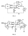
- the amplifier output signal is then referenced to ground, and this arrangement uses a so-called true ground amplifier, as shown in Figure 1 .
- the input signal to the amplifier 1 is received from a digital to analogue converter (DAC) 2.
- DAC digital to analogue converter
- the DAC is referenced to ground, and operates only in the positive voltage domain.
- the speaker 11 is connected between ground and the amplifier output.
- the DAC has a differential output of a common mode current ldaccom and a different current Idacdiff.
- the common mode current determines the voltage at one input of the amplifier, by conduction through a virtual ground resistor 3.
- the resistor is sized such that the common mode current (which is essentially constant) results in a voltage drop of 0.5Vdd.
- the difference current drives the amplifier, which has a feedback resistor 4 of the same value as the virtual earth resistor 3.
- the differential current is equal to the common mode current, so that the same 0.5Vdd voltage drop arises across the feedback resistor, and the amplifier output is zero.
- the amplifier output is centred around zero, and for this reason the amplifier requires a positive and negative voltage supply.
- US 2011/0116653 discloses an amplifier in which the output stage is split between a primary output stage and a secondary output stage. It also discloses a DC offset cancelling circuit, in which comparison of the output with true ground is used to generate an error signal, which is filtered and amplified before being subtracted from the input.
- a problem with the control of such a DC offset cancelling circuit is that different control is desirable at different times, and in a way which is not perceptible to the user when the amplifier is in use.
- an amplifier circuit comprising: a digital to analogue converter receiving a digital input and outputting an analogue output; an amplifier for amplifying the analogue output, and having a feedback impedance, wherein an output voltage from the amplifier is for connection to an output load, wherein the circuit further comprises: a voltage sensor for sensing the output voltage and generating a binary output which indicates whether the output voltage is above or below a threshold; a variable gain feedback system for generating a feedback signal from the binary output, for combination with the digital input, thereby to provide offset cancellation; and a controller for controlling the variable gain, wherein the controller is adapted to reduce the gain over time between at least two non-zero gain values to provide offset cancellation during an initial period of time of operation of the amplifier circuit.
- the amplifier can be an audio amplifier.
- the invention provides a feedback mechanism that measures the output voltage in a simple way (for example with a single comparator as analogue element) and combines (e.g. subtracts) this with the digital input. All the factors that contribute to dc-offset can be cancelled out.
- the comparator can have a threshold of 0V and thus measures if the amplifier output level is above or below ground level.
- the feedback loop adjusts the DC input signal such that the output signal is moved to 0V. This will work without the load being used (e.g. music played to a load in the form of a speaker), but it can work when using the load (e.g. playing music at the same time).
- the output can be analysed to confirm that over a long time the average signal is equally above and below zero when there is no DC component in the output signal (e.g. music).
- the digital to analogue converter can have a differential output, and the amplifier is for receiving one of the differential output signals of the digital to analogue converter to one input and the other to another input. The difference between the differential signals is thus amplified.
- the digital to analogue converter can be for converting a digital input signal into an analogue common mode current signal and an analogue differential mode current signal.
- the invention provides an adjustable loop gain which can be automated such that the speed of settling is reduced from fast to slow during start-up. Fast settling can be tolerated during start-up whereas slow settling is used during use, for example to avoid audible plop noise.
- the variable gain feedback system preferably includes a gain element and an integrator for integrating the output of the gain element.
- a circuit can then be provided for counting the integrator cycles and varying the gain at timing dependent on the counting circuit.
- the controller is adapted to change the gain at timing points when the integrator output is mid-way between minimum and maximum output levels.
- the controller can change the gain at timing points every predetermined number (e.g. 2) of crossings of the integrator output with the mid-way between minimum and maximum output levels.
- variable gain feedback system can have a fixed number of variable gain settings, such as 2,3,4 or 5.
- the primary stage is disabled during the switching on of the amplifier arrangement, and the secondary stage is turned on in graduated manner, wherein the primary stage is enabled only after the offset cancellation (i.e. after the dc offset is removed).
- the voltage sensor and variable gain feedback system is part of the secondary stage during start-up. After start-up the voltage sensor and variable gain feedback is part of the primary stage.
- the amplifier circuit can be used in a loudspeaker circuit.
- the invention also provides a method of signal amplification, comprising:
- the invention provides a true ground amplifier circuit in which a voltage sensor senses the output voltage and generates a binary output which indicates whether the output is above or below a threshold.
- a variable gain feedback system generates a feedback signal for combination with the digital input, thereby to provide offset cancellation.
- the variable gain is reduced over time to provide offset cancellation during an initial period of time of operation of the amplifier circuit. This provides offset cancellation during a start-up period, for example.
- the gain is adjusted between at least two non-zero values, which correspond to different speeds of DC offset cancellation. These different speeds can be applied at different times, depending on whether an audible effect on the output may be tolerated (for example in a mute mode) or not.
- Figure 2 shows an example of a circuit of the invention.
- the circuit comprises the DAC 2, amplifier 1, ground resistor 3, feedback resistor 4 and speaker 11 as in Figure 1 .
- the circuit comprises a comparator 5 for comparing voltage signals on opposite sides of the speaker (i.e. the amplifier output and ground) and an integrator 6.
- the comparator is thus one possible implementation of the voltage sensor, since it compares the amplifier output with ground.
- the integrator can be seen as an up/down counter.
- the integrator counter counts up as long as the amplifier output is greater than zero. It counts down as long as the amplifier output is less than zero.
- the speed of counting up/down depends on the gain of the sensor, which can be controlled by an adjustable gain element 7 with gain G.
- This invention relates in particular to the control of the gain element 7.
- the gain G will be high such that the DC-offset is cancelled in a short time, such as less than 10ms.
- Gdccan ⁇ 0 In order to keep track of slow moving effects for example due to temperature dependency it is better to take Gdccan ⁇ 0, but set it to a value low enough that it does not influence the low frequency content of the incoming music signal.
- the gain G can be calculated.
- ⁇ Uoint . fsig fs 9. ⁇ 10 - 9
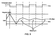
- Figure 3 shows the integrator output, based on the example of comparator signal shown.
- DCoffset_estimate Uoint ⁇ max - min 2
- the most appropriate time to reduce the gain value G is when the integrator is exactly in the middle between the maximum and minimum value, because this corresponds to the estimated DC offset value.
- a minimum and maximum detector and comparator can be used to determine the correct times to change the gain value G.
- Figure 4 shows the circuit of Figure 2 with the additional elements to control the gain value.
- a so-called zero crossing counter 8 is used to count how many times the amplifier output crosses zero based on the integrator output crossing the value max-min/2, as determined by the detector 9. The integrator output is compared with this mid level by comparator 10.
- Changing the gain G can be done after an adjustable zero crossing count. It is also possible to have more than two gain settings. Furthermore, the zero crossing counter gives information when the cancellation is completed and can be used to un-mute the amplifier.
- Figure 5 shows four gain settings G which change after every other zero crossing count.
- the change in gain setting can be seen as it causes a change in the slope of the integrator output.
- the timing is mid-way between the transition events of the comparator output.
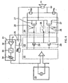
- US 2011/0116653 discloses an amplifier in which the output stage is split between a primary output stage and a secondary output stage.
- Figure 6 is taken from US 2011/0116653 .
- the signal to be amplified is connected to a primary output stage 24 and a secondary output stage 23.
- the primary stage 24 comprises a pair of transistors 27, and the secondary stage a pair of transistors 29.
- the output of primary output stage 24 is connected to speaker 11.
- a switch 25 connects the feedback loop from either the secondary stage 23 or the primary output stage 24 to the input via feedback resistor Rfbp.
- the primary output stage includes a control switch 26, which switchably connects the output from the secondary stage 23 to the midpoint node between the two primary stage transistors 27.
- the gate controls of primary stage transistors 27 are respectively under the control of further switches 28.
- the primary output stage is disabled by means of switches 28.
- the speaker can then be "soft connected", or gradually connected to the secondary stage 23 to allow a slow charging the speaker load. Provided that this charging is sufficiently slow to fall outside the audio frequency band, a plop will not be audible in the speaker.
- the switch 26 is gradually changed from a fully off state to a fully on state. The gradual change is effected by means of pulse width modulation (PWM) of the switch.
- PWM pulse width modulation
- the shape has the form of a cosine curve from 0 -180 degrees, a fast switch on (or, equivalently, switch-off) time can be realised without any audible plop.
- the primary stage can be enabled by turning on switches 28.
- Figure 6 shows a true ground configuration in which the speaker is DC coupled between the output of the primary output stage 24 and ground.
- the amplifier arrangement is balanced around ground, with a positive supply Vpos and negative supply Vneg.
- the DC offset is cancelled by means of the DC offset cancelling arrangement 31, which has the structure outlined above, of a comparator 32, integrator 33 and amplifier 34.
- the resulting signal is subtracted from the input, resulting in a reduction or removal of the DC offset.
- the primary output stage 24 is disabled.
- the secondary output stage 23 is used to remove the DC offset. Once the DC offset is removed, the primary stage is enabled by means of switches 28.
- the gain adjustment of the invention can take place during this time period to rapidly provide fast settling of the feedback loop, so that the amplifier is ready for normal operation when the primary output stage 24 is used.
- the DC offset cancellation circuit is thus associated with the secondary stage.
- the voltage sensor and variable gain feedback system is part of the secondary stage during start-up. After start-up the voltage sensor and variable gain feedback is part of the primary stage.
- the automated adjustable loop gain controlled with gain G has the advantage that the loop delay caused by signal processing, DAC, TGPHA (True Ground Headphone Amplifier) has no effect on loop stability. The delay will only result in larger excursion of the integrator and as consequence a longer period of control
- the DC offset at the output of a headphone amplifier will cause a DC current to flow that reduces play time of a mobile device.
- DC offset also is the cause of clicks and plops when switching on the headphone amplifier.
- the DC offset is caused by the input stage where mismatch in transistor and bias currents easily result in more than 1 mV DC offset at the output.
- This invention reduces the DC offset by measuring the output voltage, in a preferred example by means of a single comparator, and by using a digital control function that subtracts a value from the DAC input signal such that the average output voltage (the DC offset) becomes less than 100uV.
- the invention has been described in connection with an audio amplifier. However, it can also be used for other ac signals where low offset is needed.
Claims (15)
- Circuit amplificateur comprenant :un convertisseur numérique-analogique (2) recevant une entrée numérique et fournissant une sortie analogique ;un amplificateur (1) pour amplifier la sortie analogique, et ayant une impédance de contre-réaction (4), dans lequel une tension de sortie provenant de l'amplificateur est pour la connexion à une charge de sortie (11),ce circuit comprenant en outre :un capteur de tension (5) pour détecter la tension de sortie et pour générer une sortie binaire qui indique si la tension de sortie est au-dessus ou en dessous d'un seuil ;un système de rétroaction à gain variable (6,7,8,9,10) pour générer un signal de rétroaction depuis la sortie binaire, pour être combiné avec l'entrée numérique, de façon à fournir ainsi une annulation du décalage ; etun contrôleur pour contrôler le gain variable, ce contrôleur étant adapté de façon à réduire le gain dans le temps entre au moins deux valeurs de gain non nulles afin de fournir une annulation du décalage pendant une période initiale de temps de fonctionnement du circuit amplificateur.
- Circuit selon la revendication 1, dans lequel le convertisseur numérique-analogique (2) a une sortie différentielle, et l'amplificateur sert à recevoir un des signaux de sortie différentielle du convertisseur numérique-analogique vers une entrée et l'autre signal de sortie différentielle vers une autre entrée.
- Circuit selon la revendication 2, dans lequel le convertisseur numérique-analogique sert à convertir un signal d'entrée numérique en un signal analogique de courant de mode commun et en un signal analogique de courant de mode différentiel, le signal de courant de mode commun étant fourni à une entrée et le signal de courant de mode différentiel étant fourni à l'autre entrée de l'amplificateur.
- Circuit selon l'une quelconque des revendications précédentes, dans lequel le système de rétroaction à gain variable comprend un élément de gain (7) et un intégrateur (6) pour intégrer la sortie de l'élément de gain.
- Circuit selon la revendication 4, comprenant en outre un circuit (8, 9, 10) pour compter les cycles de l'intégrateur et pour varier le gain à une synchronisation dépendant du circuit de comptage.
- Circuit selon la revendication 4 ou 5, dans lequel le contrôleur est adapté de façon à changer le gain à des points de synchronisation lorsque la sortie de l'intégrateur est à mi-chemin entre les niveaux de sortie minimum et maximum.
- Circuit selon la revendication 6, dans lequel le contrôleur est adapté de façon à changer le gain aux points de synchronisation chaque nombre prédéterminé de croisements de la sortie de l'intégrateur avec le mi-chemin entre les niveaux de sortie minimum et maximum.
- Circuit selon la revendication 7, dans lequel le nombre prédéterminé est deux.
- Circuit selon l'une quelconque des revendications précédentes, dans lequel le capteur de tension comprend un comparateur (5).
- Circuit selon l'une quelconque des revendications précédentes, comprenant un soustracteur pour soustraire le signal de rétroaction de l'entrée numérique.
- Circuit selon l'une quelconque des revendications précédentes, dans lequel le système de rétroaction à gain variable a un nombre fixe de réglages de gain.
- Circuit selon l'une quelconque des revendications précédentes, comprenant un étage primaire (24) et un étage secondaire (23), dans lequel l'étage primaire (24) est désactivé pendant la mise en circuit du dispositif amplificateur, et l'étage secondaire (23) est mis sous tension de manière progressive, dans lequel l'étage primaire n'est activé qu'après l'annulation du décalage.
- Circuit de haut-parleur comprenant un circuit amplificateur selon l'une quelconque des revendications précédentes et un haut-parleur (11) connecté à la sortie.
- Procédé d'amplification de signal, comprenant :la conversion d'un signal d'entrée numérique en une sortie analogique ;l'amplification de la sortie analogique ;la détection de la tension de sortie analogique amplifiée et la génération d'une sortie binaire qui indique si la tension de sortie analogique amplifiée est au-dessus ou en dessous d'un seuil ;la génération d'un signal de rétroaction depuis la sortie binaire, pour être combiné avec l'entrée numérique, afin de fournir ainsi une annulation du décalage ; etle contrôle d'un gain variable du signal de rétroaction entre au moins deux valeurs de gain non nulles en réduisant le gain dans le temps pour fournir une annulation du décalage pendant une période initiale de temps de fonctionnement du circuit amplificateur.
- Procédé d'utilisation d'un amplificateur comprenant un étage primaire (24) et un étage secondaire (23), ce procédé comprenant :la désactivation de l'étage primaire de l'amplificateur pendant la mise en circuit de l'amplificateur ;la mise sous tension de l'étage secondaire de l'amplificateur d'une manière progressive en utilisant le procédé de la revendication 14 ; etl'activation de l'étage primaire après l'annulation du décalage.
Priority Applications (3)
| Application Number | Priority Date | Filing Date | Title |
|---|---|---|---|
| EP13167118.2A EP2802074B1 (fr) | 2013-05-08 | 2013-05-08 | Circuit amplificateur et procédé d'amplification |
| CN201410128328.1A CN104143984B (zh) | 2013-05-08 | 2014-04-01 | 放大器电路及其放大方法 |
| US14/258,687 US9154098B2 (en) | 2013-05-08 | 2014-04-22 | Amplifier circuit and amplification method |
Applications Claiming Priority (1)
| Application Number | Priority Date | Filing Date | Title |
|---|---|---|---|
| EP13167118.2A EP2802074B1 (fr) | 2013-05-08 | 2013-05-08 | Circuit amplificateur et procédé d'amplification |
Publications (2)
| Publication Number | Publication Date |
|---|---|
| EP2802074A1 EP2802074A1 (fr) | 2014-11-12 |
| EP2802074B1 true EP2802074B1 (fr) | 2015-08-05 |
Family
ID=48236795
Family Applications (1)
| Application Number | Title | Priority Date | Filing Date |
|---|---|---|---|
| EP13167118.2A Active EP2802074B1 (fr) | 2013-05-08 | 2013-05-08 | Circuit amplificateur et procédé d'amplification |
Country Status (3)
| Country | Link |
|---|---|
| US (1) | US9154098B2 (fr) |
| EP (1) | EP2802074B1 (fr) |
| CN (1) | CN104143984B (fr) |
Families Citing this family (7)
| Publication number | Priority date | Publication date | Assignee | Title |
|---|---|---|---|---|
| EP3145216B1 (fr) * | 2015-09-17 | 2018-11-14 | Nxp B.V. | Système amplificateur |
| EP3229371B1 (fr) * | 2016-04-06 | 2020-03-11 | Nxp B.V. | Système d'amplificateur audio |
| US10164576B2 (en) * | 2017-04-28 | 2018-12-25 | Cirrus Logic, Inc. | Amplifier offset cancellation using amplifier supply voltage |
| CN110603732B (zh) | 2018-04-12 | 2023-05-26 | 深圳市汇顶科技股份有限公司 | 运算放大器及其控制方法 |
| TWI703817B (zh) * | 2019-09-02 | 2020-09-01 | 瑞昱半導體股份有限公司 | 音訊裝置、具有音訊裝置的電子裝置及其音訊處理方法 |
| TWI748261B (zh) * | 2019-10-15 | 2021-12-01 | 瑞昱半導體股份有限公司 | 回授系統與相關的訊號處理方法 |
| US11228289B1 (en) | 2020-08-24 | 2022-01-18 | Cirrus Logic, Inc. | Amplifiers |
Family Cites Families (15)
| Publication number | Priority date | Publication date | Assignee | Title |
|---|---|---|---|---|
| FR2473810A1 (fr) * | 1980-01-09 | 1981-07-17 | Ibm France | Procede de compensation de la tension de decalage d'un amplificateur differentiel et macro-fonctionnelle en resultant |
| US6426663B1 (en) * | 1996-03-04 | 2002-07-30 | Delphi Technologies, Inc. | Analog/digital feedback circuitry for minimizing DC offset variations in an analog signal |
| US6114980A (en) * | 1999-04-13 | 2000-09-05 | Motorola, Inc. | Method and apparatus for settling a DC offset |
| US6317064B1 (en) * | 2000-02-29 | 2001-11-13 | Motorola, Inc. | DC offset correction adaptable to multiple requirements |
| JP3984482B2 (ja) * | 2002-02-04 | 2007-10-03 | 富士通株式会社 | Dcオフセットキャンセル回路 |
| US7254244B2 (en) * | 2003-07-28 | 2007-08-07 | Sigmatel, Inc. | Pop and click reduction using DAC power up and power down processing |
| KR100564606B1 (ko) * | 2004-01-29 | 2006-03-28 | 삼성전자주식회사 | 연산 증폭기의 오프셋 제거 장치 |
| US20100278355A1 (en) * | 2009-04-29 | 2010-11-04 | Yamkovoy Paul G | Feedforward-Based ANR Adjustment Responsive to Environmental Noise Levels |
| FR2946201A1 (fr) * | 2009-05-29 | 2010-12-03 | St Ericsson Grenoble Sas | Annulation d'offset pour amplificateur audio |
| US8737636B2 (en) * | 2009-07-10 | 2014-05-27 | Qualcomm Incorporated | Systems, methods, apparatus, and computer-readable media for adaptive active noise cancellation |
| US8264268B2 (en) * | 2009-07-27 | 2012-09-11 | Electronics And Telecommunications Research Institute | Offset-voltage calibration circuit |
| EP2323254B1 (fr) | 2009-11-16 | 2012-06-06 | Nxp B.V. | Amplificateur sans plop |
| US20120041695A1 (en) * | 2010-08-16 | 2012-02-16 | Csi Technology, Inc. | Integrated vibration measurement and analysis system |
| US8482347B2 (en) * | 2010-12-13 | 2013-07-09 | Broadcom Corporation | Amplifier with reduced on/off transient and multi-point offset compensation |
| GB2485620B (en) * | 2010-12-16 | 2013-04-17 | Wolfson Microelectronics Plc | DC offset compensation |
-
2013
- 2013-05-08 EP EP13167118.2A patent/EP2802074B1/fr active Active
-
2014
- 2014-04-01 CN CN201410128328.1A patent/CN104143984B/zh active Active
- 2014-04-22 US US14/258,687 patent/US9154098B2/en active Active
Also Published As
| Publication number | Publication date |
|---|---|
| EP2802074A1 (fr) | 2014-11-12 |
| US20140340147A1 (en) | 2014-11-20 |
| CN104143984A (zh) | 2014-11-12 |
| CN104143984B (zh) | 2017-09-08 |
| US9154098B2 (en) | 2015-10-06 |
Similar Documents
| Publication | Publication Date | Title |
|---|---|---|
| EP2802074B1 (fr) | Circuit amplificateur et procédé d'amplification | |
| US11431310B2 (en) | Tracking and correcting gain of open-loop driver in a multi-path processing system | |
| US7312654B2 (en) | Quiet power up and power down of a digital audio amplifier | |
| US9065401B2 (en) | Amplification systems and methods with noise reductions | |
| US8040184B2 (en) | Class-D amplifier | |
| US9019012B2 (en) | Amplifier circuit with offset control | |
| US20070058711A1 (en) | Recovery from clipping events in a class d amplifier | |
| US8289075B2 (en) | Class-D amplifier | |
| CN107005207B (zh) | 具有可调节斜升/斜降增益以最小化或消除气爆噪声的放大器 | |
| EP2127070B1 (fr) | Système de traitement de données pour correction d'écrêtage | |
| US10483924B2 (en) | Systems and methods for predictive switching in audio amplifiers | |
| US10404248B2 (en) | Calibration of a dual-path pulse width modulation system | |
| CN110582935A (zh) | 在具有多个回放路径的音频系统中进行切换 | |
| US10476455B1 (en) | Apparatus and method of suppressing transient noise during transition for class-D amplifier system having one or more pulse width modulator output paths | |
| JPH11163650A (ja) | 可変要素として電圧制御抵抗器を備えた線形リミタ回路を使用した自動ゲイン制御方法及び装置 | |
| EP0427135A2 (fr) | Circuit pour mesurer la distorsion de sortie, en particulier d'étages de sortie de dispositifs audio | |
| WO2019077889A1 (fr) | Circuit et procédé d'élimination de bruit ainsi que dispositif de commande de moteur | |
| JP5343782B2 (ja) | D級増幅器 | |
| JP3638442B2 (ja) | ボリウム回路 | |
| US8928390B2 (en) | Method to improve response speed of RMS detectors | |
| JPH03175709A (ja) | 高周波増幅器の電力制御回路 | |
| JP2574706B2 (ja) | 送信機 |
Legal Events
| Date | Code | Title | Description |
|---|---|---|---|
| PUAI | Public reference made under article 153(3) epc to a published international application that has entered the european phase |
Free format text: ORIGINAL CODE: 0009012 |
|
| 17P | Request for examination filed |
Effective date: 20140326 |
|
| AK | Designated contracting states |
Kind code of ref document: A1 Designated state(s): AL AT BE BG CH CY CZ DE DK EE ES FI FR GB GR HR HU IE IS IT LI LT LU LV MC MK MT NL NO PL PT RO RS SE SI SK SM TR |
|
| AX | Request for extension of the european patent |
Extension state: BA ME |
|
| GRAP | Despatch of communication of intention to grant a patent |
Free format text: ORIGINAL CODE: EPIDOSNIGR1 |
|
| INTG | Intention to grant announced |
Effective date: 20141216 |
|
| RIN1 | Information on inventor provided before grant (corrected) |
Inventor name: SCHUURMANS, HAN Inventor name: VAN DOMMELEN, MAARTEN |
|
| GRAP | Despatch of communication of intention to grant a patent |
Free format text: ORIGINAL CODE: EPIDOSNIGR1 |
|
| INTG | Intention to grant announced |
Effective date: 20150430 |
|
| RBV | Designated contracting states (corrected) |
Designated state(s): AL AT BE BG CH CY CZ DE DK EE ES FI FR GB GR HR HU IE IS IT LI LT LU LV MC MK MT NL NO PL PT RO RS SE SI SK SM TR |
|
| GRAS | Grant fee paid |
Free format text: ORIGINAL CODE: EPIDOSNIGR3 |
|
| GRAA | (expected) grant |
Free format text: ORIGINAL CODE: 0009210 |
|
| AK | Designated contracting states |
Kind code of ref document: B1 Designated state(s): AL AT BE BG CH CY CZ DE DK EE ES FI FR GB GR HR HU IE IS IT LI LT LU LV MC MK MT NL NO PL PT RO RS SE SI SK SM TR |
|
| REG | Reference to a national code |
Ref country code: GB Ref legal event code: FG4D |
|
| REG | Reference to a national code |
Ref country code: CH Ref legal event code: EP |
|
| REG | Reference to a national code |
Ref country code: AT Ref legal event code: REF Ref document number: 741192 Country of ref document: AT Kind code of ref document: T Effective date: 20150815 |
|
| REG | Reference to a national code |
Ref country code: IE Ref legal event code: FG4D |
|
| REG | Reference to a national code |
Ref country code: DE Ref legal event code: R096 Ref document number: 602013002486 Country of ref document: DE |
|
| REG | Reference to a national code |
Ref country code: AT Ref legal event code: MK05 Ref document number: 741192 Country of ref document: AT Kind code of ref document: T Effective date: 20150805 |
|
| REG | Reference to a national code |
Ref country code: LT Ref legal event code: MG4D |
|
| REG | Reference to a national code |
Ref country code: NL Ref legal event code: MP Effective date: 20150805 |
|
| PG25 | Lapsed in a contracting state [announced via postgrant information from national office to epo] |
Ref country code: NO Free format text: LAPSE BECAUSE OF FAILURE TO SUBMIT A TRANSLATION OF THE DESCRIPTION OR TO PAY THE FEE WITHIN THE PRESCRIBED TIME-LIMIT Effective date: 20151105 Ref country code: GR Free format text: LAPSE BECAUSE OF FAILURE TO SUBMIT A TRANSLATION OF THE DESCRIPTION OR TO PAY THE FEE WITHIN THE PRESCRIBED TIME-LIMIT Effective date: 20151106 Ref country code: FI Free format text: LAPSE BECAUSE OF FAILURE TO SUBMIT A TRANSLATION OF THE DESCRIPTION OR TO PAY THE FEE WITHIN THE PRESCRIBED TIME-LIMIT Effective date: 20150805 Ref country code: LT Free format text: LAPSE BECAUSE OF FAILURE TO SUBMIT A TRANSLATION OF THE DESCRIPTION OR TO PAY THE FEE WITHIN THE PRESCRIBED TIME-LIMIT Effective date: 20150805 Ref country code: LV Free format text: LAPSE BECAUSE OF FAILURE TO SUBMIT A TRANSLATION OF THE DESCRIPTION OR TO PAY THE FEE WITHIN THE PRESCRIBED TIME-LIMIT Effective date: 20150805 |
|
| PG25 | Lapsed in a contracting state [announced via postgrant information from national office to epo] |
Ref country code: SE Free format text: LAPSE BECAUSE OF FAILURE TO SUBMIT A TRANSLATION OF THE DESCRIPTION OR TO PAY THE FEE WITHIN THE PRESCRIBED TIME-LIMIT Effective date: 20150805 Ref country code: AT Free format text: LAPSE BECAUSE OF FAILURE TO SUBMIT A TRANSLATION OF THE DESCRIPTION OR TO PAY THE FEE WITHIN THE PRESCRIBED TIME-LIMIT Effective date: 20150805 Ref country code: ES Free format text: LAPSE BECAUSE OF FAILURE TO SUBMIT A TRANSLATION OF THE DESCRIPTION OR TO PAY THE FEE WITHIN THE PRESCRIBED TIME-LIMIT Effective date: 20150805 Ref country code: RS Free format text: LAPSE BECAUSE OF FAILURE TO SUBMIT A TRANSLATION OF THE DESCRIPTION OR TO PAY THE FEE WITHIN THE PRESCRIBED TIME-LIMIT Effective date: 20150805 Ref country code: IS Free format text: LAPSE BECAUSE OF FAILURE TO SUBMIT A TRANSLATION OF THE DESCRIPTION OR TO PAY THE FEE WITHIN THE PRESCRIBED TIME-LIMIT Effective date: 20151205 Ref country code: HR Free format text: LAPSE BECAUSE OF FAILURE TO SUBMIT A TRANSLATION OF THE DESCRIPTION OR TO PAY THE FEE WITHIN THE PRESCRIBED TIME-LIMIT Effective date: 20150805 Ref country code: PL Free format text: LAPSE BECAUSE OF FAILURE TO SUBMIT A TRANSLATION OF THE DESCRIPTION OR TO PAY THE FEE WITHIN THE PRESCRIBED TIME-LIMIT Effective date: 20150805 Ref country code: PT Free format text: LAPSE BECAUSE OF FAILURE TO SUBMIT A TRANSLATION OF THE DESCRIPTION OR TO PAY THE FEE WITHIN THE PRESCRIBED TIME-LIMIT Effective date: 20151207 |
|
| PG25 | Lapsed in a contracting state [announced via postgrant information from national office to epo] |
Ref country code: NL Free format text: LAPSE BECAUSE OF FAILURE TO SUBMIT A TRANSLATION OF THE DESCRIPTION OR TO PAY THE FEE WITHIN THE PRESCRIBED TIME-LIMIT Effective date: 20150805 |
|
| REG | Reference to a national code |
Ref country code: FR Ref legal event code: PLFP Year of fee payment: 4 |
|
| PG25 | Lapsed in a contracting state [announced via postgrant information from national office to epo] |
Ref country code: CZ Free format text: LAPSE BECAUSE OF FAILURE TO SUBMIT A TRANSLATION OF THE DESCRIPTION OR TO PAY THE FEE WITHIN THE PRESCRIBED TIME-LIMIT Effective date: 20150805 Ref country code: IT Free format text: LAPSE BECAUSE OF FAILURE TO SUBMIT A TRANSLATION OF THE DESCRIPTION OR TO PAY THE FEE WITHIN THE PRESCRIBED TIME-LIMIT Effective date: 20150805 Ref country code: EE Free format text: LAPSE BECAUSE OF FAILURE TO SUBMIT A TRANSLATION OF THE DESCRIPTION OR TO PAY THE FEE WITHIN THE PRESCRIBED TIME-LIMIT Effective date: 20150805 Ref country code: DK Free format text: LAPSE BECAUSE OF FAILURE TO SUBMIT A TRANSLATION OF THE DESCRIPTION OR TO PAY THE FEE WITHIN THE PRESCRIBED TIME-LIMIT Effective date: 20150805 Ref country code: SK Free format text: LAPSE BECAUSE OF FAILURE TO SUBMIT A TRANSLATION OF THE DESCRIPTION OR TO PAY THE FEE WITHIN THE PRESCRIBED TIME-LIMIT Effective date: 20150805 |
|
| REG | Reference to a national code |
Ref country code: DE Ref legal event code: R097 Ref document number: 602013002486 Country of ref document: DE |
|
| PG25 | Lapsed in a contracting state [announced via postgrant information from national office to epo] |
Ref country code: RO Free format text: LAPSE BECAUSE OF FAILURE TO SUBMIT A TRANSLATION OF THE DESCRIPTION OR TO PAY THE FEE WITHIN THE PRESCRIBED TIME-LIMIT Effective date: 20150805 |
|
| PLBE | No opposition filed within time limit |
Free format text: ORIGINAL CODE: 0009261 |
|
| STAA | Information on the status of an ep patent application or granted ep patent |
Free format text: STATUS: NO OPPOSITION FILED WITHIN TIME LIMIT |
|
| 26N | No opposition filed |
Effective date: 20160509 |
|
| PG25 | Lapsed in a contracting state [announced via postgrant information from national office to epo] |
Ref country code: SI Free format text: LAPSE BECAUSE OF FAILURE TO SUBMIT A TRANSLATION OF THE DESCRIPTION OR TO PAY THE FEE WITHIN THE PRESCRIBED TIME-LIMIT Effective date: 20150805 Ref country code: BE Free format text: LAPSE BECAUSE OF NON-PAYMENT OF DUE FEES Effective date: 20160531 |
|
| PG25 | Lapsed in a contracting state [announced via postgrant information from national office to epo] |
Ref country code: BE Free format text: LAPSE BECAUSE OF FAILURE TO SUBMIT A TRANSLATION OF THE DESCRIPTION OR TO PAY THE FEE WITHIN THE PRESCRIBED TIME-LIMIT Effective date: 20150805 Ref country code: LU Free format text: LAPSE BECAUSE OF FAILURE TO SUBMIT A TRANSLATION OF THE DESCRIPTION OR TO PAY THE FEE WITHIN THE PRESCRIBED TIME-LIMIT Effective date: 20160508 |
|
| REG | Reference to a national code |
Ref country code: CH Ref legal event code: PL |
|
| PG25 | Lapsed in a contracting state [announced via postgrant information from national office to epo] |
Ref country code: CH Free format text: LAPSE BECAUSE OF NON-PAYMENT OF DUE FEES Effective date: 20160531 Ref country code: LI Free format text: LAPSE BECAUSE OF NON-PAYMENT OF DUE FEES Effective date: 20160531 |
|
| REG | Reference to a national code |
Ref country code: IE Ref legal event code: MM4A |
|
| REG | Reference to a national code |
Ref country code: FR Ref legal event code: PLFP Year of fee payment: 5 |
|
| PG25 | Lapsed in a contracting state [announced via postgrant information from national office to epo] |
Ref country code: IE Free format text: LAPSE BECAUSE OF NON-PAYMENT OF DUE FEES Effective date: 20160508 |
|
| REG | Reference to a national code |
Ref country code: FR Ref legal event code: PLFP Year of fee payment: 6 |
|
| PG25 | Lapsed in a contracting state [announced via postgrant information from national office to epo] |
Ref country code: HU Free format text: LAPSE BECAUSE OF FAILURE TO SUBMIT A TRANSLATION OF THE DESCRIPTION OR TO PAY THE FEE WITHIN THE PRESCRIBED TIME-LIMIT; INVALID AB INITIO Effective date: 20130508 Ref country code: SM Free format text: LAPSE BECAUSE OF FAILURE TO SUBMIT A TRANSLATION OF THE DESCRIPTION OR TO PAY THE FEE WITHIN THE PRESCRIBED TIME-LIMIT Effective date: 20150805 |
|
| PG25 | Lapsed in a contracting state [announced via postgrant information from national office to epo] |
Ref country code: CY Free format text: LAPSE BECAUSE OF FAILURE TO SUBMIT A TRANSLATION OF THE DESCRIPTION OR TO PAY THE FEE WITHIN THE PRESCRIBED TIME-LIMIT Effective date: 20150805 Ref country code: MT Free format text: LAPSE BECAUSE OF NON-PAYMENT OF DUE FEES Effective date: 20160531 Ref country code: MK Free format text: LAPSE BECAUSE OF FAILURE TO SUBMIT A TRANSLATION OF THE DESCRIPTION OR TO PAY THE FEE WITHIN THE PRESCRIBED TIME-LIMIT Effective date: 20150805 Ref country code: MC Free format text: LAPSE BECAUSE OF FAILURE TO SUBMIT A TRANSLATION OF THE DESCRIPTION OR TO PAY THE FEE WITHIN THE PRESCRIBED TIME-LIMIT Effective date: 20150805 |
|
| PG25 | Lapsed in a contracting state [announced via postgrant information from national office to epo] |
Ref country code: BG Free format text: LAPSE BECAUSE OF FAILURE TO SUBMIT A TRANSLATION OF THE DESCRIPTION OR TO PAY THE FEE WITHIN THE PRESCRIBED TIME-LIMIT Effective date: 20150805 |
|
| PG25 | Lapsed in a contracting state [announced via postgrant information from national office to epo] |
Ref country code: TR Free format text: LAPSE BECAUSE OF FAILURE TO SUBMIT A TRANSLATION OF THE DESCRIPTION OR TO PAY THE FEE WITHIN THE PRESCRIBED TIME-LIMIT Effective date: 20150805 Ref country code: AL Free format text: LAPSE BECAUSE OF FAILURE TO SUBMIT A TRANSLATION OF THE DESCRIPTION OR TO PAY THE FEE WITHIN THE PRESCRIBED TIME-LIMIT Effective date: 20150805 |
|
| REG | Reference to a national code |
Ref country code: DE Ref legal event code: R081 Ref document number: 602013002486 Country of ref document: DE Owner name: GOODIX TECHNOLOGY (HK) COMPANY LIMITED, CN Free format text: FORMER OWNER: NXP B.V., EINDHOVEN, NL |
|
| REG | Reference to a national code |
Ref country code: GB Ref legal event code: 732E Free format text: REGISTERED BETWEEN 20200917 AND 20200923 |
|
| PGFP | Annual fee paid to national office [announced via postgrant information from national office to epo] |
Ref country code: FR Payment date: 20230526 Year of fee payment: 11 Ref country code: DE Payment date: 20230519 Year of fee payment: 11 |
|
| PGFP | Annual fee paid to national office [announced via postgrant information from national office to epo] |
Ref country code: GB Payment date: 20230524 Year of fee payment: 11 |