EP2802003B1 - Verfahren zur Bereitstellung einer Gate-Metallschicht einer Transistorvorrichtung - Google Patents
Verfahren zur Bereitstellung einer Gate-Metallschicht einer Transistorvorrichtung Download PDFInfo
- Publication number
- EP2802003B1 EP2802003B1 EP13166902.0A EP13166902A EP2802003B1 EP 2802003 B1 EP2802003 B1 EP 2802003B1 EP 13166902 A EP13166902 A EP 13166902A EP 2802003 B1 EP2802003 B1 EP 2802003B1
- Authority
- EP
- European Patent Office
- Prior art keywords
- layer
- metal
- diffusion layer
- spacers
- gate
- Prior art date
- Legal status (The legal status is an assumption and is not a legal conclusion. Google has not performed a legal analysis and makes no representation as to the accuracy of the status listed.)
- Active
Links
Images

Classifications
-
- H—ELECTRICITY
- H01—ELECTRIC ELEMENTS
- H01L—SEMICONDUCTOR DEVICES NOT COVERED BY CLASS H10
- H01L21/00—Processes or apparatus adapted for the manufacture or treatment of semiconductor or solid state devices or of parts thereof
- H01L21/02—Manufacture or treatment of semiconductor devices or of parts thereof
- H01L21/04—Manufacture or treatment of semiconductor devices or of parts thereof the devices having potential barriers, e.g. a PN junction, depletion layer or carrier concentration layer
- H01L21/18—Manufacture or treatment of semiconductor devices or of parts thereof the devices having potential barriers, e.g. a PN junction, depletion layer or carrier concentration layer the devices having semiconductor bodies comprising elements of Group IV of the Periodic Table or AIIIBV compounds with or without impurities, e.g. doping materials
- H01L21/28—Manufacture of electrodes on semiconductor bodies using processes or apparatus not provided for in groups H01L21/20 - H01L21/268
- H01L21/28008—Making conductor-insulator-semiconductor electrodes
- H01L21/28017—Making conductor-insulator-semiconductor electrodes the insulator being formed after the semiconductor body, the semiconductor being silicon
- H01L21/28026—Making conductor-insulator-semiconductor electrodes the insulator being formed after the semiconductor body, the semiconductor being silicon characterised by the conductor
- H01L21/28097—Making conductor-insulator-semiconductor electrodes the insulator being formed after the semiconductor body, the semiconductor being silicon characterised by the conductor the final conductor layer next to the insulator being a metallic silicide
-
- H—ELECTRICITY
- H10—SEMICONDUCTOR DEVICES; ELECTRIC SOLID-STATE DEVICES NOT OTHERWISE PROVIDED FOR
- H10D—INORGANIC ELECTRIC SEMICONDUCTOR DEVICES
- H10D64/00—Electrodes of devices having potential barriers
- H10D64/01—Manufacture or treatment
- H10D64/017—Manufacture or treatment using dummy gates in processes wherein at least parts of the final gates are self-aligned to the dummy gates, i.e. replacement gate processes
-
- H—ELECTRICITY
- H10—SEMICONDUCTOR DEVICES; ELECTRIC SOLID-STATE DEVICES NOT OTHERWISE PROVIDED FOR
- H10D—INORGANIC ELECTRIC SEMICONDUCTOR DEVICES
- H10D64/00—Electrodes of devices having potential barriers
- H10D64/60—Electrodes characterised by their materials
- H10D64/66—Electrodes having a conductor capacitively coupled to a semiconductor by an insulator, e.g. MIS electrodes
- H10D64/667—Electrodes having a conductor capacitively coupled to a semiconductor by an insulator, e.g. MIS electrodes the conductor comprising a layer of alloy material, compound material or organic material contacting the insulator, e.g. TiN workfunction layers
- H10D64/668—Electrodes having a conductor capacitively coupled to a semiconductor by an insulator, e.g. MIS electrodes the conductor comprising a layer of alloy material, compound material or organic material contacting the insulator, e.g. TiN workfunction layers the layer being a silicide, e.g. TiSi2
-
- H—ELECTRICITY
- H10—SEMICONDUCTOR DEVICES; ELECTRIC SOLID-STATE DEVICES NOT OTHERWISE PROVIDED FOR
- H10D—INORGANIC ELECTRIC SEMICONDUCTOR DEVICES
- H10D30/00—Field-effect transistors [FET]
- H10D30/60—Insulated-gate field-effect transistors [IGFET]
Definitions
- the present disclosure relates to a method for providing a gate metal layer in a transistor device. More specifically it related to a method for providing a gate metal layer in a transistor device having relatively small gate dimensions, e.g. relatively small gate width.
- a process of manufacturing a MOS semiconductor transistor can be based on a so called gate-last approach.
- a gate-last approach also referred to as replacement-gate (RMG) approach
- the metal gate deposition occurs after a number of activation anneal steps (i.e. junction activation, source/drain activation) and a silicidation step.
- a gate-first approach the metal gate is deposited on a high-k gate dielectric prior to the activation anneal steps, such that the metal gate is exposed to high temperatures (temperatures up to 1100 degrees Celsius or higher), which can be detrimental for the proper working of the device. In the gate-last approach, the metal of the metal gate is thus not exposed to these high temperatures.
- a gate dielectric layer and a dummy gate electrode layer are provided and patterned on a substrate, thereby forming a dummy gate stack. Later, spacers are provided aside the dummy gate stack, and activation of the source/drain areas is performed. An additional silicidation process can be performed, which is known to the skilled person. The patterned dummy gate stack is then completely or partially removed and replaced by a final gate stack.
- CMOS Complementary MOS
- NMOS n-channel and p-channel transistors.
- the threshold voltage Vt is influenced by what is called the effective work function difference ( ⁇ WF eff ).
- effective work function differences of the respective PMOS and NMOS gate materials (gate stacks) and their corresponding channel regions are typically independently established through channel processing and gate processing.
- gate dielectric consisting i.e. of a host dielectric and possible different capping layers
- gate electrode Consisting i.e.
- the gate processing itself i.e. the sequence of the different processes and/or the thermal treatments applied
- the gate processing itself may have an influence on the effective work function of the gate stack (device) (WF eff ).
- TiAl is known to be an appropriate metal for controlling the threshold voltage.
- the TiAl metal is generally formed by Physical Vapor Deposition (PVD) or Chemical Vapor Deposition (CVD). It is though difficult if not impossible to provide the final gate stack for small gate widths (e.g. filling the gap between the spacers generated by the dummy gate structure), biasing a good control of the Vt.
- a process for producing an electronic component including covering a substrate with a portion defining, with the substrate, a volume at least partly filled with a temporary material.
- the temporary material is then removed via chimney for access to said volume.
- a deposition of a fill material is then made in said volume, the fill material being obtained from precursors supplied via the chimney.
- a method for manufacturing a field effect transistor comprising the steps of:
- the portion of the front surface can correspond to an upper surface of the set of spacers.
- the upper surface of the set of spacers and the front surface of the one or more embedding layers may lie in a single plane. This single plane may have been defined by a planarization process, as for instance a CMP process, performed on an intermediate structure comprising a dummy gate structure and one or more transistor embedding layers surrounding the dummy gate structure.
- the diffusion layer is continuous. It is preferably a conformal layer which follows substantially the surface of the underlying topology, and has a uniform thickness. Such a conformal layer does not substantially change the underlying topology, i.e. the shape of the underlying surface.
- the diffusion layer comprises silicon. It may comprise for instance polycrystalline silicon, multicrystalline silicon or monocrystalline silicon.
- the diffusion layer has a thickness within the range of 2 to 10 nm.
- the metal layer comprises Aluminum, Indium, Gallium or Nickel.
- the anneal step is performed at a temperature in between 400°C and 600°C.
- the anneal step has a duration of 1 to 10 minutes.
- the vertical distance between the metal layer in an area corresponding to the upper surface of the set of spacers and the upper surface of the diffusion layer in an area on top of the gate dielectric layer is smaller than 170nm. This is advantageous as it reduces the time period for successfully driving diffusion of the metal into the diffusion layer, and for further diffusing the metal in the diffusion layer towards the portion of the diffusion layer in the area corresponding to the area of the gate dielectric.
- the vertical distance between the metal layer in an area corresponding to the upper surface of the set of spacers and the upper surface of the diffusion layer in an area on top of the gate dielectric layer is larger than 60nm. It will be appreciated to the skilled person that methods according to aspects of the present invention can be applied for a relatively large vertical distance between the metal layer in an area corresponding to the upper surface of the set of spacers and the upper surface of the diffusion layer in an area on top of the gate dielectric layer.
- the diffusion layer is deposited by means of Chemical Vapor Deposition (CVD).
- CVD Chemical Vapor Deposition
- the anneal step is such that the diffusion layer and the metal layer merge completely into a single merged layer of mixed constitution, in other words into a single merged layer which is homogeneous, i.e. with constant constitution.
- the method further comprises performing a Chemical Mechanical Polishing (CMP) step after applying the anneal step and filling the area in between the inner sidewalls of the set of spacers with a final gate metal filling layer.
- CMP Chemical Mechanical Polishing
- the field effect transistor is of the non-planar type comprising at least one FIN structure protruding from a front surface of the substrate, and wherein the dummy gate structure is provided at least partially on the FIN structure and at least partially adjacent to the FIN structure.
- the gate electrode layer has a thickness between 5 to 20 nm.
- the gate electrode layer comprises SiAl, Siln, SiGa or SiNi.
- FIGS. 1 to 6 illustrate a preferred embodiment of the present disclosure.
- top, bottom, over, under and the like in the description and the claims are used for descriptive purposes and not necessarily for describing relative positions. The terms so used are interchangeable under appropriate circumstances and the embodiments of the disclosure described herein can operate in other orientations than described or illustrated herein.
- the "substrate” may include a semiconductor substrate such as e.g. a silicon, a gallium arsenide (GaAs), a gallium arsenide phosphide (GaAsP), an indium phosphide (InP), a germanium (Ge), or a silicon germanium (SiGe) substrate.
- the "substrate” may include for example, an insulating layer such as a SiO 2 or a Si 3 N 4 layer in addition to a semiconductor substrate portion.
- substrate also includes silicon-on-glass, silicon-on-sapphire substrates.
- substrate is thus used to define generally the elements for layers that underlie a layer or portions of interest.
- the "substrate” may be any other base on which a layer is formed, for example a glass or metal layer. Accordingly a substrate may be a wafer such as a blanket wafer or may be a layer applied to another base material, e.g. an epitaxial layer grown onto a lower layer.
- FIG.1 illustrates a semiconductor substrate 1, e.g. a silicon substrate.
- the substrate may comprise multiple distinct regions. Most preferably two distinct regions may be defined in the substrate 1, a first region and a second region.
- the first region may also be referred as the first active region of the device (NMOS or PMOS region) and the second region may also be referred as the second active region of the device (PMOS or NMOS region respectively).
- the first region and the second region may be electrically isolated from each other by an insulating region.
- a possible way to isolate the first and second region from each other is by using shallow trench isolation (STI) in between.
- STI shallow trench isolation
- STI is typically a deep narrow trench, filled with oxide, etched into the semiconductor substrate in between adjacent devices in an integrated circuit to provide electrical isolation between.
- LOC local oxidation of silicon
- the dielectric layer 2 may be a layer of insulating material, such as for example silicon dioxide (SiO 2 ), silicon nitride (SiN) or silicon oxynitride (Si x O y N 1-x-y ) or more preferably any high-k dielectric material (i.e. k > 3.9) such as for example HfO 2 , TaO x , Al 2 O y , or any combination made thereof.
- the gate dielectric layer may be formed by thermal oxidation, atomic layer deposition (ALD) or chemical vapor deposition (CVD) or physical vapor deposition (PVD), or any other suitable method known to a person skilled in the art.
- the gate dielectric layer may comprise a stack of dielectric materials, such as for example a high-k material (e.g. HfO 2 ) formed on top of an (optional) interfacial dielectric layer (e.g. SiO 2 - not shown) between the substrate 1 and high-k material.
- a high-k material e.g. HfO 2
- an interfacial dielectric layer e.g. SiO 2 - not shown
- a dummy gate electrode layer is provided on the gate dielectric layer 2. Spacers are formed.
- the patterned dummy gate electrode layer is removed, resulting in a device depicted in Fig. 1 .
- the removal of the patterned dummy gate electrode may be done for example by means of a wet etch process or other etch processes known by the skilled person.
- FIG. 1 which is of the planar type, i.e. process steps comprising patterning (e.g. using conventional lithography) the gate dielectric layer 2 and the dummy gate electrode layer to form a dummy gate stack, providing one or more spacers 3 (31,32) aside of the dummy gate stack, activation of the source (S) /drain (D) regions (extension regions/junction regions) in the first region and additional silicidation.
- S source
- D extension regions/junction regions
- annealing process comprises a high temperature process.
- the temperature of the annealing process is typically higher than 500 degrees Celsius, preferably higher than 800 degrees Celsius, more preferably in the range of 800 degrees Celsius to 1200 degrees Celsius.
- Spike annealing or rapid thermal annealing (RTA) may be used.
- the spacers 3 (31,32) preferably comprise an insulating material such as for example silicon dioxide (SiO 2 ), silicon nitride (SiN) or silicon oxynitride (SiON). They can for instance comprise a stack structure as a for instance SiN/SiO. Spacers 3 (31,32) may be deposited by ALD or CVD and patterned by anisotropic etching, or any other suitable method known to a person skilled in the art.
- the underlying gate dielectric layer 2 is exposed.
- the removal of the dummy gate electrode material may be done using an etching process which is selective towards the underlying gate dielectric material.
- first one or more embedding layers 8, for instance a dielectric layer 8 may be formed.
- the formation of the dielectric layer 8 (e.g. premetal dielectric layer) may be done for example by depositing the dielectric layer 8 using CVD, followed by polishing back to a level corresponding to a front surface 81, 321, 311 (e.g. using CMP) of the dielectric layer 8 (or embedding layer or stack of embedding layers; or stack of dielectric embedding layers) to expose the dummy gate electrode material in the gate region.
- the dielectric layer 8 forms a protective layer for protecting the underlying source/drain regions and silicide regions and spacers 3 during the subsequent etching process for removing the dummy gate electrode material.
- a protective dielectric liner may be formed on the source/drain regions and silicide regions and aside of the spacers 3.
- the dummy gate electrode material may be removed. After removing the dummy gate electrode material a trench is formed (having a depth d) in the area in between the sidewall spacers 3, delimited by the upper surface of the gate dielectric 2 and the inner sidewalls of the spacer structure 3 (322). After removal of the dummy gate electrode material, the gate dielectric layer 2 is still present in the gate stack.
- a final gate electrode layer is then applied in between said inner sidewalls of the set of spacers. According to preferred embodiments of the present invention, this can be achieved as follows.
- a connected, conformal diffusion layer 4 is applied, for instance a silicon layer, the diffusion layer extending at least on top of the gate dielectric layer, on inner sidewalls of the set of spacers, and on an upper surface 811 of the set of spacers (311 and/or 321), as for instance depicted in Figure 2 .
- the spacer structures 3 each comprise a first spacer 31 and a second spacer 32, which is optional.
- the diffusion layer can for instance comprise or consist of silicon, which can for instance be applied by a CVD process.
- the thickness of the diffusion layer 4 is preferably within the range of 2 to 10 nm, as for instance 5 nm.
- This CVD deposited silicon layer can be deposited at a temperature of for instance 600°C.
- the diffusion layer should be applicable in a substantially conformal way over the front surface of the substrate and within the gate trench, i.e. on top of the gate dielectric 2 and the inner sidewalls 322 of the spacer structures 3.
- a metal layer 5 comprising a metal on top of the diffusion layer 4, at least in the area corresponding to the upper surface of the set of spacers, as illustrated in Fig. 3 .
- the metal layer can for instance be an Aluminum layer deposited by Plasma Vapor Deposition (PVD) or CVD at room temperature, and can be for instance 20 nm thick. It is useful for understanding the present invention that some metal of the metal layer 5 may thereby enter the gate trench, but according to the method of the present invention the metal does not enter the gate trench, e.g. the metal layer does not have a similar requirement of being conformal.
- an anneal step is applied, the anneal step being adapted for driving diffusion of the metal into the diffusion layer 4, and for further diffusing the metal in the diffusion layer towards the portion of the diffusion layer in the area corresponding to the area of the gate dielectric.
- the anneal step can be such that the diffusion layer 4 and the metal layer 5 merge completely into a single merged layer of mixed constitution 6, as illustrates in Figure 4 , for instance an alloy layer, as for instance a Silicon Aluminum alloy.
- the anneal step is applied at a temperature between 450°C and 550°C, for instance at about 500°C.
- the anneal step can be performed in the presence of a forming gas, for instance under a N2 atmosphere.
- the duration of the anneal can be tuned in order to achieve the desired effect, and can depend on for instance the temperature and the distance, which can be approximated by the vertical distance, that the metal has to diffuse in order to reach the gate electrode area.
- the duration can for instance be between 1 and 60 minutes, for instance 5 minutes.
- the vertical distance between the metal layer in an area corresponding to the upper surface of the set of spacers (311, 321) and/or front surface 81, and the upper surface of the diffusion layer in an area on top of the gate dielectic layer can for instance be in the range of 60 nm to 170 nm, for instance in the range of 60 nm to 120 nm. It can preferably be smaller than 170 nm, for instance when the diffusion anneal step is performed at 500°C.
- the diffusion layer is preferably a silicon layer or silicon comprising layer, but other layers which can be applied in a similar way, and which would allow diffusion and/or merging into an alloy which can serve as gate electrode layer by interaction with an associated metal (layer) as explained before can be used, as will be appreciated by the skilled person.
- a final gate metal filling layer 7 for instance a W, Al or Cu layer, according to state of the art techniques known to the skilled person, as illustrated in Figure 5 .
- a metal layer can be deposited over the front surface of the substrate, filing the gate trench but possibly covering the area next to the trench also.
- a CMP step can then be applied to remove the metal layer outside of the gate area, for instance to a level corresponding to the level of the front surface 81 or upper surfaces of the spacers 3 (311, 321), or a lower level parallel to this level. Note that the layer of mixed constitution 6 remains in the final device.
- a transistor device with an active region or layer of the planar type.
- the upper surface of the active region or layer lies flat with the surrounding front surface of the substrate.
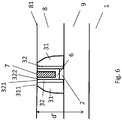
- Fig. 6 illustrates that embodiments of the present invention are also applicable in the context of non-planar devices, as for instance FINFET device or other devices wherein the active layer or region 9 protrudes from the front surface of the substrate.
- the active layer can for instance be provided as a FIN structure 9 on top of a front surface of a substrate 1.
- the dummy gate structure or final gate structure can then be provided at least partially on top of the active region, and can be provided around the protruding region (e.g. FIN structure), in a certain view "wrapping" the FIN structure, in first areas.
- the same dummy gate structure or final gate structure can be provided on the substrate 1, while extending adjacent to the FIN structure, for instance towards a further adjacent FIN structure on the substrate.
- the dummy gate structure or final gate structure can be provided on the substrate 1, while extending adjacent to the FIN structure, for instance towards a further adjacent FIN structure on the substrate.
- Embodiments of the present invention may then be even more advantageous.
- an optimal thickness is a thickness of about 5 nm.
- this optimal thickness is expected to be smaller, and can be for instance 4nm.
- an optimal thickness can be 3nm.
- the thickness of the metal layer also called metal source
- a typical combination of diffusion layer/metal layer for instance silicon layer/metal layer, has a thickness combination of 5nm/20nm.
Landscapes
- Engineering & Computer Science (AREA)
- Physics & Mathematics (AREA)
- Condensed Matter Physics & Semiconductors (AREA)
- General Physics & Mathematics (AREA)
- Manufacturing & Machinery (AREA)
- Computer Hardware Design (AREA)
- Microelectronics & Electronic Packaging (AREA)
- Power Engineering (AREA)
- Insulated Gate Type Field-Effect Transistor (AREA)
- Electrodes Of Semiconductors (AREA)
- Metal-Oxide And Bipolar Metal-Oxide Semiconductor Integrated Circuits (AREA)
- Thin Film Transistor (AREA)
Claims (11)
- Verfahren zur Herstellung eines Feldeffekttransistors, das Verfahren umfassend die Schritte:- Bereitstellen einer Dummy-Gate-Struktur auf einem Substrat (1), wobei die Dummy-Gate-Struktur eine Gate-Dielektrikum-Schicht (2) und eine Dummy-Gate-Elektrodenschicht umfasst, wobei die Dummy-Gate-Struktur seitlich durch einen Gategraben definiert ist, welcher durch Innenseitenwände einer Gruppe von Abstandhaltern (31, 32) definiert ist;- seitliches Einbetten der Dummy-Gate-Struktur mittels einer oder mehrerer Einbettungsschichten (8), wobei die eine oder mehreren Einbettungsschichten eine Vorderfläche (81) definieren;- Entfernen der Dummy-Gate-Elektrodenschicht zwischen den Innenseitenwänden (322) der Gruppe von Abstandhaltern (31, 32);- Bereitstellen einer finalen Gate-Elektrodenschicht, welche die Dummy-Gate-Elektrodenschicht zwischen den Innenseitenwänden (322) der Gruppe von Abstandhaltern (31, 32) ersetzt;wobei der horizontale Abstand zwischen den Innenseitenwänden (322) der Abstandhalter geringer als 20 nm ist;
wobei das Bereitstellen einer finalen Gate-Elektrodenschicht umfasst:- Bereitstellen einer durchgängigen Diffusionsschicht (4), wobei sich die Diffusionsschicht (4) zumindest oben auf der Gate-Dielektrikum-Schicht (2), an Innenseitenwänden der Gruppe von Abstandhaltern (31, 32) und zumindest auf einem Abschnitt der Vorderfläche (81) erstreckt;- Bereitstellen einer Metallschicht (5), die ein Metall umfasst, oben auf der Diffusionsschicht (4), auf der Vorderfläche und wobei das Metall nicht in den Gategraben eintritt;- Anwenden eines Glühschritts, wobei der Glühschritt zum Antreiben der Diffusion des Metalls der Metallschicht (5) in die Diffusionsschicht (4) ausgelegt ist, und zum weiteren Diffundieren des Metalls in der Diffusionsschicht hin zu dem Abschnitt der Diffusionsschicht in dem Bereich, der dem Bereich des Gate-Dielektrikums (2) entspricht;- Füllen des Bereichs zwischen den Innenseitenwänden der Gruppe von Abstandhaltern mit einer finalen Gate-Metallfüllschicht. - Verfahren nach Anspruch 1, wobei die Diffusionsschicht (4) Silicium umfasst.
- Verfahren nach einem der vorstehenden Ansprüche, wobei die Diffusionsschicht (4) eine Dicke im Bereich von 2 bis 10 nm aufweist.
- Verfahren nach einem der vorstehenden Ansprüche, wobei die Metallschicht (5) Aluminium, Indium, Gallium oder Nickel umfasst.
- Verfahren nach einem der vorstehenden Ansprüche, wobei der Glühschritt bei einer Temperatur zwischen 400 °C und 600 °C durchgeführt wird.
- Verfahren nach einem der vorstehenden Ansprüche, wobei der Glühschritt eine Dauer von 1 bis 10 Minuten aufweist.
- Verfahren nach einem der vorstehenden Ansprüche, wobei ein vertikaler Abstand zwischen der Metallschicht auf der Vorderfläche und einer oberen Fläche der Diffusionsschicht in einem Bereich oben auf der Gate-Dielektrikum-Schicht geringer als 170 nm ist.
- Verfahren nach einem der vorstehenden Ansprüche, wobei die Diffusionsschicht (4) mittels chemischer Gasphasenabscheidung (CVD) abgeschieden wird.
- Verfahren nach einem der vorstehenden Ansprüche, wobei der Glühschritt von solcher Art ist, dass sich die Diffusionsschicht (4) und die Metallschicht (5) vollständig zu einer einzelnen vereinten Schicht (6) mit gemischter Beschaffenheit vereinen.
- Verfahren nach einem der vorstehenden Ansprüche, weiter umfassend Durchführen eines Schritts eines chemisch-mechanischen Polierens (CMP) nach dem Anwenden des Glühschritts und Füllen des Bereichs zwischen den Innenseitenwänden (322) der Gruppe von Abstandhaltern mit einer finalen Gate-Metallfüllschicht.
- Verfahren nach einem der vorstehenden Ansprüche, wobei der Feldeffekttransistor vom nicht-planaren Typ ist und mindestens eine FIN-Struktur umfasst, die von einer Vorderfläche des Substrats vorsteht, und wobei die Dummy-Gate-Struktur zumindest teilweise auf der FIN-Struktur und zumindest teilweise benachbart zu der FIN-Struktur bereitgestellt ist.
Priority Applications (3)
| Application Number | Priority Date | Filing Date | Title |
|---|---|---|---|
| EP13166902.0A EP2802003B1 (de) | 2013-05-07 | 2013-05-07 | Verfahren zur Bereitstellung einer Gate-Metallschicht einer Transistorvorrichtung |
| JP2014086568A JP6158132B2 (ja) | 2013-05-07 | 2014-04-18 | トランジスタデバイスのゲート金属層を設ける方法および関連するトランジスタ |
| US14/271,956 US9202695B2 (en) | 2013-05-07 | 2014-05-07 | Method for providing a gate metal layer of a transistor device and associated transistor |
Applications Claiming Priority (1)
| Application Number | Priority Date | Filing Date | Title |
|---|---|---|---|
| EP13166902.0A EP2802003B1 (de) | 2013-05-07 | 2013-05-07 | Verfahren zur Bereitstellung einer Gate-Metallschicht einer Transistorvorrichtung |
Publications (2)
| Publication Number | Publication Date |
|---|---|
| EP2802003A1 EP2802003A1 (de) | 2014-11-12 |
| EP2802003B1 true EP2802003B1 (de) | 2019-08-28 |
Family
ID=48227076
Family Applications (1)
| Application Number | Title | Priority Date | Filing Date |
|---|---|---|---|
| EP13166902.0A Active EP2802003B1 (de) | 2013-05-07 | 2013-05-07 | Verfahren zur Bereitstellung einer Gate-Metallschicht einer Transistorvorrichtung |
Country Status (3)
| Country | Link |
|---|---|
| US (1) | US9202695B2 (de) |
| EP (1) | EP2802003B1 (de) |
| JP (1) | JP6158132B2 (de) |
Families Citing this family (5)
| Publication number | Priority date | Publication date | Assignee | Title |
|---|---|---|---|---|
| WO2016063743A1 (ja) | 2014-10-23 | 2016-04-28 | 株式会社Screenホールディングス | 熱処理方法および熱処理装置 |
| CN108962892B (zh) * | 2017-05-26 | 2021-02-26 | 联华电子股份有限公司 | 半导体元件及其制作方法 |
| US10204828B1 (en) | 2018-02-09 | 2019-02-12 | International Business Machines Corporation | Enabling low resistance gates and contacts integrated with bilayer dielectrics |
| US10529823B2 (en) | 2018-05-29 | 2020-01-07 | International Business Machines Corporation | Method of manufacturing a semiconductor device having a metal gate with different lateral widths between spacers |
| US11978774B2 (en) * | 2020-10-05 | 2024-05-07 | Sandisk Technologies Llc | High voltage field effect transistor with vertical current paths and method of making the same |
Family Cites Families (12)
| Publication number | Priority date | Publication date | Assignee | Title |
|---|---|---|---|---|
| JPH08255766A (ja) * | 1995-03-17 | 1996-10-01 | Sony Corp | 半導体装置の製造方法 |
| JP2002299610A (ja) * | 2001-03-30 | 2002-10-11 | Toshiba Corp | 半導体装置およびその製造方法 |
| FR2844396B1 (fr) * | 2002-09-06 | 2006-02-03 | St Microelectronics Sa | Procede de realisation d'un composant electronique integre et dispositif electrique incorporant un composant integre ainsi obtenu |
| US7071086B2 (en) * | 2003-04-23 | 2006-07-04 | Advanced Micro Devices, Inc. | Method of forming a metal gate structure with tuning of work function by silicon incorporation |
| US7268065B2 (en) * | 2004-06-18 | 2007-09-11 | Taiwan Semiconductor Manufacturing Company, Ltd. | Methods of manufacturing metal-silicide features |
| US7091118B1 (en) | 2004-11-16 | 2006-08-15 | Advanced Micro Devices, Inc. | Replacement metal gate transistor with metal-rich silicon layer and method for making the same |
| US8294202B2 (en) * | 2009-07-08 | 2012-10-23 | Taiwan Semiconductor Manufacturing Company, Ltd. | Metal gate structure of a semiconductor device |
| US8304841B2 (en) * | 2009-09-14 | 2012-11-06 | Taiwan Semiconductor Manufacturing Company, Ltd. | Metal gate transistor, integrated circuits, systems, and fabrication methods thereof |
| JP5598145B2 (ja) * | 2010-08-04 | 2014-10-01 | 富士通セミコンダクター株式会社 | 半導体装置の製造方法及び半導体装置 |
| US8492286B2 (en) | 2010-11-22 | 2013-07-23 | International Business Machines Corporation | Method of forming E-fuse in replacement metal gate manufacturing process |
| US8450169B2 (en) | 2010-11-29 | 2013-05-28 | International Business Machines Corporation | Replacement metal gate structures providing independent control on work function and gate leakage current |
| US20120135590A1 (en) | 2010-11-30 | 2012-05-31 | Advanced Technology Materials, Inc. | Silicon removal from surfaces and method of forming high k metal gate structures using same |
-
2013
- 2013-05-07 EP EP13166902.0A patent/EP2802003B1/de active Active
-
2014
- 2014-04-18 JP JP2014086568A patent/JP6158132B2/ja active Active
- 2014-05-07 US US14/271,956 patent/US9202695B2/en active Active
Non-Patent Citations (1)
| Title |
|---|
| None * |
Also Published As
| Publication number | Publication date |
|---|---|
| JP2014220496A (ja) | 2014-11-20 |
| US20140332864A1 (en) | 2014-11-13 |
| US9202695B2 (en) | 2015-12-01 |
| EP2802003A1 (de) | 2014-11-12 |
| JP6158132B2 (ja) | 2017-07-05 |
Similar Documents
| Publication | Publication Date | Title |
|---|---|---|
| US9391075B2 (en) | Integrated circuit and method for fabricating the same having a replacement gate structure | |
| US10872893B2 (en) | Dual nitride stressor for semiconductor device and method of manufacturing | |
| CN103247535B (zh) | Finfet器件及其形成方法 | |
| US9287273B2 (en) | Method for manufacturing a semiconductor device comprising transistors each having a different effective work function | |
| CN103972097B (zh) | 制造FinFET器件的方法 | |
| CN106328589B (zh) | 在氧化物衬底上的FinFET沟道和相关方法 | |
| US9698058B2 (en) | Structure and method for FinFET device | |
| CN109585373B (zh) | 具有可控气隙的finfet结构 | |
| TWI604516B (zh) | 半導體裝置及其製造方法 | |
| CN112599591B (zh) | Finfet掺杂结构 | |
| US20130043517A1 (en) | Semiconductor Structure And Method For Manufacturing The Same | |
| KR102277762B1 (ko) | 반도체 디바이스 및 제조 방법 | |
| CN106328539A (zh) | 多栅极器件及其制造方法 | |
| CN105280706B (zh) | 具有栅极氧化物层的finfet器件 | |
| CN105977144A (zh) | FinFET沟道的形成方法及其结构 | |
| US10276574B2 (en) | Semiconductor device and manufacturing method thereof | |
| US20150221768A1 (en) | Semiconductor structure and method for manufacturing the same | |
| CN106409679A (zh) | 具有掺杂的隔离绝缘层的鳍式场效应晶体管 | |
| CN102437118B (zh) | 具有金属栅极的晶体管的制作方法 | |
| TW201543679A (zh) | 半導體裝置結構及其製造方法 | |
| EP2802003B1 (de) | Verfahren zur Bereitstellung einer Gate-Metallschicht einer Transistorvorrichtung | |
| TW201740475A (zh) | 半導體元件及其製作方法 | |
| CN103779224A (zh) | Mosfet的制造方法 | |
| CN104952797B (zh) | 一种半导体器件的制备方法 | |
| CN104183496B (zh) | 鳍式场效应晶体管器件的制造方法 |
Legal Events
| Date | Code | Title | Description |
|---|---|---|---|
| PUAI | Public reference made under article 153(3) epc to a published international application that has entered the european phase |
Free format text: ORIGINAL CODE: 0009012 |
|
| 17P | Request for examination filed |
Effective date: 20130507 |
|
| AK | Designated contracting states |
Kind code of ref document: A1 Designated state(s): AL AT BE BG CH CY CZ DE DK EE ES FI FR GB GR HR HU IE IS IT LI LT LU LV MC MK MT NL NO PL PT RO RS SE SI SK SM TR |
|
| AX | Request for extension of the european patent |
Extension state: BA ME |
|
| R17P | Request for examination filed (corrected) |
Effective date: 20150423 |
|
| RBV | Designated contracting states (corrected) |
Designated state(s): AL AT BE BG CH CY CZ DE DK EE ES FI FR GB GR HR HU IE IS IT LI LT LU LV MC MK MT NL NO PL PT RO RS SE SI SK SM TR |
|
| STAA | Information on the status of an ep patent application or granted ep patent |
Free format text: STATUS: EXAMINATION IS IN PROGRESS |
|
| 17Q | First examination report despatched |
Effective date: 20171109 |
|
| RAP1 | Party data changed (applicant data changed or rights of an application transferred) |
Owner name: IMEC VZW |
|
| GRAP | Despatch of communication of intention to grant a patent |
Free format text: ORIGINAL CODE: EPIDOSNIGR1 |
|
| STAA | Information on the status of an ep patent application or granted ep patent |
Free format text: STATUS: GRANT OF PATENT IS INTENDED |
|
| INTG | Intention to grant announced |
Effective date: 20190425 |
|
| GRAS | Grant fee paid |
Free format text: ORIGINAL CODE: EPIDOSNIGR3 |
|
| GRAA | (expected) grant |
Free format text: ORIGINAL CODE: 0009210 |
|
| STAA | Information on the status of an ep patent application or granted ep patent |
Free format text: STATUS: THE PATENT HAS BEEN GRANTED |
|
| AK | Designated contracting states |
Kind code of ref document: B1 Designated state(s): AL AT BE BG CH CY CZ DE DK EE ES FI FR GB GR HR HU IE IS IT LI LT LU LV MC MK MT NL NO PL PT RO RS SE SI SK SM TR |
|
| REG | Reference to a national code |
Ref country code: GB Ref legal event code: FG4D |
|
| REG | Reference to a national code |
Ref country code: CH Ref legal event code: EP |
|
| REG | Reference to a national code |
Ref country code: AT Ref legal event code: REF Ref document number: 1173448 Country of ref document: AT Kind code of ref document: T Effective date: 20190915 |
|
| REG | Reference to a national code |
Ref country code: IE Ref legal event code: FG4D |
|
| REG | Reference to a national code |
Ref country code: DE Ref legal event code: R096 Ref document number: 602013059654 Country of ref document: DE |
|
| REG | Reference to a national code |
Ref country code: NL Ref legal event code: MP Effective date: 20190828 |
|
| REG | Reference to a national code |
Ref country code: LT Ref legal event code: MG4D |
|
| PG25 | Lapsed in a contracting state [announced via postgrant information from national office to epo] |
Ref country code: SE Free format text: LAPSE BECAUSE OF FAILURE TO SUBMIT A TRANSLATION OF THE DESCRIPTION OR TO PAY THE FEE WITHIN THE PRESCRIBED TIME-LIMIT Effective date: 20190828 Ref country code: HR Free format text: LAPSE BECAUSE OF FAILURE TO SUBMIT A TRANSLATION OF THE DESCRIPTION OR TO PAY THE FEE WITHIN THE PRESCRIBED TIME-LIMIT Effective date: 20190828 Ref country code: PT Free format text: LAPSE BECAUSE OF FAILURE TO SUBMIT A TRANSLATION OF THE DESCRIPTION OR TO PAY THE FEE WITHIN THE PRESCRIBED TIME-LIMIT Effective date: 20191230 Ref country code: NL Free format text: LAPSE BECAUSE OF FAILURE TO SUBMIT A TRANSLATION OF THE DESCRIPTION OR TO PAY THE FEE WITHIN THE PRESCRIBED TIME-LIMIT Effective date: 20190828 Ref country code: FI Free format text: LAPSE BECAUSE OF FAILURE TO SUBMIT A TRANSLATION OF THE DESCRIPTION OR TO PAY THE FEE WITHIN THE PRESCRIBED TIME-LIMIT Effective date: 20190828 Ref country code: LT Free format text: LAPSE BECAUSE OF FAILURE TO SUBMIT A TRANSLATION OF THE DESCRIPTION OR TO PAY THE FEE WITHIN THE PRESCRIBED TIME-LIMIT Effective date: 20190828 Ref country code: BG Free format text: LAPSE BECAUSE OF FAILURE TO SUBMIT A TRANSLATION OF THE DESCRIPTION OR TO PAY THE FEE WITHIN THE PRESCRIBED TIME-LIMIT Effective date: 20191128 Ref country code: NO Free format text: LAPSE BECAUSE OF FAILURE TO SUBMIT A TRANSLATION OF THE DESCRIPTION OR TO PAY THE FEE WITHIN THE PRESCRIBED TIME-LIMIT Effective date: 20191128 |
|
| PG25 | Lapsed in a contracting state [announced via postgrant information from national office to epo] |
Ref country code: AL Free format text: LAPSE BECAUSE OF FAILURE TO SUBMIT A TRANSLATION OF THE DESCRIPTION OR TO PAY THE FEE WITHIN THE PRESCRIBED TIME-LIMIT Effective date: 20190828 Ref country code: ES Free format text: LAPSE BECAUSE OF FAILURE TO SUBMIT A TRANSLATION OF THE DESCRIPTION OR TO PAY THE FEE WITHIN THE PRESCRIBED TIME-LIMIT Effective date: 20190828 Ref country code: RS Free format text: LAPSE BECAUSE OF FAILURE TO SUBMIT A TRANSLATION OF THE DESCRIPTION OR TO PAY THE FEE WITHIN THE PRESCRIBED TIME-LIMIT Effective date: 20190828 Ref country code: IS Free format text: LAPSE BECAUSE OF FAILURE TO SUBMIT A TRANSLATION OF THE DESCRIPTION OR TO PAY THE FEE WITHIN THE PRESCRIBED TIME-LIMIT Effective date: 20191228 Ref country code: LV Free format text: LAPSE BECAUSE OF FAILURE TO SUBMIT A TRANSLATION OF THE DESCRIPTION OR TO PAY THE FEE WITHIN THE PRESCRIBED TIME-LIMIT Effective date: 20190828 Ref country code: GR Free format text: LAPSE BECAUSE OF FAILURE TO SUBMIT A TRANSLATION OF THE DESCRIPTION OR TO PAY THE FEE WITHIN THE PRESCRIBED TIME-LIMIT Effective date: 20191129 |
|
| REG | Reference to a national code |
Ref country code: AT Ref legal event code: MK05 Ref document number: 1173448 Country of ref document: AT Kind code of ref document: T Effective date: 20190828 |
|
| PG25 | Lapsed in a contracting state [announced via postgrant information from national office to epo] |
Ref country code: TR Free format text: LAPSE BECAUSE OF FAILURE TO SUBMIT A TRANSLATION OF THE DESCRIPTION OR TO PAY THE FEE WITHIN THE PRESCRIBED TIME-LIMIT Effective date: 20190828 |
|
| PG25 | Lapsed in a contracting state [announced via postgrant information from national office to epo] |
Ref country code: RO Free format text: LAPSE BECAUSE OF FAILURE TO SUBMIT A TRANSLATION OF THE DESCRIPTION OR TO PAY THE FEE WITHIN THE PRESCRIBED TIME-LIMIT Effective date: 20190828 Ref country code: IT Free format text: LAPSE BECAUSE OF FAILURE TO SUBMIT A TRANSLATION OF THE DESCRIPTION OR TO PAY THE FEE WITHIN THE PRESCRIBED TIME-LIMIT Effective date: 20190828 Ref country code: DK Free format text: LAPSE BECAUSE OF FAILURE TO SUBMIT A TRANSLATION OF THE DESCRIPTION OR TO PAY THE FEE WITHIN THE PRESCRIBED TIME-LIMIT Effective date: 20190828 Ref country code: EE Free format text: LAPSE BECAUSE OF FAILURE TO SUBMIT A TRANSLATION OF THE DESCRIPTION OR TO PAY THE FEE WITHIN THE PRESCRIBED TIME-LIMIT Effective date: 20190828 Ref country code: PL Free format text: LAPSE BECAUSE OF FAILURE TO SUBMIT A TRANSLATION OF THE DESCRIPTION OR TO PAY THE FEE WITHIN THE PRESCRIBED TIME-LIMIT Effective date: 20190828 Ref country code: AT Free format text: LAPSE BECAUSE OF FAILURE TO SUBMIT A TRANSLATION OF THE DESCRIPTION OR TO PAY THE FEE WITHIN THE PRESCRIBED TIME-LIMIT Effective date: 20190828 |
|
| PG25 | Lapsed in a contracting state [announced via postgrant information from national office to epo] |
Ref country code: CZ Free format text: LAPSE BECAUSE OF FAILURE TO SUBMIT A TRANSLATION OF THE DESCRIPTION OR TO PAY THE FEE WITHIN THE PRESCRIBED TIME-LIMIT Effective date: 20190828 Ref country code: SK Free format text: LAPSE BECAUSE OF FAILURE TO SUBMIT A TRANSLATION OF THE DESCRIPTION OR TO PAY THE FEE WITHIN THE PRESCRIBED TIME-LIMIT Effective date: 20190828 Ref country code: IS Free format text: LAPSE BECAUSE OF FAILURE TO SUBMIT A TRANSLATION OF THE DESCRIPTION OR TO PAY THE FEE WITHIN THE PRESCRIBED TIME-LIMIT Effective date: 20200224 Ref country code: SM Free format text: LAPSE BECAUSE OF FAILURE TO SUBMIT A TRANSLATION OF THE DESCRIPTION OR TO PAY THE FEE WITHIN THE PRESCRIBED TIME-LIMIT Effective date: 20190828 |
|
| REG | Reference to a national code |
Ref country code: DE Ref legal event code: R097 Ref document number: 602013059654 Country of ref document: DE |
|
| PLBE | No opposition filed within time limit |
Free format text: ORIGINAL CODE: 0009261 |
|
| STAA | Information on the status of an ep patent application or granted ep patent |
Free format text: STATUS: NO OPPOSITION FILED WITHIN TIME LIMIT |
|
| PG2D | Information on lapse in contracting state deleted |
Ref country code: IS |
|
| 26N | No opposition filed |
Effective date: 20200603 |
|
| PG25 | Lapsed in a contracting state [announced via postgrant information from national office to epo] |
Ref country code: SI Free format text: LAPSE BECAUSE OF FAILURE TO SUBMIT A TRANSLATION OF THE DESCRIPTION OR TO PAY THE FEE WITHIN THE PRESCRIBED TIME-LIMIT Effective date: 20190828 |
|
| PG25 | Lapsed in a contracting state [announced via postgrant information from national office to epo] |
Ref country code: MC Free format text: LAPSE BECAUSE OF FAILURE TO SUBMIT A TRANSLATION OF THE DESCRIPTION OR TO PAY THE FEE WITHIN THE PRESCRIBED TIME-LIMIT Effective date: 20190828 Ref country code: LI Free format text: LAPSE BECAUSE OF NON-PAYMENT OF DUE FEES Effective date: 20200531 Ref country code: CH Free format text: LAPSE BECAUSE OF NON-PAYMENT OF DUE FEES Effective date: 20200531 |
|
| REG | Reference to a national code |
Ref country code: BE Ref legal event code: MM Effective date: 20200531 |
|
| GBPC | Gb: european patent ceased through non-payment of renewal fee |
Effective date: 20200507 |
|
| PG25 | Lapsed in a contracting state [announced via postgrant information from national office to epo] |
Ref country code: LU Free format text: LAPSE BECAUSE OF NON-PAYMENT OF DUE FEES Effective date: 20200507 |
|
| PG25 | Lapsed in a contracting state [announced via postgrant information from national office to epo] |
Ref country code: GB Free format text: LAPSE BECAUSE OF NON-PAYMENT OF DUE FEES Effective date: 20200507 Ref country code: IE Free format text: LAPSE BECAUSE OF NON-PAYMENT OF DUE FEES Effective date: 20200507 |
|
| PG25 | Lapsed in a contracting state [announced via postgrant information from national office to epo] |
Ref country code: BE Free format text: LAPSE BECAUSE OF NON-PAYMENT OF DUE FEES Effective date: 20200531 |
|
| PG25 | Lapsed in a contracting state [announced via postgrant information from national office to epo] |
Ref country code: MT Free format text: LAPSE BECAUSE OF FAILURE TO SUBMIT A TRANSLATION OF THE DESCRIPTION OR TO PAY THE FEE WITHIN THE PRESCRIBED TIME-LIMIT Effective date: 20190828 Ref country code: CY Free format text: LAPSE BECAUSE OF FAILURE TO SUBMIT A TRANSLATION OF THE DESCRIPTION OR TO PAY THE FEE WITHIN THE PRESCRIBED TIME-LIMIT Effective date: 20190828 |
|
| PG25 | Lapsed in a contracting state [announced via postgrant information from national office to epo] |
Ref country code: MK Free format text: LAPSE BECAUSE OF FAILURE TO SUBMIT A TRANSLATION OF THE DESCRIPTION OR TO PAY THE FEE WITHIN THE PRESCRIBED TIME-LIMIT Effective date: 20190828 |
|
| P01 | Opt-out of the competence of the unified patent court (upc) registered |
Effective date: 20230513 |
|
| REG | Reference to a national code |
Ref country code: DE Ref legal event code: R079 Ref document number: 602013059654 Country of ref document: DE Free format text: PREVIOUS MAIN CLASS: H01L0021280000 Ipc: H10D0064010000 |
|
| PGFP | Annual fee paid to national office [announced via postgrant information from national office to epo] |
Ref country code: DE Payment date: 20250423 Year of fee payment: 13 |
|
| PGFP | Annual fee paid to national office [announced via postgrant information from national office to epo] |
Ref country code: FR Payment date: 20250423 Year of fee payment: 13 |