EP2797092A1 - Magnetic field shielding sheet for a wireless charger, method for manufacturing same, and receiving apparatus for a wireless charger using the sheet - Google Patents
Magnetic field shielding sheet for a wireless charger, method for manufacturing same, and receiving apparatus for a wireless charger using the sheet Download PDFInfo
- Publication number
- EP2797092A1 EP2797092A1 EP12859492.6A EP12859492A EP2797092A1 EP 2797092 A1 EP2797092 A1 EP 2797092A1 EP 12859492 A EP12859492 A EP 12859492A EP 2797092 A1 EP2797092 A1 EP 2797092A1
- Authority
- EP
- European Patent Office
- Prior art keywords
- sheet
- magnetic field
- magnetic
- wireless charger
- field shield
- Prior art date
- Legal status (The legal status is an assumption and is not a legal conclusion. Google has not performed a legal analysis and makes no representation as to the accuracy of the status listed.)
- Granted
Links
Images





Classifications
-
- H—ELECTRICITY
- H01—ELECTRIC ELEMENTS
- H01F—MAGNETS; INDUCTANCES; TRANSFORMERS; SELECTION OF MATERIALS FOR THEIR MAGNETIC PROPERTIES
- H01F27/00—Details of transformers or inductances, in general
- H01F27/34—Special means for preventing or reducing unwanted electric or magnetic effects, e.g. no-load losses, reactive currents, harmonics, oscillations, leakage fields
- H01F27/36—Electric or magnetic shields or screens
-
- B—PERFORMING OPERATIONS; TRANSPORTING
- B32—LAYERED PRODUCTS
- B32B—LAYERED PRODUCTS, i.e. PRODUCTS BUILT-UP OF STRATA OF FLAT OR NON-FLAT, e.g. CELLULAR OR HONEYCOMB, FORM
- B32B27/00—Layered products comprising a layer of synthetic resin
- B32B27/06—Layered products comprising a layer of synthetic resin as the main or only constituent of a layer, which is next to another layer of the same or of a different material
- B32B27/08—Layered products comprising a layer of synthetic resin as the main or only constituent of a layer, which is next to another layer of the same or of a different material of synthetic resin
-
- B—PERFORMING OPERATIONS; TRANSPORTING
- B32—LAYERED PRODUCTS
- B32B—LAYERED PRODUCTS, i.e. PRODUCTS BUILT-UP OF STRATA OF FLAT OR NON-FLAT, e.g. CELLULAR OR HONEYCOMB, FORM
- B32B37/00—Methods or apparatus for laminating, e.g. by curing or by ultrasonic bonding
- B32B37/12—Methods or apparatus for laminating, e.g. by curing or by ultrasonic bonding characterised by using adhesives
-
- B—PERFORMING OPERATIONS; TRANSPORTING
- B32—LAYERED PRODUCTS
- B32B—LAYERED PRODUCTS, i.e. PRODUCTS BUILT-UP OF STRATA OF FLAT OR NON-FLAT, e.g. CELLULAR OR HONEYCOMB, FORM
- B32B37/00—Methods or apparatus for laminating, e.g. by curing or by ultrasonic bonding
- B32B37/14—Methods or apparatus for laminating, e.g. by curing or by ultrasonic bonding characterised by the properties of the layers
- B32B37/16—Methods or apparatus for laminating, e.g. by curing or by ultrasonic bonding characterised by the properties of the layers with all layers existing as coherent layers before laminating
- B32B37/18—Methods or apparatus for laminating, e.g. by curing or by ultrasonic bonding characterised by the properties of the layers with all layers existing as coherent layers before laminating involving the assembly of discrete sheets or panels only
-
- B—PERFORMING OPERATIONS; TRANSPORTING
- B32—LAYERED PRODUCTS
- B32B—LAYERED PRODUCTS, i.e. PRODUCTS BUILT-UP OF STRATA OF FLAT OR NON-FLAT, e.g. CELLULAR OR HONEYCOMB, FORM
- B32B38/00—Ancillary operations in connection with laminating processes
- B32B38/0004—Cutting, tearing or severing, e.g. bursting; Cutter details
-
- H—ELECTRICITY
- H01—ELECTRIC ELEMENTS
- H01F—MAGNETS; INDUCTANCES; TRANSFORMERS; SELECTION OF MATERIALS FOR THEIR MAGNETIC PROPERTIES
- H01F27/00—Details of transformers or inductances, in general
- H01F27/34—Special means for preventing or reducing unwanted electric or magnetic effects, e.g. no-load losses, reactive currents, harmonics, oscillations, leakage fields
- H01F27/36—Electric or magnetic shields or screens
- H01F27/366—Electric or magnetic shields or screens made of ferromagnetic material
-
- H—ELECTRICITY
- H01—ELECTRIC ELEMENTS
- H01F—MAGNETS; INDUCTANCES; TRANSFORMERS; SELECTION OF MATERIALS FOR THEIR MAGNETIC PROPERTIES
- H01F38/00—Adaptations of transformers or inductances for specific applications or functions
- H01F38/14—Inductive couplings
-
- H—ELECTRICITY
- H01—ELECTRIC ELEMENTS
- H01Q—ANTENNAS, i.e. RADIO AERIALS
- H01Q7/00—Loop antennas with a substantially uniform current distribution around the loop and having a directional radiation pattern in a plane perpendicular to the plane of the loop
- H01Q7/06—Loop antennas with a substantially uniform current distribution around the loop and having a directional radiation pattern in a plane perpendicular to the plane of the loop with core of ferromagnetic material
-
- H—ELECTRICITY
- H01—ELECTRIC ELEMENTS
- H01Q—ANTENNAS, i.e. RADIO AERIALS
- H01Q7/00—Loop antennas with a substantially uniform current distribution around the loop and having a directional radiation pattern in a plane perpendicular to the plane of the loop
- H01Q7/06—Loop antennas with a substantially uniform current distribution around the loop and having a directional radiation pattern in a plane perpendicular to the plane of the loop with core of ferromagnetic material
- H01Q7/08—Ferrite rod or like elongated core
-
- H—ELECTRICITY
- H02—GENERATION; CONVERSION OR DISTRIBUTION OF ELECTRIC POWER
- H02J—ELECTRIC POWER NETWORKS; CIRCUIT ARRANGEMENTS OR SYSTEMS FOR SUPPLYING OR DISTRIBUTING ELECTRIC POWER; SYSTEMS FOR STORING ELECTRIC ENERGY
- H02J50/00—Circuit arrangements or systems for wireless supply or distribution of electric power
- H02J50/10—Circuit arrangements or systems for wireless supply or distribution of electric power using inductive coupling
-
- H—ELECTRICITY
- H02—GENERATION; CONVERSION OR DISTRIBUTION OF ELECTRIC POWER
- H02J—ELECTRIC POWER NETWORKS; CIRCUIT ARRANGEMENTS OR SYSTEMS FOR SUPPLYING OR DISTRIBUTING ELECTRIC POWER; SYSTEMS FOR STORING ELECTRIC ENERGY
- H02J50/00—Circuit arrangements or systems for wireless supply or distribution of electric power
- H02J50/10—Circuit arrangements or systems for wireless supply or distribution of electric power using inductive coupling
- H02J50/12—Circuit arrangements or systems for wireless supply or distribution of electric power using inductive coupling of the resonant type
-
- H—ELECTRICITY
- H02—GENERATION; CONVERSION OR DISTRIBUTION OF ELECTRIC POWER
- H02J—ELECTRIC POWER NETWORKS; CIRCUIT ARRANGEMENTS OR SYSTEMS FOR SUPPLYING OR DISTRIBUTING ELECTRIC POWER; SYSTEMS FOR STORING ELECTRIC ENERGY
- H02J50/00—Circuit arrangements or systems for wireless supply or distribution of electric power
- H02J50/70—Circuit arrangements or systems for wireless supply or distribution of electric power involving the reduction of electric, magnetic or electromagnetic leakage fields
-
- H—ELECTRICITY
- H02—GENERATION; CONVERSION OR DISTRIBUTION OF ELECTRIC POWER
- H02J—ELECTRIC POWER NETWORKS; CIRCUIT ARRANGEMENTS OR SYSTEMS FOR SUPPLYING OR DISTRIBUTING ELECTRIC POWER; SYSTEMS FOR STORING ELECTRIC ENERGY
- H02J7/00—Circuit arrangements for charging or discharging batteries or for supplying loads from batteries
-
- H—ELECTRICITY
- H02—GENERATION; CONVERSION OR DISTRIBUTION OF ELECTRIC POWER
- H02J—ELECTRIC POWER NETWORKS; CIRCUIT ARRANGEMENTS OR SYSTEMS FOR SUPPLYING OR DISTRIBUTING ELECTRIC POWER; SYSTEMS FOR STORING ELECTRIC ENERGY
- H02J7/00—Circuit arrangements for charging or discharging batteries or for supplying loads from batteries
- H02J7/70—Circuit arrangements for charging or discharging batteries or for supplying loads from batteries characterised by the mechanical construction
-
- H—ELECTRICITY
- H04—ELECTRIC COMMUNICATION TECHNIQUE
- H04B—TRANSMISSION
- H04B5/00—Near-field transmission systems, e.g. inductive or capacitive transmission systems
- H04B5/70—Near-field transmission systems, e.g. inductive or capacitive transmission systems specially adapted for specific purposes
- H04B5/79—Near-field transmission systems, e.g. inductive or capacitive transmission systems specially adapted for specific purposes for data transfer in combination with power transfer
-
- H—ELECTRICITY
- H05—ELECTRIC TECHNIQUES NOT OTHERWISE PROVIDED FOR
- H05K—PRINTED CIRCUITS; CASINGS OR CONSTRUCTIONAL DETAILS OF ELECTRIC APPARATUS; MANUFACTURE OF ASSEMBLAGES OF ELECTRICAL COMPONENTS
- H05K9/00—Screening of apparatus or components against electric or magnetic fields
- H05K9/0073—Shielding materials
- H05K9/0075—Magnetic shielding materials
-
- H—ELECTRICITY
- H05—ELECTRIC TECHNIQUES NOT OTHERWISE PROVIDED FOR
- H05K—PRINTED CIRCUITS; CASINGS OR CONSTRUCTIONAL DETAILS OF ELECTRIC APPARATUS; MANUFACTURE OF ASSEMBLAGES OF ELECTRICAL COMPONENTS
- H05K9/00—Screening of apparatus or components against electric or magnetic fields
- H05K9/0073—Shielding materials
- H05K9/0081—Electromagnetic shielding materials, e.g. EMI, RFI shielding
-
- H—ELECTRICITY
- H05—ELECTRIC TECHNIQUES NOT OTHERWISE PROVIDED FOR
- H05K—PRINTED CIRCUITS; CASINGS OR CONSTRUCTIONAL DETAILS OF ELECTRIC APPARATUS; MANUFACTURE OF ASSEMBLAGES OF ELECTRICAL COMPONENTS
- H05K9/00—Screening of apparatus or components against electric or magnetic fields
- H05K9/0073—Shielding materials
- H05K9/0081—Electromagnetic shielding materials, e.g. EMI, RFI shielding
- H05K9/0088—Electromagnetic shielding materials, e.g. EMI, RFI shielding comprising a plurality of shielding layers; combining different shielding material structure
-
- Y—GENERAL TAGGING OF NEW TECHNOLOGICAL DEVELOPMENTS; GENERAL TAGGING OF CROSS-SECTIONAL TECHNOLOGIES SPANNING OVER SEVERAL SECTIONS OF THE IPC; TECHNICAL SUBJECTS COVERED BY FORMER USPC CROSS-REFERENCE ART COLLECTIONS [XRACs] AND DIGESTS
- Y10—TECHNICAL SUBJECTS COVERED BY FORMER USPC
- Y10T—TECHNICAL SUBJECTS COVERED BY FORMER US CLASSIFICATION
- Y10T156/00—Adhesive bonding and miscellaneous chemical manufacture
- Y10T156/10—Methods of surface bonding and/or assembly therefor
-
- Y—GENERAL TAGGING OF NEW TECHNOLOGICAL DEVELOPMENTS; GENERAL TAGGING OF CROSS-SECTIONAL TECHNOLOGIES SPANNING OVER SEVERAL SECTIONS OF THE IPC; TECHNICAL SUBJECTS COVERED BY FORMER USPC CROSS-REFERENCE ART COLLECTIONS [XRACs] AND DIGESTS
- Y10—TECHNICAL SUBJECTS COVERED BY FORMER USPC
- Y10T—TECHNICAL SUBJECTS COVERED BY FORMER US CLASSIFICATION
- Y10T428/00—Stock material or miscellaneous articles
- Y10T428/249921—Web or sheet containing structurally defined element or component
- Y10T428/249953—Composite having voids in a component [e.g., porous, cellular, etc.]
- Y10T428/249955—Void-containing component partially impregnated with adjacent component
-
- Y—GENERAL TAGGING OF NEW TECHNOLOGICAL DEVELOPMENTS; GENERAL TAGGING OF CROSS-SECTIONAL TECHNOLOGIES SPANNING OVER SEVERAL SECTIONS OF THE IPC; TECHNICAL SUBJECTS COVERED BY FORMER USPC CROSS-REFERENCE ART COLLECTIONS [XRACs] AND DIGESTS
- Y10—TECHNICAL SUBJECTS COVERED BY FORMER USPC
- Y10T—TECHNICAL SUBJECTS COVERED BY FORMER US CLASSIFICATION
- Y10T428/00—Stock material or miscellaneous articles
- Y10T428/249921—Web or sheet containing structurally defined element or component
- Y10T428/249953—Composite having voids in a component [e.g., porous, cellular, etc.]
- Y10T428/249955—Void-containing component partially impregnated with adjacent component
- Y10T428/249956—Void-containing component is inorganic
-
- Y—GENERAL TAGGING OF NEW TECHNOLOGICAL DEVELOPMENTS; GENERAL TAGGING OF CROSS-SECTIONAL TECHNOLOGIES SPANNING OVER SEVERAL SECTIONS OF THE IPC; TECHNICAL SUBJECTS COVERED BY FORMER USPC CROSS-REFERENCE ART COLLECTIONS [XRACs] AND DIGESTS
- Y10—TECHNICAL SUBJECTS COVERED BY FORMER USPC
- Y10T—TECHNICAL SUBJECTS COVERED BY FORMER US CLASSIFICATION
- Y10T428/00—Stock material or miscellaneous articles
- Y10T428/25—Web or sheet containing structurally defined element or component and including a second component containing structurally defined particles
-
- Y—GENERAL TAGGING OF NEW TECHNOLOGICAL DEVELOPMENTS; GENERAL TAGGING OF CROSS-SECTIONAL TECHNOLOGIES SPANNING OVER SEVERAL SECTIONS OF THE IPC; TECHNICAL SUBJECTS COVERED BY FORMER USPC CROSS-REFERENCE ART COLLECTIONS [XRACs] AND DIGESTS
- Y10—TECHNICAL SUBJECTS COVERED BY FORMER USPC
- Y10T—TECHNICAL SUBJECTS COVERED BY FORMER US CLASSIFICATION
- Y10T428/00—Stock material or miscellaneous articles
- Y10T428/28—Web or sheet containing structurally defined element or component and having an adhesive outermost layer
- Y10T428/2848—Three or more layers
-
- Y—GENERAL TAGGING OF NEW TECHNOLOGICAL DEVELOPMENTS; GENERAL TAGGING OF CROSS-SECTIONAL TECHNOLOGIES SPANNING OVER SEVERAL SECTIONS OF THE IPC; TECHNICAL SUBJECTS COVERED BY FORMER USPC CROSS-REFERENCE ART COLLECTIONS [XRACs] AND DIGESTS
- Y10—TECHNICAL SUBJECTS COVERED BY FORMER USPC
- Y10T—TECHNICAL SUBJECTS COVERED BY FORMER US CLASSIFICATION
- Y10T428/00—Stock material or miscellaneous articles
- Y10T428/32—Composite [nonstructural laminate] of inorganic material having metal-compound-containing layer and having defined magnetic layer
Definitions
- the present invention relates to a magnetic field shield sheet for a wireless charger, a method of manufacturing the magnetic field shield sheet, and a receiver for the wireless charger by using the magnetic field shield sheet, and more particularly to a magnetic field shield sheet for a wireless charger, which blocks an effect of an alternating-current magnetic field generated when a charger function for a portable mobile terminal device is implemented in a non-contact wireless manner on a main body of the portable mobile terminal device and exhibits excellent electric power transmission efficiency, a method of manufacturing the magnetic field shield sheet, and a receiver for the wireless charger by using the magnetic field shield sheet.
- the contact type charging method carries out a charging operation by making an electrode of a power reception device in direct contact with an electrode of a power feeding device.
- the contact type charging method is commonly used in a wide range of applications, since a structure of a device implementing the contact type charging method is simple.
- various electronic devices become light in the weight thereof, and accordingly a low contact pressure between electrodes of the power reception device and the power feeding device may cause problems such as charge failure charge error.
- secondary batteries are weak at heat, which needs to prevent the temperature rise of the batteries, and to pay attention to a circuit design so as not to cause overcharge and overdischarge. To cope with these problems, a non-contact type charging method is being considered in recent years.
- the non-contact type charging method is a charging method using an electromagnetic induction principle in which coils are mounted at both sides of the power reception device and the power feeding device.
- a non-contact type charger can be miniaturized by putting a ferrite core to be in a magnetic core and winding coils around the ferrite core. Furthermore, for miniaturization and reduction in thickness, a technique of forming a resin substrate by mixing ferrite powder and amorphous powder and mounting a coil and the like on the resin substrate, has been proposed. However, in the case that a ferrite sheet is processed thinly, the thinly processed ferrite sheet may be easily broken and weak in impact resistance. As a result, there have been problems that defects have occurred in the power reception device due to a fall or collision of the non-contact type charger.
- a planar coil that is formed by printing a metal powder paste as a coil has been employed.
- a structure of strengthening a coupling of a planar coil and a magnetic sheet has been proposed.
- a magnetic body or a magnetic sheet is used as a core material to strengthen the coupling between primary and secondary coils.
- a magnetic body or a magnetic sheet was used as a shielding member on the back of the substrate.
- the magnetic body or the magnetic sheet may have the larger magnetic permeability, and the larger area and thickness, a more effective shielding effect can be obtained.
- a magnetic body such as an amorphous ribbon, a ferrite sheet, or a polymer sheet containing magnetic powder is used as the magnetic field shield sheet.
- An effect of focusing a magnetic field for improving magnetic field shielding performance and additional features may be good in the order of amorphous ribbons, a ferrite sheet, and a polymer sheet containing magnetic powder, with high magnetic permeability.
- a magnetic body or a magnetic sheet with high magnetic permeability and large volume is disposed on the opposite surface to a primary coil side, i.e., on the surface of a secondary coil, for reinforcement of a coupling for improving transmission efficiency, and for improving a shielding performance for suppression of heat generation.
- fluctuations in the inductance of the primary coil become large, and an operation condition of a resonant circuit is shifted from a resonance condition at which a sufficient effect can be exhibited according to a relative positional relationship between the magnetic body and the primary coil.
- Korean Patent Application Publication No. 10-2010-31139 provides a power reception device for improving a resonance performance and also suppressing heat generation to solve the aforementioned problems, and proposes a technique of enabling large transmission power and shortening charge time, through an the electronic device and a power reception system using the power reception device.
- a composite magnetic body including a plurality of magnetic sheets magnetic ribbons are arranged at at least one location between a spiral coil a power reception-side spiral coil: a secondary coil and a secondary battery, and between a rectifier and the spiral coil, to thereby prevent a magnetic flux generated from the power reception-side spiral coil from interlinking a circuit board and a secondary battery, and to thereby suppress noise and heat generation caused by an induced electromotive force electromagnetic induction, and the amount of fluctuation of inductance in the primary coil is controlled due to presence or absence of the secondary coil to thus enhance a resonance performance of a resonant circuit constituted by the primary coil and to thereby effectively control oscillation.
- the composite magnetic body is set so that the first magnetoresistance of a first magnetic sheet adjacent to the spiral coil is less than or equal to 60, the second magnetoresistance of a second magnetic sheet laminated on the first magnetic sheet is greater than or equal to 100, and a value of the second magnetoresistance divided by the first magnetoresistance is equal to or greater than 1.0.
- the first magnetic sheet is prepared by bonding polycarbonate resins on both surfaces of a first amorphous ribbon by using adhesive layers, respectively, and the second magnetic sheet is prepared by bonding polycarbonate resins on both surfaces of a second amorphous ribbon with large relative permeability by using adhesive layers, respectively. Then, the first magnetic sheet and the second magnetic sheet are integrally bonded via an adhesive layer.
- the ferrite sheet or a polymer sheet containing magnetic powder has the magnetic permeability a little lower than the amorphous ribbon, and thus in order to improve the performance of such low magnetic permeability, thickness of the ferrite sheet or a polymer sheet becomes large compared to the thin amorphous ribbon of several tens ⁇ m. Therefore, it is difficult to respond to a thinning tendency of terminals.
- the ribbon itself is a metal thin plate, and thus there is no burden on thickness of the amorphous ribbon.
- the functionality of applications may be reduced due to an influence of eddy currents of the ribbon surface, or problems of reducing wireless charging efficiency and causing heat generation may occur.
- Co-based or Fe-based amorphous ribbons can increase surface resistance slightly, through heat treatment.
- a processing treatment such as a flake treatment process of reducing a surface area of the ribbon is performed in order to further reduce the eddy current effects, the magnetic permeability is significantly degraded and the function as the shield sheet is greatly degraded.
- most of wireless chargers employ a structure of adopting permanent magnets that assist an alignment with a power receiver in a power transmitter for power transmission, in order to increase the power transfer efficiency of the chargers to the maximum.
- a magnetization or saturation phenomenon occurs in a thin shield sheet due to a direct-current magnetic field of the permanent magnets, to thereby decrease the performance of the chargers or sharply decreasing the power transmission efficiency.
- the thickness of the shield sheet must be quite thick in the order of 0.5T or higher, in order to indicate shielding features without being affected by the permanent magnets, and to maintain high power transmission efficiency, which may cause a major obstacle on slimming of portable terminals.
- a voltage induced in a secondary coil of a wireless charger is determined by the Fara-day's law and the Lenz's law, and thus it is more advantageous to have the greater amount of magnetic flux linked with the secondary coil in order to obtain a high voltage signal.
- the amount of the magnetic flux becomes large as the amount of a soft magnetic material contained in the secondary coil becomes large and the magnetic permeability of the material becomes high.
- a magnetic field shield sheet in which the secondary coil is mounted is needed to be made of a magnetic material with high permeability, in order to focus wireless electromagnetic waves made from the primary coil of a power transmission device, on the secondary coil of a power reception device.
- a magnetic field shield sheet for a wireless charger which greatly reduces a loss due to eddy currents by a flake treatment process of an amorphous ribbon, to thereby block an effect of a magnetic field influencing upon a main body and a battery of a portable mobile terminal device and simultaneously to increase a quality factor (Q) of a secondary coil, and to thus exhibit excellent electric power transmission efficiency, a method of manufacturing the magnetic field shield sheet, and a receiver for the wireless charger by using the magnetic field shield sheet.
- a magnetic field shield sheet for a wireless charger comprising:
- a method of manufacturing a magnetic field shield sheet for a wireless charger comprising the steps of:
- a reception device for a wireless charger that charges a secondary battery by an electromagnetic induction method from a transmission device for the wireless charger, the reception device comprising:
- the present invention provides a magnetic field shield sheet for a wireless charger, which greatly reduces a loss due to eddy currents by a flake treatment process of an amorphous ribbon, to thereby block an effect of a magnetic field influencing upon a main body and a battery of a portable mobile terminal device and simultaneously to increase a quality factor (Q) of a secondary coil, and to thus exhibit excellent electric power transmission efficiency, a method of manufacturing the magnetic field shield sheet, and a receiver for the wireless charger by using the magnetic field shield sheet.
- Q quality factor
- the present invention provides a magnetic field shield sheet for a wireless charger, which fills a gap between fine pieces of an amorphous ribbon through a flake treatment process of the amorphous ribbon and then a compression laminating process with an adhesive, to thereby prevent water penetration, and which simultaneously surrounds all surfaces of the fine pieces with an adhesive (or a dielectric) to thus mutually isolate the fine pieces to thereby promote reduction of eddy currents and prevent shielding performance from falling, and a manufacturing method thereof.
- the present invention provides a magnetic field shield sheet for a wireless charger, which establishes a shape of a shield sheet into a shape similar to that of a coil of a receiving device for a wireless charger, to thereby exhibit a high power transmission efficiency or equal power transmission efficiency while lowering thickness of the magnetic field shield sheet to be equal to or less than 0.3 mm, even though a small number of nanocrystalline ribbons are used, and a power reception device using the magnetic field shield sheet.
- the present invention provides a magnetic field shield sheet for a wireless charger, which sequentially performs a flake treatment process and a laminating process by using a roll-to-roll method, to thereby achieve a sheet molding process to thus maintain original thickness of the sheet and to thus exhibit high productivity and inexpensive manufacturing costs.
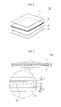
- FIG. 1 is an exploded perspective view showing a magnetic field shield sheet for a wireless charger according to the present invention
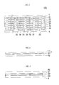
- FIG. 2 is a cross-sectional view showing an example of using one piece of nanocrystalline ribbon sheet according to a first embodiment of the present invention.
- a magnetic field shield sheet 10 for a wireless charger includes: at least one layer (or a multi-layer) thin magnetic sheet 2 separated and/or cracked into a plurality of fine pieces 20, by thermally treating an amorphous alloy ribbon or nanocrystalline alloy ribbon and then performing a flake treatment process; a protective film 1 that is adhered on an upper portion of the thin magnetic sheet 2; a double-sided tape 3 that is adhered on a lower portion of the thin magnetic sheet 2; and a release film 4 that is separably adhered on a lower portion of the double-sided tape 3.
- a thin ribbon made of an amorphous alloy or nanocrystalline alloy may be used as the thin magnetic sheet 2.
- a Fe-based or Co-based magnetic alloys may be used as the amorphous alloy, and considering the material cost, the Fe-based magnetic alloys are preferably used.
- Fe-Si-B alloys may be used as the Fe-based magnetic alloys.
- the content of Fe is 70-90 atomic% (which will be abbreviated as at%), and the content of a sum of Si and B is 10-30 at%.
- the content of Fe in the present invention is preferably 70-90 at%.
- the content of the sum of Si and B is in the range of 10-30 at%, an amorphous forming capability of an alloy is the most excellent.
- corrosion resistant elements such as Cr and Co can be added within 20 at% into this basic composition, and if necessary, other metallic elements may be included in small quantities in the basic composition to impart different properties.
- the Fe-Si-B alloys can be used; for example, the crystallization temperature of a certain Fe-Si-B alloy is 508°C, and the Curie temperature (Tc) thereof is 399°C.
- the crystallization temperature can be varied depending on the content of Si and B, or the other metal elements and the content thereof added in addition to ternary alloy elements.
- a Fe-based amorphous alloy for example, a Fe-Si-B-Co-based alloy may be used according to the required conditions, in the present invention.
- a thin ribbon made of a Fe-based nanocrystalline magnetic alloy can be used as the thin magnetic sheet 2.
- An alloy satisfying the following Equation 1 is preferably used as the Fe-based nanocrystalline magnetic alloy.
- an element A is at least one element selected from Cu and Au
- an element D is at least one element selected from Ti, Zr, Hf, V, Nb, Ta, Cr, Mo, W, Ni, Co, and rare earth elements
- an element E is at least one element selected from Mn, Al, Ga, Ge, In, Sn, and platinum group elements
- an element Z is at least one element selected from C, N, and P
- c, d, e, f, g, and h are numbers that satisfy the following relational expressions 0.01 ⁇ c ⁇ 8 at%, 0.01 ⁇ d ⁇ 10 at%, 0 ⁇ e ⁇ 10 at%, 10 ⁇ f ⁇ 25 at%, 3 ⁇ g ⁇ 12 at%, 15 ⁇ f + g + h ⁇ 35 at%, respectively, and the alloy structure of an area ratio of 20% or more is formed of the fine structure of the particle size of equal to or less than 50 nm.
- the element A is used to enhance corrosion resistance of the alloy, to prevent coarsening of crystal grains and at the same time, improve the magnetic properties such as the iron loss and the permeability of the alloy.
- the content of the element A is in the range from 0.01 to 8 at%.
- the element D is an element that is effective for the uniformity of the crystal grain diameter, the reduction of magnetostriction, etc. It is preferable that the content of the element D is in the range from 0.01 to 10 at%.
- the element E is an element that is effective for the soft magnetic properties of the alloy and improvement of corrosion resistance of the alloy.
- the content of the element E is preferably not more than 10 at%.
- the elements Si and B are elements that make the alloy to become amorphous at the time of producing the magnetic sheet. It is preferable that the content of the element Si is in the range from 10 to 25 at%, and it is preferable that the content of the element B is in the range from 3 to 12 at%.
- it may include the element Z as an element that makes the alloy to become amorphous, other than Si and B. In that case, the total content of the elements Si, B and Z is preferably in the range of 15 to 35 at%. It is preferable to implement the microcrystalline structure that crystal grains whose grain diameters are in the range of 5 to 30 nm exist in the range of 50 to 90% as an area ratio in the alloy structure.
- a Fe-Si-B-Cu-Nb alloy can be used as a Fe-based nanocrystalline magnetic alloy that is used in the thin magnetic sheet 2, and in this case, it is preferable that the content of Fe is 73-80 at%, the content of the sum of Si and B is 15-26 at%, and the content of the sum of Cu and Nb is 1-5 at%.
- An amorphous alloy that is obtained by producing such a composition range in the form of a ribbon can be easily precipitated into nanocrystalline grains by a thermal treatment to be described later.
- the protective film 1 may be implemented by using a resin film 11 including a polyethylene terephthalate (PET) film, a polyimide film, a polyester film, polyphenylene sulfade (PPS) film, a polypropylene (PP) film, or a fluorine resin-based film such as poly tetra fluoroethylene (PTFE), and is attached to one side of the thin magnetic sheet 2 through a first adhesive layer 12.
- a resin film 11 including a polyethylene terephthalate (PET) film, a polyimide film, a polyester film, polyphenylene sulfade (PPS) film, a polypropylene (PP) film, or a fluorine resin-based film such as poly tetra fluoroethylene (PTFE), and is attached to one side of the thin magnetic sheet 2 through a first adhesive layer 12.
- PET polyethylene terephthalate
- PPS polyphenylene sulfade
- PP polypropylene
- the protective film 1 is 1 to 100 um, in thickness, and it is preferably in the range of 10-30 ⁇ m, and it is more preferable to have a thickness of 20 ⁇ m.
- the protection film 1 used in the present invention 1 is attached on one side of the amorphous ribbon sheet that is used as the thin magnetic sheet 2, a release film 4a attached on the other surface of the first adhesive layer 12 to protect the first adhesive layer 12 is removed and then the protection film 1 is attached on one side of the amorphous ribbon sheet.
- the double-sided tape 3 is formed of a base member 32 made of a fluorine resin-based film, for example, a PET (Polyethylene Terephthalate) film, on both sides of which second and third adhesive layers 31 and 33 are formed.
- Release films 4 and 4b are attached on the outer surfaces of the second and third adhesive layers 31 and 33, respectively.
- the release films 4 and 4b are integrally formed in the manufacture of the double-sided tape 3, and are peeled off and removed when the magnetic field shield sheet 10, 10a, or 10b is attached on an electronic device.
- all release films 4 and 4b of FIG. 5 are removed from both sides of double-sided tapes 3a-3f interposed between the amorphous ribbon sheets 21-26.
- the double-sided tapes 3 and 3a-3f may be a type of including a base member as described above, but may be a type of including no base member but being formed of only adhesive layers. In the case of the double-sided tapes 3a-3f interposed between the amorphous ribbon sheets 21-26, it is preferable to use no-base type double-sided tapes in terms of a thinning process.
- the first to the third adhesive layers 12, 31, and 33 may be implemented by using, for example, acrylic adhesives, but may be of course possibly implemented by using different types of adhesives, as illustrated in FIG. 2 .
- the double-sided tapes 3 and 3a-3f may have 10, 20, 30 ⁇ m thick, preferably have a thickness of 10 ⁇ m.
- One piece of the thin magnetic sheet 2 that is used for the shield sheet 10, 10a or 10b may have a thickness of 15 to 35 ⁇ m for example.
- a thickness of the thin magnetic sheet 2 is preferably set to be in the range of 25 to 30 ⁇ m. The thinner the thickness of the ribbon may be, a breakage phenomenon of the ribbon may occur due to even a little shock at the time of performing a handling process after the heat treatment.
- a secondary coil (reception coil) 6 is attached to and used for a magnetic field shield sheet 10 as illustrated in FIGS. 16 and 17 , in the case of the magnetic field shield sheet 10.
- the secondary coil 6 forms a resonant circuit and therefore, the shield sheet 10 influences on inductance of the resonant circuit formed by the secondary coil (receiving coil) 6.
- the magnetic filed shield sheet 10 serves as an inductor that plays a role of shielding a magnetic field to block effects of a wireless power signal from a transmission device on the portable terminal 101 and simultaneously plays a role of guiding the wireless power signal to be received at the secondary coil of the reception device 6 in high efficiency.
- the thin magnetic sheet 2 is separated into a plurality of fine pieces 20 through a flake treatment process, and the plurality of fine pieces 20 have a size of several tens of micrometers ( ⁇ m) to equal to or less than three (3) mm.
- the heat generation problem of the battery can be blocked by reducing losses due to eddy currents.
- first and second adhesive layers 12 and 31 penetrate into gaps 20a of FIG. 10 between the plurality of fine pieces 20. Accordingly, the plurality of fine pieces 20 are isolated as adhesives that act as dielectrics.
- the fine pieces 20 are in contact with each other according to flow of the fine pieces 20, and thus the size of the fine pieces 20 increases to thereby cause a problem of increasing the eddy current losses, but block the problem from occurring, since the whole surface of the fine pieces 20 is surrounded by the dielectric, through the laminating process.
- a magnetic field shield sheet 10a for a wireless charger has a structure that one amorphous ribbon sheet 21 is used in which a protective film 1 is bonded on one side of the amorphous ribbon sheet 21, and a release film 4 is bonded via a double-sided tape 3 on the other side of the amorphous ribbon sheet 21.
- a magnetic field shield sheet 10b according to a second embodiment of the present invention as illustrated in FIG. 3 a number of amorphous ribbon sheets 21-26 are laminated and used as a thin magnetic sheet to increase the quality factor Q and the power transfer efficiency of the secondary coil 6.
- a permanent magnet to assist an alignment with the reception device can be adopted in the power transmission device in the wireless charger in order to enhance efficiency of the charger at maximum. That is, a circular permanent magnet is provided inside a primary coil (transmission coil) of the transmission device, and thus the exact alignment of the reception device overlying the transmission device is achieved to thereby hold the reception device to be stuck.
- the magnetic field shield sheet for a wireless charger is required to shield both alternating-current (AC) magnetic fields that are generated by the power transfer of a frequency of 100 KHz to 150 KHz from the transmission device, as well as direct-current (DC) magnetic fields that are generated by the permanent magnets.
- AC alternating-current
- DC direct-current
- the thin shield sheet is magnetically saturated to thereby cause problems of dropping a shielding performance as the shield sheet or sharply reducing power transmission efficiency.
- the permanent magnet is employed in the transmission device of the wireless charger, it is required to determine the amorphous ribbon sheets 21-26 to be laminated by taking into account a number of layers whose magnetic saturation is achieved by the permanent magnet.
- the Fe-based amorphous alloys are greater than the nanocrystalline alloys in view of the saturation field. Accordingly, in the case that amorphous ribbon sheets 21-26 made of the Fe-based amorphous alloys are used, 2 to 8 layers can be used by stacking one on another. For example, using 3 to 5 layers is preferably to obtain high magnetic permeability. In this case, the inductance of the laminate sheet (i.e., permeability) is preferably in the range of about 13 ⁇ H to 19 ⁇ H.
- the inductance of the laminate sheet is preferably in the range of about 13 ⁇ H to 21 ⁇ H.
- the inductance of the laminate sheet i.e., permeability
- the inductance of the laminate sheet is preferably in the range of about 13 ⁇ H to 21 ⁇ H.
- a number of amorphous ribbon sheets for example, six-layer amorphous ribbon sheets 21-26 are laminated and used as a thin magnetic sheet, and a number of adhesive layers or double-sided tapes 3a-3f are inserted between the amorphous ribbon sheets 21-26.
- the adhesive layers or double-sided tapes 3a-3f should be inserted and laminated between the amorphous ribbon sheets 21-26, so that gaps 20a between the fine pieces 20 are filled with the adhesive layers or double-sided tapes 3a-3f.
- the magnetic field shield sheets 10, 10a and 10b according to the present invention constitute a quadrangle such as a rectangular or square shape which usually corresponds to the battery cells, but constitute a polygonal shape such as a pentagon, or a circular or oval shape, and a combination of a rectangular shape and a circular shape partly.
- the magnetic field shield sheets have shapes corresponding to the shape of a region for which a magnetic field shielding action is required.
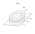
- the magnetic field shield sheet according to the present invention may be molded into an annular shape corresponding to a secondary coil of a reception device like a magnetic field shield sheet 10c shown in FIG. 6 according to a third embodiment of the present invention, to prevent a phenomenon that the magnetic field shield sheet is magnetized (or saturated) by a magnetic field of a permanent magnet, in the case that the permanent magnet is included at a central portion of a primary coil of a transmission device of a wireless charger.
- the magnetic field shield sheet 10c according to the third embodiment is made in any one of the correspondingly rectangular, circular, and elliptical shape, when the secondary coil is composed of any one of a rectangular, circular, and oval shape.
- the magnetic field shield sheet 10c is preferably made of a width by about 1-2 mm wider than that of the secondary coil 6.
- the magnetic field shield sheet 10c according to the third embodiment may have a structure that an annular thin magnetic sheet 2b on the upper surface of which an annular protective film 1a is attached is attached to a release film 4 through an annular double-sided tape 3.
- the annular magnetic field shield sheet 10c is preferably configured by using a release film 4 of a rectangular shape having an area larger than that of the annular magnetic field shield sheet 10c so as to be easily peeled off from the release film 4.
- an amorphous ribbon 2a (of FIG. 10 ) consisting of an amorphous alloy or nanocrystalline alloy is prepared by a rapidly solidification process (RSP) due to melt spinning (S11), and is cut in a predetermined length to then be laminated in a sheet form (S12) so that post- processing after a heat treatment can be easily performed.
- RSP rapidly solidification process
- S11 melt spinning
- S12 sheet form
- the amorphous ribbon 2a is an amorphous alloy
- an ultra-thin amorphous ribbon equal to or less than 30 ⁇ m made of a Fe-based amorphous ribbon, for example, a Fe-Si-B or Fe-Si-B-Co alloy is prepared by the rapidly solidification process (RSP) due to melt spinning, and then a laminated amorphous ribbon sheet is heat-treated under no magnetic circumstances for 30 minutes to 2 hours in a temperature range of 300°C to 600°C, so as to obtain a desired permeability (S13).
- the heat treatment is performed under an atmosphere of a temperature range at which oxidation is not generated even if the Fe content of the amorphous ribbon 2a is high, it is not necessary for the heat treatment to be done in an atmosphere furnace, but the heat treatment may proceed in air.
- the heat treatment is made under an oxidizing atmosphere or a nitrogen atmosphere, permeability of the amorphous ribbon has substantially no difference at the same temperature condition.
- the heat treatment temperature is less than 300°C
- the permeability higher than a desired permeability is obtained and it takes a longer time for the heat treatment.
- the permeability is significantly lowered by an overheat treatment, to thus fail to obtain a desired permeability.
- the heat treatment temperature is low, it takes a long time for the heat treatment.
- the heat treatment time is shortened.
- a Fe-based amorphous ribbon for example, an ultra-thin amorphous ribbon equal to or less than 30 ⁇ m made of a Fe-based amorphous ribbon, for example, a Fe-Si-B-Cu-Nb alloy is prepared by the rapidly solidification process (RSP) due to melt spinning, and then a laminated amorphous ribbon sheet is heat-treated under no magnetic circumstances for 30 minutes to 2 hours in a temperature range of 400°C to 700°C, so as to obtain a desired permeability (S13).
- RSP rapidly solidification process
- the Fe content of the amorphous ribbon 2a is equal to or more than 70 at%. Therefore, if the heat treatment is made in the air, the oxidation is generated and thus the heat treatment atmosphere is undesirable in terms of a visual appearance. Thus, it is preferable that the heat treatment should be performed in a nitrogen atmosphere. However, even if the heat treatment is made under an oxidizing atmosphere, permeability of the sheet has substantially no difference at the same temperature condition.
- the heat treatment temperature is less than 400°C, nanocrystalline particles are not sufficiently produced, and a desired permeability is not obtained. Further, it takes a longer time for the heat treatment. In addition, in the case of exceeding 700°C, the permeability is significantly lowered by an overheat treatment. When the heat treatment temperature is low, it preferably takes a long time for the heat treatment. In contrast, when the heat treatment temperature is high, the heat treatment time is preferably shortened.
- a thickness of the amorphous ribbons 2a of the present invention is in the range of 15 to 35 ⁇ m, and permeability of the amorphous ribbon 2a increases in proportion to the thickness of the ribbon.
- the amorphous ribbon is strong for embrittlement. Accordingly, when a flake treatment process is carried in a subsequent step, the flake treatment process can be easily made.
- a layer or a multi-layer of the amorphous ribbon 2a whose heat treatment has been made are used as many as a desired number of layers, and then a flake treatment process is performed in a state where a double-sided tape 3 is attached (S14) in which the protective film 1 is attached to one side of double-sided tape 3 and the release film 4 is attached to the other side of the double-sided tape 3.
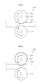
- the flake treatment process is performed to make a laminate sheet 100 where the protective film 1, the amorphous ribbon 2a, the double-sided tape 3, and the release film 4 are sequentially stacked, passed through first and second flake devices 110 and 120, for example, as shown in FIGS. 8 and 9 , to thereby allow the amorphous ribbon 2a to be separated into a number of fine pieces 20.
- the separated fine pieces 20 maintain a state of being separated by first and second adhesive layers 12 and 31 bonded to both side surfaces of the amorphous ribbon 2a.
- an available flake device 110 may consist of a metal roller 112 on the outer surface of which a plurality of irregularities 116 are formed, and a rubber roller 114 that is disposed in opposition to the metal roller 112.
- a second flake device 120 may be composed of a metal roller 122 on the outer surface of which a plurality of spherical balls 126 are mounted, and a rubber roller 124 that is disposed in opposition to the metal roller 122.
- the amorphous ribbon 2a is separated into the fine pieces 20 and gaps 20a are formed between the fine pieces 20, as shown in FIG. 10 .
- the fine pieces 20 of the amorphous ribbon 2a are formed to have a size of a range of several tens micrometers ( ⁇ m) to 3 milimeters (mm), a reverse magnetic field is made to increase to thereby remove a hysteresis loss and to thus heighten a uniformity of the permeability of the sheet.
- the flake treatment process of the amorphous ribbon 2a may reduce the surface area of the fine pieces 20 and prevent a heat generation problem caused by an eddy current that is produced by an alternating-current magnetic field.
- the flake treated laminate sheet 200 has the gaps 20a between fine pieces 20.
- the amorphous ribbon is oxidized and the appearance of the amorphous ribbon is poor and the shield performance is degraded.
- the fine pieces 20 are in contact with each other along the flow of the fine pieces 20, to accordingly increase the size of the fine pieces 20 and to thus cause a problem that the eddy-current loss increases.
- the flake treated laminate sheet 200 may have non-uniformity caused on the surface of the sheet during performing the flake treatment process, and stabilization of the flake treated ribbon is needed.
- the flake treated laminate sheet 200 undergoes a laminating process for flattening, slimming, and stabilization of the sheet 200, while simultaneously filling the adhesive into the gaps 20a of the fine pieces 20 (S15).
- the adhesive is filled into the gaps 20a of the fine pieces 20 (S15).
- a laminating device 400 for the laminating process may employ a roll press type including a first pressing roller 210 and a second pressing roller 220 that is disposed at a predetermined distance from the first pressing roller 210, between which the flake treated laminate sheet 200 passes.
- a laminating device 500 for the laminating process may employ a hydraulic press type including a lower pressing member 240 and an upper pressing member 250 that is vertically movably disposed on the upper side of the lower pressing member 240.
- the flake treated laminate sheet 200 When the flake treated laminate sheet 200 is heated at room temperature or at a temperature of 50°C to 80°C, and then is passed through the laminating device 400 or 500, a first adhesive layer 12 of the protective film 1 is pressed, while some of the adhesive of the first adhesive layer 12 are introduced into the gaps 20a to seal the gaps 20a. Simultaneously, the double-sided tape 3 is pressed, while some of the adhesive of the second adhesive layer 31 are introduced into the gaps 20a to seal the gaps 20a.
- the first adhesive layer 12 and the second adhesive layer 31 may be formed by using an adhesive that can be deformed at the time of being pressed at room temperature, or may be formed by using a thermoplastic adhesive that can be thermally deformed by applied heat.
- first adhesive layer 12 and the second adhesive layer 31 preferably have a thickness of at least 50% when compared to the thickness of the amorphous ribbon so as to sufficiently fill the gaps 20a between the fine pieces 20.
- the interval between the first pressure roller 210 and the second pressure roller 220 and the interval between the upper pressing member 250 and the lower pressing member 240 when the upper pressing member 250 is in a lowered state are preferably formed of a thickness of 50% or less when compared to the thickness of the laminate sheet 200, so that the adhesive of the first adhesive layer 12 and the second adhesive layer 31 can be introduced into the gaps 20a.
- Any device of performing the pressing of the laminate sheets 100 and 200 and the flake treatment process, can be used in the present invention.
- an electromagnetic wave absorbing sheet 10 may have a structure that the first adhesive layer 12 and the second adhesive layer 31 partially fill the gaps 20a between the fine pieces 20 at a state where the amorphous ribbon 2a is separated into the fine pieces 20, to thereby prevent the oxidation and the flow of the amorphous ribbon 2a.
- the magnetic field shield sheet 10 having undergone the laminating process is stamped into the size and shape necessary for place and use for electronic devices so as to be produced into products (S16).
- a thickness of the magnetic filed shield sheet 10b including the protective film 1 and the release film 4 is 212 ⁇ m before the laminating process is performed, but the former is 200 ⁇ m after laminating process is performed.
- a temporary protective film for protecting the protective film 1 is attached on top of the protective film 1 before performing a treatment process, and then the temporary protective film on the surface of the magnetic sheet 2 is peeled off and removed after completion of the treatment process.
- a humidity test was conducted for 120 hours at temperature of 85°C and humidity of 85% with respect to the magnetic field shield sheet 10 obtained in accordance with the invention and the laminate sheet 200 that has undergone the flake process but does not pass through the lamination process.
- the magnetic field shield sheet according to the present invention may be configured by using dissimilar materials illustrated in FIGS. 15a and 15b as a thin film magnetic sheet.
- a thin film magnetic sheet 35 can be configured in a hybrid form in which a bonding layer 35c is inserted and combined between a first magnetic sheet 35a of a high permeability and a second magnetic sheet 35b of a permeability lower than that of the first magnetic sheet 35a.
- An amorphous ribbon sheet consisting of the above-described amorphous alloy or nanocrystalline alloy, a permalloy sheet having an excellent soft magnetic characteristic, or a MPP (Moly Permalloy Powder) sheet can be used as the first magnetic sheet 35a.
- the second magnetic sheet 35b may be formed of a polymer sheet consisting of a magnetic powder of a high permeability such as an amorphous alloy powder, soft magnetic powder, or a sendust, and a resin.
- the amorphous alloy powder has a composition selected from the group consisting of for example, Fe-Si-B, Fe-Si-B-Cu-Nb, Fe-Zr-B and Co-Fe-Si-B, and preferably is formed of an amorphous alloy powder comprising one or more amorphous alloys.
- the hybrid-type thin film magnetic sheet 35 is formed by using an amorphous ribbon sheet and a ferrite sheet with low frequency dependence that are laminated and stacked one over another, as the first and second magnetic sheets 35a and 35b, as shown in FIG. 15A . Accordingly, it is possible to solve both the near field communications (NFC) function and the wireless charging function by using the ferrite sheet for the magnetic field shield for the NFC and by using the amorphous ribbon sheet for the wireless charger.
- the hybrid-type thin film magnetic sheet 35 may be formed by using a certain area of an amorphous ribbon sheet at a center of the hybrid-type thin film magnetic sheet 35, as a first magnetic sheet 35a, and by combining a second annular magnetic sheet 35b that surrounds the whole of the first magnetic sheet 35a on the outside of the first magnetic sheet 35a into a ferrite loop, as shown in FIG. 15B . That is, the ferrite having a relatively smaller permeability than the amorphous sheet is formed in a loop form and is arranged in the outer block of the amorphous sheet.
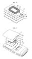
- FIG. 16 is an exploded perspective view showing a structure that a magnetic field shield sheet according to the present invention is applied to a reception device for a wireless charger
- FIG. 17 is an exploded perspective view showing that the reception device for a wireless charger of FIG. 16 is assembled with a battery cover and coupled with a portable terminal.
- a receiving-side secondary coil 6 of the wireless charger is attached on an upper portion of a protective film of a magnetic field shield sheet 10 by using a double-sided tape 30b.
- a finishing material (not shown) is adhered to an adhesive layer 33 of the double-sided tape 30b that is exposed by removing the release film 4 from the lower portion of the magnetic field shield sheet 10, for example, as shown in FIG. 13 .
- an assembly of the secondary coil 6 and the magnetic field shield sheet 10 is attached to a battery cover 5 for a portable terminal device 101 by using a double-sided tape 30a. Then, when the battery cover 5 is coupled to the mobile terminal device 101, the magnetic field shield sheet 10 is used in the form of a cover of the battery 7.
- An assembly position of the magnetic field shield sheet 10 may be disposed in the outside of the battery, or may be disposed in a well-known method.
- the secondary coil 6 having a well-known structure may be also used.
- the secondary coil 6 may be configured to have a spiral coil 6a made of any one of a rectangular, round, oval shape on a substrate made of a synthetic resin 6b such as a polyimide (PI), as shown in FIG. 16 .
- PI polyimide
- the secondary coil 6 may be assembled into a thin film structure by directly forming the spiral coil 6a on a single adhesive sheet that serves as an insulating layer in place of the synthetic resin substrate 6b and the double-sided tape 30b, for example, a double-sided tape in a transfer manner.
- the spiral coil 6a that plays a role of receiving power wirelessly may be also formed by winding a general coil in the form of a planar inductor to then be adhered on a substrate.
- the portable mobile terminal device 101 includes a rectifier (not shown) that rectifies an AC voltage generated in the spiral coil 6a of the secondary coil 6 into a direct-current (DC) voltage in the inside of a main body, in which the rectified DC voltage is charged into a battery (i.e., a secondary cell 7).
- a rectifier not shown
- DC direct-current
- the magnetic field shield sheet 10 includes a multi-layer magnetic sheet 2 that is flake treated and separated into a plurality of fine pieces 20, to thereby increase a quality factor (Q), and to thus increase electric power transmission efficiency.
- the magnetic field shield sheet 10 is flake treatment processed, to thereby reduce a surface area of the ribbon and to accordingly prevent a heat generation problem caused by the eddy currents generated by the AC magnetic field.
- the magnetic flux generated from the primary coil of the transmission device is blocked from being interlinked with a circuit board of the portable terminal device and the battery (or a secondary battery) 7 to thus suppress heat generation.
- FIG. 18 is a plan view showing a dual-antenna structure in which an antenna for near field communications (NFC) and an antenna for a wireless charger are integrally formed by using a flexible printed circuit board (FPCB).
- NFC near field communications
- FPCB flexible printed circuit board
- a dual antenna 40 that performs both the NFC function and the wireless charging function is preferably implemented by using a flexible printed circuit board (FPCB) having a double-sided substrate structure.
- FPCB flexible printed circuit board
- the dual antenna according to the present invention is not limited thereto, but a different type of an antenna structure may be used.
- a dual antenna 40 is configured to include, for example, a NFC antenna coil 41 and a wireless charger antenna coil 43 that are formed together on a substrate 49.
- the substrate 49 may be configured by using, for example, a double-sided adhesive tape, and the NFC antenna coil 41 and the wireless charger antenna coil 43 are formed on the adhesive substrate 49 by using a transfer method.
- the NFC antenna coil 41 Since the NFC antenna coil 41 has a higher frequency band than the wireless charger antenna coil 43, the NFC antenna coil 41 is formed to have a conductive pattern of a rectangular shape of a fine line width along the outside of the substrate 49. In addition, since the wireless charger antenna coil 43 requires the power transmission and uses a lower frequency band than the NFC antenna coil 41, the wireless charger antenna coil 43 is formed in the inside of the NFC antenna coil 41 to have a conductive pattern of a substantially elliptical shape of a line width wider than the width of the NFC antenna coil 41.
- the dual antenna 40 is configured to have a pair of terminal strips 41a and 41b, and 43a and 43b, which are disposed on a projection of the substrate 49 respectively extended at one side of the NFC antenna coil 41 and the wireless charger antenna coil 43.
- the outer line of the NFC antenna coil 41 is directly connected to a first terminal block 41a, and the inner line thereof is connected to a second terminal block 41b via a terminal connecting pattern (not shown) that is formed on the rear surface of the substrate 49 through conductive throughholes 45a and 45b.
- the outer line of the wireless charger antenna coil 43 is connected to a third terminal block 43a via a terminal connecting pattern (not shown) that is formed on the rear surface of the adhesive substrate 49 through conductive throughholes 47a and 47b, and the inner line thereof is connected to a fourth terminal block 43b via a terminal connecting pattern (not shown) that is formed on the rear surface of the substrate 49 through conductive throughholes 47c and 47d.
- a protective film for protecting an antenna coil pattern such as, for example, PSR (Photo Solder Resist) is preferably formed on the surface of the substrate 49.
- a shield sheet employing a hybrid type magnetic sheet of FIGS. 15A and 15B may be used.
- Example 1 A magnetic field shield sheet using one amorphous ribbon sheet that was not heat treated (Comparative Example 2), a magnetic field shield sheet using one nanocrystalline ribbon sheet that was heat treated (Comparative Example 3), a magnetic field shield sheet using one nanocrystalline ribbon sheet that was heat treated and flake treated (Example 1), a magnetic field shield sheet using two nanocrystalline ribbon sheets that were heat treated and flake treated (Example 2), a magnetic field shield sheet using three nanocrystalline ribbon sheets that were heat treated and flake treated (Example 3), and a magnetic field shield sheet using four nanocrystalline ribbon sheets that were heat treated and flake treated (Example 3), were prepared respectively.
- An amorphous alloy ribbon sheet applied for a shield sheet was prepared by comprising: making an amorphous ribbon made of a Fe 73.5 Cu 1 Nb 3 Si 13.5 B 9 alloy in a thickness of 25 ⁇ m by a rapid solidification method (RSP) due to melt spinning; cutting the amorphous ribbon in a sheet form and heat treating the cut sheet at 580°C, under no magnetic field, in a nitrogen (N 2 ) atmosphere, for 1 hour, to thereby obtain the amorphous ribbon sheet; inserting the amorphous ribbon sheet between a protective film of 10 ⁇ m thick using a polyethylene terephthalate (PET) base member and a double-sided tape (with a release film excluded) of 10 ⁇ m thick using a PET base member, to thereby prepare a laminate sheet; and performing flake treatment and lamination treatment processes respectively by using a flake treatment processing device of FIG. 8 and a laminating device of FIG. 11 .
- RSP rapid solidification method
- a circular planar coil having an inductance of 12.2 ⁇ H and a resistance of 237 m ⁇ was used as a secondary coil bonded to the shield sheet, that is, as a measuring coil. Then, the measuring coil was connected to an LCR meter to measure the inductance (L), capacitance (C), and resistance (R), and then the LCR meter was located on the shield sheet. Then, a certain pressure was applied to the measuring coil by placing a rectangular parallelepiped having a weight of about 500 g on the measuring coil, and setting values of the LCR meter were set to be 100 kHz and 1 V.
- the inductance (Ls) and the coil quality factor (Q) of the secondary coil is increased, and the magnetoresistance (Rs) is decreased. Accordingly, a transmission efficiency of the magnetic flux transmitted from the transmission device for the secondary coil for the wireless charger can be increased.
- the magnetic field shield sheets of Examples 5 to 7 were prepared into a rectangular shape in the same manner as in Examples 1 to 4. However, the number of nanocrystalline ribbon sheets laminated in the magnetic field shield sheets was changed into 6, 9, or 12.
- the magnetic field shield sheet of Example 8 was different from that of Example 6, in a point that the former was configured by making the shape of the latter (the number of nanocrystalline ribbon sheets was six) in the same annular shape as that of the secondary coil.
- Comparative Example 1 in the case that no magnetic field shield sheet is used
- magnetic field shield sheets of Examples 5 to 8, respectively as shown in FIG. 19
- a separator sheet of paper 9 of 0.5 mm thick was placed on the upper portion of the transmission device 8 of the wireless charger, and then the magnetic field shield sheet 10 and the reception device with which the secondary coil 6 was assembled were placed on a lithium ion battery 7.
- voltage (V) and current (mA) applied to the primary coil of the transmission device 8 and voltage (V) and current (mA) applied to the secondary coil 6 of the reception device were measured and shown in the following Table 2, based on which the power transmission efficiency was calculated.
- a thickness of a shield sheet using a ferrite sheet due to a DC magnetic field of the permanent magnet should have been at least 0.5 T in order to perform an optimum wireless charging operation.
- Example 7 of the present invention permeability is high, and thus similar properties to the ferrite or the polymer sheet were obtained even at a thickness of 0.3 T lower than 0.5 T which was exhibited in the case of the conventional shield sheet using a ferrite sheet.
- the magnetic field shield sheet according to Example 8 was set as shown in FIG. 19 , and temperatures of the battery and the nanocrystalline ribbon sheet of the magnetic field shield sheet were measured in units of an interval of 30 minutes for the charging time from 30 minutes to 4 hours 30 minutes, and the results were shown in Table 3.
- Table 3 Charging time interval Temperature of battery (°C) Temperature of ribbon sheet (°C) 0.5 hours 29.5 30 1.0 hour 30 30 1.5 hours 30.5 30.5 2.0 hours 30.5 30.5 2.5 hours 30.5 31 3.0 hours 30.5 31 3.5 hours 30.5 31 4.0 hours 30.5 31 4.5 hours 30.5 31
- An amorphous alloy ribbon sheet applied for a shield sheet was prepared by comprising: making an amorphous ribbon made of a Fe 67 B 14 Si 1 Co 18 alloy in a thickness of 25 ⁇ m by a rapid solidification method (RSP) due to melt spinning; cutting the amorphous ribbon in a sheet form and heat treating the cut sheet at 487°C, 459°C, and 450°C, under no magnetic field, for 1 hour, respectively, to thereby obtain the amorphous ribbon sheet; inserting the amorphous ribbon sheet between a protective film of 10 ⁇ m thick using a polyethylene terephthalate (PET) base member and a double-sided tape (with a release film excluded) of 10 ⁇ m thick using a PET base member, to thereby prepare a laminate sheet; and performing flake treatment and lamination treatment processes respectively by using a flake treatment processing device of FIG. 8 and a laminating device of FIG. 11 .
- RSP rapid solidification method
- the charging efficiency for the inductance of each sheet was the highest in the case that the inductance (permeability) of the sheet that was heat treated at 459°C was 15 ⁇ H. As the number of laminated amorphous ribbon sheets was increased from one to eight, the charging efficiency was also increased proportionally with the number of the sheets. In the case that about 4 sheets were laminated, a saturation phenomenon occurred, and in the case of exceeding eight sheets, the charging efficiency was decreased.
- the maximum charging efficiency of the laminated sheets for the number of laminated sheets was measured by using the amorphous ribbon sheet of the inductance (permeability) of 15 ⁇ H, and the results were shown in Table 5.
- the maximum charging efficiency was obtained in the state where value of a time constant of the reception device was adjusted to make the efficiency set to a maximum value based on value of the inductance of the reception device of the wireless charger, that is, the secondary coil.
- Table 5 Permeability Maximum charging efficiency (%) 1 sheet 2 sheets 3 sheets 4 sheets 15 ⁇ H 61.3 68.7 71.1 71.9
- the efficiency was increased according to the number of laminated amorphous ribbon sheets, and the maximum charging efficiency was 71.9 % in the highest in the case of four sheets.
- the present invention greatly reduces a loss due to eddy currents by a flake treatment process of an amorphous ribbon, to thereby block an effect of a magnetic field influencing upon a main body and a battery of a portable mobile terminal device and simultaneously to increase a quality factor (Q) of a secondary coil, and to thus exhibit excellent electric power transmission efficiency.
- the present invention fills a gap between fine pieces of an amorphous ribbon through a flake treatment process of the amorphous ribbon and then a compression laminating process with an adhesive, to thereby prevent water penetration, and simultaneously surrounds all surfaces of the fine pieces with an adhesive (or a dielectric) to thus mutually isolate the fine pieces to thereby promote reduction of eddy currents and prevent shielding performance from falling.
- the present invention establishes a shape of a shield sheet into a shape similar to that of a coil of a receiving device for a wireless charger, to thereby exhibit a high power transmission efficiency or equal power transmission efficiency while lowering thickness of the magnetic field shield sheet to be equal to or less than 0.3 mm, even though a small number of nanocrystalline ribbons are used.
- the present invention sequentially performs a flake treatment process and a laminating process by using a roll-to-roll method, to thereby achieve a sheet molding process to thus maintain original thickness of the sheet and to thus exhibit high productivity and inexpensive manufacturing costs.
- a magnetic field shield sheet for a wireless charger may be applied to a variety of portable electronic devices including a portable terminal device, to thereby block an influence upon the portable terminal device by AC and DC magnetic fields that are generated when a wireless charging function is implemented in a non-contact (wireless) manner, and to thereby assist the magnetic field shield sheet for a wireless charger to absorb electromagnetic waves necessary for the wireless charging function.
Landscapes
- Engineering & Computer Science (AREA)
- Power Engineering (AREA)
- Computer Networks & Wireless Communication (AREA)
- Physics & Mathematics (AREA)
- Electromagnetism (AREA)
- Microelectronics & Electronic Packaging (AREA)
- Signal Processing (AREA)
- Shielding Devices Or Components To Electric Or Magnetic Fields (AREA)
- Charge And Discharge Circuits For Batteries Or The Like (AREA)
- Soft Magnetic Materials (AREA)
- Regulation Of General Use Transformers (AREA)
Abstract
Description
- The present invention relates to a magnetic field shield sheet for a wireless charger, a method of manufacturing the magnetic field shield sheet, and a receiver for the wireless charger by using the magnetic field shield sheet, and more particularly to a magnetic field shield sheet for a wireless charger, which blocks an effect of an alternating-current magnetic field generated when a charger function for a portable mobile terminal device is implemented in a non-contact wireless manner on a main body of the portable mobile terminal device and exhibits excellent electric power transmission efficiency, a method of manufacturing the magnetic field shield sheet, and a receiver for the wireless charger by using the magnetic field shield sheet.
- As methods of charging secondary batteries mounted in electronic equipment such as portable terminals and video cameras, there are two types of charging methods, i.e., a contact type charging method and a non-contact type charging method. The contact type charging method carries out a charging operation by making an electrode of a power reception device in direct contact with an electrode of a power feeding device.
- The contact type charging method is commonly used in a wide range of applications, since a structure of a device implementing the contact type charging method is simple. However, in association with miniaturization and weight reduction of electronic equipment, various electronic devices become light in the weight thereof, and accordingly a low contact pressure between electrodes of the power reception device and the power feeding device may cause problems such as charge failure charge error. Further, secondary batteries are weak at heat, which needs to prevent the temperature rise of the batteries, and to pay attention to a circuit design so as not to cause overcharge and overdischarge. To cope with these problems, a non-contact type charging method is being considered in recent years.
- The non-contact type charging method is a charging method using an electromagnetic induction principle in which coils are mounted at both sides of the power reception device and the power feeding device.
- A non-contact type charger can be miniaturized by putting a ferrite core to be in a magnetic core and winding coils around the ferrite core. Furthermore, for miniaturization and reduction in thickness, a technique of forming a resin substrate by mixing ferrite powder and amorphous powder and mounting a coil and the like on the resin substrate, has been proposed. However, in the case that a ferrite sheet is processed thinly, the thinly processed ferrite sheet may be easily broken and weak in impact resistance. As a result, there have been problems that defects have occurred in the power reception device due to a fall or collision of the non-contact type charger.
- Further, in order to reduce the thickness of a power reception portion of an electronic device in response to reduction in the thickness of the electronic device, a planar coil that is formed by printing a metal powder paste as a coil has been employed. A structure of strengthening a coupling of a planar coil and a magnetic sheet has been proposed. In the proposed structure, a magnetic body or a magnetic sheet is used as a core material to strengthen the coupling between primary and secondary coils.
- Meanwhile, if a power transmission speed increases, defects between adjacent transformers, as well as defects caused by heat from the surrounding components, may be likely to occur. That is, in the case that the planar coils are used, the magnetic flux passing through the planar coils is connected to a substrate or the like inside an electronic device, an internal portion of the electronic device may be heated due to eddy currents caused by electromagnetic induction. As a result, large power cannot be transmitted and thus a time-consuming problem may be caused for charging the electronic device.
- To cope with this problem, a magnetic body or a magnetic sheet was used as a shielding member on the back of the substrate. In order to obtain a sufficient shielding effect, as the magnetic body or the magnetic sheet may have the larger magnetic permeability, and the larger area and thickness, a more effective shielding effect can be obtained.
- In general, a magnetic body such as an amorphous ribbon, a ferrite sheet, or a polymer sheet containing magnetic powder is used as the magnetic field shield sheet. An effect of focusing a magnetic field for improving magnetic field shielding performance and additional features may be good in the order of amorphous ribbons, a ferrite sheet, and a polymer sheet containing magnetic powder, with high magnetic permeability.
- In the case of a power reception device of a conventional non-contact type charging system, a magnetic body or a magnetic sheet with high magnetic permeability and large volume is disposed on the opposite surface to a primary coil side, i.e., on the surface of a secondary coil, for reinforcement of a coupling for improving transmission efficiency, and for improving a shielding performance for suppression of heat generation. According to this arrangement, fluctuations in the inductance of the primary coil become large, and an operation condition of a resonant circuit is shifted from a resonance condition at which a sufficient effect can be exhibited according to a relative positional relationship between the magnetic body and the primary coil.
- Korean Patent Application Publication No.
10-2010-31139 - In other words, according to Korean Patent Application Publication No.
10-2010-31139 - The composite magnetic body is set so that the first magnetoresistance of a first magnetic sheet adjacent to the spiral coil is less than or equal to 60, the second magnetoresistance of a second magnetic sheet laminated on the first magnetic sheet is greater than or equal to 100, and a value of the second magnetoresistance divided by the first magnetoresistance is equal to or greater than 1.0.
- The first magnetic sheet is prepared by bonding polycarbonate resins on both surfaces of a first amorphous ribbon by using adhesive layers, respectively, and the second magnetic sheet is prepared by bonding polycarbonate resins on both surfaces of a second amorphous ribbon with large relative permeability by using adhesive layers, respectively. Then, the first magnetic sheet and the second magnetic sheet are integrally bonded via an adhesive layer.
- Meanwhile, the ferrite sheet or a polymer sheet containing magnetic powder has the magnetic permeability a little lower than the amorphous ribbon, and thus in order to improve the performance of such low magnetic permeability, thickness of the ferrite sheet or a polymer sheet becomes large compared to the thin amorphous ribbon of several tens µm. Therefore, it is difficult to respond to a thinning tendency of terminals.
- Further, in the case of an amorphous ribbon with high magnetic permeability, the ribbon itself is a metal thin plate, and thus there is no burden on thickness of the amorphous ribbon. However, when an alternating-current magnetic field according to a frequency of 100 kHz used for power transmission is applied to the amorphous ribbon, the functionality of applications may be reduced due to an influence of eddy currents of the ribbon surface, or problems of reducing wireless charging efficiency and causing heat generation may occur.
- Co-based or Fe-based amorphous ribbons can increase surface resistance slightly, through heat treatment. However, in the case that a processing treatment such as a flake treatment process of reducing a surface area of the ribbon is performed in order to further reduce the eddy current effects, the magnetic permeability is significantly degraded and the function as the shield sheet is greatly degraded.
- Also, most of wireless chargers employ a structure of adopting permanent magnets that assist an alignment with a power receiver in a power transmitter for power transmission, in order to increase the power transfer efficiency of the chargers to the maximum. A magnetization or saturation phenomenon occurs in a thin shield sheet due to a direct-current magnetic field of the permanent magnets, to thereby decrease the performance of the chargers or sharply decreasing the power transmission efficiency.
- Accordingly, in the case of the conventional chargers, the thickness of the shield sheet must be quite thick in the order of 0.5T or higher, in order to indicate shielding features without being affected by the permanent magnets, and to maintain high power transmission efficiency, which may cause a major obstacle on slimming of portable terminals.
- A voltage induced in a secondary coil of a wireless charger is determined by the Fara-day's law and the Lenz's law, and thus it is more advantageous to have the greater amount of magnetic flux linked with the secondary coil in order to obtain a high voltage signal. The amount of the magnetic flux becomes large as the amount of a soft magnetic material contained in the secondary coil becomes large and the magnetic permeability of the material becomes high. In particular, since the wireless chargers essentially employ a non-contact power transmission system, a magnetic field shield sheet in which the secondary coil is mounted is needed to be made of a magnetic material with high permeability, in order to focus wireless electromagnetic waves made from the primary coil of a power transmission device, on the secondary coil of a power reception device.
- Conventional magnetic field shield sheets for wireless chargers do not present solutions for attaining the thin film but solving the heat generation problem due to shields and improving the wireless charging efficiency. Thus, the present inventors recognized that inductance (magnetic permeability) is less reduced and magnetoresistance is greatly reduced, although an amorphous ribbon undergoes flakes in the case of the amorphous ribbon, and thus a quality factor (Q) of the secondary coil is increased, to thereby reach the present invention.
- To solve the above problems or defects, it is an object of the present invention to provide a magnetic field shield sheet for a wireless charger, which greatly reduces a loss due to eddy currents by a flake treatment process of an amorphous ribbon, to thereby block an effect of a magnetic field influencing upon a main body and a battery of a portable mobile terminal device and simultaneously to increase a quality factor (Q) of a secondary coil, and to thus exhibit excellent electric power transmission efficiency, a method of manufacturing the magnetic field shield sheet, and a receiver for the wireless charger by using the magnetic field shield sheet.
- It is another object of the present invention to provide a magnetic field shield sheet for a wireless charger, which fills a gap between fine pieces of an amorphous ribbon through a flake treatment process of the amorphous ribbon and then a compression laminating process with an adhesive, to thereby prevent water penetration, and which simultaneously surrounds all surfaces of the fine pieces with an adhesive (or a dielectric) to thus mutually isolate the fine pieces to thereby promote reduction of eddy currents and prevent shielding performance from falling, and a manufacturing method thereof.
- It is still another object of the present invention to provide a magnetic field shield sheet for a wireless charger, which establishes a shape of a shield sheet into a shape similar to that of a secondary coil of a receiving device for a wireless charger, to thereby exhibit high power transmission efficiency even though a small number of nanocrystalline ribbons are used, and a power reception device using the magnetic field shield sheet.
- It is yet another object of the present invention to provide a magnetic field shield sheet for a wireless charger, which sequentially performs a flake treatment process and a laminating process by using a roll-to-roll method, to thereby achieve a sheet molding process to thus maintain original thickness of the sheet and to thus exhibit high productivity and inexpensive manufacturing costs.
- To accomplish the above and other objects of the present invention, according to an aspect of the present invention, there is provided a magnetic field shield sheet for a wireless charger, the magnetic field shield sheet comprising:
- at least one layer thin magnetic sheet made of an amorphous ribbon separated into a plurality of fine pieces;
- a protective film that is adhered on one surface of the thin magnetic sheet via a first adhesive layer provided on one side of the protective film; and
- a double-sided tape that is adhered on the other surface of the thin magnetic sheet via a second adhesive layer provided on one side of the double-sided adhesive tape,
- wherein gaps among the plurality of fine pieces are filled by some parts of the first and second adhesive layers, to thereby isolate the plurality of fine pieces.
- According to another aspect of the present invention, there is provided a method of manufacturing a magnetic field shield sheet for a wireless charger, the method comprising the steps of:
- adhering a protective film and a double-sided tape formed of a release film on an exposed surface of the double-sided tape, on both sides of at least one layer thin magnetic sheet made of an amorphous ribbon, to thereby form a laminate sheet;
- performing a flake treatment process of the laminate sheet to thus separate the thin magnetic sheet into a plurality of fine pieces; and
- laminating the flake treated laminate sheet, to thus fill some parts of first and second adhesive layers provided in the protective film and the double-sided tape into gaps among the plurality of fine pieces,
- a protective film that is adhered on one surface of the thin magnetic sheet via a first adhesive layer provided on one side of the protective film; and
- a double-sided tape that is adhered on the other surface of the thin magnetic sheet via a second adhesive layer provided on one side of the double-sided adhesive tape, together with flattening and thinning of the laminate sheet, and to thereby isolate the plurality of fine pieces.
- According to still another aspect of the present invention, there is provided a reception device for a wireless charger that charges a secondary battery by an electromagnetic induction method from a transmission device for the wireless charger, the reception device comprising:
- a secondary coil that receives a wireless high frequency signal transmitted by the electromagnetic induction method from the transmission device; and
- a magnetic field shield sheet that is disposed between the secondary coil and the secondary battery, and that shields a magnetic field generated by the wireless high frequency signal and simultaneously induces the secondary coil to absorb the wireless high frequency signal necessary to perform a wireless charging function,
- wherein the magnetic field shield sheet comprises:
- at least one layer thin magnetic sheet made of an amorphous ribbon separated into a plurality of fine pieces;
- a protective film that is adhered on one surface of the thin magnetic sheet via a first adhesive layer provided on one side of the protective film; and
- a double-sided tape that is adhered on the other surface of the thin magnetic sheet via a second adhesive layer provided on one side of the double-sided adhesive tape, wherein gaps among the plurality of fine pieces are filled by some parts of the first and second adhesive layers, to thereby isolate the plurality of fine pieces.
- As described above, the present invention provides a magnetic field shield sheet for a wireless charger, which greatly reduces a loss due to eddy currents by a flake treatment process of an amorphous ribbon, to thereby block an effect of a magnetic field influencing upon a main body and a battery of a portable mobile terminal device and simultaneously to increase a quality factor (Q) of a secondary coil, and to thus exhibit excellent electric power transmission efficiency, a method of manufacturing the magnetic field shield sheet, and a receiver for the wireless charger by using the magnetic field shield sheet.
- In addition, the present invention provides a magnetic field shield sheet for a wireless charger, which fills a gap between fine pieces of an amorphous ribbon through a flake treatment process of the amorphous ribbon and then a compression laminating process with an adhesive, to thereby prevent water penetration, and which simultaneously surrounds all surfaces of the fine pieces with an adhesive (or a dielectric) to thus mutually isolate the fine pieces to thereby promote reduction of eddy currents and prevent shielding performance from falling, and a manufacturing method thereof. As a result, all surfaces of the fine pieces are surrounded by an adhesive (or a dielectric material) to thereby prevent water from penetrating into the amorphous ribbon and to thus prevent the amorphous ribbon from being oxidized and changes in appearance and characteristics from being deteriorated.
- Moreover, the present invention provides a magnetic field shield sheet for a wireless charger, which establishes a shape of a shield sheet into a shape similar to that of a coil of a receiving device for a wireless charger, to thereby exhibit a high power transmission efficiency or equal power transmission efficiency while lowering thickness of the magnetic field shield sheet to be equal to or less than 0.3 mm, even though a small number of nanocrystalline ribbons are used, and a power reception device using the magnetic field shield sheet.
- In addition, the present invention provides a magnetic field shield sheet for a wireless charger, which sequentially performs a flake treatment process and a laminating process by using a roll-to-roll method, to thereby achieve a sheet molding process to thus maintain original thickness of the sheet and to thus exhibit high productivity and inexpensive manufacturing costs.
-
-
FIG. 1 is an exploded perspective view showing a magnetic field shield sheet for a wireless charger according to the present invention. -
FIG. 2 is a cross-sectional view showing an example of using one piece of nanocrystalline ribbon sheet according to a first embodiment of the present invention. -
FIG. 3 is a cross-sectional view showing an example of using six pieces of nanocrystalline ribbon sheets according to a second embodiment of the present invention. -
FIGS. 4 and 5 are cross-sectional views showing the structure of a protective film and a double-sided tape that are respectively used in the present invention. -
FIG. 6 is an exploded perspective view showing a magnetic field shield sheet for a wireless charger according to a third embodiment of the present invention. -
FIG. 7 is a flowchart view for describing a process of manufacturing a magnetic field shield sheet for a wireless charger according to the present invention. -
FIGS. 8 and 9 are cross-sectional views showing a flake treatment process of a laminate sheet according to the present invention, respectively. -
FIG. 10 is a cross-sectional view showing a state where a laminate sheet is flake-processed according to the present invention. -
FIGS. 11 and12 are cross-sectional views showing a laminating process of a flake-treated laminate sheet according to the present invention, respectively. -
FIG. 13 is a cross-sectional view showing a state where a magnetic field shield sheet for a wireless charger according to a first embodiment of the present invention has been flake-processed and then laminated. -
FIG. 14A is an enlarged photograph of a magnetic field shield sheet that has not passed through a laminating process after having performed a flake treatment process, but has undergone a humidity test, andFIG. 14B is an enlarged photograph of a magnetic field shield sheet that has passed through a laminating process after having performed a flake treatment process and has undergone a humidity test. -
FIGS. 15A and 15B are a cross-sectional view and a plan view showing a thin magnetic sheet that is used in a magnetic field shield sheet for a wireless charger according to a fourth embodiment of the present invention. -
FIG. 16 is an exploded perspective view showing a structure that a magnetic field shield sheet according to the present invention is applied to a reception device for a wireless charger. -
FIG. 17 is an exploded perspective view showing that the reception device for a wireless charger ofFIG. 16 is assembled with a battery cover and coupled with a portable terminal. -
FIG. 18 is a plan view showing a dual-antenna structure in which an antenna for near field communications (NFC) and an antenna for a wireless charger are formed by using a flexible printed circuit board (FPCB). -
FIG. 19 is a schematic diagram showing a measuring structure for testing the efficiency and temperature characteristics of a magnetic field shield sheet according to the present invention. - The above and other objects, features, and advantages of the present invention can be appreciated by the following description and will be understood more clearly by embodiment of the present invention. In addition, it will be appreciated that the objects and advantages of the present invention will be easily realized by means shown in the appended patent claims, and combinations thereof. Accordingly, the technical spirit of the present invention can be easily implemented by one of ordinary skill in the art.
- Further, if it is determined that the detailed description of the known art related to the present invention makes the gist of the present invention unnecessarily obscure, a detailed description thereof will be omitted.
-
FIG. 1 is an exploded perspective view showing a magnetic field shield sheet for a wireless charger according to the present invention, andFIG. 2 is a cross-sectional view showing an example of using one piece of nanocrystalline ribbon sheet according to a first embodiment of the present invention. - Referring to
FIGS. 1 and 2 , a magneticfield shield sheet 10 for a wireless charger according to the present invention includes: at least one layer (or a multi-layer) thinmagnetic sheet 2 separated and/or cracked into a plurality offine pieces 20, by thermally treating an amorphous alloy ribbon or nanocrystalline alloy ribbon and then performing a flake treatment process; aprotective film 1 that is adhered on an upper portion of the thinmagnetic sheet 2; a double-sided tape 3 that is adhered on a lower portion of the thinmagnetic sheet 2; and arelease film 4 that is separably adhered on a lower portion of the double-sided tape 3. - For example, a thin ribbon made of an amorphous alloy or nanocrystalline alloy may be used as the thin
magnetic sheet 2. - A Fe-based or Co-based magnetic alloys may be used as the amorphous alloy, and considering the material cost, the Fe-based magnetic alloys are preferably used.
- For example, Fe-Si-B alloys may be used as the Fe-based magnetic alloys. Here, it is preferable that the content of Fe is 70-90 atomic% (which will be abbreviated as at%), and the content of a sum of Si and B is 10-30 at%. The higher content of Fe and other metals may be, the higher the saturation magnetic flux density may be, but when the content of Fe is excessive, it is difficult to form an amorphous state. Thus, the content of Fe in the present invention is preferably 70-90 at%. In addition, when the content of the sum of Si and B is in the range of 10-30 at%, an amorphous forming capability of an alloy is the most excellent. In order to prevent corrosion, corrosion resistant elements such as Cr and Co can be added within 20 at% into this basic composition, and if necessary, other metallic elements may be included in small quantities in the basic composition to impart different properties.
- The Fe-Si-B alloys can be used; for example, the crystallization temperature of a certain Fe-Si-B alloy is 508°C, and the Curie temperature (Tc) thereof is 399°C. However, the crystallization temperature can be varied depending on the content of Si and B, or the other metal elements and the content thereof added in addition to ternary alloy elements.
- A Fe-based amorphous alloy, for example, a Fe-Si-B-Co-based alloy may be used according to the required conditions, in the present invention.
- Meanwhile, a thin ribbon made of a Fe-based nanocrystalline magnetic alloy can be used as the thin
magnetic sheet 2. - An alloy satisfying the
following Equation 1 is preferably used as the Fe-based nanocrystalline magnetic alloy.
- In
Equation 1, an element A is at least one element selected from Cu and Au, an element D is at least one element selected from Ti, Zr, Hf, V, Nb, Ta, Cr, Mo, W, Ni, Co, and rare earth elements, an element E is at least one element selected from Mn, Al, Ga, Ge, In, Sn, and platinum group elements, an element Z is at least one element selected from C, N, and P, c, d, e, f, g, and h are numbers that satisfy the following relational expressions 0.01 ≤ c ≤ 8 at%, 0.01 ≤ d ≤ 10 at%, 0 ≤ e ≤ 10 at%, 10 ≤ f ≤ 25 at%, 3 ≤ g ≤ 12 at%, 15 ≤ f + g + h ≤ 35 at%, respectively, and the alloy structure of an area ratio of 20% or more is formed of the fine structure of the particle size of equal to or less than 50 nm. - In the
aforementioned Equation 1, the element A is used to enhance corrosion resistance of the alloy, to prevent coarsening of crystal grains and at the same time, improve the magnetic properties such as the iron loss and the permeability of the alloy. When the content of the element A is too small, it is difficult to obtain the effect of suppressing coarsening of crystal grains. Conversely, when the content of the element A is excessively large, the magnetic properties are degraded. Thus, it is preferable that the content of the element A is in the range from 0.01 to 8 at%. The element D is an element that is effective for the uniformity of the crystal grain diameter, the reduction of magnetostriction, etc. It is preferable that the content of the element D is in the range from 0.01 to 10 at%. - The element E is an element that is effective for the soft magnetic properties of the alloy and improvement of corrosion resistance of the alloy. The content of the element E is preferably not more than 10 at%. The elements Si and B are elements that make the alloy to become amorphous at the time of producing the magnetic sheet. It is preferable that the content of the element Si is in the range from 10 to 25 at%, and it is preferable that the content of the element B is in the range from 3 to 12 at%. In addition, it may include the element Z as an element that makes the alloy to become amorphous, other than Si and B. In that case, the total content of the elements Si, B and Z is preferably in the range of 15 to 35 at%. It is preferable to implement the microcrystalline structure that crystal grains whose grain diameters are in the range of 5 to 30 nm exist in the range of 50 to 90% as an area ratio in the alloy structure.
- Further, a Fe-Si-B-Cu-Nb alloy can be used as a Fe-based nanocrystalline magnetic alloy that is used in the thin
magnetic sheet 2, and in this case, it is preferable that the content of Fe is 73-80 at%, the content of the sum of Si and B is 15-26 at%, and the content of the sum of Cu and Nb is 1-5 at%. An amorphous alloy that is obtained by producing such a composition range in the form of a ribbon can be easily precipitated into nanocrystalline grains by a thermal treatment to be described later. - As shown in
FIG. 4 , theprotective film 1 may be implemented by using aresin film 11 including a polyethylene terephthalate (PET) film, a polyimide film, a polyester film, polyphenylene sulfade (PPS) film, a polypropylene (PP) film, or a fluorine resin-based film such as poly tetra fluoroethylene (PTFE), and is attached to one side of the thinmagnetic sheet 2 through a firstadhesive layer 12. - Further, the
protective film 1 is 1 to 100 um, in thickness, and it is preferably in the range of 10-30 µm, and it is more preferable to have a thickness of 20 µm. - When the
protection film 1 used in thepresent invention 1 is attached on one side of the amorphous ribbon sheet that is used as the thinmagnetic sheet 2, arelease film 4a attached on the other surface of the firstadhesive layer 12 to protect the firstadhesive layer 12 is removed and then theprotection film 1 is attached on one side of the amorphous ribbon sheet. - Further, as shown in
FIG. 5 , the double-sided tape 3 is formed of abase member 32 made of a fluorine resin-based film, for example, a PET (Polyethylene Terephthalate) film, on both sides of which second and thirdadhesive layers Release films adhesive layers release films sided tape 3, and are peeled off and removed when the magneticfield shield sheet - As illustrated in
FIG. 3 , in order to interconnect a plurality of amorphous ribbon sheets 21-26, allrelease films FIG. 5 are removed from both sides of double-sided tapes 3a-3f interposed between the amorphous ribbon sheets 21-26. - The double-
sided tapes sided tapes 3a-3f interposed between the amorphous ribbon sheets 21-26, it is preferable to use no-base type double-sided tapes in terms of a thinning process. - The first to the third
adhesive layers FIG. 2 . - The double-
sided tapes - One piece of the thin
magnetic sheet 2 that is used for theshield sheet magnetic sheet 2, a thickness of the thinmagnetic sheet 2 is preferably set to be in the range of 25 to 30 µm. The thinner the thickness of the ribbon may be, a breakage phenomenon of the ribbon may occur due to even a little shock at the time of performing a handling process after the heat treatment. - Meanwhile, when a reception device for a wireless charger is mounted and used in a battery cover 5 of a mobile
terminal device 101 ofFIG. 17 , a secondary coil (reception coil) 6 is attached to and used for a magneticfield shield sheet 10 as illustrated inFIGS. 16 and 17 , in the case of the magneticfield shield sheet 10. In this case, thesecondary coil 6 forms a resonant circuit and therefore, theshield sheet 10 influences on inductance of the resonant circuit formed by the secondary coil (receiving coil) 6. - In this case, the magnetic filed
shield sheet 10 serves as an inductor that plays a role of shielding a magnetic field to block effects of a wireless power signal from a transmission device on theportable terminal 101 and simultaneously plays a role of guiding the wireless power signal to be received at the secondary coil of thereception device 6 in high efficiency. - Preferably, the thin
magnetic sheet 2 is separated into a plurality offine pieces 20 through a flake treatment process, and the plurality offine pieces 20 have a size of several tens of micrometers (µm) to equal to or less than three (3) mm. - In the case that the thin
magnetic sheet 2 is flake-processed and separated into a plurality offine pieces 20, reduction of a value of the inductance (L) of the magnetic sheet is achieved larger than reduction of the magnetoresistance (R) of the magnetic sheet. As a result, if the thinmagnetic sheet 2 is made to be flake-processed, a quality factor (Q) of the resonant circuit formed by the secondary coil of thereception device 6 is increased, and thus power transmission efficiency is increased. - Further, in the case that the thin
magnetic sheet 2 is separated into a plurality offine pieces 20, the heat generation problem of the battery can be blocked by reducing losses due to eddy currents. - Furthermore, in the case that a thin
magnetic sheet 2a is flaked in the present invention as shown inFIG. 10 and then a thinmagnetic sheet 2 is laminated as shown inFIG. 13 , parts of first and secondadhesive layers gaps 20a ofFIG. 10 between the plurality offine pieces 20. Accordingly, the plurality offine pieces 20 are isolated as adhesives that act as dielectrics. - As a result, in the case that only a flake treatment process is simply done, the
fine pieces 20 are in contact with each other according to flow of thefine pieces 20, and thus the size of thefine pieces 20 increases to thereby cause a problem of increasing the eddy current losses, but block the problem from occurring, since the whole surface of thefine pieces 20 is surrounded by the dielectric, through the laminating process. - As shown in
FIG. 2 , a magneticfield shield sheet 10a for a wireless charger according to a first embodiment of the present invention has a structure that oneamorphous ribbon sheet 21 is used in which aprotective film 1 is bonded on one side of theamorphous ribbon sheet 21, and arelease film 4 is bonded via a double-sided tape 3 on the other side of theamorphous ribbon sheet 21. - Further, a magnetic
field shield sheet 10b according to a second embodiment of the present invention as illustrated inFIG. 3 , a number of amorphous ribbon sheets 21-26 are laminated and used as a thin magnetic sheet to increase the quality factor Q and the power transfer efficiency of thesecondary coil 6. - A permanent magnet to assist an alignment with the reception device can be adopted in the power transmission device in the wireless charger in order to enhance efficiency of the charger at maximum. That is, a circular permanent magnet is provided inside a primary coil (transmission coil) of the transmission device, and thus the exact alignment of the reception device overlying the transmission device is achieved to thereby hold the reception device to be stuck.
- Accordingly, the magnetic field shield sheet for a wireless charger is required to shield both alternating-current (AC) magnetic fields that are generated by the power transfer of a frequency of 100 KHz to 150 KHz from the transmission device, as well as direct-current (DC) magnetic fields that are generated by the permanent magnets.
- By the way, since the DC magnetic fields influence upon the magnetic
field shield sheet 10, greater than the AC magnetic fields, the thin shield sheet is magnetically saturated to thereby cause problems of dropping a shielding performance as the shield sheet or sharply reducing power transmission efficiency. - Thus, in the case that the permanent magnet is employed in the transmission device of the wireless charger, it is required to determine the amorphous ribbon sheets 21-26 to be laminated by taking into account a number of layers whose magnetic saturation is achieved by the permanent magnet.
- In addition, the Fe-based amorphous alloys are greater than the nanocrystalline alloys in view of the saturation field. Accordingly, in the case that amorphous ribbon sheets 21-26 made of the Fe-based amorphous alloys are used, 2 to 8 layers can be used by stacking one on another. For example, using 3 to 5 layers is preferably to obtain high magnetic permeability. In this case, the inductance of the laminate sheet (i.e., permeability) is preferably in the range of about 13 µH to 19 µH.
- Further, in the case that the amorphous ribbon sheets 21-26 made of nanocrystalline alloy are used, 4 to 12 layers are laminated to then be used, for example, it is preferable to use 7 to 9 layers to obtain high magnetic permeability. In this case, the inductance of the laminate sheet (i.e., permeability) is preferably in the range of about 13 µH to 21 µH.
- Meanwhile, in the case that no permanent magnet is adopted in the transmission device of the wireless charger, it is possible to use a relatively small number of amorphous ribbon sheets when compared with the case of employing permanent magnets.
- In this case, in the case that amorphous ribbon sheets made of the Fe-based amorphous alloys or nanocrystalline alloys are used, 1 to 4 layers are laminated to then be used. In this case, the inductance of the laminate sheet (i.e., permeability) is preferably in the range of about 13 µH to 21 µH.
- Referring to
FIG. 3 , a number of amorphous ribbon sheets, for example, six-layer amorphous ribbon sheets 21-26 are laminated and used as a thin magnetic sheet, and a number of adhesive layers or double-sided tapes 3a-3f are inserted between the amorphous ribbon sheets 21-26. - That is, when the
fine pieces 20 that have been separated at the time of the flake treatment and laminating processes maintain the separate positions, it is required that the adhesive layers or double-sided tapes 3a-3f should be inserted and laminated between the amorphous ribbon sheets 21-26, so thatgaps 20a between thefine pieces 20 are filled with the adhesive layers or double-sided tapes 3a-3f. - The magnetic
field shield sheets - Further, the magnetic field shield sheet according to the present invention may be molded into an annular shape corresponding to a secondary coil of a reception device like a magnetic
field shield sheet 10c shown inFIG. 6 according to a third embodiment of the present invention, to prevent a phenomenon that the magnetic field shield sheet is magnetized (or saturated) by a magnetic field of a permanent magnet, in the case that the permanent magnet is included at a central portion of a primary coil of a transmission device of a wireless charger. - The magnetic
field shield sheet 10c according to the third embodiment is made in any one of the correspondingly rectangular, circular, and elliptical shape, when the secondary coil is composed of any one of a rectangular, circular, and oval shape. In this case, the magneticfield shield sheet 10c is preferably made of a width by about 1-2 mm wider than that of thesecondary coil 6. - The magnetic
field shield sheet 10c according to the third embodiment may have a structure that an annular thinmagnetic sheet 2b on the upper surface of which an annularprotective film 1a is attached is attached to arelease film 4 through an annular double-sided tape 3. - The annular magnetic
field shield sheet 10c is preferably configured by using arelease film 4 of a rectangular shape having an area larger than that of the annular magneticfield shield sheet 10c so as to be easily peeled off from therelease film 4. - Hereinbelow, a method of manufacturing the magnetic field shield sheet according to the present invention will be described with reference to
FIG. 7 . - First, an
amorphous ribbon 2a (ofFIG. 10 ) consisting of an amorphous alloy or nanocrystalline alloy is prepared by a rapidly solidification process (RSP) due to melt spinning (S11), and is cut in a predetermined length to then be laminated in a sheet form (S12) so that post- processing after a heat treatment can be easily performed. - In the case that the
amorphous ribbon 2a is an amorphous alloy, an ultra-thin amorphous ribbon equal to or less than 30 µm made of a Fe-based amorphous ribbon, for example, a Fe-Si-B or Fe-Si-B-Co alloy is prepared by the rapidly solidification process (RSP) due to melt spinning, and then a laminated amorphous ribbon sheet is heat-treated under no magnetic circumstances for 30 minutes to 2 hours in a temperature range of 300°C to 600°C, so as to obtain a desired permeability (S13). - In this case, since the heat treatment is performed under an atmosphere of a temperature range at which oxidation is not generated even if the Fe content of the
amorphous ribbon 2a is high, it is not necessary for the heat treatment to be done in an atmosphere furnace, but the heat treatment may proceed in air. In addition, even if the heat treatment is made under an oxidizing atmosphere or a nitrogen atmosphere, permeability of the amorphous ribbon has substantially no difference at the same temperature condition. - In the case that the heat treatment temperature is less than 300°C, the permeability higher than a desired permeability is obtained and it takes a longer time for the heat treatment. In addition, in the case of exceeding 600°C, the permeability is significantly lowered by an overheat treatment, to thus fail to obtain a desired permeability. Generally, when the heat treatment temperature is low, it takes a long time for the heat treatment. In contrast, when the heat treatment temperature is high, the heat treatment time is shortened.
- Further, in the case that the
amorphous ribbon 2a is made of a nanocrystalline alloy, a Fe-based amorphous ribbon, for example, an ultra-thin amorphous ribbon equal to or less than 30 µm made of a Fe-based amorphous ribbon, for example, a Fe-Si-B-Cu-Nb alloy is prepared by the rapidly solidification process (RSP) due to melt spinning, and then a laminated amorphous ribbon sheet is heat-treated under no magnetic circumstances for 30 minutes to 2 hours in a temperature range of 400°C to 700°C, so as to obtain a desired permeability (S13). - In this case, the Fe content of the
amorphous ribbon 2a is equal to or more than 70 at%. Therefore, if the heat treatment is made in the air, the oxidation is generated and thus the heat treatment atmosphere is undesirable in terms of a visual appearance. Thus, it is preferable that the heat treatment should be performed in a nitrogen atmosphere. However, even if the heat treatment is made under an oxidizing atmosphere, permeability of the sheet has substantially no difference at the same temperature condition. - In this case, when the heat treatment temperature is less than 400°C, nanocrystalline particles are not sufficiently produced, and a desired permeability is not obtained. Further, it takes a longer time for the heat treatment. In addition, in the case of exceeding 700°C, the permeability is significantly lowered by an overheat treatment. When the heat treatment temperature is low, it preferably takes a long time for the heat treatment. In contrast, when the heat treatment temperature is high, the heat treatment time is preferably shortened.
- Further, a thickness of the
amorphous ribbons 2a of the present invention is in the range of 15 to 35 µm, and permeability of theamorphous ribbon 2a increases in proportion to the thickness of the ribbon. - Furthermore, when the heat treatment is made, the amorphous ribbon is strong for embrittlement. Accordingly, when a flake treatment process is carried in a subsequent step, the flake treatment process can be easily made.
- Subsequently, a layer or a multi-layer of the
amorphous ribbon 2a whose heat treatment has been made are used as many as a desired number of layers, and then a flake treatment process is performed in a state where a double-sided tape 3 is attached (S14) in which theprotective film 1 is attached to one side of double-sided tape 3 and therelease film 4 is attached to the other side of the double-sided tape 3. - The flake treatment process is performed to make a
laminate sheet 100 where theprotective film 1, theamorphous ribbon 2a, the double-sided tape 3, and therelease film 4 are sequentially stacked, passed through first andsecond flake devices FIGS. 8 and 9 , to thereby allow theamorphous ribbon 2a to be separated into a number offine pieces 20. In this case, as shown inFIG. 10 , the separatedfine pieces 20 maintain a state of being separated by first and secondadhesive layers amorphous ribbon 2a. - For example, as shown in
FIG. 8 , anavailable flake device 110 may consist of ametal roller 112 on the outer surface of which a plurality ofirregularities 116 are formed, and arubber roller 114 that is disposed in opposition to themetal roller 112. As shown inFIG. 9 , asecond flake device 120 may be composed of ametal roller 122 on the outer surface of which a plurality ofspherical balls 126 are mounted, and arubber roller 124 that is disposed in opposition to themetal roller 122. - Thus, when the
laminate sheet 100 is passed through the first andsecond flake devices amorphous ribbon 2a is separated into thefine pieces 20 andgaps 20a are formed between thefine pieces 20, as shown inFIG. 10 . - Since the
fine pieces 20 of theamorphous ribbon 2a are formed to have a size of a range of several tens micrometers (µm) to 3 milimeters (mm), a reverse magnetic field is made to increase to thereby remove a hysteresis loss and to thus heighten a uniformity of the permeability of the sheet. - Further, the flake treatment process of the
amorphous ribbon 2a may reduce the surface area of thefine pieces 20 and prevent a heat generation problem caused by an eddy current that is produced by an alternating-current magnetic field. - The flake treated
laminate sheet 200 has thegaps 20a betweenfine pieces 20. Thus, when the water is penetrated into thegaps 20a, the amorphous ribbon is oxidized and the appearance of the amorphous ribbon is poor and the shield performance is degraded. - Further, in the case that only a flake treatment process is performed, the
fine pieces 20 are in contact with each other along the flow of thefine pieces 20, to accordingly increase the size of thefine pieces 20 and to thus cause a problem that the eddy-current loss increases. - Furthermore, the flake treated
laminate sheet 200 may have non-uniformity caused on the surface of the sheet during performing the flake treatment process, and stabilization of the flake treated ribbon is needed. - Thus, the flake treated
laminate sheet 200 undergoes a laminating process for flattening, slimming, and stabilization of thesheet 200, while simultaneously filling the adhesive into thegaps 20a of the fine pieces 20 (S15). As a result, water penetration is prevented, and at the same time all sides of thefine pieces 20 are surrounded by the adhesive, to thereby separate thefine pieces 20 from one another and reduce the eddy current. - As shown in
FIG. 11 , alaminating device 400 for the laminating process may employ a roll press type including a firstpressing roller 210 and a secondpressing roller 220 that is disposed at a predetermined distance from the firstpressing roller 210, between which the flake treatedlaminate sheet 200 passes. As shown inFIG. 12 , alaminating device 500 for the laminating process may employ a hydraulic press type including a lower pressingmember 240 and an upper pressingmember 250 that is vertically movably disposed on the upper side of the lower pressingmember 240. - When the flake treated
laminate sheet 200 is heated at room temperature or at a temperature of 50°C to 80°C, and then is passed through thelaminating device adhesive layer 12 of theprotective film 1 is pressed, while some of the adhesive of the firstadhesive layer 12 are introduced into thegaps 20a to seal thegaps 20a. Simultaneously, the double-sided tape 3 is pressed, while some of the adhesive of the secondadhesive layer 31 are introduced into thegaps 20a to seal thegaps 20a. - Here, the first
adhesive layer 12 and the secondadhesive layer 31 may be formed by using an adhesive that can be deformed at the time of being pressed at room temperature, or may be formed by using a thermoplastic adhesive that can be thermally deformed by applied heat. - In addition, the first
adhesive layer 12 and the secondadhesive layer 31 preferably have a thickness of at least 50% when compared to the thickness of the amorphous ribbon so as to sufficiently fill thegaps 20a between thefine pieces 20. - Further, the interval between the
first pressure roller 210 and thesecond pressure roller 220 and the interval between the upper pressingmember 250 and the lower pressingmember 240 when the upper pressingmember 250 is in a lowered state, are preferably formed of a thickness of 50% or less when compared to the thickness of thelaminate sheet 200, so that the adhesive of the firstadhesive layer 12 and the secondadhesive layer 31 can be introduced into thegaps 20a. - Any device of performing the pressing of the
laminate sheets - As shown in
FIG. 13 , when the laminating process is completed, an electromagneticwave absorbing sheet 10 according to the present invention may have a structure that the firstadhesive layer 12 and the secondadhesive layer 31 partially fill thegaps 20a between thefine pieces 20 at a state where theamorphous ribbon 2a is separated into thefine pieces 20, to thereby prevent the oxidation and the flow of theamorphous ribbon 2a. - Finally, the magnetic
field shield sheet 10 having undergone the laminating process is stamped into the size and shape necessary for place and use for electronic devices so as to be produced into products (S16). - In the case that six sheets of the amorphous ribbon sheets 21-26 are stacked as the thin magnetic film, in the present invention, as shown in
FIG. 3 , a thickness of the magnetic filedshield sheet 10b including theprotective film 1 and therelease film 4 is 212 µm before the laminating process is performed, but the former is 200 µm after laminating process is performed. - In the embodiment, it has been described with respect to the case that a sheet of the
protective film 1 is adhered to one side of themagnetic sheet 2 and then the flake treatment process and the laminating process are executed, but theprotective film 1 may be damaged by the flake treatment process. Thus, preferably, a temporary protective film for protecting theprotective film 1 is attached on top of theprotective film 1 before performing a treatment process, and then the temporary protective film on the surface of themagnetic sheet 2 is peeled off and removed after completion of the treatment process. - A humidity test was conducted for 120 hours at temperature of 85°C and humidity of 85% with respect to the magnetic
field shield sheet 10 obtained in accordance with the invention and thelaminate sheet 200 that has undergone the flake process but does not pass through the lamination process. - As a result, as shown in
FIG. 14A , in the case of thelaminate sheet 200 where only the flake-treatment was processed, it can be seen that water is penetrated into the gaps between fine pieces when the amorphous ribbon has been separated into a large number of fine pieces and then the amorphous ribbon is oxidized, and thus the appearance of the amorphous ribbon was changed. However, it can be seen that the magneticfield shield sheet 10 in accordance with the present invention shows the appearance that does not change as shown inFIG. 14B . - The magnetic field shield sheet according to the present invention may be configured by using dissimilar materials illustrated in
FIGS. 15a and 15b as a thin film magnetic sheet. - As shown in
FIG. 15A , a thin filmmagnetic sheet 35 can be configured in a hybrid form in which abonding layer 35c is inserted and combined between a firstmagnetic sheet 35a of a high permeability and a secondmagnetic sheet 35b of a permeability lower than that of the firstmagnetic sheet 35a. - An amorphous ribbon sheet consisting of the above-described amorphous alloy or nanocrystalline alloy, a permalloy sheet having an excellent soft magnetic characteristic, or a MPP (Moly Permalloy Powder) sheet can be used as the first
magnetic sheet 35a. - The second
magnetic sheet 35b may be formed of a polymer sheet consisting of a magnetic powder of a high permeability such as an amorphous alloy powder, soft magnetic powder, or a sendust, and a resin. - In this case, the amorphous alloy powder has a composition selected from the group consisting of for example, Fe-Si-B, Fe-Si-B-Cu-Nb, Fe-Zr-B and Co-Fe-Si-B, and preferably is formed of an amorphous alloy powder comprising one or more amorphous alloys.
- Further, in the case that both a near field communications (NFC) function and a wireless charging function are employed in a portable terminal, the hybrid-type thin film
magnetic sheet 35 is formed by using an amorphous ribbon sheet and a ferrite sheet with low frequency dependence that are laminated and stacked one over another, as the first and secondmagnetic sheets FIG. 15A . Accordingly, it is possible to solve both the near field communications (NFC) function and the wireless charging function by using the ferrite sheet for the magnetic field shield for the NFC and by using the amorphous ribbon sheet for the wireless charger. - Further, in the case that both a near field communications (NFC) function and a wireless charging function are employed in a portable terminal, the hybrid-type thin film
magnetic sheet 35 may be formed by using a certain area of an amorphous ribbon sheet at a center of the hybrid-type thin filmmagnetic sheet 35, as a firstmagnetic sheet 35a, and by combining a second annularmagnetic sheet 35b that surrounds the whole of the firstmagnetic sheet 35a on the outside of the firstmagnetic sheet 35a into a ferrite loop, as shown inFIG. 15B . That is, the ferrite having a relatively smaller permeability than the amorphous sheet is formed in a loop form and is arranged in the outer block of the amorphous sheet. - Meanwhile, a structure that the magnetic field shield sheet according to the present invention is employed in a reception device for a wireless charger will be described below with reference to
FIGS. 16 and 17 . -
FIG. 16 is an exploded perspective view showing a structure that a magnetic field shield sheet according to the present invention is applied to a reception device for a wireless charger, andFIG. 17 is an exploded perspective view showing that the reception device for a wireless charger ofFIG. 16 is assembled with a battery cover and coupled with a portable terminal. - Referring to
FIG. 16 , when a magnetic field shield sheet according to the present invention is applied to a reception device for a wireless charger, a receiving-sidesecondary coil 6 of the wireless charger is attached on an upper portion of a protective film of a magneticfield shield sheet 10 by using a double-sided tape 30b. In addition, a finishing material (not shown) is adhered to anadhesive layer 33 of the double-sided tape 30b that is exposed by removing therelease film 4 from the lower portion of the magneticfield shield sheet 10, for example, as shown inFIG. 13 . - Further, instead of the method for assembling the antenna, it is also possible to attach the
secondary coil 6 of the wireless charger to the double-sided tape 3 after having removed therelease film 4 of the magneticfield shield sheet 10. - As shown in
FIG. 17 , an assembly of thesecondary coil 6 and the magneticfield shield sheet 10 is attached to a battery cover 5 for a portableterminal device 101 by using a double-sided tape 30a. Then, when the battery cover 5 is coupled to the mobileterminal device 101, the magneticfield shield sheet 10 is used in the form of a cover of thebattery 7. - An assembly position of the magnetic
field shield sheet 10 may be disposed in the outside of the battery, or may be disposed in a well-known method. - The
secondary coil 6 having a well-known structure may be also used. For example, thesecondary coil 6 may be configured to have aspiral coil 6a made of any one of a rectangular, round, oval shape on a substrate made of asynthetic resin 6b such as a polyimide (PI), as shown inFIG. 16 . - The
secondary coil 6 may be assembled into a thin film structure by directly forming thespiral coil 6a on a single adhesive sheet that serves as an insulating layer in place of thesynthetic resin substrate 6b and the double-sided tape 30b, for example, a double-sided tape in a transfer manner. - In this case, the
spiral coil 6a that plays a role of receiving power wirelessly, may be also formed by winding a general coil in the form of a planar inductor to then be adhered on a substrate. - Meanwhile, the portable mobile
terminal device 101 includes a rectifier (not shown) that rectifies an AC voltage generated in thespiral coil 6a of thesecondary coil 6 into a direct-current (DC) voltage in the inside of a main body, in which the rectified DC voltage is charged into a battery (i.e., a secondary cell 7). - As described above, in the case that an assembly of the
secondary coil 6 and the magneticfield shield sheet 10 is provided in the battery cover 5 of the portableterminal device 101, an influence upon the portableterminal device 101 by an AC magnetic field generated when a wireless charging function is implemented in a non-contact (wireless) manner in the mobileterminal device 101 can be blocked and electromagnetic waves required to perform the wireless charging function can be absorbed. - That is, as shown in
FIG. 13 , the magneticfield shield sheet 10 according to the present invention includes a multi-layermagnetic sheet 2 that is flake treated and separated into a plurality offine pieces 20, to thereby increase a quality factor (Q), and to thus increase electric power transmission efficiency. In addition, the magneticfield shield sheet 10 is flake treatment processed, to thereby reduce a surface area of the ribbon and to accordingly prevent a heat generation problem caused by the eddy currents generated by the AC magnetic field. - As a result, the magnetic flux generated from the primary coil of the transmission device is blocked from being interlinked with a circuit board of the portable terminal device and the battery (or a secondary battery) 7 to thus suppress heat generation.
- Meanwhile,
FIG. 18 is a plan view showing a dual-antenna structure in which an antenna for near field communications (NFC) and an antenna for a wireless charger are integrally formed by using a flexible printed circuit board (FPCB). - A
dual antenna 40 that performs both the NFC function and the wireless charging function is preferably implemented by using a flexible printed circuit board (FPCB) having a double-sided substrate structure. However, the dual antenna according to the present invention is not limited thereto, but a different type of an antenna structure may be used. - Referring to
FIG. 18 , adual antenna 40 is configured to include, for example, aNFC antenna coil 41 and a wirelesscharger antenna coil 43 that are formed together on asubstrate 49. Thesubstrate 49 may be configured by using, for example, a double-sided adhesive tape, and theNFC antenna coil 41 and the wirelesscharger antenna coil 43 are formed on theadhesive substrate 49 by using a transfer method. - Since the
NFC antenna coil 41 has a higher frequency band than the wirelesscharger antenna coil 43, theNFC antenna coil 41 is formed to have a conductive pattern of a rectangular shape of a fine line width along the outside of thesubstrate 49. In addition, since the wirelesscharger antenna coil 43 requires the power transmission and uses a lower frequency band than theNFC antenna coil 41, the wirelesscharger antenna coil 43 is formed in the inside of theNFC antenna coil 41 to have a conductive pattern of a substantially elliptical shape of a line width wider than the width of theNFC antenna coil 41. - The
dual antenna 40 is configured to have a pair ofterminal strips substrate 49 respectively extended at one side of theNFC antenna coil 41 and the wirelesscharger antenna coil 43. - The outer line of the
NFC antenna coil 41 is directly connected to a firstterminal block 41a, and the inner line thereof is connected to a secondterminal block 41b via a terminal connecting pattern (not shown) that is formed on the rear surface of thesubstrate 49 throughconductive throughholes - Similarly, the outer line of the wireless
charger antenna coil 43 is connected to a thirdterminal block 43a via a terminal connecting pattern (not shown) that is formed on the rear surface of theadhesive substrate 49 throughconductive throughholes terminal block 43b via a terminal connecting pattern (not shown) that is formed on the rear surface of thesubstrate 49 throughconductive throughholes - A protective film for protecting an antenna coil pattern such as, for example, PSR (Photo Solder Resist) is preferably formed on the surface of the
substrate 49. - In the case that both the NFC function and the wireless charging function are employed, as described above, a shield sheet employing a hybrid type magnetic sheet of
FIGS. 15A and 15B may be used. - Hereinafter, embodiments of the present invention will be described in more detail. However, the following examples of the present invention are nothing but illustrative and the scope of the present invention is not limited thereto.
- No magnetic field shield sheet was used (Comparative Example 1). A magnetic field shield sheet using one amorphous ribbon sheet that was not heat treated (Comparative Example 2), a magnetic field shield sheet using one nanocrystalline ribbon sheet that was heat treated (Comparative Example 3), a magnetic field shield sheet using one nanocrystalline ribbon sheet that was heat treated and flake treated (Example 1), a magnetic field shield sheet using two nanocrystalline ribbon sheets that were heat treated and flake treated (Example 2), a magnetic field shield sheet using three nanocrystalline ribbon sheets that were heat treated and flake treated (Example 3), and a magnetic field shield sheet using four nanocrystalline ribbon sheets that were heat treated and flake treated (Example 3), were prepared respectively.
- An amorphous alloy ribbon sheet applied for a shield sheet was prepared by comprising: making an amorphous ribbon made of a Fe73.5Cu1Nb3Si13.5B9 alloy in a thickness of 25 µm by a rapid solidification method (RSP) due to melt spinning; cutting the amorphous ribbon in a sheet form and heat treating the cut sheet at 580°C, under no magnetic field, in a nitrogen (N2) atmosphere, for 1 hour, to thereby obtain the amorphous ribbon sheet; inserting the amorphous ribbon sheet between a protective film of 10 µm thick using a polyethylene terephthalate (PET) base member and a double-sided tape (with a release film excluded) of 10 µm thick using a PET base member, to thereby prepare a laminate sheet; and performing flake treatment and lamination treatment processes respectively by using a flake treatment processing device of
FIG. 8 and a laminating device ofFIG. 11 . When two or more nanocrystalline ribbon sheets are laminated, acrylic adhesive layers of 12 µm formed on both sides of the PET film were used as double-sided tapes inserted between the nanocrystalline ribbon sheets. - To examine an influence upon a secondary coil when a prepared shield sheet was used in a wireless charger, a circular planar coil having an inductance of 12.2 µH and a resistance of 237 mΩ was used as a secondary coil bonded to the shield sheet, that is, as a measuring coil. Then, the measuring coil was connected to an LCR meter to measure the inductance (L), capacitance (C), and resistance (R), and then the LCR meter was located on the shield sheet. Then, a certain pressure was applied to the measuring coil by placing a rectangular parallelepiped having a weight of about 500 g on the measuring coil, and setting values of the LCR meter were set to be 100 kHz and 1 V. Then, inductance (Ls), magnetoresistance (Rs), impedance (Z), and coil quality factor (Q) were measured and represented in the following Table 1.
Table 1 Ribbons tested Number of ribbons Ls(µH) Rs(mΩ) Z(Ω) Q Comparative Example 1 (No Sheet) 0 12.08 245 7.59 30.9 Comparative Example 2 (Non-heat treated ribbon) 1 EA 17.91 1020 11.3 11.03 Comparative Example 3 (Heat treated ribbon) 1 EA 21.74 605 13.67 22.53 Example 1 (Heat and flake treatment) 1 EA 21.52 442 13.52 30.5 Example 2 (Heat and flake treatment) 2 EA 21.54 355 13.54 38 Example 3 (Heat and flake treatment) 3 EA 21.56 327 13.55 41.4 Example 4 (Heat and flake treatment) 4 EA 21.7 308 13.64 44.2 - As can be seen from Table 1, in the case of a shield sheet using a ribbon which was not heat treated (Comparative Example 2), the magnetic permeability was low. Thus, since the inductance (Ls) of the secondary coil was small, and the electric resistance of the ribbon was low, the magnetoresistance (Rs) was large and the coil quality factor (Q) was remarkably low.
- In the case of a shield sheet using a ribbon sheet which was heat treated (Comparative Example 3), the magnetic permeability was high. Thus, since the inductance (Ls) of the secondary coil was large, and the electric resistance of the ribbon sheet was high through nanocrystalline microstructures produced in the ribbon sheet by the heat treatment, the magnetoresistance (Rs) was greatly low when compared with before the heat treatment and thus the coil quality factor (Q) was greatly elevated when compared with before the heat treatment.
- Further, in the case of a shield sheet using a ribbon sheet which was heat treated and flake treated (Example 1), since the inductance (Ls) of the secondary coil was not greatly changed, and the magnetoresistance (Rs) was greatly low when compared with when the flake treatment was not performed, the coil quality factor (Q) was greatly elevated.
- Furthermore, when compared to Example 1, the higher the number of stacked sheets of the ribbon sheets may increase, the coil quality factor (Q) was greatly increased.
- As described above, when the shield sheets according to the present invention are used in the wireless charger, the inductance (Ls) and the coil quality factor (Q) of the secondary coil is increased, and the magnetoresistance (Rs) is decreased. Accordingly, a transmission efficiency of the magnetic flux transmitted from the transmission device for the secondary coil for the wireless charger can be increased.
- The magnetic field shield sheets of Examples 5 to 7 were prepared into a rectangular shape in the same manner as in Examples 1 to 4. However, the number of nanocrystalline ribbon sheets laminated in the magnetic field shield sheets was changed into 6, 9, or 12. The magnetic field shield sheet of Example 8 was different from that of Example 6, in a point that the former was configured by making the shape of the latter (the number of nanocrystalline ribbon sheets was six) in the same annular shape as that of the secondary coil.
- Concerning Comparative Example 1 (in the case that no magnetic field shield sheet is used), and magnetic field shield sheets of Examples 5 to 8, respectively, as shown in
FIG. 19 , a separator sheet of paper 9 of 0.5 mm thick was placed on the upper portion of thetransmission device 8 of the wireless charger, and then the magneticfield shield sheet 10 and the reception device with which thesecondary coil 6 was assembled were placed on alithium ion battery 7. In this state, voltage (V) and current (mA) applied to the primary coil of thetransmission device 8, and voltage (V) and current (mA) applied to thesecondary coil 6 of the reception device were measured and shown in the following Table 2, based on which the power transmission efficiency was calculated.Table 2 Ribbons tested Transmission device Reception device Efficiency(%) V mA V mA Comparative Example 1 (No Sheet) 19 188 4.87 520 70.895857 Example 5 (six rectangular ribbons) 19 205 4.87 521 65.141720 Example 6 (nine rectangular ribbons) 19 194 4.87 521 68.835323 Example 7 (twelve rectangular ribbons) 19 190 4.87 521 70.284488 Example 8 (six coil-shaped ribbons) 19 192 4.87 521 69.552357 - In the case that a transmission device of a wireless charger employed a permanent magnet, according to the conventional art, a thickness of a shield sheet using a ferrite sheet due to a DC magnetic field of the permanent magnet should have been at least 0.5 T in order to perform an optimum wireless charging operation.
- With reference to Table 2 above, as shown in Examples 5 to 7, in the case that the shield sheet, that is, the shape of the nanocrystalline ribbon sheet was rectangular, it could be seen that twelve or more nanocrystalline ribbon sheets were laminated in order to have substantially the same power transmission efficiency as that of the reception device of Comparative Example 1 having no shield sheet.
- Further, in the case that twelve nanocrystalline ribbon sheets were used as in Example 7 of the present invention, permeability is high, and thus similar properties to the ferrite or the polymer sheet were obtained even at a thickness of 0.3 T lower than 0.5 T which was exhibited in the case of the conventional shield sheet using a ferrite sheet.
- Further, in the case of making the shape of the magnetic field shield sheet (the number of nanocrystalline ribbon sheets was six) in the same annular shape as that of the secondary coil as in Example 8, it could be seen that substantially the same power transmission efficiency as that of Example 7 was exhibited even though the number of the nanocrystalline ribbon sheets used was 1/2 of Example 7 (the number of nanocrystalline ribbon sheets was twelve).
- As a result, in the case of making the shape of the magnetic field shield sheet in the same annular shape as that of the secondary coil as in Example 8, the number of the nanocrystalline ribbon sheets used was reduced into 1/2, thereby lowering production costs, and further slimming thickness of products.
- This result exhibited almost the same even though the shape of the secondary coil of the reception device and the shape of the magnetic field shield sheet corresponding to the shape of the secondary coil were changed into the different shapes.
- The magnetic field shield sheet according to Example 8 was set as shown in
FIG. 19 , and temperatures of the battery and the nanocrystalline ribbon sheet of the magnetic field shield sheet were measured in units of an interval of 30 minutes for the charging time from 30 minutes to 4hours 30 minutes, and the results were shown in Table 3.Table 3 Charging time interval Temperature of battery (°C) Temperature of ribbon sheet (°C) 0.5 hours 29.5 30 1.0 hour 30 30 1.5 hours 30.5 30.5 2.0 hours 30.5 30.5 2.5 hours 30.5 31 3.0 hours 30.5 31 3.5 hours 30.5 31 4.0 hours 30.5 31 4.5 hours 30.5 31 - In general, if a secondary battery such as a
lithium ion battery 7 is over 40°C when a wireless charging operation is made, safety problems may arise. - When the shield sheet of the present invention is applied for a wireless charger, as described in Table 3, the temperatures of the battery and the shield sheet did not rise even in the course of time, but maintained 30°C or so. Thus, it could be seen that safety was ensured.
- An amorphous alloy ribbon sheet applied for a shield sheet was prepared by comprising: making an amorphous ribbon made of a Fe67B14Si1Co18 alloy in a thickness of 25 µm by a rapid solidification method (RSP) due to melt spinning; cutting the amorphous ribbon in a sheet form and heat treating the cut sheet at 487°C, 459°C, and 450°C, under no magnetic field, for 1 hour, respectively, to thereby obtain the amorphous ribbon sheet; inserting the amorphous ribbon sheet between a protective film of 10 µm thick using a polyethylene terephthalate (PET) base member and a double-sided tape (with a release film excluded) of 10 µm thick using a PET base member, to thereby prepare a laminate sheet; and performing flake treatment and lamination treatment processes respectively by using a flake treatment processing device of
FIG. 8 and a laminating device ofFIG. 11 . - Here, one to nine nanocrystalline ribbon sheets to be used in a laminate sheet were laminated for heat treatment temperatures, and double-sided tapes were inserted between the amorphous ribbon sheets. The inductance (permeability) and the charging efficiency of each of the amorphous ribbon sheets for the heat treatment temperatures were measured and shown in Table 4.
Table 4 Inductance (permeability) Charging efficiency (%) 1 sheet 2 sheets 3 sheets 4 sheets 5 sheets 6 sheets 7 sheets 8 sheets 9 sheets 13 µH 56 61 65.6 65.8 67.1 68.4 68.9 69.1 Inoperable 15 µH 59.2 65.8 68 68.4 68.6 69.1 69.1 69.3 68.9 18 µH 57 63.6 66.3 68 68.2 68.9 69.1 69.1 68.9 - In the result of heat treating each amorphous ribbon sheet at 487°C, 459°C, and 450°C for one hour under no magnetic field, the inductance (permeability) of each sheet was decreased into 13 µH, 15 µH, 18 µH with the increase in the heat treatment temperature.
- The charging efficiency for the inductance of each sheet was the highest in the case that the inductance (permeability) of the sheet that was heat treated at 459°C was 15 µH. As the number of laminated amorphous ribbon sheets was increased from one to eight, the charging efficiency was also increased proportionally with the number of the sheets. In the case that about 4 sheets were laminated, a saturation phenomenon occurred, and in the case of exceeding eight sheets, the charging efficiency was decreased.
- The maximum charging efficiency of the laminated sheets for the number of laminated sheets was measured by using the amorphous ribbon sheet of the inductance (permeability) of 15 µH, and the results were shown in Table 5.
- The maximum charging efficiency was obtained in the state where value of a time constant of the reception device was adjusted to make the efficiency set to a maximum value based on value of the inductance of the reception device of the wireless charger, that is, the secondary coil.
Table 5 Permeability Maximum charging efficiency (%) 1 sheet 2 sheets 3 sheets 4 sheets 15 µH 61.3 68.7 71.1 71.9 - Referring to Table 5, the efficiency was increased according to the number of laminated amorphous ribbon sheets, and the maximum charging efficiency was 71.9 % in the highest in the case of four sheets.
- As described above, the present invention greatly reduces a loss due to eddy currents by a flake treatment process of an amorphous ribbon, to thereby block an effect of a magnetic field influencing upon a main body and a battery of a portable mobile terminal device and simultaneously to increase a quality factor (Q) of a secondary coil, and to thus exhibit excellent electric power transmission efficiency.
- In addition, the present invention fills a gap between fine pieces of an amorphous ribbon through a flake treatment process of the amorphous ribbon and then a compression laminating process with an adhesive, to thereby prevent water penetration, and simultaneously surrounds all surfaces of the fine pieces with an adhesive (or a dielectric) to thus mutually isolate the fine pieces to thereby promote reduction of eddy currents and prevent shielding performance from falling.
- Moreover, the present invention establishes a shape of a shield sheet into a shape similar to that of a coil of a receiving device for a wireless charger, to thereby exhibit a high power transmission efficiency or equal power transmission efficiency while lowering thickness of the magnetic field shield sheet to be equal to or less than 0.3 mm, even though a small number of nanocrystalline ribbons are used.
- In addition, the present invention sequentially performs a flake treatment process and a laminating process by using a roll-to-roll method, to thereby achieve a sheet molding process to thus maintain original thickness of the sheet and to thus exhibit high productivity and inexpensive manufacturing costs.
- The embodiments of the present invention have been described with respect to the case that a wireless charger is applied to a portable terminal device, but it is apparent to one of ordinary skill in the art that the present invention can be applied to all portable terminal devices providing a wireless charging function in a non-contact (wireless) manner.
- As described above, the present invention has been described with respect to particularly preferred embodiments. However, the present invention is not limited to the above embodiments, and it is possible for one who has an ordinary skill in the art to make various modifications and variations, without departing off the spirit of the present invention. Thus, the protective scope of the present invention is not defined within the detailed description thereof but is defined by the claims to be described later and the technical spirit of the present invention.
- A magnetic field shield sheet for a wireless charger according to the present invention may be applied to a variety of portable electronic devices including a portable terminal device, to thereby block an influence upon the portable terminal device by AC and DC magnetic fields that are generated when a wireless charging function is implemented in a non-contact (wireless) manner, and to thereby assist the magnetic field shield sheet for a wireless charger to absorb electromagnetic waves necessary for the wireless charging function.
Claims (20)
- A magnetic field shield sheet for a wireless charger, the magnetic field shield sheet comprising:at least one layer thin magnetic sheet made of an amorphous ribbon separated into a plurality of fine pieces;a protective film that is adhered on one surface of the thin magnetic sheet via a first adhesive layer provided on one side of the protective film; anda double-sided tape that is adhered on the other surface of the thin magnetic sheet via a second adhesive layer provided on one side of the double-sided adhesive tape,wherein gaps among the plurality of fine pieces are filled by some parts of the first and second adhesive layers, to thereby isolate the plurality of fine pieces.
- The magnetic field shield sheet for a wireless charger of claim 1, wherein the thin magnetic sheet comprises:a first magnetic sheet with a first permeability;a second magnetic sheet with a second permeability lower than the first permeability, in which the second magnetic sheet is laminated on the first magnetic sheet; andan adhesive layer that mutually adheres the first and second magnetic sheets and fills the gaps among the plurality of fine pieces.
- The magnetic field shield sheet for a wireless charger of claim 2, wherein the first magnetic sheet is any one selected from an amorphous sheet, a ferrite sheet, a permalloy sheet, a MPP (Moly Permalloy Powder) sheet, and the second magnetic sheet is a polymer made of a magnetic powder and a resin.
- The magnetic field shield sheet for a wireless charger of claim 2, wherein the first magnetic sheet is made of an amorphous sheet, and the second magnetic sheet is made of a ferrite sheet.
- The magnetic field shield sheet for a wireless charger of claim 1, wherein the magnetic field shield sheet is applied to a reception device of a wireless charger having a permanent magnet in a transmission device, and wherein the thin magnetic sheet is made of a Fe-based amorphous alloy or nanocrystalline alloy, and comprises 2 to 12 layers of laminated amorphous ribbons, and adhesive layers inserted among the laminated amorphous ribbons.
- The magnetic field shield sheet for a wireless charger of claim 1, wherein the magnetic field shield sheet is applied to a reception device of a wireless charger having no permanent magnet in a transmission device, and wherein the thin magnetic sheet comprises 1 to 4 layers of laminated amorphous ribbons, and adhesive layers inserted among the laminated amorphous ribbons.
- The magnetic field shield sheet for a wireless charger of claim 1, wherein the double-sided tape comprises: a base member; a second adhesive layer formed on one surface of the base member and adhered to the other surface of the thin magnetic sheet; and a third adhesive layer formed on the other surface of the base member, and wherein the second adhesive layer is filled in the gaps among the plurality of fine pieces and integrated with the first adhesive layer.
- The magnetic field shield sheet for a wireless charger of claim 1, wherein the magnetic field shield sheet is formed of a shape corresponding to a secondary coil provided on the reception device of the wireless charger.
- The magnetic field shield sheet for a wireless charger of claim 1, wherein the thin magnetic sheet is made of a Fe-based amorphous alloy, and is thermally treated for 30 minutes to 2 hours at a temperature of 300°C to 600°C.
- The magnetic field shield sheet for a wireless charger of claim 1, wherein the thin magnetic sheet is made of a nanocrystalline alloy, and is thermally treated for 30 minutes to 2 hours at a temperature of 600°C to 700°C.
- The magnetic field shield sheet for a wireless charger of claim 1, wherein the plurality of fine pieces are formed of several tens of µm to 3 mm in size.
- A method of manufacturing a magnetic field shield sheet for a wireless charger, the method comprising the steps of:adhering a protective film and a double-sided tape formed of a release film on an exposed surface of the double-sided tape, on both sides of at least one layer thin magnetic sheet made of an amorphous ribbon, to thereby form a laminate sheet;performing a flake treatment process of the laminate sheet to thus separate the thin magnetic sheet into a plurality of fine pieces; andlaminating the flake treated laminate sheet, to thus fill some parts of first and second adhesive layers provided in the protective film and the double-sided tape into gaps among the plurality of fine pieces,a protective film that is adhered on one surface of the thin magnetic sheet via a first adhesive layer provided on one side of the protective film; anda double-sided tape that is adhered on the other surface of the thin magnetic sheet via a second adhesive layer provided on one side of the double-sided adhesive tape, together with flattening and thinning of the laminate sheet, and to thereby isolate the plurality of fine pieces.
- The method of manufacturing the magnetic field shield sheet for a wireless charger of claim 12, further comprising the step of thermally treating the amorphous ribbon before forming the laminate sheet.
- The method of manufacturing the magnetic field shield sheet for a wireless charger of claim 12, wherein the first and second adhesive layers are formed to have a thickness greater than 50% compared to the thickness of the amorphous ribbon.
- The method of manufacturing the magnetic field shield sheet for a wireless charger of claim 12, wherein the thin magnetic sheet is a hybrid magnetic sheet that is obtained by laminating a first magnetic sheet of a first permeability and a second magnetic sheet of a second permeability lower than the first permeability, through an adhesive layer.
- The method of manufacturing the magnetic field shield sheet for a wireless charger of claim 12, wherein the first magnetic sheet is made of an amorphous sheet, and the second magnetic sheet is made of a ferrite sheet or polymer sheet.
- A reception device for a wireless charger that charges a secondary battery by an electromagnetic induction method from a transmission device for the wireless charger, the reception device comprising:a secondary coil that receives a wireless high frequency signal transmitted by the electromagnetic induction method from the transmission device; anda magnetic field shield sheet that is disposed between the secondary coil and the secondary battery, and that shields a magnetic field generated by the wireless high frequency signal and simultaneously induces the secondary coil to absorb the wireless high frequency signal necessary to perform a wireless charging function,wherein the magnetic field shield sheet comprises:at least one layer thin magnetic sheet made of an amorphous ribbon separated into a plurality of fine pieces;a protective film that is adhered on one surface of the thin magnetic sheet via a first adhesive layer provided on one side of the protective film; anda double-sided tape that is adhered on the other surface of the thin magnetic sheet via a second adhesive layer provided on one side of the double-sided adhesive tape,wherein gaps among the plurality of fine pieces are filled by some parts of the first and second adhesive layers, to thereby isolate the plurality of fine pieces.
- The reception device for a wireless charger of claim 17, wherein the secondary coil and an antenna coil for near field communications (NFC) are simultaneously formed on a single insulating substrate.
- The reception device for a wireless charger of claim 18, wherein the thin magnetic sheet of the magnetic field shield sheet is a sheet in which an amorphous ribbon sheet, a ferrite sheet, or a polymer sheet is bonded through an adhesive layer.
- The reception device for a wireless charger of claim 18, wherein the thin magnetic sheet of the magnetic field shield sheet comprises:an amorphous ribbon sheet that is disposed in a certain area at a central portion of the thin magnetic sheet; andan annular ferrite loop that surrounds the amorphous ribbon sheet in the outside of the amorphous ribbon sheet.
Applications Claiming Priority (2)
| Application Number | Priority Date | Filing Date | Title |
|---|---|---|---|
| KR20110138987 | 2011-12-21 | ||
| PCT/KR2012/011256 WO2013095036A1 (en) | 2011-12-21 | 2012-12-21 | Magnetic field shielding sheet for a wireless charger, method for manufacturing same, and receiving apparatus for a wireless charger using the sheet |
Publications (3)
| Publication Number | Publication Date |
|---|---|
| EP2797092A1 true EP2797092A1 (en) | 2014-10-29 |
| EP2797092A4 EP2797092A4 (en) | 2015-10-07 |
| EP2797092B1 EP2797092B1 (en) | 2017-02-08 |
Family
ID=48668835
Family Applications (1)
| Application Number | Title | Priority Date | Filing Date |
|---|---|---|---|
| EP12859492.6A Active EP2797092B1 (en) | 2011-12-21 | 2012-12-21 | Magnetic field shielding sheet for a wireless charger and receiving apparatus for a wireless charger using the sheet |
Country Status (6)
| Country | Link |
|---|---|
| US (7) | US9252611B2 (en) |
| EP (1) | EP2797092B1 (en) |
| JP (2) | JP6283615B2 (en) |
| KR (1) | KR101399023B1 (en) |
| CN (1) | CN104011814B (en) |
| WO (1) | WO2013095036A1 (en) |
Cited By (15)
| Publication number | Priority date | Publication date | Assignee | Title |
|---|---|---|---|---|
| US20140362505A1 (en) * | 2012-02-03 | 2014-12-11 | AMOSENSE CO., LTD. a corporation | Magnetic field shielding sheet for digitizer, manufacturing method thereof, and portable terminal device using same |
| JP2016122836A (en) * | 2014-12-24 | 2016-07-07 | サムソン エレクトロ−メカニックス カンパニーリミテッド. | Manufacturing method of electronic parts |
| EP3029690A3 (en) * | 2014-11-17 | 2016-08-31 | LG Innotek Co., Ltd. | Soft magnetic alloy, wireless power transmitting apparatus, and wireless power receiving apparatus including the same |
| WO2018147649A1 (en) * | 2017-02-10 | 2018-08-16 | 엘지이노텍(주) | Magnetic sheet and wireless power reception device comprising same |
| EP3387702A4 (en) * | 2015-12-08 | 2019-06-19 | 3M Innovative Properties Company | Magnetic isolator, method of making the same, and device containing the same |
| EP3387701A4 (en) * | 2015-12-08 | 2019-06-19 | 3M Innovative Properties Company | Magnetic isolator, method of making the same, and device containing the same |
| US10707012B2 (en) | 2014-12-10 | 2020-07-07 | Samsung Electro-Mechanics Co., Ltd. | Chip electronic component |
| EP2805341B1 (en) * | 2012-01-19 | 2020-09-02 | Sew-Eurodrive GmbH & Co. KG | Coil arrangement for a system for inductive energy transmission |
| WO2020229975A1 (en) * | 2019-05-15 | 2020-11-19 | 3M Innovative Properties Company | Orientation of magnetic fillers to optimize film properties |
| EP2981980B1 (en) | 2013-06-28 | 2022-05-18 | Siemens Aktiengesellschaft | Inductive charging apparatus, electric vehicle, charging station and method of inductive charging |
| US12076960B2 (en) | 2022-03-28 | 2024-09-03 | Proterial, Ltd. | Multilayer magnetic sheet |
| EP4254447A4 (en) * | 2021-01-12 | 2025-01-01 | SKC Co., Ltd. | COMPOSITE TYPE MAGNETIC COMPOSITE FOR CHARGING AN ELECTRIC TRANSPORT MEANS, BUFFER ASSEMBLY COMPRISING IT, AND ELECTRIC TRANSPORT MEANS COMPRISING IT |
| EP4261859A4 (en) * | 2020-12-09 | 2025-02-26 | SKC Co., Ltd. | WIRELESS CHARGING DEVICE AND MOBILITY MEANS |
| US12349734B2 (en) | 2020-06-12 | 2025-07-08 | Philip Morris Products S.A. | Aerosol-generating device for generating an aerosol by inductive heating of an aerosol-forming substrate |
| US12456564B2 (en) | 2022-04-01 | 2025-10-28 | Proterial, Ltd. | Multilayer magnetic sheet |
Families Citing this family (234)
| Publication number | Priority date | Publication date | Assignee | Title |
|---|---|---|---|---|
| US11805631B2 (en) * | 2009-10-30 | 2023-10-31 | Amosense Co., Ltd. | Magnetic field shielding sheet for a wireless charger, method for manufacturing same, and receiving apparatus for a wireless charger using the sheet |
| WO2013095036A1 (en) | 2011-12-21 | 2013-06-27 | 주식회사 아모센스 | Magnetic field shielding sheet for a wireless charger, method for manufacturing same, and receiving apparatus for a wireless charger using the sheet |
| KR101327081B1 (en) | 2011-11-04 | 2013-11-07 | 엘지이노텍 주식회사 | Apparatus for receiving wireless power and method for controlling thereof |
| KR20130081620A (en) | 2012-01-09 | 2013-07-17 | 주식회사 케이더파워 | The reciving set for the wireless charging system |
| KR101163574B1 (en) * | 2012-03-13 | 2012-07-06 | 주식회사 나노맥 | Electromagnetic waves absorber for both radio frequency identification and wireless charging, wireless antenna for both radio frequency identification and wireless charging including the same, and manufacturing method thereof |
| TWI613686B (en) | 2012-03-23 | 2018-02-01 | Lg伊諾特股份有限公司 | Wireless power receiver manufacturing method |
| JP6313744B2 (en) | 2012-03-23 | 2018-04-18 | エルジー イノテック カンパニー リミテッド | Wireless power receiver |
| US9325187B2 (en) * | 2012-05-21 | 2016-04-26 | Lg Electronics Inc. | Structure of transmission and reception unit in wireless charging system |
| WO2013183913A1 (en) * | 2012-06-04 | 2013-12-12 | 주식회사 아모센스 | Magnetic field shielding sheet for digitizer, method for manufacturing same, and portable terminal device using same |
| KR101399022B1 (en) * | 2012-12-27 | 2014-05-27 | 주식회사 아모센스 | Sheet for absorbing electromagnetic wave, manufacturing method thereof and electronic equipment including the same |
| US9812774B2 (en) * | 2013-03-05 | 2017-11-07 | Amosense Co., Ltd. | Composite sheet for shielding magnetic field and electromagnetic wave, and antenna module comprising same |
| DE102013103268B4 (en) * | 2013-04-02 | 2016-06-02 | Vacuumschmelze Gmbh & Co. Kg | Shielding foil and method for producing a shielding foil |
| US10505269B2 (en) * | 2013-04-28 | 2019-12-10 | The Board Of Trustees Of The University Of Alabama For And On Behalf Of The University Of Alabama | Magnetic antenna structures |
| KR20140130837A (en) | 2013-05-02 | 2014-11-12 | 엘지이노텍 주식회사 | Wireless power receiver |
| US9515513B2 (en) * | 2013-05-13 | 2016-12-06 | Sony Corporation | Mobile device and combo coil module |
| KR101950947B1 (en) * | 2013-06-27 | 2019-02-21 | 엘지이노텍 주식회사 | Receiving antennas and wireless power receiving apparatus comprising the same |
| KR102081365B1 (en) * | 2013-07-23 | 2020-02-25 | 주식회사 위츠 | Coil type unit for wireless power transmission, wireless power transmission device, electronic device and manufacturing method of coil type unit for wireless power transmission |
| KR20150019252A (en) * | 2013-08-13 | 2015-02-25 | 삼성전기주식회사 | Antenna module for Near Field Communication |
| KR102017669B1 (en) * | 2013-08-29 | 2019-10-21 | 주식회사 위츠 | Coil type unit for wireless power transmission, wireless power transmission device, electronic device and manufacturing method of coil type unit for wireless power transmission |
| KR101481042B1 (en) * | 2013-09-09 | 2015-01-12 | 에스케이씨 주식회사 | Magnetic sheet complex and preparation thereof |
| DE102013110819A1 (en) * | 2013-09-30 | 2015-04-02 | Huf Hülsbeck & Fürst Gmbh & Co. Kg | Electronic component for an ID transmitter of a vehicle |
| KR20150041321A (en) * | 2013-10-08 | 2015-04-16 | 엘지이노텍 주식회사 | Magnetic sheet, and magnetic material for wireless charging having the same |
| KR101813301B1 (en) | 2013-10-14 | 2017-12-28 | 삼성전기주식회사 | Magnetic sheet, wireless charging module and method for manufacturing magnetic sheet |
| FI126157B (en) * | 2013-10-22 | 2016-07-15 | Elcoflex Oy | Wireless charging arrangement |
| KR101505030B1 (en) * | 2013-11-18 | 2015-03-24 | 주식회사 씨에이디 | Magnetic field shield with atypical cracks and its manufacturing method |
| US9859052B2 (en) * | 2013-11-25 | 2018-01-02 | A.K. Stamping Co., Inc. | Wireless charging coil |
| US9490656B2 (en) | 2013-11-25 | 2016-11-08 | A.K. Stamping Company, Inc. | Method of making a wireless charging coil |
| KR102190820B1 (en) * | 2014-01-22 | 2020-12-14 | 엘지이노텍 주식회사 | Wireless charging borad and wireless charging device |
| KR101762778B1 (en) | 2014-03-04 | 2017-07-28 | 엘지이노텍 주식회사 | Wireless communication and charge substrate and wireless communication and charge device |
| KR102483809B1 (en) * | 2021-04-26 | 2022-12-30 | 지이 하이브리드 테크놀로지스, 엘엘씨 | Wireless power receiving device and mobile terminal having the same |
| KR102154257B1 (en) * | 2014-04-18 | 2020-09-10 | 주식회사 아모센스 | Wireless power receiving apparatus and portable terminal having the same |
| KR102154258B1 (en) * | 2014-04-30 | 2020-09-10 | 주식회사 아모센스 | Wireless power receiving apparatus and portable terminal having the same |
| WO2015194895A1 (en) * | 2014-06-19 | 2015-12-23 | 주식회사 아모그린텍 | Low frequency antenna, manufacturing method thereof and keyless entry system using same |
| WO2016010372A1 (en) * | 2014-07-15 | 2016-01-21 | 주식회사 아모텍 | Wireless charging module |
| WO2016010374A1 (en) * | 2014-07-15 | 2016-01-21 | 주식회사 아모텍 | Multilayer meta-material sheet, method for manufacturing same, and wireless charging module using same |
| KR102452187B1 (en) | 2014-09-02 | 2022-10-11 | 주식회사 아모센스 | Shielding Sheet and Wireless Charger Having the Same |
| KR101952359B1 (en) * | 2014-09-29 | 2019-02-26 | 엘지이노텍 주식회사 | Composite magnetic sheet and wireless charging module consisting the same |
| KR20160037652A (en) * | 2014-09-29 | 2016-04-06 | 엘지이노텍 주식회사 | Wireless power transmitting apparatus and wireless power receiving apparatus |
| KR20160052253A (en) * | 2014-11-04 | 2016-05-12 | 삼성전자주식회사 | Antenna and electronic device having it |
| KR102315813B1 (en) * | 2014-11-06 | 2021-10-21 | 주식회사 아모센스 | Heat dissipation member for reception device module of wireless power charger, Reception device module of wireless power charger containing the same and Reception device of wireless power charger containing the same |
| CN105655113B (en) * | 2014-11-12 | 2018-04-17 | 台达电子工业股份有限公司 | PCB planar transformer and converter using same |
| KR101646492B1 (en) * | 2014-11-27 | 2016-08-08 | 주식회사 아모센스 | A wireless charging module and shielding sheet for wireless charging apparatus |
| WO2016095159A1 (en) * | 2014-12-18 | 2016-06-23 | Laird Technologies, Inc. | Flexible ferrite sheets having high permeability and related methods |
| KR101577425B1 (en) * | 2014-12-22 | 2015-12-28 | 주식회사 아모센스 | Attractor for a wireless charging receiver module of a PMA wireless charging type, Shielding unit and a wireless charging receiver module having the same |
| KR101627844B1 (en) * | 2015-02-05 | 2016-06-07 | 주식회사 아모센스 | Attractor for a wireless charging receiver module of a PMA wireless charging type, a wireless charging receiver module having the same, mobile phone |
| CN107112801B (en) | 2014-12-22 | 2020-10-13 | 阿莫善斯有限公司 | Attractor for Power Things Alliance wireless charging type wireless power receiving module, method of manufacturing the same, and wireless power receiving module having the same |
| KR101646173B1 (en) * | 2014-12-26 | 2016-08-05 | 주식회사 아모센스 | Shielding unit for a wireless charging receiver module of a PMA wireless charging type and a wireless charging receiver module having the same |
| KR101642612B1 (en) * | 2014-12-30 | 2016-07-25 | 삼성전기주식회사 | Inductor and Method of Fabricating the Same |
| KR101656260B1 (en) | 2015-01-05 | 2016-09-09 | 주식회사 아모센스 | Shielding unit for a wireless charging and wireless charging module having the same |
| WO2016111496A1 (en) * | 2015-01-05 | 2016-07-14 | 주식회사 아모센스 | Magnetic field shielding sheet and wireless power transmitting module including same |
| KR101878354B1 (en) * | 2015-01-12 | 2018-07-13 | 주식회사 아모그린텍 | Heat Radiation Unit and Wireless Power Receiving Device Having the Same |
| US10332672B2 (en) | 2015-01-12 | 2019-06-25 | Amogreentech Co., Ltd. | Heat radiation unit and wireless power transmitting and receiving device having same |
| KR101878353B1 (en) * | 2015-01-12 | 2018-07-13 | 주식회사 아모그린텍 | Wireless Power Transmitters and Wireless Charging Device having the Same |
| KR102400391B1 (en) * | 2015-02-16 | 2022-05-20 | 주식회사 아모센스 | Shielding unit for combo antenna and wireless charging module having the same |
| KR102339683B1 (en) * | 2015-02-16 | 2021-12-16 | 주식회사 아모그린텍 | Heat radiation unit for a wireless charging and wireless charging module having the same |
| KR101810003B1 (en) * | 2015-03-03 | 2017-12-18 | 주식회사 아모그린텍 | Case for mobile device having battery |
| KR101629653B1 (en) * | 2015-04-02 | 2016-06-13 | 주식회사 아모그린텍 | Heat radiation unit for a wireless charging and wireless charging module having the same |
| KR101681409B1 (en) * | 2015-04-16 | 2016-12-12 | 삼성전기주식회사 | Coil electronic component |
| CN104900383B (en) * | 2015-04-27 | 2017-04-19 | 安泰科技股份有限公司 | Single/multi-layer magnetic conductive sheet for wireless charging and preparation method thereof |
| KR101620370B1 (en) * | 2015-05-06 | 2016-05-13 | 주식회사 비에스피 | Manufacturing method of magnetic shielding sheet |
| KR101675146B1 (en) * | 2015-05-11 | 2016-11-11 | 주식회사 비에스피 | Manufacturing method of magnetic shielding sheet and flake device for this |
| KR101663533B1 (en) * | 2015-05-11 | 2016-10-10 | 주식회사 비에스피 | Manufacturing method of magnetic shielding sheet and flake device for this |
| CN107646157B (en) * | 2015-05-18 | 2020-11-06 | 阿莫善斯有限公司 | Shielded unit for wireless charging and wireless power transfer module including the same |
| US10020671B2 (en) | 2015-05-22 | 2018-07-10 | Samsung Electro-Mechanics Co., Ltd. | Magnetic sheet for wireless power charging system |
| US10595450B2 (en) * | 2015-05-22 | 2020-03-17 | Wits Co., Ltd. | Magnetic sheet for communications module |
| US9955614B2 (en) | 2015-05-22 | 2018-04-24 | Samsung Electro-Mechanics Co., Ltd. | Sheet for shielding against electromagnetic waves and wireless power charging device |
| US10028420B2 (en) * | 2015-05-22 | 2018-07-17 | Samsung Electro-Mechanics Co., Ltd. | Sheet for shielding against electromagnetic waves and wireless power charging device |
| KR101643924B1 (en) * | 2015-05-22 | 2016-07-29 | 삼성전기주식회사 | Magnetic Sheet, Manufacturing Method of Magnetic Sheet and Apparatus for Wireless Communication |
| KR101810001B1 (en) * | 2015-05-26 | 2017-12-18 | 주식회사 아모센스 | A wireless power receiver module |
| CN107690742B (en) * | 2015-05-29 | 2021-01-12 | 高通股份有限公司 | Wireless power transfer using direct field penetrating metal object |
| CN106257975A (en) * | 2015-06-18 | 2016-12-28 | 三星电机株式会社 | For shielding sheet and the wireless charging device of electromagnetic wave |
| US10027150B2 (en) * | 2015-06-18 | 2018-07-17 | Serene Devices Llc | RFI/EMI shielding enclosure containing wireless charging element for personal electronic devices security |
| JP6516589B2 (en) * | 2015-06-29 | 2019-05-22 | 株式会社ロボテック | Rotary contactless power supply transformer and torque detector using the same |
| US10499135B2 (en) | 2015-07-07 | 2019-12-03 | Amogreentech Co., Ltd. | Wireless headphone having built-in flexible battery |
| KR102348404B1 (en) * | 2015-07-17 | 2022-01-10 | (주)아모텍 | Low frequency antenna and keyless entry system for a vehicle having the same |
| JP2018533198A (en) * | 2015-07-20 | 2018-11-08 | アモセンス・カンパニー・リミテッドAmosense Co., Ltd. | Magnetic shielding unit |
| KR101697304B1 (en) * | 2015-08-04 | 2017-01-17 | 주식회사 아모센스 | wireless charging transmission module for car |
| KR101693538B1 (en) * | 2015-08-04 | 2017-01-06 | 주식회사 아모센스 | wireless charging transmission module for car |
| KR101697303B1 (en) * | 2015-08-04 | 2017-01-17 | 주식회사 아모센스 | wireless charging transmission module for car |
| US10566824B2 (en) | 2015-08-04 | 2020-02-18 | Amosense Co., Ltd. | Wireless power transfer module for vehicles |
| US9960630B2 (en) * | 2015-08-06 | 2018-05-01 | Samsung Electro-Mechanics Co., Ltd. | Wireless power charging device |
| US9935485B2 (en) * | 2015-08-07 | 2018-04-03 | Lenovo (Singapore) Pte. Ltd. | Transitionable magnetic barrier for wireless charging device |
| KR101586001B1 (en) * | 2015-08-28 | 2016-01-21 | 주식회사 한축테크 | Public cordless charging block for cellphone, installation device thereof and manufacturing method the same |
| WO2017039420A1 (en) * | 2015-09-04 | 2017-03-09 | 주식회사 아모센스 | Magnetic shielding unit for wireless power transmission in magnetic resonance mode, and wireless power transmission module and electronic device comprising same |
| KR101926634B1 (en) * | 2015-09-30 | 2018-12-11 | 주식회사 아모센스 | Shielding unit for wireless power transfer, Wireless power transfer module comprising the same and Mobile device comprising the same |
| US10298059B2 (en) * | 2015-10-02 | 2019-05-21 | Samsung EIectro-Mechanics Co., Ltd. | Cover and electronic device including the same |
| JP6667624B2 (en) * | 2015-10-05 | 2020-03-18 | アモセンス・カンパニー・リミテッドAmosense Co., Ltd. | Multifunctional composite module and portable device including the same |
| EP3361487B1 (en) * | 2015-10-05 | 2021-09-22 | Amogreentech Co., Ltd. | Magnetic sheet, module comprising same, and portable device comprising same |
| KR102405414B1 (en) * | 2015-10-13 | 2022-06-07 | 주식회사 위츠 | Magnetic shileding sheet and wireless power transmitting apparatus including the same |
| CN105336465B (en) * | 2015-10-27 | 2017-06-13 | 安泰科技股份有限公司 | A kind of wireless charging and near-field communication composite guide magnetic sheet and preparation method thereof |
| KR101766724B1 (en) * | 2015-10-29 | 2017-08-10 | 주식회사 켐트로닉스 | Magnetic field shielding sheet for wireless charging and method of manufacturing the same |
| KR101939663B1 (en) * | 2015-10-30 | 2019-01-17 | 주식회사 아모센스 | Shielding sheet for wireless charging and wireless charging receive module having the same |
| KR20170053277A (en) * | 2015-11-06 | 2017-05-16 | 삼성전기주식회사 | Magnetic Sheet and Wireless Power Charging Device |
| KR102100814B1 (en) | 2015-11-10 | 2020-04-14 | 주식회사 아모센스 | The method of manufacturing shilding sheet |
| KR101732944B1 (en) * | 2015-11-11 | 2017-05-08 | 주식회사 이엠따블유 | Complex ferrite magnetic field shielding sheet, manufacturing method thereof, and antenna module using the same |
| WO2017084142A1 (en) * | 2015-11-16 | 2017-05-26 | 华南理工大学 | Wireless-power-transfer coil system using magnetoelectric coupling to offset suppression of frequency splitting |
| WO2017090977A1 (en) * | 2015-11-23 | 2017-06-01 | 주식회사 아모센스 | Magnetic field shielding unit and multi-functional complex module including same |
| JP6600810B2 (en) * | 2015-11-24 | 2019-11-06 | パナソニックIpマネジメント株式会社 | Communication equipment with non-contact charging function |
| KR101773093B1 (en) | 2015-11-27 | 2017-08-30 | 엘지이노텍 주식회사 | Wireless Power Transmitter and Method for Producing Magnetic Shielding Block for Wireless Power Charger |
| US10361588B2 (en) * | 2015-12-07 | 2019-07-23 | Qualcomm Incorporated | Coupled resonator in a metal back cover |
| WO2017100030A1 (en) * | 2015-12-08 | 2017-06-15 | 3M Innovative Properties Company | Magnetic isolator, method of making the same, and device containing the same |
| US10229782B2 (en) * | 2015-12-21 | 2019-03-12 | Mediatek Inc. | Wireless power coil with multi-layer shield |
| CN106922111B (en) * | 2015-12-24 | 2023-08-18 | 无锡蓝沛新材料科技股份有限公司 | Preparation method of electromagnetic shielding sheet for wireless charging and electromagnetic shielding sheet |
| KR20170077534A (en) * | 2015-12-28 | 2017-07-06 | 엘지이노텍 주식회사 | Method for Producing Magnetic Shielding Block for Wireless Power Charging, Magnetic Shielding Block and Wireless Power Receiver Produced Therefrom |
| CN105632678B (en) * | 2015-12-31 | 2017-07-28 | 安泰科技股份有限公司 | A kind of flexible magnetic conduction sheet for non-contact charging and preparation method thereof |
| CN105788824B (en) * | 2015-12-31 | 2018-12-04 | 安泰科技股份有限公司 | A kind of wireless charging integrated electromagnetic induction coil and preparation method thereof |
| KR102318549B1 (en) * | 2016-01-04 | 2021-10-29 | 엘지전자 주식회사 | refrigerator |
| KR20170093029A (en) * | 2016-02-04 | 2017-08-14 | 주식회사 아모센스 | Shielding unit for a wireless power transmission module and a wireless power transmission module having the same |
| KR101887891B1 (en) * | 2016-02-17 | 2018-08-13 | 주식회사 아모센스 | back cover for portable device and antenna module embeded in back cover |
| US9941591B2 (en) | 2016-03-03 | 2018-04-10 | Microsoft Technology Licensing, Llc | Antenna arrangement |
| JP6113882B1 (en) * | 2016-03-08 | 2017-04-12 | セイコーインスツル株式会社 | Portable devices and portable watches |
| KR102552936B1 (en) | 2016-04-12 | 2023-07-10 | 삼성디스플레이 주식회사 | Display device and method of driving the same |
| CN105914030B (en) * | 2016-04-21 | 2017-11-17 | 广州新莱福磁电有限公司 | A kind of ferrite sheet material film covering device |
| US10622719B2 (en) * | 2016-05-31 | 2020-04-14 | Skc Co., Ltd. | Antenna device and portable terminal comprising same |
| WO2017209481A1 (en) * | 2016-05-31 | 2017-12-07 | 주식회사 아모센스 | Hybrid metal sheet for magnetic shielding and wireless power transmission module including same |
| KR20180000490A (en) * | 2016-06-23 | 2018-01-03 | 삼성전기주식회사 | Magnetic Sheet and Electronic Device |
| KR101892807B1 (en) * | 2016-07-07 | 2018-08-28 | 삼성전기주식회사 | Magnetic Sheet and Manufacturing Method of Magnetic Sheet |
| KR20180007745A (en) * | 2016-07-14 | 2018-01-24 | (주)에너브레인 | Method for manufacturing thin film type coil unit for camera actuator |
| KR101877615B1 (en) * | 2016-07-15 | 2018-08-09 | 주식회사 이엠따블유 | A nfc antenna fabricated on a label and a method of producing the same |
| JP2018049921A (en) * | 2016-09-21 | 2018-03-29 | 株式会社トーキン | Layered magnetic core and method of producing the same |
| US10897148B2 (en) * | 2016-09-23 | 2021-01-19 | Apple Inc. | Wireless charging mats with multi-layer transmitter coil arrangements |
| KR102505439B1 (en) * | 2016-09-30 | 2023-03-03 | 삼성전기주식회사 | Magnetic Sheet and Electronic Device |
| TW201816539A (en) * | 2016-10-20 | 2018-05-01 | 華碩電腦股份有限公司 | Wireless charging structure and manufacturing method thereof |
| KR102001432B1 (en) * | 2016-11-25 | 2019-08-06 | 주식회사 아모센스 | Antenna core for Non-contact electronic payment and Non-contact electronic payment module comprising the same |
| KR102021332B1 (en) * | 2016-12-09 | 2019-09-16 | 주식회사 아모센스 | Heating Module for induction range and induction range including the same |
| FR3060234B1 (en) * | 2016-12-13 | 2019-05-10 | Continental Automotive France | METHOD OF CHARGING A MOBILE TERMINAL BY A MOBILE DEVICE FOR ONBOARDING ON A MOTOR VEHICLE AND RELATED CHARGING DEVICE |
| CN106597334A (en) * | 2016-12-20 | 2017-04-26 | 国网重庆市电力公司电力科学研究院 | Unilateral nuclear magnetic resonance sensor and shielding structure of radio frequency coil |
| US10622909B2 (en) * | 2017-01-12 | 2020-04-14 | Ford Global Technologies, Llc | Power module for inverter switching devices having gate coils shielded from eddy currents |
| KR102671966B1 (en) * | 2017-01-25 | 2024-06-05 | 삼성전기주식회사 | Sheet for shielding electromagnetic wave for wireless charging element and method for manufacturing the same |
| KR20180090078A (en) * | 2017-02-02 | 2018-08-10 | 삼성전기주식회사 | Wireless communication antenna |
| KR20180090091A (en) * | 2017-02-02 | 2018-08-10 | 삼성전기주식회사 | Magnetic Sheet and Electronic Device |
| KR102671965B1 (en) * | 2017-02-21 | 2024-06-05 | 삼성전기주식회사 | Magnetic Sheet and Electronic Device |
| KR102284906B1 (en) * | 2017-03-07 | 2021-08-04 | 주식회사 위츠 | Method of manufacturing magnetic substance and method of manufacturing wireless communication antenna including the same |
| JP6729464B2 (en) * | 2017-03-27 | 2020-07-22 | Tdk株式会社 | Magnetic core, coil unit and wireless power transmission unit |
| US10692648B2 (en) | 2017-04-03 | 2020-06-23 | Wits Co., Ltd. | Magnetic field shielding structure and mobile device including the magnetic field structure |
| CN108738286B (en) * | 2017-04-13 | 2024-04-16 | 无锡蓝沛新材料科技股份有限公司 | Electromagnetic shielding sheet for wireless charging and preparation method thereof |
| US12191902B2 (en) | 2017-05-25 | 2025-01-07 | Spigen Korea Co., Ltd. | Mobile electronic device cases for electromagnetic shielding |
| US10469119B2 (en) | 2017-05-25 | 2019-11-05 | Spigen Korea Co., Ltd. | Magnetic mount for electronic devices |
| US12224788B2 (en) | 2017-05-25 | 2025-02-11 | Spigen Korea Co., Ltd. | Magnetic auxiliary devices for mobile devices |
| KR101950375B1 (en) * | 2017-07-13 | 2019-02-20 | 엘지이노텍 주식회사 | Wireless communication and charge substrate and wireless communication and charge device |
| KR102474488B1 (en) * | 2017-07-24 | 2022-12-06 | 주식회사 아모센스 | Shielding Sheet and The Mefacturing Method of Wireless Charging System for Electric Vehicle |
| KR102420942B1 (en) * | 2017-08-11 | 2022-07-15 | 엘지이노텍 주식회사 | Wireless charger having wireless communication coil |
| US10390468B2 (en) | 2017-08-25 | 2019-08-20 | Qualcomm Incorporated | Wireless power-transmission shield |
| US11426091B2 (en) | 2017-09-06 | 2022-08-30 | Apple Inc. | Film coatings as electrically conductive pathways |
| US10381881B2 (en) | 2017-09-06 | 2019-08-13 | Apple Inc. | Architecture of portable electronic devices with wireless charging receiver systems |
| US10491041B2 (en) * | 2017-09-06 | 2019-11-26 | Apple Inc. | Single-structure wireless charging receiver systems having multiple receiver coils |
| KR102122392B1 (en) * | 2017-09-18 | 2020-06-12 | 주식회사 아모센스 | Magnetic shielding sheet and wireless power transfer module including the same |
| CN108045063A (en) * | 2017-11-02 | 2018-05-18 | 上海量子绘景电子股份有限公司 | A kind of preparation method of wireless charging electromagnetic shielding piece |
| CN108231381A (en) * | 2017-12-01 | 2018-06-29 | 深圳市信维通信股份有限公司 | Wireless charging magnetic conduction chip architecture |
| KR102197085B1 (en) | 2017-12-29 | 2020-12-31 | 엘지이노텍 주식회사 | Magnetic core, inductor and emi filter comprising the same |
| CN108146034A (en) * | 2018-01-04 | 2018-06-12 | 苏州微磁新材料有限公司 | Magnetic separator and its preparation method and application |
| KR102518312B1 (en) * | 2018-01-05 | 2023-04-06 | 삼성전자 주식회사 | Electronic device and method for using as magnetic substance thereof |
| CN113921238B (en) * | 2018-01-12 | 2025-08-15 | 乾坤科技股份有限公司 | Electronic device and manufacturing method thereof |
| CN108461262A (en) * | 2018-01-26 | 2018-08-28 | 麦格磁电科技(珠海)有限公司 | A kind of magnetic flakes and its manufacturing method based on amorphous or nanocrystalline strip |
| CN108430203A (en) * | 2018-02-05 | 2018-08-21 | 深圳顺络电子股份有限公司 | A kind of electromagnetic shielding piece and preparation method thereof |
| CN108418317A (en) * | 2018-02-08 | 2018-08-17 | 深圳顺络电子股份有限公司 | Magnetic plate for wireless charging, preparation method thereof, and wireless charging module |
| JP7467329B2 (en) * | 2018-03-02 | 2024-04-15 | Tdk株式会社 | Magnetic core, its manufacturing method, and coil component |
| KR102175378B1 (en) | 2018-03-13 | 2020-11-06 | 주식회사 아모센스 | Wide area type composite magnetic field Shielding sheet and wireless power transfer module including the same |
| KR102532891B1 (en) * | 2018-04-02 | 2023-05-17 | 주식회사 위츠 | Magnetic Sheet and Electronic Device |
| CN108235677A (en) * | 2018-04-11 | 2018-06-29 | 深圳市驭能科技有限公司 | A kind of magnetic field shielding piece of ultra-thin excellent radiation performance and preparation method thereof |
| CN108597792A (en) * | 2018-04-27 | 2018-09-28 | 苏州威斯东山电子技术有限公司 | A kind of magnetic material applied to high-power fast wireless charging transmitting terminal |
| CN108711497A (en) * | 2018-05-03 | 2018-10-26 | 苏州威斯东山电子技术有限公司 | A kind of electromagnetic shielding material and preparation method thereof |
| CN108430204B (en) * | 2018-05-11 | 2020-05-12 | 常州格优微磁磁材有限责任公司 | Magnetic isolation material and preparation method and application thereof |
| CN108695930B (en) * | 2018-05-29 | 2024-08-13 | 信维通信(江苏)有限公司 | Shielding sheet for wireless charging module and wireless charging module |
| CN109109426B (en) * | 2018-06-27 | 2019-08-20 | 横店集团东磁股份有限公司 | A surface treatment method of wireless charging nanocrystalline shielding sheet |
| CN109102998B (en) * | 2018-07-26 | 2020-12-01 | 领胜城科技(江苏)有限公司 | A kind of soft magnetic sheet and its preparation method and use |
| CN109003792B (en) * | 2018-07-26 | 2020-12-01 | 领胜城科技(江苏)有限公司 | A kind of soft magnetic sheet and its preparation method and use |
| CN109462973B (en) * | 2018-08-01 | 2024-05-17 | 昆山联滔电子有限公司 | Magnetic field shielding sheet and manufacturing method thereof |
| CN108711946A (en) * | 2018-08-02 | 2018-10-26 | 宁波微鹅电子科技有限公司 | A kind of electric energy transmission device, charging system and charging suite |
| CN208834871U (en) * | 2018-08-30 | 2019-05-07 | 台湾东电化股份有限公司 | Magnetically conductive substrate and coil assembly |
| KR102100816B1 (en) | 2018-09-06 | 2020-04-14 | 주식회사 아모센스 | The method of manufacturing shilding sheet |
| KR102525698B1 (en) * | 2018-09-18 | 2023-04-25 | 주식회사 아모센스 | The method of manufacturing shilding sheet and shilding sheet |
| KR102383612B1 (en) * | 2018-09-19 | 2022-04-19 | 주식회사 아모센스 | Magnetic Shielding Sheet and Manufacturing Method thereof |
| CN108990406B (en) * | 2018-09-28 | 2024-02-27 | 苏州世诺新材料科技有限公司 | Ultrathin electromagnetic shielding sheet and electronic equipment using same |
| CN109243799A (en) * | 2018-10-18 | 2019-01-18 | 上海万兹新材料科技有限公司 | A kind of preparation process for wireless charging magnetic sheet |
| KR102077944B1 (en) | 2018-10-26 | 2020-02-14 | 에스케이씨 주식회사 | Crack forming device and preperation method of magnetic sheet with cracks |
| JP7247564B2 (en) * | 2018-12-10 | 2023-03-29 | 株式会社プロテリアル | Soft magnetic sheet manufacturing method |
| KR102019334B1 (en) * | 2018-12-11 | 2019-09-06 | 엘지이노텍 주식회사 | Wireless communication and charge substrate and wireless communication and charge device |
| CN109788729B (en) * | 2018-12-29 | 2020-10-02 | 上海威斯科电子材料有限公司 | Method for manufacturing electromagnetic shielding sheet |
| JP7254102B2 (en) * | 2019-01-15 | 2023-04-07 | 株式会社日立ハイテク | Electromagnetic field shielding plate, manufacturing method thereof, electromagnetic field shielding structure, and semiconductor manufacturing environment |
| KR102577249B1 (en) * | 2019-01-21 | 2023-09-12 | 삼성전자주식회사 | Electronic device including magnet and magnetic shielding member |
| CN109712775B (en) * | 2019-01-30 | 2021-12-10 | 深圳市晶磁材料技术有限公司 | Preparation method of magnetic conductive sheet for wireless charger |
| KR102264330B1 (en) * | 2019-02-08 | 2021-06-14 | (주)파트론 | Touch sensor module |
| JP2020141041A (en) * | 2019-02-28 | 2020-09-03 | Tdk株式会社 | Coil parts |
| JP7334425B2 (en) * | 2019-02-28 | 2023-08-29 | Tdk株式会社 | coil parts |
| JP2020141043A (en) * | 2019-02-28 | 2020-09-03 | Tdk株式会社 | Coil parts |
| KR102212079B1 (en) * | 2019-03-22 | 2021-02-04 | 쓰리엠 이노베이티브 프로퍼티즈 캄파니 | Electronic assembly, electronic apparatus including the same and method for fabricating electronic assembly |
| CN109979706A (en) * | 2019-04-23 | 2019-07-05 | 东莞市坤宏电子科技有限公司 | It is a kind of for enhancing the antifreeze plate of antenna plate induction of signal effect |
| EP3736839A1 (en) * | 2019-05-06 | 2020-11-11 | AT & S Austria Technologie & Systemtechnik Aktiengesellschaft | Component carrier comprising embedded magnet stack |
| JP7409376B2 (en) * | 2019-05-21 | 2024-01-09 | 株式会社プロテリアル | Method for manufacturing alloy ribbon laminate and apparatus for manufacturing alloy ribbon laminate |
| US10847997B1 (en) | 2019-06-07 | 2020-11-24 | Spark Connected LLC | Wireless power transfer through low-e window |
| WO2020256409A1 (en) * | 2019-06-18 | 2020-12-24 | 주식회사 아모센스 | Magnetic field shielding sheet and manufacturing method therefor |
| KR102166162B1 (en) * | 2019-08-21 | 2020-10-15 | 씨제이첨단소재 주식회사 | The wireless power transmission device comprising layer having electrically insulating function ang heat radiating perfomance |
| KR102055802B1 (en) * | 2019-08-30 | 2019-12-13 | 엘지이노텍 주식회사 | Wireless communication and charge substrate and wireless communication and charge device |
| CN110676041B (en) * | 2019-09-29 | 2021-09-03 | 苏州蓝沛无线通信科技有限公司 | Assembling method of wireless charging receiving coil module |
| PH12022550951A1 (en) * | 2019-10-31 | 2023-06-14 | Philip Morris Products Sa | Aerosol-generating device for inductive heating of an aerosol-forming substrate |
| KR102092281B1 (en) * | 2019-12-06 | 2020-03-23 | 엘지이노텍 주식회사 | Wireless communication and charge substrate and wireless communication and charge device |
| US20230095693A1 (en) * | 2020-03-05 | 2023-03-30 | Yank Technologies, Inc. | High intrinsic quality receiver construction |
| KR102130026B1 (en) * | 2020-03-16 | 2020-07-03 | 엘지이노텍 주식회사 | Wireless communication and charge substrate and wireless communication and charge device |
| CN111431239B (en) * | 2020-04-20 | 2024-07-12 | 无锡蓝沛新材料科技股份有限公司 | Wireless charging module and preparation method thereof |
| US12014857B2 (en) | 2020-06-19 | 2024-06-18 | Apple Inc. | Wireless charging system with a switchable magnetic core |
| KR102164982B1 (en) * | 2020-06-29 | 2020-10-13 | 엘지이노텍 주식회사 | Wireless communication and charge substrate and wireless communication and charge device |
| KR102576108B1 (en) * | 2020-08-06 | 2023-09-08 | 주식회사 아모센스 | Magnetic shilding sheet for wireless power receiving module and wireless power receiving module including the same |
| TWI776247B (en) * | 2020-09-30 | 2022-09-01 | 寶德科技股份有限公司 | Chargeable flexible pad and manufacturing method thereof |
| KR102565041B1 (en) * | 2020-10-28 | 2023-08-09 | 주식회사 아모센스 | Magnetic shilding sheet for antenna module and antenna module including the same |
| KR102475741B1 (en) * | 2020-11-09 | 2022-12-08 | 에스케이씨 주식회사 | Wireless charging device and vehicle comprising same |
| CN112490780B (en) * | 2020-11-20 | 2022-05-24 | 安徽兄弟电子有限公司 | High-definition video connector with good shielding effect and use method |
| KR102586948B1 (en) * | 2021-04-02 | 2023-10-10 | 주식회사 아모센스 | Magnetic shilding sheet and mathod of manufacturing magnetic shilding sheet |
| KR102410744B1 (en) | 2021-04-20 | 2022-06-22 | 주식회사 위츠 | Magnetic sheet to which cracking technology is applied and a method of manufacturing the same |
| DE102021111286A1 (en) * | 2021-04-30 | 2022-11-03 | Magnetec Gmbh | Dampening sheet and method of making a dampening sheet |
| US12500451B2 (en) | 2021-05-20 | 2025-12-16 | Spark Connected LLC | Wireless power transmitter and receiver |
| JP7680264B2 (en) * | 2021-05-24 | 2025-05-20 | Tdk株式会社 | Coil component and wireless power transmission device including same |
| CN113284690B (en) * | 2021-05-25 | 2022-05-20 | 深圳市驭能科技有限公司 | Nanocrystalline magnetic conductive sheet for high-power wireless charging and preparation method thereof |
| DE112022003252T5 (en) * | 2021-06-25 | 2024-04-11 | Apple Inc. | Nanocrystalline structures for wireless charging systems |
| US12562600B2 (en) | 2021-07-20 | 2026-02-24 | Spark Connected LLC | Foreign object detection testing for wireless chargers |
| EP4280237A4 (en) * | 2021-07-26 | 2024-08-28 | Samsung Electronics Co., Ltd. | Antenna structure supporting wireless charging and electronic device having same |
| CN115734593A (en) * | 2021-08-30 | 2023-03-03 | 东莞市坤宏电子科技有限公司 | Magnetic isolation sheet and preparation method thereof |
| US12136832B2 (en) | 2021-10-29 | 2024-11-05 | Lenovo (Singapore) Pte. Ltd. | Device with plural wireless chargers connectable to each other |
| KR20230112312A (en) * | 2022-01-20 | 2023-07-27 | 주식회사 노바텍 | Magnet assembly for mobile terminal and wireless charging device combined therewith |
| JP2023118211A (en) * | 2022-02-15 | 2023-08-25 | Tdk株式会社 | Magnetic core and inductor using it |
| JP7852333B2 (en) * | 2022-03-28 | 2026-04-28 | 株式会社プロテリアル | Multilayer magnetic sheet |
| WO2023190963A1 (en) * | 2022-03-30 | 2023-10-05 | 株式会社プロテリアル | Method for manufacturing nanocrystal alloy ribbon, and method for manufacturing magnetic sheet |
| JP7899566B2 (en) | 2022-04-01 | 2026-08-04 | 株式会社プロテリアル | Magnetic sheet and method for manufacturing a magnetic sheet |
| JP2023155005A (en) | 2022-04-08 | 2023-10-20 | 株式会社プロテリアル | multilayer magnetic sheet |
| JP2023155004A (en) | 2022-04-08 | 2023-10-20 | 株式会社プロテリアル | multilayer magnetic sheet |
| JP2023155003A (en) | 2022-04-08 | 2023-10-20 | 株式会社プロテリアル | multilayer magnetic sheet |
| CN115621522B (en) * | 2022-07-18 | 2026-06-16 | 海目星激光科技集团股份有限公司 | Split-type battery cell hot pressing equipment |
| CN115334864A (en) * | 2022-09-01 | 2022-11-11 | 宁波中益赛威材料科技有限公司 | Electromagnetic shielding composite material and preparation method thereof |
| CN117747261B (en) * | 2022-09-13 | 2025-01-28 | 荣耀终端有限公司 | Magnetic isolation sheet, coil module and electronic equipment |
| US20240154470A1 (en) * | 2022-11-08 | 2024-05-09 | Molex Technologies Gmbh | Wireless charging modules including optimized near-field communication (nfc) antennas |
| US20240396106A1 (en) * | 2023-05-22 | 2024-11-28 | Microsoft Technology Licensing, Llc | Battery system with embedded charging coil |
| WO2025042208A1 (en) * | 2023-08-23 | 2025-02-27 | 삼성전자 주식회사 | Electronic device including magnet, and case device |
| CN117395978B (en) | 2023-12-11 | 2024-03-15 | 杭州象限科技有限公司 | A heat-resistant nanocrystalline magnetic isolation shielding material and its preparation method and application |
| CN118713313B (en) * | 2024-08-28 | 2024-12-17 | 杭州神络医疗科技有限公司 | Wireless charging receiver manufacturing method and nerve stimulator |
Family Cites Families (60)
| Publication number | Priority date | Publication date | Assignee | Title |
|---|---|---|---|---|
| US4774148A (en) * | 1984-12-28 | 1988-09-27 | Showa Laminate Printing Co., Ltd. | Composite sheet material for magnetic and electronic shielding and product obtained therefrom |
| US4698197A (en) * | 1985-02-12 | 1987-10-06 | The United States Of America As Represented By The United States Department Of Energy | Magnetic shielding |
| JPH0821494B2 (en) * | 1988-08-04 | 1996-03-04 | 日鉱金属株式会社 | Laminated magnetic core and method for manufacturing laminated magnetic core |
| US5227727A (en) * | 1991-06-20 | 1993-07-13 | Kabushiki Kaisha Toshiba | Radio-frequency magnetic field regulating apparatus for magnetic resonance imaging |
| US5680046A (en) * | 1994-08-05 | 1997-10-21 | General Electric Company | Double-sided RF shield for RF coil contained within gradient coils used in high speed NMR imaging |
| JP4135122B2 (en) | 1998-04-15 | 2008-08-20 | 日立化成工業株式会社 | Method for manufacturing electromagnetic shielding filter |
| JP2001297905A (en) * | 2000-04-17 | 2001-10-26 | Tokin Corp | High frequency current suppressor |
| KR20030013831A (en) * | 2001-08-09 | 2003-02-15 | 주식회사 두람하이테크 | Metal compound resin composition and a sheet for intercepting electromagnetic waves and a method for fabricating the same |
| JP4043778B2 (en) * | 2001-12-19 | 2008-02-06 | 大日本印刷株式会社 | Electromagnetic wave shielding sheet |
| KR100460297B1 (en) | 2002-05-03 | 2004-12-08 | 노바템스 주식회사 | Electromagnetic shielding materials using high-permeability metal plate ribon and fabrication method thereof |
| JP4195400B2 (en) * | 2004-02-13 | 2008-12-10 | 電気化学工業株式会社 | Manufacturing method of electromagnetic wave absorber |
| JP4218635B2 (en) | 2004-12-17 | 2009-02-04 | パナソニック株式会社 | Magnetic material manufacturing method and antenna device |
| JP4636371B2 (en) * | 2005-03-22 | 2011-02-23 | 日立金属株式会社 | Magnetic shield device manufacturing method and magnetic shield sheet |
| EP1724708B1 (en) * | 2005-04-26 | 2016-02-24 | Amotech Co., Ltd. | Magnetic sheet for radio frequency identification antenna, method of manufacturing the same. |
| JP4189683B2 (en) * | 2005-05-31 | 2008-12-03 | 株式会社デンソー | Antenna coil, method for manufacturing communication board module, and card-type radio |
| US8012362B2 (en) | 2005-06-02 | 2011-09-06 | Toppan Printing Co., Ltd. | Electromagnetic shielding light-transmitting member and method for manufacturing same |
| JP4862335B2 (en) | 2005-09-28 | 2012-01-25 | 凸版印刷株式会社 | Manufacturing method of electromagnetic wave shielding light transmitting member |
| WO2007046527A1 (en) * | 2005-10-21 | 2007-04-26 | Nitta Corporation | Sheet body for improving communication, antenna device provided with such sheet body and electronic information transmitting apparatus |
| JP2007123575A (en) * | 2005-10-28 | 2007-05-17 | Matsushita Electric Ind Co Ltd | Magnetic sheet, antenna device using the same, and magnetic sheet manufacturing method |
| KR101052981B1 (en) * | 2006-03-24 | 2011-07-29 | 도시바 마테리알 가부시키가이샤 | Non-contact type power receiving device, electronic device and non-contact charging device using the same |
| US7515111B2 (en) * | 2006-05-26 | 2009-04-07 | Kabushiki Kaisha Toshiba | Antenna apparatus |
| JP4836749B2 (en) * | 2006-10-30 | 2011-12-14 | 株式会社東芝 | Manufacturing method of magnetic sheet |
| US7750783B2 (en) * | 2007-02-20 | 2010-07-06 | Seiko Epson Corporation | Electronic instrument including a coil unit |
| JP4605192B2 (en) * | 2007-07-20 | 2011-01-05 | セイコーエプソン株式会社 | Coil unit and electronic equipment |
| KR101075329B1 (en) | 2007-08-21 | 2011-10-19 | 도시바 마테리알 가부시키가이샤 | Noncontact power receiving apparatus, electronic device using noncontact power receiving apparatus and charging system |
| JP4936391B2 (en) * | 2007-11-07 | 2012-05-23 | 北川工業株式会社 | Ceramic sheet |
| TWM334559U (en) * | 2008-01-17 | 2008-06-11 | ming-xiang Ye | Attached wireless charger |
| US20110050164A1 (en) * | 2008-05-07 | 2011-03-03 | Afshin Partovi | System and methods for inductive charging, and improvements and uses thereof |
| JP4572953B2 (en) * | 2008-05-14 | 2010-11-04 | セイコーエプソン株式会社 | Coil unit and electronic device using the same |
| US20120256494A1 (en) * | 2008-09-27 | 2012-10-11 | Kesler Morris P | Tunable wireless energy transfer for medical applications |
| US20120248886A1 (en) * | 2008-09-27 | 2012-10-04 | Kesler Morris P | Multi-resonator wireless energy transfer to mobile devices |
| US8400017B2 (en) * | 2008-09-27 | 2013-03-19 | Witricity Corporation | Wireless energy transfer for computer peripheral applications |
| WO2013095036A1 (en) * | 2011-12-21 | 2013-06-27 | 주식회사 아모센스 | Magnetic field shielding sheet for a wireless charger, method for manufacturing same, and receiving apparatus for a wireless charger using the sheet |
| JP5685827B2 (en) * | 2010-03-29 | 2015-03-18 | ソニー株式会社 | Magnetic sheet, antenna module and electronic device |
| JP5834793B2 (en) | 2010-12-24 | 2015-12-24 | 旭硝子株式会社 | Method for producing chemically strengthened glass |
| CN102074987A (en) * | 2010-12-31 | 2011-05-25 | 科翔电子(深圳)有限公司 | Radio induction charging device and charging method for portable communication apparatus |
| US10115520B2 (en) * | 2011-01-18 | 2018-10-30 | Mojo Mobility, Inc. | Systems and method for wireless power transfer |
| CN102117964B (en) | 2011-03-11 | 2013-11-20 | 深圳市赛特雷德科技有限公司 | Double-frequency antenna |
| JP5070353B1 (en) * | 2011-04-08 | 2012-11-14 | 株式会社Maruwa | Ferrite composite sheet, method for producing the same, and sintered ferrite piece used for such ferrite composite sheet |
| KR20130024757A (en) * | 2011-08-29 | 2013-03-08 | 주식회사 케이더파워 | The wireless charging system with the different charging ways |
| WO2013084480A1 (en) * | 2011-12-07 | 2013-06-13 | パナソニック株式会社 | Non-contact charging module and portable terminal provided with same |
| US9230732B2 (en) * | 2012-01-17 | 2016-01-05 | Texas Instruments Incorporated | Wireless power transfer |
| US9507390B2 (en) * | 2012-02-03 | 2016-11-29 | Amosense Co., Ltd. | Magnetic field shielding sheet for digitizer, manufacturing method thereof, and portable terminal device using same |
| WO2013183913A1 (en) * | 2012-06-04 | 2013-12-12 | 주식회사 아모센스 | Magnetic field shielding sheet for digitizer, method for manufacturing same, and portable terminal device using same |
| US9640304B2 (en) * | 2012-07-12 | 2017-05-02 | Skc Co., Ltd. | Ceramic laminate sheet with flexibility and preparation method thereof |
| KR101399024B1 (en) | 2012-12-14 | 2014-05-27 | 주식회사 아모센스 | Magnetic shielding sheet, manufacturing method thereof, and portable terminal using the same |
| KR101399022B1 (en) * | 2012-12-27 | 2014-05-27 | 주식회사 아모센스 | Sheet for absorbing electromagnetic wave, manufacturing method thereof and electronic equipment including the same |
| US9812774B2 (en) * | 2013-03-05 | 2017-11-07 | Amosense Co., Ltd. | Composite sheet for shielding magnetic field and electromagnetic wave, and antenna module comprising same |
| KR101443292B1 (en) * | 2013-05-28 | 2014-09-22 | 주식회사 아모센스 | Magnetic Shielding Sheet for Digitizer and Portable Terminal having the Same |
| US9826668B2 (en) * | 2013-12-31 | 2017-11-21 | Amogreentech Co., Ltd. | Composite sheet and portable terminal having same |
| US9653808B2 (en) | 2014-07-10 | 2017-05-16 | Amotech Co., Ltd. | Multilayer patch antenna |
| CN107112801B (en) * | 2014-12-22 | 2020-10-13 | 阿莫善斯有限公司 | Attractor for Power Things Alliance wireless charging type wireless power receiving module, method of manufacturing the same, and wireless power receiving module having the same |
| KR101656260B1 (en) * | 2015-01-05 | 2016-09-09 | 주식회사 아모센스 | Shielding unit for a wireless charging and wireless charging module having the same |
| US10332672B2 (en) * | 2015-01-12 | 2019-06-25 | Amogreentech Co., Ltd. | Heat radiation unit and wireless power transmitting and receiving device having same |
| US10931152B2 (en) * | 2015-07-20 | 2021-02-23 | Amosense Co., Ltd. | Method of manufacturing magnetic field shielding sheet and magnetic field shielding sheet formed thereby |
| WO2017039420A1 (en) * | 2015-09-04 | 2017-03-09 | 주식회사 아모센스 | Magnetic shielding unit for wireless power transmission in magnetic resonance mode, and wireless power transmission module and electronic device comprising same |
| JP6667624B2 (en) * | 2015-10-05 | 2020-03-18 | アモセンス・カンパニー・リミテッドAmosense Co., Ltd. | Multifunctional composite module and portable device including the same |
| KR102405414B1 (en) * | 2015-10-13 | 2022-06-07 | 주식회사 위츠 | Magnetic shileding sheet and wireless power transmitting apparatus including the same |
| WO2017090977A1 (en) * | 2015-11-23 | 2017-06-01 | 주식회사 아모센스 | Magnetic field shielding unit and multi-functional complex module including same |
| KR102383612B1 (en) * | 2018-09-19 | 2022-04-19 | 주식회사 아모센스 | Magnetic Shielding Sheet and Manufacturing Method thereof |
-
2012
- 2012-12-21 WO PCT/KR2012/011256 patent/WO2013095036A1/en not_active Ceased
- 2012-12-21 US US14/366,439 patent/US9252611B2/en active Active
- 2012-12-21 JP JP2014548673A patent/JP6283615B2/en active Active
- 2012-12-21 KR KR20120151138A patent/KR101399023B1/en active Active
- 2012-12-21 EP EP12859492.6A patent/EP2797092B1/en active Active
- 2012-12-21 CN CN201280062847.1A patent/CN104011814B/en active Active
-
2015
- 2015-11-25 US US14/952,812 patent/US9504194B2/en active Active
- 2015-11-25 US US14/952,680 patent/US10123467B2/en active Active
- 2015-11-25 US US14/952,819 patent/US9930818B2/en active Active
- 2015-11-25 US US14/952,711 patent/US10010018B2/en active Active
-
2017
- 2017-12-01 JP JP2017231517A patent/JP2018085516A/en active Pending
-
2018
- 2018-10-02 US US16/150,188 patent/US11006553B2/en active Active
-
2021
- 2021-02-25 US US17/185,281 patent/US11337345B2/en active Active
Cited By (23)
| Publication number | Priority date | Publication date | Assignee | Title |
|---|---|---|---|---|
| EP2805341B1 (en) * | 2012-01-19 | 2020-09-02 | Sew-Eurodrive GmbH & Co. KG | Coil arrangement for a system for inductive energy transmission |
| EP2811816A4 (en) * | 2012-02-03 | 2015-11-25 | Amosense Co Ltd | MAGNETIC FIELD SHIELDING SHEET FOR DIGITER, MANUFACTURING METHOD THEREOF, AND PORTABLE TERMINAL DEVICE USING THE SAME |
| US9507390B2 (en) * | 2012-02-03 | 2016-11-29 | Amosense Co., Ltd. | Magnetic field shielding sheet for digitizer, manufacturing method thereof, and portable terminal device using same |
| US20140362505A1 (en) * | 2012-02-03 | 2014-12-11 | AMOSENSE CO., LTD. a corporation | Magnetic field shielding sheet for digitizer, manufacturing method thereof, and portable terminal device using same |
| EP2981980B1 (en) | 2013-06-28 | 2022-05-18 | Siemens Aktiengesellschaft | Inductive charging apparatus, electric vehicle, charging station and method of inductive charging |
| US10594141B2 (en) | 2014-11-17 | 2020-03-17 | Lg Innotek Co., Ltd. | Soft magnetic alloy, wireless power transmitting apparatus, and wireless power receiving apparatus including the same |
| EP3029690A3 (en) * | 2014-11-17 | 2016-08-31 | LG Innotek Co., Ltd. | Soft magnetic alloy, wireless power transmitting apparatus, and wireless power receiving apparatus including the same |
| US10707012B2 (en) | 2014-12-10 | 2020-07-07 | Samsung Electro-Mechanics Co., Ltd. | Chip electronic component |
| JP2016122836A (en) * | 2014-12-24 | 2016-07-07 | サムソン エレクトロ−メカニックス カンパニーリミテッド. | Manufacturing method of electronic parts |
| US10587049B2 (en) | 2015-12-08 | 2020-03-10 | 3M Innovative Properties Company | Magnetic isolator, method of making the same, and device containing the same |
| EP3387701A4 (en) * | 2015-12-08 | 2019-06-19 | 3M Innovative Properties Company | Magnetic isolator, method of making the same, and device containing the same |
| EP3387702A4 (en) * | 2015-12-08 | 2019-06-19 | 3M Innovative Properties Company | Magnetic isolator, method of making the same, and device containing the same |
| US10734725B2 (en) | 2015-12-08 | 2020-08-04 | 3M Innovative Properties Company | Magnetic isolator, method of making the same, and device containing the same |
| US10868445B2 (en) | 2017-02-10 | 2020-12-15 | Lg Innotek Co., Ltd. | Magnetic sheet and wireless power reception device comprising same |
| WO2018147649A1 (en) * | 2017-02-10 | 2018-08-16 | 엘지이노텍(주) | Magnetic sheet and wireless power reception device comprising same |
| WO2020229975A1 (en) * | 2019-05-15 | 2020-11-19 | 3M Innovative Properties Company | Orientation of magnetic fillers to optimize film properties |
| US12075606B2 (en) | 2019-05-15 | 2024-08-27 | 3M Innovative Properties Company | Orientation of magnetic fillers to optimize film properties |
| US12349734B2 (en) | 2020-06-12 | 2025-07-08 | Philip Morris Products S.A. | Aerosol-generating device for generating an aerosol by inductive heating of an aerosol-forming substrate |
| EP4374724B1 (en) | 2020-06-12 | 2025-10-29 | Philip Morris Products S.A. | Aerosol-generating device for generating an aerosol by inductive heating of an aerosol-forming substrate |
| EP4261859A4 (en) * | 2020-12-09 | 2025-02-26 | SKC Co., Ltd. | WIRELESS CHARGING DEVICE AND MOBILITY MEANS |
| EP4254447A4 (en) * | 2021-01-12 | 2025-01-01 | SKC Co., Ltd. | COMPOSITE TYPE MAGNETIC COMPOSITE FOR CHARGING AN ELECTRIC TRANSPORT MEANS, BUFFER ASSEMBLY COMPRISING IT, AND ELECTRIC TRANSPORT MEANS COMPRISING IT |
| US12076960B2 (en) | 2022-03-28 | 2024-09-03 | Proterial, Ltd. | Multilayer magnetic sheet |
| US12456564B2 (en) | 2022-04-01 | 2025-10-28 | Proterial, Ltd. | Multilayer magnetic sheet |
Also Published As
| Publication number | Publication date |
|---|---|
| US20210185865A1 (en) | 2021-06-17 |
| WO2013095036A1 (en) | 2013-06-27 |
| KR101399023B1 (en) | 2014-05-27 |
| US11006553B2 (en) | 2021-05-11 |
| US11337345B2 (en) | 2022-05-17 |
| US9930818B2 (en) | 2018-03-27 |
| US10010018B2 (en) | 2018-06-26 |
| CN104011814A (en) | 2014-08-27 |
| US20160081238A1 (en) | 2016-03-17 |
| US20160081237A1 (en) | 2016-03-17 |
| US20150123604A1 (en) | 2015-05-07 |
| JP2018085516A (en) | 2018-05-31 |
| EP2797092B1 (en) | 2017-02-08 |
| US20160081239A1 (en) | 2016-03-17 |
| US20190045676A1 (en) | 2019-02-07 |
| US9252611B2 (en) | 2016-02-02 |
| US20160081240A1 (en) | 2016-03-17 |
| JP2015505166A (en) | 2015-02-16 |
| JP6283615B2 (en) | 2018-02-21 |
| US10123467B2 (en) | 2018-11-06 |
| CN104011814B (en) | 2017-08-15 |
| KR20130072181A (en) | 2013-07-01 |
| US9504194B2 (en) | 2016-11-22 |
| EP2797092A4 (en) | 2015-10-07 |
Similar Documents
| Publication | Publication Date | Title |
|---|---|---|
| US11337345B2 (en) | Magnetic field shielding sheet for a wireless charger, method for manufacturing same, and receiving apparatus for a wireless charger using the sheet | |
| US11805631B2 (en) | Magnetic field shielding sheet for a wireless charger, method for manufacturing same, and receiving apparatus for a wireless charger using the sheet | |
| KR101707883B1 (en) | Hybrid Type Magnetic Field Shield Sheet and Antenna Module Using the Same | |
| US11417449B2 (en) | Magnetic sheet and non-contact power receiving device, electronic apparatus and non-contact charging system using the same | |
| KR101052981B1 (en) | Non-contact type power receiving device, electronic device and non-contact charging device using the same | |
| KR101052961B1 (en) | Power reception device, electronic device and non-contact charging device using the same | |
| JP6151185B2 (en) | Magnetic sheet for non-contact power receiving device, non-contact power receiving device using the same, electronic device, and non-contact charging device | |
| US8922160B2 (en) | Non-contact type power receiving apparatus, electronic equipment and charging system using the power receiving apparatus | |
| KR102315813B1 (en) | Heat dissipation member for reception device module of wireless power charger, Reception device module of wireless power charger containing the same and Reception device of wireless power charger containing the same | |
| EP3029690B1 (en) | Soft magnetic alloy, wireless power transmitting apparatus, and wireless power receiving apparatus including the same |
Legal Events
| Date | Code | Title | Description |
|---|---|---|---|
| PUAI | Public reference made under article 153(3) epc to a published international application that has entered the european phase |
Free format text: ORIGINAL CODE: 0009012 |
|
| 17P | Request for examination filed |
Effective date: 20140617 |
|
| AK | Designated contracting states |
Kind code of ref document: A1 Designated state(s): AL AT BE BG CH CY CZ DE DK EE ES FI FR GB GR HR HU IE IS IT LI LT LU LV MC MK MT NL NO PL PT RO RS SE SI SK SM TR |
|
| DAX | Request for extension of the european patent (deleted) | ||
| RAP1 | Party data changed (applicant data changed or rights of an application transferred) |
Owner name: AMOSENSE CO., LTD. |
|
| RA4 | Supplementary search report drawn up and despatched (corrected) |
Effective date: 20150909 |
|
| RIC1 | Information provided on ipc code assigned before grant |
Ipc: H02J 17/00 20060101ALI20150903BHEP Ipc: H01F 38/14 20060101ALI20150903BHEP Ipc: H01F 27/36 20060101AFI20150903BHEP Ipc: H02J 7/00 20060101ALI20150903BHEP |
|
| RIC1 | Information provided on ipc code assigned before grant |
Ipc: H01F 27/36 20060101AFI20160630BHEP Ipc: H01F 38/14 20060101ALI20160630BHEP |
|
| GRAP | Despatch of communication of intention to grant a patent |
Free format text: ORIGINAL CODE: EPIDOSNIGR1 |
|
| INTG | Intention to grant announced |
Effective date: 20160809 |
|
| GRAS | Grant fee paid |
Free format text: ORIGINAL CODE: EPIDOSNIGR3 |
|
| GRAA | (expected) grant |
Free format text: ORIGINAL CODE: 0009210 |
|
| AK | Designated contracting states |
Kind code of ref document: B1 Designated state(s): AL AT BE BG CH CY CZ DE DK EE ES FI FR GB GR HR HU IE IS IT LI LT LU LV MC MK MT NL NO PL PT RO RS SE SI SK SM TR |
|
| REG | Reference to a national code |
Ref country code: GB Ref legal event code: FG4D |
|
| REG | Reference to a national code |
Ref country code: CH Ref legal event code: EP Ref country code: AT Ref legal event code: REF Ref document number: 867185 Country of ref document: AT Kind code of ref document: T Effective date: 20170215 |
|
| REG | Reference to a national code |
Ref country code: IE Ref legal event code: FG4D |
|
| REG | Reference to a national code |
Ref country code: DE Ref legal event code: R096 Ref document number: 602012028626 Country of ref document: DE |
|
| REG | Reference to a national code |
Ref country code: LT Ref legal event code: MG4D |
|
| REG | Reference to a national code |
Ref country code: NL Ref legal event code: MP Effective date: 20170208 |
|
| REG | Reference to a national code |
Ref country code: AT Ref legal event code: MK05 Ref document number: 867185 Country of ref document: AT Kind code of ref document: T Effective date: 20170208 |
|
| PG25 | Lapsed in a contracting state [announced via postgrant information from national office to epo] |
Ref country code: HR Free format text: LAPSE BECAUSE OF FAILURE TO SUBMIT A TRANSLATION OF THE DESCRIPTION OR TO PAY THE FEE WITHIN THE PRESCRIBED TIME-LIMIT Effective date: 20170208 Ref country code: NO Free format text: LAPSE BECAUSE OF FAILURE TO SUBMIT A TRANSLATION OF THE DESCRIPTION OR TO PAY THE FEE WITHIN THE PRESCRIBED TIME-LIMIT Effective date: 20170508 Ref country code: FI Free format text: LAPSE BECAUSE OF FAILURE TO SUBMIT A TRANSLATION OF THE DESCRIPTION OR TO PAY THE FEE WITHIN THE PRESCRIBED TIME-LIMIT Effective date: 20170208 Ref country code: LT Free format text: LAPSE BECAUSE OF FAILURE TO SUBMIT A TRANSLATION OF THE DESCRIPTION OR TO PAY THE FEE WITHIN THE PRESCRIBED TIME-LIMIT Effective date: 20170208 Ref country code: GR Free format text: LAPSE BECAUSE OF FAILURE TO SUBMIT A TRANSLATION OF THE DESCRIPTION OR TO PAY THE FEE WITHIN THE PRESCRIBED TIME-LIMIT Effective date: 20170509 |
|
| PG25 | Lapsed in a contracting state [announced via postgrant information from national office to epo] |
Ref country code: LV Free format text: LAPSE BECAUSE OF FAILURE TO SUBMIT A TRANSLATION OF THE DESCRIPTION OR TO PAY THE FEE WITHIN THE PRESCRIBED TIME-LIMIT Effective date: 20170208 Ref country code: BG Free format text: LAPSE BECAUSE OF FAILURE TO SUBMIT A TRANSLATION OF THE DESCRIPTION OR TO PAY THE FEE WITHIN THE PRESCRIBED TIME-LIMIT Effective date: 20170508 Ref country code: PT Free format text: LAPSE BECAUSE OF FAILURE TO SUBMIT A TRANSLATION OF THE DESCRIPTION OR TO PAY THE FEE WITHIN THE PRESCRIBED TIME-LIMIT Effective date: 20170608 Ref country code: SE Free format text: LAPSE BECAUSE OF FAILURE TO SUBMIT A TRANSLATION OF THE DESCRIPTION OR TO PAY THE FEE WITHIN THE PRESCRIBED TIME-LIMIT Effective date: 20170208 Ref country code: RS Free format text: LAPSE BECAUSE OF FAILURE TO SUBMIT A TRANSLATION OF THE DESCRIPTION OR TO PAY THE FEE WITHIN THE PRESCRIBED TIME-LIMIT Effective date: 20170208 Ref country code: ES Free format text: LAPSE BECAUSE OF FAILURE TO SUBMIT A TRANSLATION OF THE DESCRIPTION OR TO PAY THE FEE WITHIN THE PRESCRIBED TIME-LIMIT Effective date: 20170208 Ref country code: AT Free format text: LAPSE BECAUSE OF FAILURE TO SUBMIT A TRANSLATION OF THE DESCRIPTION OR TO PAY THE FEE WITHIN THE PRESCRIBED TIME-LIMIT Effective date: 20170208 Ref country code: NL Free format text: LAPSE BECAUSE OF FAILURE TO SUBMIT A TRANSLATION OF THE DESCRIPTION OR TO PAY THE FEE WITHIN THE PRESCRIBED TIME-LIMIT Effective date: 20170208 |
|
| PG25 | Lapsed in a contracting state [announced via postgrant information from national office to epo] |
Ref country code: IT Free format text: LAPSE BECAUSE OF FAILURE TO SUBMIT A TRANSLATION OF THE DESCRIPTION OR TO PAY THE FEE WITHIN THE PRESCRIBED TIME-LIMIT Effective date: 20170208 Ref country code: SK Free format text: LAPSE BECAUSE OF FAILURE TO SUBMIT A TRANSLATION OF THE DESCRIPTION OR TO PAY THE FEE WITHIN THE PRESCRIBED TIME-LIMIT Effective date: 20170208 Ref country code: EE Free format text: LAPSE BECAUSE OF FAILURE TO SUBMIT A TRANSLATION OF THE DESCRIPTION OR TO PAY THE FEE WITHIN THE PRESCRIBED TIME-LIMIT Effective date: 20170208 Ref country code: RO Free format text: LAPSE BECAUSE OF FAILURE TO SUBMIT A TRANSLATION OF THE DESCRIPTION OR TO PAY THE FEE WITHIN THE PRESCRIBED TIME-LIMIT Effective date: 20170208 Ref country code: CZ Free format text: LAPSE BECAUSE OF FAILURE TO SUBMIT A TRANSLATION OF THE DESCRIPTION OR TO PAY THE FEE WITHIN THE PRESCRIBED TIME-LIMIT Effective date: 20170208 |
|
| REG | Reference to a national code |
Ref country code: DE Ref legal event code: R097 Ref document number: 602012028626 Country of ref document: DE |
|
| REG | Reference to a national code |
Ref country code: FR Ref legal event code: PLFP Year of fee payment: 6 |
|
| PG25 | Lapsed in a contracting state [announced via postgrant information from national office to epo] |
Ref country code: DK Free format text: LAPSE BECAUSE OF FAILURE TO SUBMIT A TRANSLATION OF THE DESCRIPTION OR TO PAY THE FEE WITHIN THE PRESCRIBED TIME-LIMIT Effective date: 20170208 Ref country code: SM Free format text: LAPSE BECAUSE OF FAILURE TO SUBMIT A TRANSLATION OF THE DESCRIPTION OR TO PAY THE FEE WITHIN THE PRESCRIBED TIME-LIMIT Effective date: 20170208 Ref country code: PL Free format text: LAPSE BECAUSE OF FAILURE TO SUBMIT A TRANSLATION OF THE DESCRIPTION OR TO PAY THE FEE WITHIN THE PRESCRIBED TIME-LIMIT Effective date: 20170208 |
|
| PLBE | No opposition filed within time limit |
Free format text: ORIGINAL CODE: 0009261 |
|
| STAA | Information on the status of an ep patent application or granted ep patent |
Free format text: STATUS: NO OPPOSITION FILED WITHIN TIME LIMIT |
|
| 26N | No opposition filed |
Effective date: 20171109 |
|
| PG25 | Lapsed in a contracting state [announced via postgrant information from national office to epo] |
Ref country code: SI Free format text: LAPSE BECAUSE OF FAILURE TO SUBMIT A TRANSLATION OF THE DESCRIPTION OR TO PAY THE FEE WITHIN THE PRESCRIBED TIME-LIMIT Effective date: 20170208 |
|
| REG | Reference to a national code |
Ref country code: CH Ref legal event code: PL |
|
| REG | Reference to a national code |
Ref country code: IE Ref legal event code: MM4A |
|
| PG25 | Lapsed in a contracting state [announced via postgrant information from national office to epo] |
Ref country code: LU Free format text: LAPSE BECAUSE OF NON-PAYMENT OF DUE FEES Effective date: 20171221 Ref country code: MT Free format text: LAPSE BECAUSE OF NON-PAYMENT OF DUE FEES Effective date: 20171221 |
|
| REG | Reference to a national code |
Ref country code: BE Ref legal event code: MM Effective date: 20171231 |
|
| PG25 | Lapsed in a contracting state [announced via postgrant information from national office to epo] |
Ref country code: IE Free format text: LAPSE BECAUSE OF NON-PAYMENT OF DUE FEES Effective date: 20171221 |
|
| PG25 | Lapsed in a contracting state [announced via postgrant information from national office to epo] |
Ref country code: LI Free format text: LAPSE BECAUSE OF NON-PAYMENT OF DUE FEES Effective date: 20171231 Ref country code: CH Free format text: LAPSE BECAUSE OF NON-PAYMENT OF DUE FEES Effective date: 20171231 Ref country code: BE Free format text: LAPSE BECAUSE OF NON-PAYMENT OF DUE FEES Effective date: 20171231 |
|
| PG25 | Lapsed in a contracting state [announced via postgrant information from national office to epo] |
Ref country code: HU Free format text: LAPSE BECAUSE OF FAILURE TO SUBMIT A TRANSLATION OF THE DESCRIPTION OR TO PAY THE FEE WITHIN THE PRESCRIBED TIME-LIMIT; INVALID AB INITIO Effective date: 20121221 Ref country code: MC Free format text: LAPSE BECAUSE OF FAILURE TO SUBMIT A TRANSLATION OF THE DESCRIPTION OR TO PAY THE FEE WITHIN THE PRESCRIBED TIME-LIMIT Effective date: 20170208 |
|
| PG25 | Lapsed in a contracting state [announced via postgrant information from national office to epo] |
Ref country code: CY Free format text: LAPSE BECAUSE OF FAILURE TO SUBMIT A TRANSLATION OF THE DESCRIPTION OR TO PAY THE FEE WITHIN THE PRESCRIBED TIME-LIMIT Effective date: 20170208 |
|
| PG25 | Lapsed in a contracting state [announced via postgrant information from national office to epo] |
Ref country code: MK Free format text: LAPSE BECAUSE OF FAILURE TO SUBMIT A TRANSLATION OF THE DESCRIPTION OR TO PAY THE FEE WITHIN THE PRESCRIBED TIME-LIMIT Effective date: 20170208 |
|
| PG25 | Lapsed in a contracting state [announced via postgrant information from national office to epo] |
Ref country code: TR Free format text: LAPSE BECAUSE OF FAILURE TO SUBMIT A TRANSLATION OF THE DESCRIPTION OR TO PAY THE FEE WITHIN THE PRESCRIBED TIME-LIMIT Effective date: 20170208 |
|
| PG25 | Lapsed in a contracting state [announced via postgrant information from national office to epo] |
Ref country code: AL Free format text: LAPSE BECAUSE OF FAILURE TO SUBMIT A TRANSLATION OF THE DESCRIPTION OR TO PAY THE FEE WITHIN THE PRESCRIBED TIME-LIMIT Effective date: 20170208 Ref country code: IS Free format text: LAPSE BECAUSE OF FAILURE TO SUBMIT A TRANSLATION OF THE DESCRIPTION OR TO PAY THE FEE WITHIN THE PRESCRIBED TIME-LIMIT Effective date: 20170608 |
|
| REG | Reference to a national code |
Ref country code: DE Ref legal event code: R081 Ref document number: 602012028626 Country of ref document: DE Owner name: AMOSENSE CO., LTD., CHEONAN-SI, KR Free format text: FORMER OWNER: AMOSENSE CO., LTD., CHEONAN-SI, CHUNGCHEONGNAM-DO, KR Ref country code: DE Ref legal event code: R082 Ref document number: 602012028626 Country of ref document: DE Representative=s name: V. FUENER EBBINGHAUS FINCK HANO, DE Ref country code: DE Ref legal event code: R081 Ref document number: 602012028626 Country of ref document: DE Owner name: VIRGINIA WIRELESS AND STREAMING TECHNOLOGIES L, US Free format text: FORMER OWNER: AMOSENSE CO., LTD., CHEONAN-SI, CHUNGCHEONGNAM-DO, KR |
|
| REG | Reference to a national code |
Ref country code: GB Ref legal event code: 732E Free format text: REGISTERED BETWEEN 20210204 AND 20210210 |
|
| REG | Reference to a national code |
Ref country code: DE Ref legal event code: R081 Ref document number: 602012028626 Country of ref document: DE Owner name: AMOSENSE CO., LTD., CHEONAN-SI, KR Free format text: FORMER OWNER: VIRGINIA WIRELESS AND STREAMING TECHNOLOGIES LLC, ASHBURN, VA, US Ref country code: DE Ref legal event code: R082 Ref document number: 602012028626 Country of ref document: DE Representative=s name: SCHOPPE, ZIMMERMANN, STOECKELER, ZINKLER, SCHE, DE |
|
| REG | Reference to a national code |
Ref country code: GB Ref legal event code: 732E Free format text: REGISTERED BETWEEN 20230727 AND 20230802 |
|
| PGFP | Annual fee paid to national office [announced via postgrant information from national office to epo] |
Ref country code: DE Payment date: 20251120 Year of fee payment: 14 |
|
| PGFP | Annual fee paid to national office [announced via postgrant information from national office to epo] |
Ref country code: GB Payment date: 20251120 Year of fee payment: 14 |
|
| PGFP | Annual fee paid to national office [announced via postgrant information from national office to epo] |
Ref country code: FR Payment date: 20251125 Year of fee payment: 14 |