EP2784805A1 - Method for manufacturing silicon carbide semiconductor device - Google Patents
Method for manufacturing silicon carbide semiconductor device Download PDFInfo
- Publication number
- EP2784805A1 EP2784805A1 EP20120851007 EP12851007A EP2784805A1 EP 2784805 A1 EP2784805 A1 EP 2784805A1 EP 20120851007 EP20120851007 EP 20120851007 EP 12851007 A EP12851007 A EP 12851007A EP 2784805 A1 EP2784805 A1 EP 2784805A1
- Authority
- EP
- European Patent Office
- Prior art keywords
- silicon carbide
- etching
- carbide layer
- semiconductor device
- layer
- Prior art date
- Legal status (The legal status is an assumption and is not a legal conclusion. Google has not performed a legal analysis and makes no representation as to the accuracy of the status listed.)
- Withdrawn
Links
Images




Classifications
-
- H—ELECTRICITY
- H10—SEMICONDUCTOR DEVICES; ELECTRIC SOLID-STATE DEVICES NOT OTHERWISE PROVIDED FOR
- H10D—INORGANIC ELECTRIC SEMICONDUCTOR DEVICES
- H10D30/00—Field-effect transistors [FET]
- H10D30/60—Insulated-gate field-effect transistors [IGFET]
- H10D30/64—Double-diffused metal-oxide semiconductor [DMOS] FETs
- H10D30/66—Vertical DMOS [VDMOS] FETs
- H10D30/668—Vertical DMOS [VDMOS] FETs having trench gate electrodes, e.g. UMOS transistors
-
- H—ELECTRICITY
- H10—SEMICONDUCTOR DEVICES; ELECTRIC SOLID-STATE DEVICES NOT OTHERWISE PROVIDED FOR
- H10D—INORGANIC ELECTRIC SEMICONDUCTOR DEVICES
- H10D12/00—Bipolar devices controlled by the field effect, e.g. insulated-gate bipolar transistors [IGBT]
-
- H—ELECTRICITY
- H10—SEMICONDUCTOR DEVICES; ELECTRIC SOLID-STATE DEVICES NOT OTHERWISE PROVIDED FOR
- H10D—INORGANIC ELECTRIC SEMICONDUCTOR DEVICES
- H10D12/00—Bipolar devices controlled by the field effect, e.g. insulated-gate bipolar transistors [IGBT]
- H10D12/01—Manufacture or treatment
- H10D12/031—Manufacture or treatment of IGBTs
-
- H—ELECTRICITY
- H10—SEMICONDUCTOR DEVICES; ELECTRIC SOLID-STATE DEVICES NOT OTHERWISE PROVIDED FOR
- H10D—INORGANIC ELECTRIC SEMICONDUCTOR DEVICES
- H10D30/00—Field-effect transistors [FET]
- H10D30/60—Insulated-gate field-effect transistors [IGFET]
-
- H—ELECTRICITY
- H10—SEMICONDUCTOR DEVICES; ELECTRIC SOLID-STATE DEVICES NOT OTHERWISE PROVIDED FOR
- H10D—INORGANIC ELECTRIC SEMICONDUCTOR DEVICES
- H10D62/00—Semiconductor bodies, or regions thereof, of devices having potential barriers
- H10D62/10—Shapes, relative sizes or dispositions of the regions of the semiconductor bodies; Shapes of the semiconductor bodies
-
- H—ELECTRICITY
- H10—SEMICONDUCTOR DEVICES; ELECTRIC SOLID-STATE DEVICES NOT OTHERWISE PROVIDED FOR
- H10D—INORGANIC ELECTRIC SEMICONDUCTOR DEVICES
- H10D62/00—Semiconductor bodies, or regions thereof, of devices having potential barriers
- H10D62/10—Shapes, relative sizes or dispositions of the regions of the semiconductor bodies; Shapes of the semiconductor bodies
- H10D62/102—Constructional design considerations for preventing surface leakage or controlling electric field concentration
- H10D62/103—Constructional design considerations for preventing surface leakage or controlling electric field concentration for increasing or controlling the breakdown voltage of reverse-biased devices
- H10D62/104—Constructional design considerations for preventing surface leakage or controlling electric field concentration for increasing or controlling the breakdown voltage of reverse-biased devices having particular shapes of the bodies at or near reverse-biased junctions, e.g. having bevels or moats
-
- H—ELECTRICITY
- H10—SEMICONDUCTOR DEVICES; ELECTRIC SOLID-STATE DEVICES NOT OTHERWISE PROVIDED FOR
- H10D—INORGANIC ELECTRIC SEMICONDUCTOR DEVICES
- H10D62/00—Semiconductor bodies, or regions thereof, of devices having potential barriers
- H10D62/10—Shapes, relative sizes or dispositions of the regions of the semiconductor bodies; Shapes of the semiconductor bodies
- H10D62/102—Constructional design considerations for preventing surface leakage or controlling electric field concentration
- H10D62/103—Constructional design considerations for preventing surface leakage or controlling electric field concentration for increasing or controlling the breakdown voltage of reverse-biased devices
- H10D62/105—Constructional design considerations for preventing surface leakage or controlling electric field concentration for increasing or controlling the breakdown voltage of reverse-biased devices by having particular doping profiles, shapes or arrangements of PN junctions; by having supplementary regions, e.g. junction termination extension [JTE]
-
- H—ELECTRICITY
- H10—SEMICONDUCTOR DEVICES; ELECTRIC SOLID-STATE DEVICES NOT OTHERWISE PROVIDED FOR
- H10D—INORGANIC ELECTRIC SEMICONDUCTOR DEVICES
- H10D62/00—Semiconductor bodies, or regions thereof, of devices having potential barriers
- H10D62/10—Shapes, relative sizes or dispositions of the regions of the semiconductor bodies; Shapes of the semiconductor bodies
- H10D62/102—Constructional design considerations for preventing surface leakage or controlling electric field concentration
- H10D62/103—Constructional design considerations for preventing surface leakage or controlling electric field concentration for increasing or controlling the breakdown voltage of reverse-biased devices
- H10D62/105—Constructional design considerations for preventing surface leakage or controlling electric field concentration for increasing or controlling the breakdown voltage of reverse-biased devices by having particular doping profiles, shapes or arrangements of PN junctions; by having supplementary regions, e.g. junction termination extension [JTE]
- H10D62/106—Constructional design considerations for preventing surface leakage or controlling electric field concentration for increasing or controlling the breakdown voltage of reverse-biased devices by having particular doping profiles, shapes or arrangements of PN junctions; by having supplementary regions, e.g. junction termination extension [JTE] having supplementary regions doped oppositely to or in rectifying contact with regions of the semiconductor bodies, e.g. guard rings with PN or Schottky junctions
-
- H—ELECTRICITY
- H10—SEMICONDUCTOR DEVICES; ELECTRIC SOLID-STATE DEVICES NOT OTHERWISE PROVIDED FOR
- H10D—INORGANIC ELECTRIC SEMICONDUCTOR DEVICES
- H10D62/00—Semiconductor bodies, or regions thereof, of devices having potential barriers
- H10D62/80—Semiconductor bodies, or regions thereof, of devices having potential barriers characterised by the materials
- H10D62/81—Semiconductor bodies, or regions thereof, of devices having potential barriers characterised by the materials of structures exhibiting quantum-confinement effects, e.g. single quantum wells; of structures having periodic or quasi-periodic potential variation
-
- H—ELECTRICITY
- H10—SEMICONDUCTOR DEVICES; ELECTRIC SOLID-STATE DEVICES NOT OTHERWISE PROVIDED FOR
- H10D—INORGANIC ELECTRIC SEMICONDUCTOR DEVICES
- H10D62/00—Semiconductor bodies, or regions thereof, of devices having potential barriers
- H10D62/80—Semiconductor bodies, or regions thereof, of devices having potential barriers characterised by the materials
- H10D62/83—Semiconductor bodies, or regions thereof, of devices having potential barriers characterised by the materials being Group IV materials, e.g. B-doped Si or undoped Ge
- H10D62/832—Semiconductor bodies, or regions thereof, of devices having potential barriers characterised by the materials being Group IV materials, e.g. B-doped Si or undoped Ge being Group IV materials comprising two or more elements, e.g. SiGe
- H10D62/8325—Silicon carbide
-
- H—ELECTRICITY
- H10—SEMICONDUCTOR DEVICES; ELECTRIC SOLID-STATE DEVICES NOT OTHERWISE PROVIDED FOR
- H10D—INORGANIC ELECTRIC SEMICONDUCTOR DEVICES
- H10D64/00—Electrodes of devices having potential barriers
- H10D64/20—Electrodes characterised by their shapes, relative sizes or dispositions
- H10D64/27—Electrodes not carrying the current to be rectified, amplified, oscillated or switched, e.g. gates
- H10D64/311—Gate electrodes for field-effect devices
- H10D64/411—Gate electrodes for field-effect devices for FETs
- H10D64/511—Gate electrodes for field-effect devices for FETs for IGFETs
- H10D64/512—Disposition of the gate electrodes, e.g. buried gates
- H10D64/513—Disposition of the gate electrodes, e.g. buried gates within recesses in the substrate, e.g. trench gates, groove gates or buried gates
-
- H—ELECTRICITY
- H10—SEMICONDUCTOR DEVICES; ELECTRIC SOLID-STATE DEVICES NOT OTHERWISE PROVIDED FOR
- H10D—INORGANIC ELECTRIC SEMICONDUCTOR DEVICES
- H10D8/00—Diodes
-
- H—ELECTRICITY
- H10—SEMICONDUCTOR DEVICES; ELECTRIC SOLID-STATE DEVICES NOT OTHERWISE PROVIDED FOR
- H10D—INORGANIC ELECTRIC SEMICONDUCTOR DEVICES
- H10D8/00—Diodes
- H10D8/422—PN diodes having the PN junctions in mesas
-
- H—ELECTRICITY
- H10—SEMICONDUCTOR DEVICES; ELECTRIC SOLID-STATE DEVICES NOT OTHERWISE PROVIDED FOR
- H10D—INORGANIC ELECTRIC SEMICONDUCTOR DEVICES
- H10D8/00—Diodes
- H10D8/50—PIN diodes
-
- H—ELECTRICITY
- H10—SEMICONDUCTOR DEVICES; ELECTRIC SOLID-STATE DEVICES NOT OTHERWISE PROVIDED FOR
- H10P—GENERIC PROCESSES OR APPARATUS FOR THE MANUFACTURE OR TREATMENT OF DEVICES COVERED BY CLASS H10
- H10P50/00—Etching of wafers, substrates or parts of devices
-
- H—ELECTRICITY
- H10—SEMICONDUCTOR DEVICES; ELECTRIC SOLID-STATE DEVICES NOT OTHERWISE PROVIDED FOR
- H10P—GENERIC PROCESSES OR APPARATUS FOR THE MANUFACTURE OR TREATMENT OF DEVICES COVERED BY CLASS H10
- H10P50/00—Etching of wafers, substrates or parts of devices
- H10P50/20—Dry etching; Plasma etching; Reactive-ion etching
- H10P50/24—Dry etching; Plasma etching; Reactive-ion etching of semiconductor materials
- H10P50/242—Dry etching; Plasma etching; Reactive-ion etching of semiconductor materials of Group IV materials
-
- H—ELECTRICITY
- H10—SEMICONDUCTOR DEVICES; ELECTRIC SOLID-STATE DEVICES NOT OTHERWISE PROVIDED FOR
- H10P—GENERIC PROCESSES OR APPARATUS FOR THE MANUFACTURE OR TREATMENT OF DEVICES COVERED BY CLASS H10
- H10P50/00—Etching of wafers, substrates or parts of devices
- H10P50/69—Etching of wafers, substrates or parts of devices using masks for semiconductor materials
- H10P50/691—Etching of wafers, substrates or parts of devices using masks for semiconductor materials for Group IV materials or Group III-V materials
- H10P50/693—Etching of wafers, substrates or parts of devices using masks for semiconductor materials for Group IV materials or Group III-V materials characterised by their size, orientation, disposition, behaviour or shape, in horizontal or vertical plane
-
- H—ELECTRICITY
- H10—SEMICONDUCTOR DEVICES; ELECTRIC SOLID-STATE DEVICES NOT OTHERWISE PROVIDED FOR
- H10D—INORGANIC ELECTRIC SEMICONDUCTOR DEVICES
- H10D62/00—Semiconductor bodies, or regions thereof, of devices having potential barriers
- H10D62/10—Shapes, relative sizes or dispositions of the regions of the semiconductor bodies; Shapes of the semiconductor bodies
- H10D62/102—Constructional design considerations for preventing surface leakage or controlling electric field concentration
- H10D62/103—Constructional design considerations for preventing surface leakage or controlling electric field concentration for increasing or controlling the breakdown voltage of reverse-biased devices
- H10D62/105—Constructional design considerations for preventing surface leakage or controlling electric field concentration for increasing or controlling the breakdown voltage of reverse-biased devices by having particular doping profiles, shapes or arrangements of PN junctions; by having supplementary regions, e.g. junction termination extension [JTE]
- H10D62/106—Constructional design considerations for preventing surface leakage or controlling electric field concentration for increasing or controlling the breakdown voltage of reverse-biased devices by having particular doping profiles, shapes or arrangements of PN junctions; by having supplementary regions, e.g. junction termination extension [JTE] having supplementary regions doped oppositely to or in rectifying contact with regions of the semiconductor bodies, e.g. guard rings with PN or Schottky junctions
- H10D62/107—Buried supplementary regions, e.g. buried guard rings
-
- H—ELECTRICITY
- H10—SEMICONDUCTOR DEVICES; ELECTRIC SOLID-STATE DEVICES NOT OTHERWISE PROVIDED FOR
- H10D—INORGANIC ELECTRIC SEMICONDUCTOR DEVICES
- H10D62/00—Semiconductor bodies, or regions thereof, of devices having potential barriers
- H10D62/40—Crystalline structures
- H10D62/405—Orientations of crystalline planes
-
- H—ELECTRICITY
- H10—SEMICONDUCTOR DEVICES; ELECTRIC SOLID-STATE DEVICES NOT OTHERWISE PROVIDED FOR
- H10D—INORGANIC ELECTRIC SEMICONDUCTOR DEVICES
- H10D64/00—Electrodes of devices having potential barriers
- H10D64/20—Electrodes characterised by their shapes, relative sizes or dispositions
- H10D64/27—Electrodes not carrying the current to be rectified, amplified, oscillated or switched, e.g. gates
- H10D64/311—Gate electrodes for field-effect devices
- H10D64/411—Gate electrodes for field-effect devices for FETs
- H10D64/511—Gate electrodes for field-effect devices for FETs for IGFETs
- H10D64/517—Gate electrodes for field-effect devices for FETs for IGFETs characterised by the conducting layers
- H10D64/519—Gate electrodes for field-effect devices for FETs for IGFETs characterised by the conducting layers characterised by their top-view geometrical layouts
-
- H—ELECTRICITY
- H10—SEMICONDUCTOR DEVICES; ELECTRIC SOLID-STATE DEVICES NOT OTHERWISE PROVIDED FOR
- H10P—GENERIC PROCESSES OR APPARATUS FOR THE MANUFACTURE OR TREATMENT OF DEVICES COVERED BY CLASS H10
- H10P14/00—Formation of materials, e.g. in the shape of layers or pillars
- H10P14/20—Formation of materials, e.g. in the shape of layers or pillars of semiconductor materials
- H10P14/24—Formation of materials, e.g. in the shape of layers or pillars of semiconductor materials using chemical vapour deposition [CVD]
-
- H—ELECTRICITY
- H10—SEMICONDUCTOR DEVICES; ELECTRIC SOLID-STATE DEVICES NOT OTHERWISE PROVIDED FOR
- H10P—GENERIC PROCESSES OR APPARATUS FOR THE MANUFACTURE OR TREATMENT OF DEVICES COVERED BY CLASS H10
- H10P14/00—Formation of materials, e.g. in the shape of layers or pillars
- H10P14/20—Formation of materials, e.g. in the shape of layers or pillars of semiconductor materials
- H10P14/34—Deposited materials, e.g. layers
- H10P14/3402—Deposited materials, e.g. layers characterised by the chemical composition
- H10P14/3404—Deposited materials, e.g. layers characterised by the chemical composition being Group IVA materials
- H10P14/3408—Silicon carbide
-
- H—ELECTRICITY
- H10—SEMICONDUCTOR DEVICES; ELECTRIC SOLID-STATE DEVICES NOT OTHERWISE PROVIDED FOR
- H10P—GENERIC PROCESSES OR APPARATUS FOR THE MANUFACTURE OR TREATMENT OF DEVICES COVERED BY CLASS H10
- H10P14/00—Formation of materials, e.g. in the shape of layers or pillars
- H10P14/20—Formation of materials, e.g. in the shape of layers or pillars of semiconductor materials
- H10P14/34—Deposited materials, e.g. layers
- H10P14/3438—Doping during depositing
- H10P14/3441—Conductivity type
- H10P14/3442—N-type
-
- Y—GENERAL TAGGING OF NEW TECHNOLOGICAL DEVELOPMENTS; GENERAL TAGGING OF CROSS-SECTIONAL TECHNOLOGIES SPANNING OVER SEVERAL SECTIONS OF THE IPC; TECHNICAL SUBJECTS COVERED BY FORMER USPC CROSS-REFERENCE ART COLLECTIONS [XRACs] AND DIGESTS
- Y10—TECHNICAL SUBJECTS COVERED BY FORMER USPC
- Y10S—TECHNICAL SUBJECTS COVERED BY FORMER USPC CROSS-REFERENCE ART COLLECTIONS [XRACs] AND DIGESTS
- Y10S438/00—Semiconductor device manufacturing: process
- Y10S438/931—Silicon carbide semiconductor
Definitions
- the present invention relates to a method for manufacturing a silicon carbide semiconductor device, more particularly, a method for manufacturing a silicon carbide semiconductor device including a silicon carbide layer having an inclined side surface.
- SiC silicon carbide
- MOSFET Metal Oxide Semiconductor Field Effect Transistor
- the side walls (side surfaces) of the gate trench are formed by means of isotropic etching as disclosed in this publication, it is difficult for each of the side surfaces to have a plane orientation sufficiently close to a specific crystal plane. If the side surface can be adapted to have a plane orientation close to such a specific crystal plane, various advantages can be obtained. For example, when a crystal plane allowing for high electron mobility is selected, a MOSFET having a low on-resistance can be obtained by increasing channel mobility.
- the present invention has been made to solve the foregoing problem, and has its object to provide a method for manufacturing a silicon carbide semiconductor device including a silicon carbide layer having a side surface whose plane orientation can be made closer to a specific crystal plane.
- a method for manufacturing a silicon carbide semiconductor device in one aspect of the present invention includes the following steps.
- a silicon carbide layer provided with a main surface is formed on a substrate.
- a mask is formed to cover a portion of the main surface of the silicon carbide layer.
- the main surface of the silicon carbide layer on which the mask is formed is thermally etched using chlorine-based gas so as to provide the silicon carbide layer with a side surface inclined relative to the main surface.
- the step of thermally etching is performed in an atmosphere in which the chlorine-based gas has a partial pressure of 50% or smaller.
- the thermal etching is performed in the atmosphere in which the chlorine-based gas has a partial pressure of 50% or smaller. Accordingly, an amount of chlorine-based gas supplied to the surface to be etched is restricted. As a result, progress of etching is suppressed at a portion having high chemical stability, and etching of a portion having low chemical stability mainly proceeds. Accordingly, the plane orientation of the side surface formed in the silicon carbide layer by means of etching can be made closer to the specific crystal plane.
- the step of thermally etching is preferably performed in an atmosphere with reduced pressure. Accordingly, the amount of chlorine-based gas supplied to the surface to be etched is restricted. As a result, progress of etching is suppressed at the portion having high chemical stability, and etching of the portion having low chemical stability mainly proceeds. Accordingly, the plane orientation of the side surface formed in the silicon carbide layer by means of etching can be made closer to the specific crystal plane.
- the step of thermally etching is preferably performed at 1000°C or greater. Accordingly, the surface to be etched is chemically activated, whereby an amount of consumption of chlorine-based gas in the etching becomes large at this surface. Hence, the amount of chlorine-based gas having an etching ability is restricted on the surface to be etched. As a result, progress of etching is suppressed at the portion having high chemical stability, and etching of the portion having low chemical stability mainly proceeds. Accordingly, the plane orientation of the side surface formed in the silicon carbide layer by means of etching can be made closer to the specific crystal plane.
- a method for manufacturing a silicon carbide semiconductor device in another aspect of the present invention includes the following steps.
- a silicon carbide layer provided with a main surface is formed on a substrate.
- a mask is formed to cover a portion of the main surface of the silicon carbide layer.
- the main surface of the silicon carbide layer on which the mask is formed is thermally etched using chlorine-based gas so as to provide the silicon carbide layer with a side surface inclined relative to the main surface.
- the step of thermally etching is performed in an atmosphere with reduced pressure.
- the thermal etching is performed in the atmosphere with reduced pressure. Accordingly, an amount of chlorine-based gas supplied to the surface to be etched is restricted. As a result, progress of etching is suppressed at a portion having high chemical stability, and etching of a portion having low chemical stability mainly proceeds. Accordingly, the plane orientation of the side surface formed in the silicon carbide layer by means of etching can be made closer to the specific crystal plane.
- the atmosphere with reduced pressure preferably has a pressure of not more than 1/10 of an atmospheric pressure. Accordingly, the amount of chlorine-based gas supplied to the surface to be etched is sufficiently restricted.
- the step of thermally etching is preferably performed in an atmosphere in which the chlorine-based gas has a partial pressure of 50% or smaller. Accordingly, the amount of chlorine-based gas supplied to the surface to be etched is restricted. As a result, progress of etching is suppressed at the portion having high chemical stability, and etching of the portion having low chemical stability mainly proceeds. Accordingly, the plane orientation of the side surface formed in the silicon carbide layer by means of etching can be made closer to the specific crystal plane.
- the step of thermally etching is preferably performed at 1000°C or greater. Accordingly, the surface to be etched is chemically activated, whereby an amount of consumption of chlorine-based gas in the etching becomes large at this surface. Hence, the amount of chlorine-based gas having an etching ability is restricted on the surface to be etched. As a result, progress of etching is suppressed at the portion having high chemical stability, and etching of the portion having low chemical stability mainly proceeds. Accordingly, the plane orientation of the side surface formed in the silicon carbide layer by means of etching can be made closer to the specific crystal plane.
- a method for manufacturing a silicon carbide semiconductor device in still another aspect of the present invention includes the following steps.
- a silicon carbide layer provided with a main surface is formed on a substrate.
- a mask is formed to cover a portion of the main surface of the silicon carbide layer.
- the main surface of the silicon carbide layer on which the mask is formed is thermally etched using chlorine-based gas so as to provide the silicon carbide layer with a side surface inclined relative to the main surface.
- the step of thermally etching is performed at 1000°C or greater.
- the thermal etching is performed at 1000°C or greater. Accordingly, the surface to be etched is chemically activated, whereby an amount of consumption of chlorine-based gas in the etching becomes large at this surface. Hence, the amount of chlorine-based gas having an etching ability is restricted on the surface to be etched. As a result, progress of etching is suppressed at a portion having high chemical stability, and etching of a portion having low chemical stability mainly proceeds. Accordingly, the plane orientation of the side surface formed in the silicon carbide layer by means of etching can be made closer to the specific crystal plane.
- the step of thermally etching is preferably performed in an atmosphere in which the chlorine-based gas has a partial pressure of 50% or smaller. Accordingly, the amount of chlorine-based gas supplied to the surface to be etched is further restricted. As a result, progress of etching is suppressed at the portion having high chemical stability, and etching of the portion having low chemical stability mainly proceeds. Accordingly, the plane orientation of the side surface formed in the silicon carbide layer by means of etching can be made closer to the specific crystal plane.
- the step of thermally etching is preferably performed in an atmosphere with reduced pressure. Accordingly, the amount of chlorine-based gas supplied to the surface to be etched is restricted. As a result, progress of etching is suppressed at the portion having high chemical stability, and etching of the portion having low chemical stability mainly proceeds. Accordingly, the plane orientation of the side surface formed in the silicon carbide layer by means of etching can be made closer to the specific crystal plane.
- the method for manufacturing the silicon carbide semiconductor device further includes the following steps.
- a gate insulating film is formed on the side surface of the silicon carbide layer.
- a gate electrode is formed to face the side surface of the silicon carbide layer with the gate insulating film being interposed therebetween.
- the side surface having a plane orientation closer to the specific crystal plane can be used as a channel surface controlled by the gate electrode. Accordingly, variation of channel mobility can be suppressed.
- the specific crystal plane is adapted to attain high channel mobility, high channel mobility can be obtained stably.
- the silicon carbide semiconductor device is a diode having a current path extending between the main surface of the silicon carbide layer and the substrate in a thickness direction of the silicon carbide layer.
- the side surface is located between the main surface side and the substrate side corresponding to ends of the diode.
- leakage current which flows via the surface of the silicon carbide layer, flows on the side surface.
- the side surface is adapted to have a plane orientation close to the specific crystal plane as described above, current is stably suppressed and is less likely to flow on the side surface. Accordingly, the leakage current of the diode can be stably suppressed to a low value. Further, when the specific crystal plane is adapted to attain a low interface state density, leakage current can be suppressed stably.
- the plane orientation of the side surface of the silicon carbide layer included in the silicon carbide semiconductor device can be made closer to the specific crystal plane.
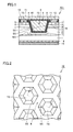
- a silicon carbide semiconductor device in the present embodiment is a vertical type MOSFET 101 having a trench gate.
- MOSFET 101 includes: a substrate 1 having n type conductivity; and a silicon carbide layer 19 epitaxially formed on a main surface MS of substrate 1.
- Silicon carbide layer 19 includes: a breakdown voltage holding layer 2 having n type conductivity; p type body layers 3; n type source contact layers 4; and contact regions 5 having p type conductivity.
- Substrate 1 is made of silicon carbide having a single-crystal structure of one of hexagonal system and cubic system. Further, substrate 1 is provided with main surface MS having an off angle of 5° or smaller relative to a reference plane.
- the reference plane is a ⁇ 000-1 ⁇ plane, more preferably, a (000-1) plane.
- the reference plane is a ⁇ 111 ⁇ plane. Preferably, the off angle thereof is 0.5° or greater.
- Silicon carbide layer 19 has a main surface TS substantially parallel to main surface MS of substrate 1.
- Trench 6 has side surfaces SS.
- Trench 6 has a tapering shape getting wider toward the opening.
- side surfaces SS are inclined relative to main surface TS.
- Each of side surfaces SS has a portion formed by p type body layer 3 and constituting a channel surface of MOSFET 101.
- Side surface SS has a specific crystal plane. Specifically, in the case of the hexagonal system, each of side surfaces SS substantially includes one of a ⁇ 0-33-8 ⁇ plane and a ⁇ 01-1-4 ⁇ plane. In the case of the cubic system, each of side surfaces SS substantially includes a ⁇ 100 ⁇ plane.
- the existence of trench 6 corresponds to existence of a mesa structure having main surface TS as a top surface.
- this top surface has a hexagonal shape as shown in Fig. 2 in the case of the hexagonal system, and has a rectangle or square shape in the case of the cubic system.
- the semiconductor device includes gate insulating films 8, a gate electrode 9, interlayer insulating films 10, source electrodes 12, a source wire electrode 13, a drain electrode 14, and a backside surface protecting electrode 15.
- Breakdown voltage holding layer 2 is formed on one main surface of substrate 1.
- Each of p type body layers 3 is formed on breakdown voltage holding layer 2.
- n type source contact layers 4 are formed on p type body layer 3.
- P type contact region 5 is formed to be surrounded by n type source contact layers 4.
- Gate insulating film 8 is formed on side surfaces SS and a bottom surface of trench 6. Gate insulating film 8 extends onto the upper surface of each of n type source contact layers 4. Gate electrode 9 is formed on gate insulating film 8 to fill the inside of trench 6 (i.e., fill the space between adjacent mesa structures). Gate electrode 9 has an upper surface substantially as high as the upper surface of a portion of gate insulating film 8 on the upper surface of each of n type source contact layers 4.
- Interlayer insulating film 10 is formed to cover gate electrode 9 as well as the portion of gate insulating film 8 on the upper surface of each of n type source contact layers 4. By removing portions of interlayer insulating film 10 and gate insulating film 8, openings 11 are formed to expose portions of n type source contact layers 4 and p type contact regions 5. Source electrodes 12 are formed in contact with p type contact regions 5 and the portions of n type source contact layers 4 so as to fill the inside of openings 11. Source wire electrode 13 is formed in contact with the upper surface of each of source electrodes 12 so as to extend on the upper surface of interlayer insulating film 10. Further, drain electrode 14 is formed on the backside surface of substrate 1 opposite to its main surface on which breakdown voltage holding layer 2 is formed. This drain electrode 14 is an ohmic electrode. Drain electrode 14 has a surface which is opposite to its surface facing substrate 1 and on which backside surface protecting electrode 15 is formed.
- each of side surfaces SS (side walls of the mesa structure) of trench 6 substantially corresponds to a ⁇ 0-33-8 ⁇ plane.
- the crystal plane constituting side surface SS is a plane having an off angle of not less than -3° and not more than 3°, more preferably, not less than -1° and not more than 1° relative to the ⁇ 0-33-8 ⁇ plane in the ⁇ 1-100> direction. Because each of such side surfaces SS corresponds to the stable crystal plane, a higher channel mobility can be obtained when employed for the channel surface, as compared with a case where another crystal plane (for example, a (0001) plane) is employed therefor. In addition, leakage current is reduced and high breakdown voltage is obtained.
- MOSFET 101 The following describes a method for manufacturing MOSFET 101.
- Substrate 1 ( Fig. 3 ) formed of silicon carbide is first prepared.
- main surface MS of substrate 1 substantially corresponds to a ⁇ 000-1 ⁇ plane.
- the main surface MS thereof substantially corresponds to a ⁇ 111 ⁇ plane.
- silicon carbide layer 19 provided with main surface TS is formed on substrate 1.
- silicon carbide layer 19 having n type conductivity is formed on substrate 1.
- This epitaxial growth can be performed using a CVD (Chemical Vapor Deposition) method that utilizes a mixed gas of silane (SiH 4 ) and propane (C 3 H 8 ) as a material gas and utilizes hydrogen gas (H 2 ) as a carrier gas, for example.
- CVD Chemical Vapor Deposition
- SiH 4 silane
- propane C 3 H 8
- H 2 hydrogen gas
- N nitrogen
- P phosphorus
- the concentration of the impurity can be, for example, not less than 5 ⁇ 10 15 cm -3 and not more than 5 ⁇ 10 16 cm -3 .
- breakdown voltage holding layer 2, p type body layer 3, and n type source contact layer 4 are formed from silicon carbide layer 19. Specifically, ions are implanted into the upper surface layer of silicon carbide layer 19, thereby forming p type body layer 3 and n type source contact layer 4. A portion thereof having not been through the ion implantation serves as breakdown voltage holding layer 2. In the ion implantation for forming p type body layer 3, ions of an impurity for providing p type conductivity such as aluminum (Al) are implanted. In doing so, by adjusting acceleration energy of the ions to be implanted, the depth of the region in which p type body layer 3 is to be formed can be adjusted.
- Al aluminum
- ions of an impurity for providing n type conductivity are implanted into breakdown voltage holding layer 2 thus having p type body layer 3 formed therein, thereby forming n type source contact layer 4.
- An exemplary, usable impurity for providing n type conductivity is phosphorus (P) or the like.
- masks 17 are formed to cover portions of main surface TS of silicon carbide layer 19.
- an insulating film such as a silicon oxide film can be used.
- the following process can be employed, for example. That is, a silicon oxide film is formed on the upper surface of n type source contact layer 4 by means of the CVD method or the like. Then, a resist film (not shown) having a predetermined opening pattern is formed on the silicon oxide film by means of the photolithography method. Using the resist film as a mask, a portion of the silicon oxide film is removed by etching. Thereafter, the resist film is removed. As a result, masks 17 having an opening pattern are formed.
- a recess 16 having side surfaces substantially perpendicular to main surface TS of silicon carbide layer 19 is formed.
- RIE reactive ion etching
- ICP inductively coupled plasma
- the ICP-RIE can be employed using, as a reactive gas, a SF 6 or a mixed gas of SF 6 and O 2 .
- thermal etching refers to etching that employs chemical reaction taking place by supplying a process gas containing a reactive gas to a heated object to be etched.
- chlorine-based gas preferably, chlorine gas is used as the reactive gas.
- the thermal etching is preferably performed in an atmosphere in which the chlorine-based gas has a partial pressure of 50% or smaller. Further, the thermal etching is preferably performed in an atmosphere with reduced pressure.
- the atmosphere with reduced pressure has a pressure of not more than 1/10 of the atmospheric pressure.
- the thermal etching is preferably performed under a condition that substrate 1 having silicon carbide layer 19 provided thereon has a temperature (heat treatment temperature) of 1000°C or greater.
- a mixed gas of oxygen gas and chlorine gas is used as a reactive gas.
- the etching is performed at a heat treatment temperature of, for example, not less than 700°C and not more than 1200°C.
- the heat treatment temperature is not less than 700°C and not more than 1200°C.
- a quartz member can be used for a device for the heat treatment.
- the upper limit of the temperature is more preferably 1100°C, further preferably 1000°C.
- the lower limit of the temperature is more preferably 800°C, further preferably 900°C.
- the etching rate can be a sufficiently practical value in the thermal etching step of forming the surface including the ⁇ 0-33-8 ⁇ plane, the ⁇ 01-1-4 ⁇ plane, or the ⁇ 100 ⁇ plane. Accordingly, the treatment time in this step can be sufficiently short.
- main reaction proceeds under conditions that x and y satisfy 0.5 ⁇ x ⁇ 2.0 and 1.0 ⁇ y ⁇ 2.0 in a reaction formula represented as SiC + mO 2 + nCl 2 ⁇ SiCl x + CO y , where m, n, x, and y are positive numbers.
- the reaction (thermal etching) proceeds the most.
- m and n described above respectively represent amounts of the oxygen gas and the chlorine gas actually reacting, and are therefore different from amounts of the oxygen gas and the chlorine gas supplied as the process gas.
- a ratio of a flow rate of oxygen to a flow rate of chlorine in this thermal etching is preferably not less than 0.1 and not more than 2.0. More preferably, the lower limit of this ratio is 0.25. In this case, a surface including the ⁇ 0-33-8 ⁇ plane, the ⁇ 01-1-4 ⁇ plane, or the ⁇ 100 ⁇ plane can be securely formed.
- the reaction gas may contain a carrier gas in addition to the chlorine gas and the oxygen gas.
- An exemplary, usable carrier gas is nitrogen (N 2 ) gas, argon gas, helium gas, or the like.
- the crystal plane exhibited in side surface SS may be substantially the ⁇ 0-33-8 ⁇ plane. Namely, in the etching under the above-described conditions, side surface SS of trench 6 is spontaneously formed to correspond to the ⁇ 0-33-8 ⁇ plane, which is a crystal plane allowing for the slowest etching rate. As a result, a structure shown in Fig. 9 is obtained. It should be noted that the crystal plane constituting side surface SS may be the ⁇ 01-1-4 ⁇ plane. Meanwhile, in the case of the cubic system, the crystal plane constituting side surface SS may be the ⁇ 100 ⁇ plane.
- mask 17 ( Fig. 8 and Fig. 9 ) is removed by means of an appropriate method such as etching.
- contact regions 5 and electric field relaxing region 7 are formed.
- a resist film (not shown) having a predetermined pattern is first formed using the photolithography method so as to extend from the inside of trench 6 onto each of the upper surfaces of n type source contact layers 4.
- the resist film there can be used a resist film having an opening pattern in conformity with the bottom portion of trench 6 and a portion of the upper surface of each of n type source contact layers 4.
- electric field relaxing region 7 is formed at the bottom portion of trench 6 and contact region 5 of p type conductivity is formed at the region of the portion of n type source contact layer 4. Thereafter, the resist film is removed.
- trench 6 has a planar shape in the form of a mesh constituted of unit cells (each defined by annular portion of trench 6 surrounding one mesa structure) each having a hexagonal planar shape.
- p type contact region 5 is disposed substantially at the central portion of the upper surface of each of the mesa structures as shown in Fig. 11 .
- p type contact region 5 has a planar shape similar to the shape of outer circumference of the upper surface of the mesa structure, i.e., has a hexagonal planar shape.
- an activation annealing step is performed to activate the impurity implanted by means of the above-described ion implantation.
- the annealing treatment is performed without forming any particular cap layer on the surface of the epitaxial layer made of silicon carbide (for example, on the side wall of the mesa structure).
- the inventors have found that even when the activation annealing treatment is performed without forming a protecting film such as the cap layer on the surface thereof in the case where the above-described ⁇ 0-33-8 ⁇ plane is employed, a property of the surface is never deteriorated and sufficient surface smoothness can be maintained.
- the conventionally required step of forming the protecting film (cap layer) before the activation annealing treatment is omitted and the activation annealing step is directly performed.
- the above-described cap layer may be formed before performing the activation annealing step.
- the cap layer may be provided only on the upper surfaces of n type source contact layer 4 and p type contact region 5 before performing the activation annealing treatment.
- gate insulating film 8 is formed on side surfaces SS of silicon carbide layer 19. Specifically, gate insulating film 8 is formed to extend from the inside of trench 6 onto the upper surfaces of n type source contact layer 4 and p type contact region 5.
- gate insulating film 8 for example, there can be used an oxide film (silicon oxide film) obtained by thermally oxidizing silicon carbide layer 19.
- gate electrode 9 is formed to face each of side surfaces SS of silicon carbide layer 19 with gate insulating film 8 being interposed therebetween. Specifically, gate electrode 9 is formed on gate insulating film 8 to fill the inside of trench 6.
- a method for forming gate electrode 9 the following method can be used, for example. First, a sputtering method or the like is employed to form a conductor film on gate insulating film 8.
- the conductor film is to be the gate electrode extending to the inside of trench 6 and to a region on p type contact region 5.
- the conductor film can be made of any material such as a metal as long as the material has conductivity.
- an appropriate method such as an etch back method or a CMP (Chemical Mechanical Polishing) method is used to remove a portion of the conductor film formed on regions other than the inside of trench 6.
- an appropriate method such as an etch back method or a CMP (Chemical Mechanical Polishing) method is used to remove a portion of the conductor film formed on regions other than the inside of trench 6.
- CMP Chemical Mechanical Polishing
- interlayer insulating film 10 is formed to cover the upper surface of gate electrode 9 and the upper surface of gate insulating film 8 exposed on p type contact region 5.
- Interlayer insulating film 10 can be made of any material as long as the material is insulative.
- a resist film (not shown) having a pattern is formed on interlayer insulating film 10, using the photolithography method.
- the resist film is provided with an opening pattern formed in conformity with a region on p type contact region 5.
- portions of interlayer insulating film 10 and gate insulating film 8 are removed by means of etching.
- openings 11 are formed to extend through interlayer insulating film 10 and gate insulating film 8.
- Each of openings 11 has a bottom portion at which p type contact region 5 and a portion of n type source contact layer 4 are exposed.
- This source electrode 12 is an ohmic electrode making ohmic contact with p type contact region 5 and n type source contact layer 4.
- drain electrode 14 is formed on the backside surface of substrate 1 (the surface thereof opposite to the main surface thereof on which breakdown voltage holding layer 2 is formed). Drain electrode 14 can be made of any material as long as the material allows for ohmic contact with substrate 1.
- Source wire electrode 13 makes contact with the upper surface of source electrode 12, and extends on the upper surface of interlayer insulating film 10.
- Backside surface protecting electrode 15 is formed on the surface of drain electrode 14. As a result, MOSFET 101 is obtained.
- the thermal etching is performed in the atmosphere in which the chlorine-based gas has a partial pressure of 50% or smaller. Accordingly, an amount of the chlorine-based gas supplied to the surface to be etched is restricted. As a result, progress of etching is suppressed at the portion having high chemical stability, and etching of the portion having low chemical stability mainly proceeds. Accordingly, the plane orientation of side surface SS formed in silicon carbide layer 19 by means of etching can be made closer to the specific crystal plane.
- the thermal etching is performed in the atmosphere with reduced pressure. Accordingly, the amount of the chlorine-based gas supplied to the surface to be etched is restricted. As a result, progress of etching is suppressed at the portion having high chemical stability, and etching mainly proceeds at the portion having low chemical stability. Accordingly, the plane orientation of side surface SS formed in silicon carbide layer 19 by means of etching can be made closer to the specific crystal plane.
- the atmosphere with reduced pressure has a pressure of not more than 1/10 of the atmospheric pressure. Accordingly, the amount of chlorine-based gas supplied to the surface to be etched is sufficiently restricted.
- the thermal etching is performed at 1000°C or greater. Accordingly, the surface to be etched is chemically activated, whereby an amount of consumption of chlorine-based gas in the etching becomes large at this surface. Hence, the amount of chlorine-based gas having an etching ability is restricted on the surface to be etched. As a result, progress of etching is suppressed at the portion having high chemical stability, and etching of the portion having low chemical stability mainly proceeds. Accordingly, the plane orientation of side surface SS formed in silicon carbide layer 19 by means of etching can be made closer to the specific crystal plane.
- gate insulating film 8 is formed on side surface SS of silicon carbide layer 19, and gate electrode 9 is formed to face side surface SS of silicon carbide layer 19 with gate insulating film 8 being interposed therebetween.
- side surface SS having a plane orientation closer to the specific crystal plane can be used as the channel surface controlled by gate electrode 9. Accordingly, variation of channel mobility can be suppressed.
- the specific crystal plane is adapted to attain high channel mobility, high channel mobility can be obtained stably.
- mask 17 is suitably shaped to be hexagonal. This hexagonal arrangement might be deviated from an ideal arrangement 17i to an arrangement 17r as indicated by arrows in the figure. In this case, if the conditions of the thermal etching in the present embodiment are used, a desired side surface SS can be obtained irrespective of some deviation because the specific crystal plane is highly likely to spontaneously formed.
- side surface SS In the case of employing inappropriate thermal etching conditions under which not only the portion having low chemical stability but also the portion having high chemical stability are noticeably etched (in the case of a comparative example), side surfaces SSz less straight are likely to be formed when viewed in a plan view as shown in Fig. 16 . In contrast, according to the present embodiment, the specific crystal plane is spontaneously formed, thus forming side surfaces SS more straight when viewed in a plan view as shown in Fig. 17 . Fig. 18 and Fig. 19 respectively show microphotographs of the silicon carbide layers of the comparative example and the example.
- trench 6 of MOSFET 101 has the flat bottom surface
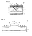
- a V-shaped trench may be provided such as a trench 6V ( Fig. 20 ) of a MOSFET 101v.
- MOSFETs can be integrated more.
- a PiN diode 102 serving as a silicon carbide semiconductor device of the present embodiment includes a substrate 1, and a silicon carbide layer having an n - epitaxial layer 42 and a p + semiconductor layer 43.
- Substrate 1 has n type conductivity.
- N - epitaxial layer 42 has n type conductivity, and has an impurity concentration lower than the concentration of a conductive impurity of substrate 1.
- P + semiconductor layer 43 is provided on n - epitaxial layer 42.
- the silicon carbide layer is provided with a mesa structure 44 having a main surface TS serving as a top surface, and side surfaces SS.
- the silicon carbide layer has a surface constituted of n - epitaxial layer 42 so as to surround this mesa structure 44. On this surface, guard rings 45 are provided. Each of guard rings 45 has p type conductivity.
- Each of side surfaces SS is constituted by a specific crystal plane (for example, a ⁇ 03-3-8 ⁇ plane).
- mesa structure 44 has six planes equivalent to the specific crystal plane ( ⁇ 03-3-8 ⁇ plane).
- PiN diode 102 has a current path extending between main surface TS of the silicon carbide layer and substrate 1 in the thickness direction of the silicon carbide layer (vertical direction in the figure).
- side surfaces SS are located between the main surface TS side and the substrate 1 side corresponding to ends of PiN diode 102.
- leakage current which flows via the surface of the silicon carbide layer, flows on side surfaces SS.
- each of side surfaces SS is adapted to have a plane orientation close to the specific crystal plane as described above, current is stably suppressed and is less likely to flow on side surfaces SS. Accordingly, leakage current of diode 102 can be stably suppressed to a low value. Further, when the specific crystal plane is adapted to attain a low interface state density, leakage current can be suppressed stably.
- Substrate 1 is prepared.
- substrate 1 for example, there can be used a substrate made of silicon carbide of hexagonal crystal type.
- N - epitaxial layer 42 is formed on the main surface of substrate 1 using an epitaxy method.
- ions of an impurity for providing p type conductivity are implanted, thereby forming a p type semiconductor layer, which is to be p + semiconductor layer 43.
- a mask pattern made of a silicon oxide film and in the form of an island is formed on a region to serve as mesa structure 44.
- This mask pattern may be adapted to have, for example, a hexagonal planar shape, but may have any other shape (such as a round shape or a quadrangular shape).
- portions of p + semiconductor layer 43 and n - epitaxial layer 42 are removed by means of etching.
- a projection portion to serve as mesa structure 44 is formed below the mask pattern (corresponding to Fig. 7 of the first embodiment).
- thermal etching similar to that in the first embodiment is performed to etch the side surfaces of the projection portion, thereby forming side surfaces SS. Thereafter, the mask pattern is removed. Next, guard rings 45 are formed by means of ion implantation. Next, activation annealing treatment is performed. In the activation annealing treatment, the heating treatment may be performed without forming a cap layer that at least covers side surfaces SS.
- a PiN diode 102v may be used which is provided with JTE (Junction Termination Extension) regions 46.
- JTE regions 46 has p type conductivity, and is disposed on n - epitaxial layer 42 so as to be connected to p + semiconductor layer 43.
- side surface SS includes one of the ⁇ 03-3-8 ⁇ plane, the ⁇ 01-1-4 ⁇ plane, and the ⁇ 100 ⁇ plane
- side surface SS includes one of the ⁇ 03-3-8 ⁇ plane, the ⁇ 01-1-4 ⁇ plane, and the ⁇ 100 ⁇ plane
- the plurality of crystal planes include one of the ⁇ 03-3-8 ⁇ plane, the ⁇ 01-1-4 ⁇ plane, and the ⁇ 100 ⁇ plane. This will be specifically described and illustrated with reference to the case where side surface SS includes the ⁇ 03-3-8 ⁇ plane and another plane.
- Each of side surfaces SS may correspond to a chemically stable plane constituted by, for example, alternately providing a plane 56a and a plane 56b in the side surface of trench 6 as shown in Fig. 23 , microscopically.
- Plane 56a has a plane orientation of ⁇ 0-33-8 ⁇
- plane 56b which is connected to plane 56a, has a plane orientation different from that of plane 56a.
- the term “microscopically” refers to "minutely to such an extent that at least the size about twice as large as an interatomic spacing is considered”.
- plane 56b has a plane orientation of ⁇ 0-11-1 ⁇ .
- plane 56b in Fig. 23 may have a length (width) twice as large as, for example, the interatomic spacing of Si atoms (or C atoms).
- the silicon carbide semiconductor device is not limited to these, and may be, for example, an IGBT (Insulated Gate Bipolar Transistor). It should be also noted that a configuration may be employed in which n type conductivity and p type conductivity in each of the above-described configurations are replaced with each other.
- IGBT Insulated Gate Bipolar Transistor
Landscapes
- Electrodes Of Semiconductors (AREA)
- Drying Of Semiconductors (AREA)
- Physics & Mathematics (AREA)
- Engineering & Computer Science (AREA)
- Plasma & Fusion (AREA)
Abstract
Description
- The present invention relates to a method for manufacturing a silicon carbide semiconductor device, more particularly, a method for manufacturing a silicon carbide semiconductor device including a silicon carbide layer having an inclined side surface.
- Conventionally, it has been proposed to use silicon carbide (SiC) as a material for a semiconductor device. For example, it is proposed to use silicon carbide to form a trench gate type MOSFET (Metal Oxide Semiconductor Field Effect Transistor) (see Japanese Patent Laying-Open No.
2008-235546 - In this publication, it is proposed to form tapering side walls of a gate trench in order to improve breakdown voltage of a gate insulating film. Specifically, a semiconductor layer made of silicon carbide is partially removed by anisotropic etching using an etching mask having an opening pattern, and then is subjected to isotropic etching, whereby the gate trench formed in the semiconductor layer is provided with the tapering side walls.
- PTL 1: Japanese Patent Laying-Open No.
2008-235546 - When the side walls (side surfaces) of the gate trench are formed by means of isotropic etching as disclosed in this publication, it is difficult for each of the side surfaces to have a plane orientation sufficiently close to a specific crystal plane. If the side surface can be adapted to have a plane orientation close to such a specific crystal plane, various advantages can be obtained. For example, when a crystal plane allowing for high electron mobility is selected, a MOSFET having a low on-resistance can be obtained by increasing channel mobility.
- The present invention has been made to solve the foregoing problem, and has its object to provide a method for manufacturing a silicon carbide semiconductor device including a silicon carbide layer having a side surface whose plane orientation can be made closer to a specific crystal plane.
- A method for manufacturing a silicon carbide semiconductor device in one aspect of the present invention includes the following steps. A silicon carbide layer provided with a main surface is formed on a substrate. A mask is formed to cover a portion of the main surface of the silicon carbide layer. The main surface of the silicon carbide layer on which the mask is formed is thermally etched using chlorine-based gas so as to provide the silicon carbide layer with a side surface inclined relative to the main surface. The step of thermally etching is performed in an atmosphere in which the chlorine-based gas has a partial pressure of 50% or smaller.
- According to the manufacturing method according to the above-described one aspect, the thermal etching is performed in the atmosphere in which the chlorine-based gas has a partial pressure of 50% or smaller. Accordingly, an amount of chlorine-based gas supplied to the surface to be etched is restricted. As a result, progress of etching is suppressed at a portion having high chemical stability, and etching of a portion having low chemical stability mainly proceeds. Accordingly, the plane orientation of the side surface formed in the silicon carbide layer by means of etching can be made closer to the specific crystal plane.
- In the manufacturing method according to the above-described one aspect, the step of thermally etching is preferably performed in an atmosphere with reduced pressure. Accordingly, the amount of chlorine-based gas supplied to the surface to be etched is restricted. As a result, progress of etching is suppressed at the portion having high chemical stability, and etching of the portion having low chemical stability mainly proceeds. Accordingly, the plane orientation of the side surface formed in the silicon carbide layer by means of etching can be made closer to the specific crystal plane.
- In the manufacturing method according to the above-described one aspect, the step of thermally etching is preferably performed at 1000°C or greater. Accordingly, the surface to be etched is chemically activated, whereby an amount of consumption of chlorine-based gas in the etching becomes large at this surface. Hence, the amount of chlorine-based gas having an etching ability is restricted on the surface to be etched. As a result, progress of etching is suppressed at the portion having high chemical stability, and etching of the portion having low chemical stability mainly proceeds. Accordingly, the plane orientation of the side surface formed in the silicon carbide layer by means of etching can be made closer to the specific crystal plane.
- A method for manufacturing a silicon carbide semiconductor device in another aspect of the present invention includes the following steps. A silicon carbide layer provided with a main surface is formed on a substrate. A mask is formed to cover a portion of the main surface of the silicon carbide layer. The main surface of the silicon carbide layer on which the mask is formed is thermally etched using chlorine-based gas so as to provide the silicon carbide layer with a side surface inclined relative to the main surface. The step of thermally etching is performed in an atmosphere with reduced pressure.
- According to the manufacturing method according to the above-described another aspect, the thermal etching is performed in the atmosphere with reduced pressure. Accordingly, an amount of chlorine-based gas supplied to the surface to be etched is restricted. As a result, progress of etching is suppressed at a portion having high chemical stability, and etching of a portion having low chemical stability mainly proceeds. Accordingly, the plane orientation of the side surface formed in the silicon carbide layer by means of etching can be made closer to the specific crystal plane.
- In the manufacturing method according to the above-described another aspect, the atmosphere with reduced pressure preferably has a pressure of not more than 1/10 of an atmospheric pressure. Accordingly, the amount of chlorine-based gas supplied to the surface to be etched is sufficiently restricted.
- In the manufacturing method according to the above-described another aspect, the step of thermally etching is preferably performed in an atmosphere in which the chlorine-based gas has a partial pressure of 50% or smaller. Accordingly, the amount of chlorine-based gas supplied to the surface to be etched is restricted. As a result, progress of etching is suppressed at the portion having high chemical stability, and etching of the portion having low chemical stability mainly proceeds. Accordingly, the plane orientation of the side surface formed in the silicon carbide layer by means of etching can be made closer to the specific crystal plane.
- In the manufacturing method according to the above-described another aspect, the step of thermally etching is preferably performed at 1000°C or greater. Accordingly, the surface to be etched is chemically activated, whereby an amount of consumption of chlorine-based gas in the etching becomes large at this surface. Hence, the amount of chlorine-based gas having an etching ability is restricted on the surface to be etched. As a result, progress of etching is suppressed at the portion having high chemical stability, and etching of the portion having low chemical stability mainly proceeds. Accordingly, the plane orientation of the side surface formed in the silicon carbide layer by means of etching can be made closer to the specific crystal plane.
- A method for manufacturing a silicon carbide semiconductor device in still another aspect of the present invention includes the following steps. A silicon carbide layer provided with a main surface is formed on a substrate. A mask is formed to cover a portion of the main surface of the silicon carbide layer. The main surface of the silicon carbide layer on which the mask is formed is thermally etched using chlorine-based gas so as to provide the silicon carbide layer with a side surface inclined relative to the main surface. The step of thermally etching is performed at 1000°C or greater.
- According to the manufacturing method according to the above-described still another aspect, the thermal etching is performed at 1000°C or greater. Accordingly, the surface to be etched is chemically activated, whereby an amount of consumption of chlorine-based gas in the etching becomes large at this surface. Hence, the amount of chlorine-based gas having an etching ability is restricted on the surface to be etched. As a result, progress of etching is suppressed at a portion having high chemical stability, and etching of a portion having low chemical stability mainly proceeds. Accordingly, the plane orientation of the side surface formed in the silicon carbide layer by means of etching can be made closer to the specific crystal plane.
- In the manufacturing method according to the above-described still another aspect, the step of thermally etching is preferably performed in an atmosphere in which the chlorine-based gas has a partial pressure of 50% or smaller. Accordingly, the amount of chlorine-based gas supplied to the surface to be etched is further restricted. As a result, progress of etching is suppressed at the portion having high chemical stability, and etching of the portion having low chemical stability mainly proceeds. Accordingly, the plane orientation of the side surface formed in the silicon carbide layer by means of etching can be made closer to the specific crystal plane.
- In the manufacturing method according to the above-described still another aspect, the step of thermally etching is preferably performed in an atmosphere with reduced pressure. Accordingly, the amount of chlorine-based gas supplied to the surface to be etched is restricted. As a result, progress of etching is suppressed at the portion having high chemical stability, and etching of the portion having low chemical stability mainly proceeds. Accordingly, the plane orientation of the side surface formed in the silicon carbide layer by means of etching can be made closer to the specific crystal plane.
- Preferably, the method for manufacturing the silicon carbide semiconductor device further includes the following steps. A gate insulating film is formed on the side surface of the silicon carbide layer. Then, a gate electrode is formed to face the side surface of the silicon carbide layer with the gate insulating film being interposed therebetween. In this way, the side surface having a plane orientation closer to the specific crystal plane can be used as a channel surface controlled by the gate electrode. Accordingly, variation of channel mobility can be suppressed. When the specific crystal plane is adapted to attain high channel mobility, high channel mobility can be obtained stably.
- Preferably, the silicon carbide semiconductor device is a diode having a current path extending between the main surface of the silicon carbide layer and the substrate in a thickness direction of the silicon carbide layer. In this case, the side surface is located between the main surface side and the substrate side corresponding to ends of the diode. Hence, leakage current, which flows via the surface of the silicon carbide layer, flows on the side surface. When the side surface is adapted to have a plane orientation close to the specific crystal plane as described above, current is stably suppressed and is less likely to flow on the side surface. Accordingly, the leakage current of the diode can be stably suppressed to a low value. Further, when the specific crystal plane is adapted to attain a low interface state density, leakage current can be suppressed stably.
- As described above, according to the present invention, the plane orientation of the side surface of the silicon carbide layer included in the silicon carbide semiconductor device can be made closer to the specific crystal plane.
-
-
Fig. 1 is a partial cross sectional view schematically showing a configuration of a silicon carbide semiconductor device in a first embodiment of the present invention. -
Fig. 2 is a partial plan view schematically showing a configuration of a silicon carbide layer provided in the silicon carbide semiconductor device ofFig. 1 . -
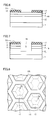
Fig. 3 is a partial cross sectional view schematically showing a first step of a method for manufacturing the silicon carbide semiconductor device ofFig. 1 . -
Fig. 4 is a partial cross sectional view schematically showing a second step of the method for manufacturing the silicon carbide semiconductor device ofFig. 1 . -
Fig. 5 is a partial plan view schematically showing a third step of the method for manufacturing the silicon carbide semiconductor device ofFig. 1 . -
Fig. 6 is a partial cross sectional view schematically showing the third step of the method for manufacturing the silicon carbide semiconductor device ofFig. 1 . -
Fig. 7 is a partial cross sectional view schematically showing a fourth step of the method for manufacturing the silicon carbide semiconductor device ofFig. 1 . -
Fig. 8 is a partial plan view schematically showing a fifth step of the method for manufacturing the silicon carbide semiconductor device ofFig. 1 . -
Fig. 9 is a partial cross sectional view schematically showing the fifth step of the method for manufacturing the silicon carbide semiconductor device ofFig. 1 . -
Fig. 10 is a partial cross sectional view schematically showing a sixth step of the method for manufacturing the silicon carbide semiconductor device ofFig. 1 . -
Fig. 11 is a partial perspective view schematically showing the sixth step of the method for manufacturing the silicon carbide semiconductor device ofFig. 1 . -
Fig. 12 is a partial cross sectional view schematically showing a seventh step of the method for manufacturing the silicon carbide semiconductor device ofFig. 1 . -
Fig. 13 is a partial cross sectional view schematically showing an eight step of the method for manufacturing the silicon carbide semiconductor device ofFig. 1 . -
Fig. 14 is a partial cross sectional view schematically showing a ninth step of the method for manufacturing the silicon carbide semiconductor device ofFig. 1 . -
Fig. 15 is a plan view for illustrating deviation of rotation of a mask. -
Fig. 16 is a partial plan view schematically showing the shape of a side surface of a silicon carbide layer in a comparative example. -
Fig. 17 is a partial plan view schematically showing the shape of the side surface of the silicon carbide layer in the present embodiment. -
Fig. 18 is a microphotograph of the silicon carbide layer in the comparative example. -
Fig. 19 is a microphotograph of the silicon carbide layer in the example. -
Fig. 20 is a partial cross sectional view schematically showing a variation ofFig. 1 . -
Fig. 21 is a partial cross sectional view schematically showing a configuration of a silicon carbide semiconductor device in a second embodiment of the present invention. -
Fig. 22 is a partial cross sectional view schematically showing a variation ofFig. 21 . -
Fig. 23 is a partial cross sectional view schematically showing one example of the side surface of the silicon carbide layer. - The following describes embodiments of the present invention with reference to figures. It should be noted that in the below-mentioned figures, the same or corresponding portions are given the same reference characters and are not described repeatedly. Further, regarding crystallographic indications in the present specification, an individual orientation is represented by [], a group orientation is represented by ◇, and an individual plane is represented by (), and a group plane is represented by {}. In addition, a negative index is supposed to be crystallographically indicated by putting "-" (bar) above a numeral, but is indicated by putting the negative sign before the numeral in the present specification. For description of an angle, a system in which an omnidirectional angle is 360° is employed.
- As shown in
Fig. 1 and Fig. 2 , a silicon carbide semiconductor device in the present embodiment is avertical type MOSFET 101 having a trench gate.MOSFET 101 includes: asubstrate 1 having n type conductivity; and asilicon carbide layer 19 epitaxially formed on a main surface MS ofsubstrate 1.Silicon carbide layer 19 includes: a breakdownvoltage holding layer 2 having n type conductivity; p type body layers 3; n type source contact layers 4; andcontact regions 5 having p type conductivity. -
Substrate 1 is made of silicon carbide having a single-crystal structure of one of hexagonal system and cubic system. Further,substrate 1 is provided with main surface MS having an off angle of 5° or smaller relative to a reference plane. In the case of the hexagonal system, the reference plane is a {000-1} plane, more preferably, a (000-1) plane. In the case of the cubic system, the reference plane is a {111} plane. Preferably, the off angle thereof is 0.5° or greater. -
Silicon carbide layer 19 has a main surface TS substantially parallel to main surface MS ofsubstrate 1.Trench 6 has side surfaces SS.Trench 6 has a tapering shape getting wider toward the opening. Hence, side surfaces SS are inclined relative to main surface TS. Each of side surfaces SS has a portion formed by ptype body layer 3 and constituting a channel surface ofMOSFET 101. Side surface SS has a specific crystal plane. Specifically, in the case of the hexagonal system, each of side surfaces SS substantially includes one of a {0-33-8} plane and a {01-1-4} plane. In the case of the cubic system, each of side surfaces SS substantially includes a {100} plane. - From a different point of view, the existence of
trench 6 corresponds to existence of a mesa structure having main surface TS as a top surface. Preferably, this top surface has a hexagonal shape as shown inFig. 2 in the case of the hexagonal system, and has a rectangle or square shape in the case of the cubic system. - Further, the semiconductor device includes
gate insulating films 8, agate electrode 9,interlayer insulating films 10,source electrodes 12, asource wire electrode 13, adrain electrode 14, and a backsidesurface protecting electrode 15. - The following describes details of the semiconductor device. Breakdown
voltage holding layer 2 is formed on one main surface ofsubstrate 1. Each of p type body layers 3 is formed on breakdownvoltage holding layer 2. On ptype body layer 3, n type source contact layers 4 are formed. Ptype contact region 5 is formed to be surrounded by n type source contact layers 4. By removing portions of n type source contact layers 4, ptype body layer 3, and breakdownvoltage holding layer 2, mesa structures surrounded bytrench 6 are formed. -
Gate insulating film 8 is formed on side surfaces SS and a bottom surface oftrench 6.Gate insulating film 8 extends onto the upper surface of each of n type source contact layers 4.Gate electrode 9 is formed ongate insulating film 8 to fill the inside of trench 6 (i.e., fill the space between adjacent mesa structures).Gate electrode 9 has an upper surface substantially as high as the upper surface of a portion ofgate insulating film 8 on the upper surface of each of n type source contact layers 4. -
Interlayer insulating film 10 is formed to covergate electrode 9 as well as the portion ofgate insulating film 8 on the upper surface of each of n type source contact layers 4. By removing portions of interlayer insulatingfilm 10 andgate insulating film 8,openings 11 are formed to expose portions of n type source contact layers 4 and ptype contact regions 5.Source electrodes 12 are formed in contact with ptype contact regions 5 and the portions of n type source contact layers 4 so as to fill the inside ofopenings 11.Source wire electrode 13 is formed in contact with the upper surface of each ofsource electrodes 12 so as to extend on the upper surface ofinterlayer insulating film 10. Further,drain electrode 14 is formed on the backside surface ofsubstrate 1 opposite to its main surface on which breakdownvoltage holding layer 2 is formed. Thisdrain electrode 14 is an ohmic electrode.Drain electrode 14 has a surface which is opposite to itssurface facing substrate 1 and on which backsidesurface protecting electrode 15 is formed. - When
silicon carbide layer 19 has a hexagonal crystal structure, each of side surfaces SS (side walls of the mesa structure) oftrench 6 substantially corresponds to a {0-33-8} plane. Specifically, the crystal plane constituting side surface SS is a plane having an off angle of not less than -3° and not more than 3°, more preferably, not less than -1° and not more than 1° relative to the {0-33-8} plane in the <1-100> direction. Because each of such side surfaces SS corresponds to the stable crystal plane, a higher channel mobility can be obtained when employed for the channel surface, as compared with a case where another crystal plane (for example, a (0001) plane) is employed therefor. In addition, leakage current is reduced and high breakdown voltage is obtained. - The following describes a method for manufacturing
MOSFET 101. - Substrate 1 (
Fig. 3 ) formed of silicon carbide is first prepared. In the case of the hexagonal system, main surface MS ofsubstrate 1 substantially corresponds to a {000-1} plane. In the case of the cubic system, the main surface MS thereof substantially corresponds to a {111} plane. - As shown in
Fig. 3 , onsubstrate 1,silicon carbide layer 19 provided with main surface TS is formed. Specifically, by means of epitaxial growth on main surface MS ofsubstrate 1,silicon carbide layer 19 having n type conductivity is formed. This epitaxial growth can be performed using a CVD (Chemical Vapor Deposition) method that utilizes a mixed gas of silane (SiH4) and propane (C3H8) as a material gas and utilizes hydrogen gas (H2) as a carrier gas, for example. In doing so, it is preferable to introduce nitrogen (N) or phosphorus (P) as an impurity for providingsilicon carbide layer 19 with n type conductivity, for example. The concentration of the impurity can be, for example, not less than 5 × 1015 cm-3 and not more than 5 × 1016 cm-3. - As shown in
Fig. 4 , breakdownvoltage holding layer 2, ptype body layer 3, and n typesource contact layer 4 are formed fromsilicon carbide layer 19. Specifically, ions are implanted into the upper surface layer ofsilicon carbide layer 19, thereby forming ptype body layer 3 and n typesource contact layer 4. A portion thereof having not been through the ion implantation serves as breakdownvoltage holding layer 2. In the ion implantation for forming ptype body layer 3, ions of an impurity for providing p type conductivity such as aluminum (Al) are implanted. In doing so, by adjusting acceleration energy of the ions to be implanted, the depth of the region in which ptype body layer 3 is to be formed can be adjusted. Further, ions of an impurity for providing n type conductivity are implanted into breakdownvoltage holding layer 2 thus having ptype body layer 3 formed therein, thereby forming n typesource contact layer 4. An exemplary, usable impurity for providing n type conductivity is phosphorus (P) or the like. - As shown in
Fig. 5 andFig. 6 , masks 17 are formed to cover portions of main surface TS ofsilicon carbide layer 19. As each ofmasks 17, for example, an insulating film such as a silicon oxide film can be used. As a method for formingmask 17, the following process can be employed, for example. That is, a silicon oxide film is formed on the upper surface of n typesource contact layer 4 by means of the CVD method or the like. Then, a resist film (not shown) having a predetermined opening pattern is formed on the silicon oxide film by means of the photolithography method. Using the resist film as a mask, a portion of the silicon oxide film is removed by etching. Thereafter, the resist film is removed. As a result, masks 17 having an opening pattern are formed. - As shown in
Fig. 7 , arecess 16 having side surfaces substantially perpendicular to main surface TS ofsilicon carbide layer 19 is formed. Specifically, usingmasks 17, portions of n typesource contact layer 4, ptype body layer 3, and breakdownvoltage holding layer 2 are etched. Exemplary, usable etching is reactive ion etching (RIE) or ion milling. As the RIE, inductively coupled plasma (ICP) RIE can be used in particular. Specifically, for example, the ICP-RIE can be employed using, as a reactive gas, a SF6 or a mixed gas of SF6 and O2. - As shown in
Fig. 8 andFig. 9 ,trench 6 is formed to providesilicon carbide layer 19 with side surfaces SS inclined relative to main surface TS. Specifically, main surface TS ofsilicon carbide layer 19 on which masks 17 are formed is subjected to thermal etching. Here, the term "thermal etching" refers to etching that employs chemical reaction taking place by supplying a process gas containing a reactive gas to a heated object to be etched. In the present embodiment, chlorine-based gas, preferably, chlorine gas is used as the reactive gas. Further, the thermal etching is preferably performed in an atmosphere in which the chlorine-based gas has a partial pressure of 50% or smaller. Further, the thermal etching is preferably performed in an atmosphere with reduced pressure. More preferably, the atmosphere with reduced pressure has a pressure of not more than 1/10 of the atmospheric pressure. Further, the thermal etching is preferably performed under a condition thatsubstrate 1 havingsilicon carbide layer 19 provided thereon has a temperature (heat treatment temperature) of 1000°C or greater. - The following describes an example of the thermal etching in detail.
- Regarding the process gas, a mixed gas of oxygen gas and chlorine gas is used as a reactive gas. The etching is performed at a heat treatment temperature of, for example, not less than 700°C and not more than 1200°C. Preferably, the heat treatment temperature is not less than 700°C and not more than 1200°C. In the case where the heat treatment temperature is 1200°C or smaller, a quartz member can be used for a device for the heat treatment. The upper limit of the temperature is more preferably 1100°C, further preferably 1000°C. The lower limit of the temperature is more preferably 800°C, further preferably 900°C. In this case, the etching rate can be a sufficiently practical value in the thermal etching step of forming the surface including the {0-33-8} plane, the {01-1-4} plane, or the {100} plane. Accordingly, the treatment time in this step can be sufficiently short.
- Here, in the thermal etching step, main reaction proceeds under conditions that x and y satisfy 0.5 ≤ x ≤ 2.0 and 1.0 ≤ y ≤ 2.0 in a reaction formula represented as SiC + mO2 + nCl2 → SiClx + COy, where m, n, x, and y are positive numbers. Under conditions that x = 4 and y = 2, the reaction (thermal etching) proceeds the most. It should be noted that m and n described above respectively represent amounts of the oxygen gas and the chlorine gas actually reacting, and are therefore different from amounts of the oxygen gas and the chlorine gas supplied as the process gas. The present inventors have found that a ratio of a flow rate of oxygen to a flow rate of chlorine in this thermal etching is preferably not less than 0.1 and not more than 2.0. More preferably, the lower limit of this ratio is 0.25. In this case, a surface including the {0-33-8} plane, the {01-1-4} plane, or the {100} plane can be securely formed.
- It should be noted that the reaction gas may contain a carrier gas in addition to the chlorine gas and the oxygen gas. An exemplary, usable carrier gas is nitrogen (N2) gas, argon gas, helium gas, or the like. When the heat treatment temperature is set at not less than 700°C and not more than 1000°C as described above, a rate of etching SiC is approximately, for example, 70 µm/hr. Further, when using silicon oxide (SiO2) as
mask 17 in this case, a selection ratio of SiC to SiO2 can be very large. Accordingly,mask 17 made of SiO2 is not substantially etched during etching of SiC. - It should be noted that in the case of the hexagonal system, the crystal plane exhibited in side surface SS may be substantially the {0-33-8} plane. Namely, in the etching under the above-described conditions, side surface SS of
trench 6 is spontaneously formed to correspond to the {0-33-8} plane, which is a crystal plane allowing for the slowest etching rate. As a result, a structure shown inFig. 9 is obtained. It should be noted that the crystal plane constituting side surface SS may be the {01-1-4} plane. Meanwhile, in the case of the cubic system, the crystal plane constituting side surface SS may be the {100} plane. - Next, mask 17 (
Fig. 8 andFig. 9 ) is removed by means of an appropriate method such as etching. - As shown in
Fig. 10 and Fig. 11 ,contact regions 5 and electricfield relaxing region 7 are formed. Specifically, a resist film (not shown) having a predetermined pattern is first formed using the photolithography method so as to extend from the inside oftrench 6 onto each of the upper surfaces of n type source contact layers 4. As the resist film, there can be used a resist film having an opening pattern in conformity with the bottom portion oftrench 6 and a portion of the upper surface of each of n type source contact layers 4. By implanting ions of an impurity for providing p type conductivity using this resist film as a mask, electricfield relaxing region 7 is formed at the bottom portion oftrench 6 and contactregion 5 of p type conductivity is formed at the region of the portion of n typesource contact layer 4. Thereafter, the resist film is removed. - As seen from
Fig. 11 ,trench 6 has a planar shape in the form of a mesh constituted of unit cells (each defined by annular portion oftrench 6 surrounding one mesa structure) each having a hexagonal planar shape. Further, ptype contact region 5 is disposed substantially at the central portion of the upper surface of each of the mesa structures as shown inFig. 11 . Further, ptype contact region 5 has a planar shape similar to the shape of outer circumference of the upper surface of the mesa structure, i.e., has a hexagonal planar shape. - Next, an activation annealing step is performed to activate the impurity implanted by means of the above-described ion implantation. In this activation annealing step, the annealing treatment is performed without forming any particular cap layer on the surface of the epitaxial layer made of silicon carbide (for example, on the side wall of the mesa structure). Here, the inventors have found that even when the activation annealing treatment is performed without forming a protecting film such as the cap layer on the surface thereof in the case where the above-described {0-33-8} plane is employed, a property of the surface is never deteriorated and sufficient surface smoothness can be maintained. Thus, the conventionally required step of forming the protecting film (cap layer) before the activation annealing treatment is omitted and the activation annealing step is directly performed. It should be noted that the above-described cap layer may be formed before performing the activation annealing step. Alternatively, for example, the cap layer may be provided only on the upper surfaces of n type
source contact layer 4 and ptype contact region 5 before performing the activation annealing treatment. - As shown in
Fig. 12 ,gate insulating film 8 is formed on side surfaces SS ofsilicon carbide layer 19. Specifically,gate insulating film 8 is formed to extend from the inside oftrench 6 onto the upper surfaces of n typesource contact layer 4 and ptype contact region 5. Asgate insulating film 8, for example, there can be used an oxide film (silicon oxide film) obtained by thermally oxidizingsilicon carbide layer 19. - As shown in
Fig. 13 ,gate electrode 9 is formed to face each of side surfaces SS ofsilicon carbide layer 19 withgate insulating film 8 being interposed therebetween. Specifically,gate electrode 9 is formed ongate insulating film 8 to fill the inside oftrench 6. As a method for forminggate electrode 9, the following method can be used, for example. First, a sputtering method or the like is employed to form a conductor film ongate insulating film 8. The conductor film is to be the gate electrode extending to the inside oftrench 6 and to a region on ptype contact region 5. The conductor film can be made of any material such as a metal as long as the material has conductivity. Thereafter, an appropriate method such as an etch back method or a CMP (Chemical Mechanical Polishing) method is used to remove a portion of the conductor film formed on regions other than the inside oftrench 6. As a result, the conductor film filling the inside oftrench 6 remains to constitutegate electrode 9. - Referring to
Fig. 14 ,interlayer insulating film 10 is formed to cover the upper surface ofgate electrode 9 and the upper surface ofgate insulating film 8 exposed on ptype contact region 5.Interlayer insulating film 10 can be made of any material as long as the material is insulative. Further, a resist film (not shown) having a pattern is formed oninterlayer insulating film 10, using the photolithography method. The resist film is provided with an opening pattern formed in conformity with a region on ptype contact region 5. Using this resist film as a mask, portions of interlayer insulatingfilm 10 andgate insulating film 8 are removed by means of etching. As a result, openings 11 (seeFig. 14 ) are formed to extend throughinterlayer insulating film 10 andgate insulating film 8. Each ofopenings 11 has a bottom portion at which ptype contact region 5 and a portion of n typesource contact layer 4 are exposed. - Thereafter, a conductor film is formed to fill the inside of opening 11 and cover the upper surface of the above-described resist film. Thereafter, the resist film is removed using a chemical solution or the like, thereby simultaneously removing (lifting off) the portion of the conductor film formed on the resist film. As a result, the conductor film filling the inside of opening 11 constitutes
source electrode 12. This source electrode 12 is an ohmic electrode making ohmic contact with ptype contact region 5 and n typesource contact layer 4. - Further,
drain electrode 14 is formed on the backside surface of substrate 1 (the surface thereof opposite to the main surface thereof on which breakdownvoltage holding layer 2 is formed).Drain electrode 14 can be made of any material as long as the material allows for ohmic contact withsubstrate 1. - Referring to
Fig. 1 again, an appropriate method such as the sputtering method is employed to formsource wire electrode 13 and backsidesurface protecting electrode 15.Source wire electrode 13 makes contact with the upper surface ofsource electrode 12, and extends on the upper surface ofinterlayer insulating film 10. Backsidesurface protecting electrode 15 is formed on the surface ofdrain electrode 14. As a result,MOSFET 101 is obtained. - According to the present embodiment, the thermal etching is performed in the atmosphere in which the chlorine-based gas has a partial pressure of 50% or smaller. Accordingly, an amount of the chlorine-based gas supplied to the surface to be etched is restricted. As a result, progress of etching is suppressed at the portion having high chemical stability, and etching of the portion having low chemical stability mainly proceeds. Accordingly, the plane orientation of side surface SS formed in
silicon carbide layer 19 by means of etching can be made closer to the specific crystal plane. - Further, the thermal etching is performed in the atmosphere with reduced pressure. Accordingly, the amount of the chlorine-based gas supplied to the surface to be etched is restricted. As a result, progress of etching is suppressed at the portion having high chemical stability, and etching mainly proceeds at the portion having low chemical stability. Accordingly, the plane orientation of side surface SS formed in
silicon carbide layer 19 by means of etching can be made closer to the specific crystal plane. Preferably, the atmosphere with reduced pressure has a pressure of not more than 1/10 of the atmospheric pressure. Accordingly, the amount of chlorine-based gas supplied to the surface to be etched is sufficiently restricted. - Further, the thermal etching is performed at 1000°C or greater. Accordingly, the surface to be etched is chemically activated, whereby an amount of consumption of chlorine-based gas in the etching becomes large at this surface. Hence, the amount of chlorine-based gas having an etching ability is restricted on the surface to be etched. As a result, progress of etching is suppressed at the portion having high chemical stability, and etching of the portion having low chemical stability mainly proceeds. Accordingly, the plane orientation of side surface SS formed in
silicon carbide layer 19 by means of etching can be made closer to the specific crystal plane. - Further,
gate insulating film 8 is formed on side surface SS ofsilicon carbide layer 19, andgate electrode 9 is formed to face side surface SS ofsilicon carbide layer 19 withgate insulating film 8 being interposed therebetween. In this way, side surface SS having a plane orientation closer to the specific crystal plane can be used as the channel surface controlled bygate electrode 9. Accordingly, variation of channel mobility can be suppressed. When the specific crystal plane is adapted to attain high channel mobility, high channel mobility can be obtained stably. - The following describes occurrence of deviation of rotation of mask 17 (
Fig. 5 ) with reference toFig. 15 . When silicon carbide layer 19 (Fig. 6 ) is of hexagonal system,mask 17 is suitably shaped to be hexagonal. This hexagonal arrangement might be deviated from anideal arrangement 17i to anarrangement 17r as indicated by arrows in the figure. In this case, if the conditions of the thermal etching in the present embodiment are used, a desired side surface SS can be obtained irrespective of some deviation because the specific crystal plane is highly likely to spontaneously formed. - The following describes the shape of side surface SS. In the case of employing inappropriate thermal etching conditions under which not only the portion having low chemical stability but also the portion having high chemical stability are noticeably etched (in the case of a comparative example), side surfaces SSz less straight are likely to be formed when viewed in a plan view as shown in
Fig. 16 . In contrast, according to the present embodiment, the specific crystal plane is spontaneously formed, thus forming side surfaces SS more straight when viewed in a plan view as shown inFig. 17 .Fig. 18 and Fig. 19 respectively show microphotographs of the silicon carbide layers of the comparative example and the example. - It should be noted that although
trench 6 ofMOSFET 101 has the flat bottom surface, a V-shaped trench may be provided such as atrench 6V (Fig. 20 ) of aMOSFET 101v. In this case, MOSFETs can be integrated more. - As shown in
Fig. 21 , aPiN diode 102 serving as a silicon carbide semiconductor device of the present embodiment includes asubstrate 1, and a silicon carbide layer having an n- epitaxial layer 42 and a p+ semiconductor layer 43.Substrate 1 has n type conductivity. N- epitaxial layer 42 has n type conductivity, and has an impurity concentration lower than the concentration of a conductive impurity ofsubstrate 1. P+ semiconductor layer 43 is provided on n- epitaxial layer 42. The silicon carbide layer is provided with amesa structure 44 having a main surface TS serving as a top surface, and side surfaces SS. The silicon carbide layer has a surface constituted of n- epitaxial layer 42 so as to surround thismesa structure 44. On this surface, guard rings 45 are provided. Each of guard rings 45 has p type conductivity. - Each of side surfaces SS is constituted by a specific crystal plane (for example, a {03-3-8} plane). Namely,
mesa structure 44 has six planes equivalent to the specific crystal plane ({03-3-8} plane). -
PiN diode 102 has a current path extending between main surface TS of the silicon carbide layer andsubstrate 1 in the thickness direction of the silicon carbide layer (vertical direction in the figure). In this case, side surfaces SS are located between the main surface TS side and thesubstrate 1 side corresponding to ends ofPiN diode 102. Hence, leakage current, which flows via the surface of the silicon carbide layer, flows on side surfaces SS. When each of side surfaces SS is adapted to have a plane orientation close to the specific crystal plane as described above, current is stably suppressed and is less likely to flow on side surfaces SS. Accordingly, leakage current ofdiode 102 can be stably suppressed to a low value. Further, when the specific crystal plane is adapted to attain a low interface state density, leakage current can be suppressed stably. - The following describes a method for manufacturing
PiN diode 102.Substrate 1 is prepared. Assubstrate 1, for example, there can be used a substrate made of silicon carbide of hexagonal crystal type. N- epitaxial layer 42 is formed on the main surface ofsubstrate 1 using an epitaxy method. Into the front side of n- epitaxial layer 42, ions of an impurity for providing p type conductivity are implanted, thereby forming a p type semiconductor layer, which is to be p+ semiconductor layer 43. - Thereafter, on a region to serve as
mesa structure 44, a mask pattern made of a silicon oxide film and in the form of an island is formed. This mask pattern may be adapted to have, for example, a hexagonal planar shape, but may have any other shape (such as a round shape or a quadrangular shape). With this mask pattern formed, portions of p+ semiconductor layer 43 and n- epitaxial layer 42 are removed by means of etching. As a result, a projection portion to serve asmesa structure 44 is formed below the mask pattern (corresponding toFig. 7 of the first embodiment). - Next, thermal etching similar to that in the first embodiment is performed to etch the side surfaces of the projection portion, thereby forming side surfaces SS. Thereafter, the mask pattern is removed. Next, guard rings 45 are formed by means of ion implantation. Next, activation annealing treatment is performed. In the activation annealing treatment, the heating treatment may be performed without forming a cap layer that at least covers side surfaces SS.
- In this way,
PiN diode 102 is obtained. - It should be noted that as shown in
Fig. 22 , aPiN diode 102v may be used which is provided with JTE (Junction Termination Extension)regions 46. Each ofJTE regions 46 has p type conductivity, and is disposed on n- epitaxial layer 42 so as to be connected to p+ semiconductor layer 43. - It should be noted that in the present specification, the case where side surface SS includes one of the {03-3-8} plane, the {01-1-4} plane, and the {100} plane is intended to encompass a case where there are a plurality of crystal planes constituting side surface SS and the plurality of crystal planes include one of the {03-3-8} plane, the {01-1-4} plane, and the {100} plane. This will be specifically described and illustrated with reference to the case where side surface SS includes the {03-3-8} plane and another plane.
- Each of side surfaces SS may correspond to a chemically stable plane constituted by, for example, alternately providing a
plane 56a and aplane 56b in the side surface oftrench 6 as shown inFig. 23 , microscopically.Plane 56a has a plane orientation of {0-33-8} whereasplane 56b, which is connected toplane 56a, has a plane orientation different from that ofplane 56a. Here, the term "microscopically" refers to "minutely to such an extent that at least the size about twice as large as an interatomic spacing is considered". Preferably,plane 56b has a plane orientation of {0-11-1}. Further,plane 56b inFig. 23 may have a length (width) twice as large as, for example, the interatomic spacing of Si atoms (or C atoms). - It should be noted that the MOSFET and the PiN diode have been described in detail above, but the silicon carbide semiconductor device is not limited to these, and may be, for example, an IGBT (Insulated Gate Bipolar Transistor). It should be also noted that a configuration may be employed in which n type conductivity and p type conductivity in each of the above-described configurations are replaced with each other.
- The embodiments disclosed herein are illustrative and non-restrictive in any respect. The scope of claims of the present invention is defined by the terms of the claims, rather than the embodiments described above, and is intended to include any modifications within the scope and meaning equivalent to the terms of the claims.
- 1: substrate; 2: breakdown voltage holding layer; 3: p type body layer; 4: n type source contact layer; 5: contact region; 6, 6V: trench; 7: electric field relaxing region; 8: gate insulating film; 9: gate electrode; 10: interlayer insulating film; 11: opening; 12: source electrode; 13: source wire electrode; 14: drain electrode; 15: backside surface protecting electrode; 17: mask; 19: silicon carbide layer; 42: n- epitaxial layer; 43: p+ semiconductor layer; 44: mesa structure; 101: MOSFET (silicon carbide semiconductor device); 102: PiN diode.
Claims (12)
- A method for manufacturing a silicon carbide semiconductor device (101), comprising the steps of:forming a silicon carbide layer (19) on a substrate (1), said silicon carbide layer (19) being provided with a main surface (TS);forming a mask (17) covering a portion of said main surface of said silicon carbide layer; andthermally etching said main surface of said silicon carbide layer on which said mask is formed, using chlorine-based gas so as to provide said silicon carbide layer with a side surface (SS) inclined relative to said main surface, the step of thermally etching being performed in an atmosphere in which said chlorine-based gas has a partial pressure of 50% or smaller.
- The method for manufacturing the silicon carbide semiconductor device according to claim 1, wherein the step of thermally etching is performed in an atmosphere with reduced pressure.
- The method for manufacturing the silicon carbide semiconductor device according to claim 1 or 2, wherein the step of thermally etching is performed at 1000°C or greater.
- A method for manufacturing a silicon carbide semiconductor device (101), comprising:forming a silicon carbide layer (19) on a substrate (1), said silicon carbide layer (19) being provided with a main surface (TS);forming a mask (17) covering a portion of said main surface of said silicon carbide layer; andthermally etching said main surface of said silicon carbide layer on which said mask is formed, using chlorine-based gas so as to provide said silicon carbide layer with a side surface (SS) inclined relative to said main surface, the step of thermally etching being performed in an atmosphere with reduced pressure.
- The method for manufacturing the silicon carbide semiconductor device according to claim 4, wherein said atmosphere with reduced pressure has a pressure of not more than 1/10 of an atmospheric pressure.
- The method for manufacturing the silicon carbide semiconductor device according to claim 4 or 5, wherein the step of thermally etching is performed in an atmosphere in which said chlorine-based gas has a partial pressure of 50% or smaller.
- The method for manufacturing the silicon carbide semiconductor device according to any one of claims 4-6, wherein the step of thermally etching is performed at 1000°C or greater.
- A method for manufacturing a silicon carbide semiconductor device (101), comprising the steps of:forming a silicon carbide layer (19) on a substrate (1), said silicon carbide layer (19) being provided with a main surface (TS);forming a mask (17) covering a portion of said main surface of said silicon carbide layer; andthermally etching said main surface of said silicon carbide layer on which said mask is formed, using chlorine-based gas so as to provide said silicon carbide layer with a side surface (SS) inclined relative to said main surface, the step of thermally etching being performed at 1000°C or greater.
- The method for manufacturing the silicon carbide semiconductor device according to claim 8, wherein the step of thermally etching is performed in an atmosphere in which said chlorine-based gas has a partial pressure of 50% or smaller.
- The method for manufacturing the silicon carbide semiconductor device according to claim 8 or 9, wherein the step of thermally etching is performed in an atmosphere with reduced pressure.
- The method for manufacturing the silicon carbide semiconductor device according to any one of claims 1-10, further comprising the steps of:forming a gate insulating film (8) on said side surface of said silicon carbide layer; andforming a gate electrode (9) facing said side surface of said silicon carbide layer with said gate insulating film being interposed therebetween.
- The method for manufacturing the silicon carbide semiconductor device according to any one of claims 1-10, wherein said silicon carbide semiconductor device is a diode having a current path extending between said main surface of said silicon carbide layer and said substrate in a thickness direction of said silicon carbide layer.
Applications Claiming Priority (2)
| Application Number | Priority Date | Filing Date | Title |
|---|---|---|---|
| JP2011253614A JP5764046B2 (en) | 2011-11-21 | 2011-11-21 | Method for manufacturing silicon carbide semiconductor device |
| PCT/JP2012/075516 WO2013077089A1 (en) | 2011-11-21 | 2012-10-02 | Method for manufacturing silicon carbide semiconductor device |
Publications (2)
| Publication Number | Publication Date |
|---|---|
| EP2784805A1 true EP2784805A1 (en) | 2014-10-01 |
| EP2784805A4 EP2784805A4 (en) | 2015-08-05 |
Family
ID=48427348
Family Applications (1)
| Application Number | Title | Priority Date | Filing Date |
|---|---|---|---|
| EP12851007.0A Withdrawn EP2784805A4 (en) | 2011-11-21 | 2012-10-02 | METHOD FOR MANUFACTURING SEMICONDUCTOR DEVICE OF SILICON CARBIDE |
Country Status (5)
| Country | Link |
|---|---|
| US (1) | US8999854B2 (en) |
| EP (1) | EP2784805A4 (en) |
| JP (1) | JP5764046B2 (en) |
| CN (1) | CN103890921A (en) |
| WO (1) | WO2013077089A1 (en) |
Families Citing this family (12)
| Publication number | Priority date | Publication date | Assignee | Title |
|---|---|---|---|---|
| US9252261B2 (en) * | 2011-04-19 | 2016-02-02 | Nissan Motor Co., Ltd. | Semiconductor device and manufacturing method of the same |
| EP2750198A4 (en) | 2011-08-26 | 2015-04-15 | Nat Univ Corp Nara Inst | SiC SEMICONDUCTOR ELEMENT AND METHOD FOR MANUFACTURING THE SAME |
| JP5954140B2 (en) * | 2012-11-29 | 2016-07-20 | 住友電気工業株式会社 | Silicon carbide semiconductor device |
| JP2015053428A (en) * | 2013-09-09 | 2015-03-19 | 住友電気工業株式会社 | Method for manufacturing silicon carbide semiconductor device |
| JP2015060859A (en) * | 2013-09-17 | 2015-03-30 | 住友電気工業株式会社 | Silicon carbide semiconductor device and method for manufacturing silicon carbide semiconductor device |
| JP2015076592A (en) * | 2013-10-11 | 2015-04-20 | 住友電気工業株式会社 | Silicon carbide semiconductor device and manufacturing method of the same |
| CN108140676B (en) * | 2015-10-30 | 2020-12-18 | 三菱电机株式会社 | Silicon carbide semiconductor devices |
| JP7166053B2 (en) * | 2017-12-21 | 2022-11-07 | 株式会社東芝 | Semiconductor devices, inverter circuits, drive devices, vehicles, and elevators |
| JP7230477B2 (en) * | 2018-12-12 | 2023-03-01 | 株式会社デンソー | Manufacturing method of trench gate type switching element |
| US12159905B2 (en) * | 2019-11-11 | 2024-12-03 | Sumitomo Electric Industries, Ltd. | Silicon carbide semiconductor device |
| EP4152011B1 (en) * | 2020-05-14 | 2025-03-12 | NTT Advanced Technology Corporation | Standard sample and method for producing same |
| US11677023B2 (en) * | 2021-05-04 | 2023-06-13 | Infineon Technologies Austria Ag | Semiconductor device |
Family Cites Families (60)
| Publication number | Priority date | Publication date | Assignee | Title |
|---|---|---|---|---|
| JP3471473B2 (en) | 1994-04-06 | 2003-12-02 | 株式会社デンソー | Semiconductor device and manufacturing method thereof |
| JP3531291B2 (en) | 1994-06-23 | 2004-05-24 | 株式会社デンソー | Method for manufacturing silicon carbide semiconductor device |
| JP3419163B2 (en) | 1995-09-06 | 2003-06-23 | 株式会社デンソー | Method for manufacturing silicon carbide semiconductor device |
| FR2738394B1 (en) | 1995-09-06 | 1998-06-26 | Nippon Denso Co | SILICON CARBIDE SEMICONDUCTOR DEVICE, AND MANUFACTURING METHOD THEREOF |
| US6133587A (en) | 1996-01-23 | 2000-10-17 | Denso Corporation | Silicon carbide semiconductor device and process for manufacturing same |
| JP3471509B2 (en) | 1996-01-23 | 2003-12-02 | 株式会社デンソー | Silicon carbide semiconductor device |
| US5882786A (en) | 1996-11-15 | 1999-03-16 | C3, Inc. | Gemstones formed of silicon carbide with diamond coating |
| JPH11251592A (en) | 1998-01-05 | 1999-09-17 | Denso Corp | Silicon carbide semiconductor device |
| JP2000021849A (en) * | 1998-07-06 | 2000-01-21 | Shin Etsu Handotai Co Ltd | Dry etching method |
| JP4457432B2 (en) | 1999-06-17 | 2010-04-28 | 株式会社デンソー | Seed crystal and silicon carbide single crystal production method, silicon carbide single crystal and single crystal production apparatus using the same |
| US6734461B1 (en) | 1999-09-07 | 2004-05-11 | Sixon Inc. | SiC wafer, SiC semiconductor device, and production method of SiC wafer |
| EP1684359A3 (en) | 2000-05-31 | 2006-10-25 | Matsushita Electrical Industrial Co., Ltd | Misfet |
| US20020177321A1 (en) | 2001-03-30 | 2002-11-28 | Li Si Yi | Plasma etching of silicon carbide |
| JP2005056868A (en) | 2001-06-04 | 2005-03-03 | Matsushita Electric Ind Co Ltd | Method for manufacturing silicon carbide semiconductor device |
| US20030012925A1 (en) | 2001-07-16 | 2003-01-16 | Motorola, Inc. | Process for fabricating semiconductor structures and devices utilizing the formation of a compliant substrate for materials used to form the same and including an etch stop layer used for back side processing |
| JP2003133434A (en) | 2001-10-23 | 2003-05-09 | Mitsubishi Electric Corp | Semiconductor integrated circuit |
| JP2003218350A (en) | 2002-01-22 | 2003-07-31 | Hitachi Ltd | Semiconductor device and manufacturing method thereof |
| JP4593099B2 (en) | 2003-03-10 | 2010-12-08 | 学校法人関西学院 | Liquid crystal epitaxial growth method of single crystal silicon carbide and heat treatment apparatus used therefor |
| US20060249073A1 (en) | 2003-03-10 | 2006-11-09 | The New Industry Research Organization | Method of heat treatment and heat treatment apparatus |
| JP2005167035A (en) | 2003-12-03 | 2005-06-23 | Kansai Electric Power Co Inc:The | Silicon carbide semiconductor device and manufacturing method thereof |
| JP4500558B2 (en) | 2004-02-09 | 2010-07-14 | トヨタ自動車株式会社 | Insulated gate type semiconductor device manufacturing method |
| JP4487655B2 (en) * | 2004-04-14 | 2010-06-23 | 株式会社デンソー | Manufacturing method of semiconductor device |
| JPWO2005116307A1 (en) | 2004-05-27 | 2008-04-03 | 株式会社ブリヂストン | Method for manufacturing silicon carbide single crystal wafer |
| JP5017768B2 (en) | 2004-05-31 | 2012-09-05 | 富士電機株式会社 | Silicon carbide semiconductor element |
| ATE459979T1 (en) * | 2004-06-30 | 2010-03-15 | Xycarb Ceramics Bv | METHOD FOR SURFACE TREATMENT OF A METAL CARBIDE SUBSTRATE FOR USE IN SEMICONDUCTOR MANUFACTURING PROCESSES AND A METAL CARBIDE SUBSTRATE ITSELF |
| JP2007182330A (en) | 2004-08-24 | 2007-07-19 | Bridgestone Corp | Silicon carbide single crystal wafer and manufacturing method thereof |
| JP4872217B2 (en) | 2005-02-16 | 2012-02-08 | 富士電機株式会社 | Method for manufacturing silicon carbide semiconductor element |
| JP2006303469A (en) | 2005-03-25 | 2006-11-02 | Shindengen Electric Mfg Co Ltd | SiC semiconductor device |
| US20060214268A1 (en) | 2005-03-25 | 2006-09-28 | Shindengen Electric Manufacturing Co., Ltd. | SiC semiconductor device |
| JP4986420B2 (en) | 2005-07-05 | 2012-07-25 | 三菱電機株式会社 | Transistor |
| JP2007035823A (en) | 2005-07-26 | 2007-02-08 | Elpida Memory Inc | Trench formation method, semiconductor device manufacturing method, and semiconductor device |
| JP2007053227A (en) | 2005-08-18 | 2007-03-01 | Matsushita Electric Ind Co Ltd | Semiconductor device and manufacturing method thereof |
| JP5017823B2 (en) | 2005-09-12 | 2012-09-05 | 富士電機株式会社 | Manufacturing method of semiconductor device |
| JP5017855B2 (en) | 2005-12-14 | 2012-09-05 | 富士電機株式会社 | Manufacturing method of semiconductor device |
| US8664664B2 (en) | 2006-01-10 | 2014-03-04 | Cree, Inc. | Silicon carbide dimpled substrate |
| JP2007243080A (en) | 2006-03-13 | 2007-09-20 | Fuji Electric Holdings Co Ltd | Semiconductor device and manufacturing method thereof |
| JP5034315B2 (en) | 2006-05-19 | 2012-09-26 | 三菱電機株式会社 | Semiconductor device and manufacturing method thereof |
| JP2008098593A (en) | 2006-09-15 | 2008-04-24 | Ricoh Co Ltd | Semiconductor device and manufacturing method thereof |
| WO2008062729A1 (en) | 2006-11-21 | 2008-05-29 | Sumitomo Electric Industries, Ltd. | Silicon carbide semiconductor device and process for producing the same |
| JP2008135534A (en) | 2006-11-28 | 2008-06-12 | Toyota Motor Corp | Method for manufacturing a semiconductor substrate having a bottomed groove |
| JP4046140B1 (en) | 2006-11-29 | 2008-02-13 | 住友電気工業株式会社 | Method for manufacturing silicon carbide semiconductor device |
| JP4450241B2 (en) | 2007-03-20 | 2010-04-14 | 株式会社デンソー | Method for manufacturing silicon carbide semiconductor device |
| JP2009170456A (en) | 2008-01-10 | 2009-07-30 | Sumitomo Electric Ind Ltd | Manufacturing method of semiconductor device |
| JP2010147222A (en) | 2008-12-18 | 2010-07-01 | Denso Corp | Silicon carbide semiconductor device and method of manufacturing the same |
| EP2091083A3 (en) | 2008-02-13 | 2009-10-14 | Denso Corporation | Silicon carbide semiconductor device including a deep layer |
| JP5589263B2 (en) | 2008-05-29 | 2014-09-17 | 富士電機株式会社 | Method for forming trench in silicon carbide semiconductor substrate |
| JP5298691B2 (en) | 2008-07-31 | 2013-09-25 | 住友電気工業株式会社 | Silicon carbide semiconductor device and manufacturing method thereof |
| JP5442229B2 (en) | 2008-09-04 | 2014-03-12 | ローム株式会社 | Method of manufacturing nitride semiconductor device |
| JP4544360B2 (en) | 2008-10-24 | 2010-09-15 | トヨタ自動車株式会社 | Manufacturing method of IGBT |
| WO2010110253A1 (en) | 2009-03-27 | 2010-09-30 | 住友電気工業株式会社 | Mosfet and method for manufacturing mosfet |
| CN101556919B (en) * | 2009-05-21 | 2014-03-05 | 中国电子科技集团公司第十三研究所 | Method of Controlling Step Morphology of SiC Substrate Etching |
| JP2011044513A (en) | 2009-08-20 | 2011-03-03 | National Institute Of Advanced Industrial Science & Technology | Silicon carbide semiconductor device |
| JP5075280B2 (en) | 2009-10-23 | 2012-11-21 | パナソニック株式会社 | Semiconductor device and manufacturing method thereof |
| JPWO2011115294A1 (en) | 2010-03-16 | 2013-07-04 | 合同会社先端配線材料研究所 | Silicon carbide electrode, silicon carbide semiconductor element, silicon carbide semiconductor device, and method for forming silicon carbide electrode |
| JP5707770B2 (en) | 2010-08-03 | 2015-04-30 | 住友電気工業株式会社 | Semiconductor device and manufacturing method thereof |
| CN102971853B (en) | 2010-08-03 | 2016-06-29 | 住友电气工业株式会社 | Semiconductor device and manufacture method thereof |
| JP5510309B2 (en) | 2010-12-22 | 2014-06-04 | 株式会社デンソー | Silicon carbide semiconductor device and manufacturing method thereof |
| JP5668576B2 (en) * | 2011-04-01 | 2015-02-12 | 住友電気工業株式会社 | Silicon carbide semiconductor device |
| EP2750198A4 (en) | 2011-08-26 | 2015-04-15 | Nat Univ Corp Nara Inst | SiC SEMICONDUCTOR ELEMENT AND METHOD FOR MANUFACTURING THE SAME |
| JP5699878B2 (en) * | 2011-09-14 | 2015-04-15 | 住友電気工業株式会社 | Silicon carbide semiconductor device and manufacturing method thereof |
-
2011
- 2011-11-21 JP JP2011253614A patent/JP5764046B2/en active Active
-
2012
- 2012-10-02 CN CN201280051730.3A patent/CN103890921A/en active Pending
- 2012-10-02 WO PCT/JP2012/075516 patent/WO2013077089A1/en not_active Ceased
- 2012-10-02 EP EP12851007.0A patent/EP2784805A4/en not_active Withdrawn
- 2012-10-23 US US13/658,583 patent/US8999854B2/en active Active
Also Published As
| Publication number | Publication date |
|---|---|
| US8999854B2 (en) | 2015-04-07 |
| JP5764046B2 (en) | 2015-08-12 |
| WO2013077089A1 (en) | 2013-05-30 |
| CN103890921A (en) | 2014-06-25 |
| EP2784805A4 (en) | 2015-08-05 |
| JP2013110243A (en) | 2013-06-06 |
| US20130130482A1 (en) | 2013-05-23 |
Similar Documents
| Publication | Publication Date | Title |
|---|---|---|
| EP2602824B1 (en) | Process for production of semiconductor device | |
| US8999854B2 (en) | Method for manufacturing silicon carbide semiconductor device | |
| US9012922B2 (en) | Silicon carbide semiconductor device and method for manufacturing same | |
| EP2602822B1 (en) | Semiconductor device and process for production thereof | |
| EP2770537B1 (en) | Silicon carbide semiconductor device and method for manufacturing same | |
| EP2763180B1 (en) | Silicon carbide semiconductor device | |
| EP2879186A1 (en) | Silicon carbide semiconductor device | |
| EP2725619A1 (en) | Semiconductor device and method of manufacturing same | |
| US20130065384A1 (en) | Method for manufacturing silicon carbide semiconductor device | |
| EP2784821A1 (en) | Silicon carbide semiconductor device and method for manufacturing same | |
| US20160126347A1 (en) | Silicon carbide semiconductor device | |
| US9299790B2 (en) | Silicon carbide semiconductor device |
Legal Events
| Date | Code | Title | Description |
|---|---|---|---|
| PUAI | Public reference made under article 153(3) epc to a published international application that has entered the european phase |
Free format text: ORIGINAL CODE: 0009012 |
|
| 17P | Request for examination filed |
Effective date: 20140319 |
|
| AK | Designated contracting states |
Kind code of ref document: A1 Designated state(s): AL AT BE BG CH CY CZ DE DK EE ES FI FR GB GR HR HU IE IS IT LI LT LU LV MC MK MT NL NO PL PT RO RS SE SI SK SM TR |
|
| DAX | Request for extension of the european patent (deleted) | ||
| RIC1 | Information provided on ipc code assigned before grant |
Ipc: H01L 29/861 20060101ALI20150317BHEP Ipc: H01L 29/78 20060101ALI20150317BHEP Ipc: H01L 21/04 20060101ALI20150317BHEP Ipc: H01L 21/3065 20060101ALI20150317BHEP Ipc: H01L 21/302 20060101ALI20150317BHEP Ipc: H01L 29/06 20060101ALI20150317BHEP Ipc: H01L 29/423 20060101ALI20150317BHEP Ipc: H01L 29/739 20060101ALI20150317BHEP Ipc: H01L 21/336 20060101AFI20150317BHEP Ipc: H01L 21/329 20060101ALI20150317BHEP Ipc: H01L 29/868 20060101ALI20150317BHEP Ipc: H01L 21/308 20060101ALI20150317BHEP Ipc: H01L 29/12 20060101ALI20150317BHEP Ipc: H01L 29/16 20060101ALI20150317BHEP Ipc: H01L 21/205 20060101ALI20150317BHEP Ipc: H01L 21/02 20060101ALI20150317BHEP Ipc: H01L 29/04 20060101ALI20150317BHEP Ipc: H01L 29/66 20060101ALI20150317BHEP |
|
| RA4 | Supplementary search report drawn up and despatched (corrected) |
Effective date: 20150707 |
|
| RIC1 | Information provided on ipc code assigned before grant |
Ipc: H01L 29/78 20060101ALI20150701BHEP Ipc: H01L 21/02 20060101ALI20150701BHEP Ipc: H01L 29/861 20060101ALI20150701BHEP Ipc: H01L 29/04 20060101ALI20150701BHEP Ipc: H01L 21/302 20060101ALI20150701BHEP Ipc: H01L 21/04 20060101ALI20150701BHEP Ipc: H01L 21/329 20060101ALI20150701BHEP Ipc: H01L 29/16 20060101ALI20150701BHEP Ipc: H01L 21/336 20060101AFI20150701BHEP Ipc: H01L 29/739 20060101ALI20150701BHEP Ipc: H01L 21/205 20060101ALI20150701BHEP Ipc: H01L 29/423 20060101ALI20150701BHEP Ipc: H01L 29/66 20060101ALI20150701BHEP Ipc: H01L 29/06 20060101ALI20150701BHEP Ipc: H01L 21/3065 20060101ALI20150701BHEP Ipc: H01L 29/868 20060101ALI20150701BHEP Ipc: H01L 21/308 20060101ALI20150701BHEP Ipc: H01L 29/12 20060101ALI20150701BHEP |
|
| STAA | Information on the status of an ep patent application or granted ep patent |
Free format text: STATUS: THE APPLICATION IS DEEMED TO BE WITHDRAWN |
|
| 18D | Application deemed to be withdrawn |
Effective date: 20160204 |