EP2782146B1 - Method for manufacturing a solar cell with reduced potential induced degradation - Google Patents
Method for manufacturing a solar cell with reduced potential induced degradation Download PDFInfo
- Publication number
- EP2782146B1 EP2782146B1 EP13174068.0A EP13174068A EP2782146B1 EP 2782146 B1 EP2782146 B1 EP 2782146B1 EP 13174068 A EP13174068 A EP 13174068A EP 2782146 B1 EP2782146 B1 EP 2782146B1
- Authority
- EP
- European Patent Office
- Prior art keywords
- solar cell
- silicon oxide
- oxide film
- film
- manufacturing
- Prior art date
- Legal status (The legal status is an assumption and is not a legal conclusion. Google has not performed a legal analysis and makes no representation as to the accuracy of the status listed.)
- Active
Links
Images


Classifications
-
- H—ELECTRICITY
- H10—SEMICONDUCTOR DEVICES; ELECTRIC SOLID-STATE DEVICES NOT OTHERWISE PROVIDED FOR
- H10F—INORGANIC SEMICONDUCTOR DEVICES SENSITIVE TO INFRARED RADIATION, LIGHT, ELECTROMAGNETIC RADIATION OF SHORTER WAVELENGTH OR CORPUSCULAR RADIATION
- H10F71/00—Manufacture or treatment of devices covered by this subclass
-
- H—ELECTRICITY
- H10—SEMICONDUCTOR DEVICES; ELECTRIC SOLID-STATE DEVICES NOT OTHERWISE PROVIDED FOR
- H10F—INORGANIC SEMICONDUCTOR DEVICES SENSITIVE TO INFRARED RADIATION, LIGHT, ELECTROMAGNETIC RADIATION OF SHORTER WAVELENGTH OR CORPUSCULAR RADIATION
- H10F10/00—Individual photovoltaic cells, e.g. solar cells
- H10F10/10—Individual photovoltaic cells, e.g. solar cells having potential barriers
- H10F10/14—Photovoltaic cells having only PN homojunction potential barriers
-
- H—ELECTRICITY
- H10—SEMICONDUCTOR DEVICES; ELECTRIC SOLID-STATE DEVICES NOT OTHERWISE PROVIDED FOR
- H10F—INORGANIC SEMICONDUCTOR DEVICES SENSITIVE TO INFRARED RADIATION, LIGHT, ELECTROMAGNETIC RADIATION OF SHORTER WAVELENGTH OR CORPUSCULAR RADIATION
- H10F71/00—Manufacture or treatment of devices covered by this subclass
- H10F71/129—Passivating
-
- H—ELECTRICITY
- H10—SEMICONDUCTOR DEVICES; ELECTRIC SOLID-STATE DEVICES NOT OTHERWISE PROVIDED FOR
- H10F—INORGANIC SEMICONDUCTOR DEVICES SENSITIVE TO INFRARED RADIATION, LIGHT, ELECTROMAGNETIC RADIATION OF SHORTER WAVELENGTH OR CORPUSCULAR RADIATION
- H10F77/00—Constructional details of devices covered by this subclass
- H10F77/30—Coatings
- H10F77/306—Coatings for devices having potential barriers
- H10F77/311—Coatings for devices having potential barriers for photovoltaic cells
- H10F77/315—Coatings for devices having potential barriers for photovoltaic cells the coatings being antireflective or having enhancing optical properties
-
- Y—GENERAL TAGGING OF NEW TECHNOLOGICAL DEVELOPMENTS; GENERAL TAGGING OF CROSS-SECTIONAL TECHNOLOGIES SPANNING OVER SEVERAL SECTIONS OF THE IPC; TECHNICAL SUBJECTS COVERED BY FORMER USPC CROSS-REFERENCE ART COLLECTIONS [XRACs] AND DIGESTS
- Y02—TECHNOLOGIES OR APPLICATIONS FOR MITIGATION OR ADAPTATION AGAINST CLIMATE CHANGE
- Y02E—REDUCTION OF GREENHOUSE GAS [GHG] EMISSIONS, RELATED TO ENERGY GENERATION, TRANSMISSION OR DISTRIBUTION
- Y02E10/00—Energy generation through renewable energy sources
- Y02E10/50—Photovoltaic [PV] energy
- Y02E10/547—Monocrystalline silicon PV cells
-
- Y—GENERAL TAGGING OF NEW TECHNOLOGICAL DEVELOPMENTS; GENERAL TAGGING OF CROSS-SECTIONAL TECHNOLOGIES SPANNING OVER SEVERAL SECTIONS OF THE IPC; TECHNICAL SUBJECTS COVERED BY FORMER USPC CROSS-REFERENCE ART COLLECTIONS [XRACs] AND DIGESTS
- Y02—TECHNOLOGIES OR APPLICATIONS FOR MITIGATION OR ADAPTATION AGAINST CLIMATE CHANGE
- Y02P—CLIMATE CHANGE MITIGATION TECHNOLOGIES IN THE PRODUCTION OR PROCESSING OF GOODS
- Y02P70/00—Climate change mitigation technologies in the production process for final industrial or consumer products
- Y02P70/50—Manufacturing or production processes characterised by the final manufactured product
Definitions
- the present invention relates to the technical field of solar cell manufacturing, and in particular to a solar cell of anti potential induced degradation and a manufacturing method thereof
- the photovoltaic module is an apparatus for converting light energy into electrical energy by utilizing photovoltaic effect of the PN junction of silicon material.
- the photovoltaic module includes: a glass backboard and a glass substrate which are arranged oppositely; a solar cell arranged between the glass backboard and the glass substrate; a packaging frame for fixing the glass backboard, the solar cell and the glass substrate; and so on.
- the conventional processes for manufacturing the solar cell include processes such as texturing, diffusion, etching, chemical vapor deposition (i.e., PECVD), screen printing and sintering.
- texturing the surface of the silicon wafer is eroded by using acid or alkali to form different surface patterns, i.e., surface texturization, therefore the light reflectance is reduced, the short-circuit current is increased and the photoelectric conversion efficiency of the solar cell is ultimately improved.
- the impurity diffusion is performed on the silicon wafer to form a PN junction, which acts as a "heart" of the semiconductor device when the semiconductor device operates.
- the etching process the P-type region and N-type region of the silicon wafer are separated from each other.
- the gas containing the atom which composes the film is ionized by using microwave or radio frequency, to form plasma which has strong chemical activity and is prone to chemical reaction, so that a desired anti-reflection film is deposited on the surface of the silicon wafer.
- the screen printing process by using the adhesive tape on the printing blade, slurry is moved through a screen template with an image or a pattern, to print on the surface of the silicon wafer and form a printed electrode.
- the organic component in the slurry is burnt out, so that a good ohmic contact is formed between the slurry and the silicon wafer.
- PID potential induced degradation
- the photovoltaic module operates under a high negative voltage for a long time, so there will be a leakage current passage between the glass substrate and the package material. Therefore, a large number of charges are accumulated on the surface of the solar cell, and the charges accumulated on the surface of the solar cell may draw photogenic charge carriers, leading to leakage current. Therefore, electrical performance parameters of the photovoltaic module, such as the fill factor FF, the short circuit current Jsc and the open circuit voltage Voc are deteriorated, and thus the electrical performance of the photovoltaic module will be lower than the design criteria.
- US 2010/029038 A1 describes a solar cell manufacturing method comprising the step of forming a passivation film on a surface layer of a silicon layer by performing an oxidation process, a nitridation process or an oxynitriding process on the surface layer of the silicon layer by using plasma.
- Document XP040513304 describes a SiOx/SiNx/SiOx stack system for passivating the rear sides of silicon solar cells.
- a solar cell of anti potential induced degradation and a manufacturing method thereof are provided according to embodiments of the invention.
- the solar cell manufactured by using the manufacturing method has a good electrical insulation property with outside packaging material and the glass substrate, so the corresponding photovoltaic module has an anti potential induced degradation effect, which improves the electrical performance of the photovoltaic module operating under the high negative voltage for a long time.
- a method for manufacturing a solar cell of reduced potential induced degradation includes: performing plasma cleaning on a silicon wafer by using an oxidizing gas, so as to form a first silicon oxide film on the surface of the silicon wafer; and forming an anti-reflection film on the surface of the first silicon oxide film, where the anti-reflection film includes at least a silicon oxide film; wherein the forming an anti-reflection film on the surface of the first silicon oxide film comprises: depositing a uniform silicon nitride film on the surface of the first silicon oxide film, and depositing a uniform silicon oxide film on the surface of the silicon nitride film, so as to form the anti-reflection film.
- the oxidizing gas includes at least N 2 O.
- the plasma cleaning lasts for 30s to 900s, inclusive.
- the silicon oxide film in the anti-reflection film is deposited by using a method of PECVD, APCVD or LPCVD.
- the silicon oxide film in the anti-reflection film is formed by gas including N 2 O and SiH 4 , and gas flow ratio of N 2 O to SiH 4 ranges from 1 to 50:1, inclusive.
- the silicon oxide film in the anti-reflection film has a thickness that ranges from 1nm to 150nm, inclusive.
- the silicon nitride film in the anti-reflection film is deposited by using a method of PECVD, APCVD or LPCVD.
- the silicon nitride film in the anti-reflection film is formed by gas including NH 3 and SiH 4 , and gas flow ratio of NH 3 to SiH 4 ranges from 1 to 30:1, inclusive.
- the silicon nitride film in the anti-reflection film has a thickness that ranges from 10nm to 150nm, inclusive.
- the plasma cleaning is firstly performed on the silicon wafer by using the oxidizing gas, so as to form a compact first silicon oxide film on the surface of the silicon wafer while cleaning the silicon wafer; then the anti-reflection film is formed on the surface of the cleaned silicon wafer, i.e., the anti-reflection film is formed on the surface of the first silicon oxide film, where the anti-reflection film includes at least a silicon oxide film.
- the solar cell manufactured by using the manufacturing method provided by the embodiments of the invention has a good electrical insulation property with the packaging material and the glass substrate, so the corresponding photovoltaic module has an anti potential induced degradation effect, which improves the electrical performance of the photovoltaic module operating under the high negative voltage for a long time.
- the potential induced degradation effect is prone to occur, so the electrical performance parameters of the photovoltaic module, such as FF, Jsc and Voc are deteriorated and will be lower than the design criteria when the photovoltaic module operates under the high negative voltage for a long time.
- the inventor has found that there are mainly two reasons which cause the potential induced degradation effect, one is related to the photovoltaic module system and the other is related to the photovoltaic module.
- the photovoltaic module system it is indicated by the research and the actual operation of the power plant that, in a case that all of the photovoltaic modules between the solar cell module in the middle of the solar cell module array and the negative output terminal of the inverter operate under negative bias, the closer the solar cell module is to the negative output terminal of the inverter, the stronger the potential induced degradation effect is; and in a case that all of the modules between the solar cell module in the middle of the solar cell module array and the positive output terminal of the inverter operate under positive bias, the potential induced degradation effect is not obvious. Whether the solar cell module and the solar cell thereof operate under the positive bias or the negative bias is depended on the grounding mode of the photovoltaic module system and the position of the photovoltaic module in the solar cell module array.
- the photovoltaic module As for the photovoltaic module, external environmental conditions, such as temperature and humidity, may cause leakage current passages to be formed among the packaging material, the glass backboard, the glass substrate and the packaging frame of the photovoltaic module, and thus the leakage current is formed between the solar cell and the grounding frame. Therefore, the electrical performance parameters of the photovoltaic module, such as the fill factor FF, the short-circuit current Jsc and the open circuit voltage Voc are deteriorated, and thus the electrical performance of the photovoltaic module will be lower than the design criteria.
- the fill factor FF fill factor
- Jsc short-circuit current Jsc
- Voc open circuit voltage
- the inventor has also found that the method for reducing the potential induced degradation effect of the photovoltaic module in the prior art is mainly to use packaging material with high body resistance and good quality. Although this method can reduced the potential induced degradation effect to some extent, the cost of the photovoltaic module is greatly increased.
- the method for manufacturing the solar cell includes: performing plasma cleaning on a silicon wafer by using an oxidizing gas, so as to form a first silicon oxide film on the surface of the silicon wafer; and forming an anti-reflection film on the surface of the first silicon oxide film, where the anti-reflection film includes at least a silicon oxide film.
- the good electrical insulation property of the silicon oxide film is utilized.
- the plasma cleaning is firstly performed on the silicon wafer by using the oxidizing gas, so as to form a compact first silicon oxide film on the surface of the silicon wafer while cleaning the silicon wafer.
- the anti-reflection film is formed on the surface of the cleaned silicon wafer, i.e., the anti-reflection film is formed on the surface of the first silicon oxide film, where the anti-reflection film includes at least a silicon oxide film.
- the solar cell manufactured by using the manufacturing method according to the embodiments of the invention has a good electrical insulation property with the outside structures such as the packaging material and the glass substrate, so the corresponding photovoltaic module has an anti potential induced degradation effect, which improves the electrical performance of the photovoltaic module operating under the high negative voltage for a long time.
- the technical solution is also compatible with the conventional manufacturing processes of the solar cell and thus suitable for large-scale production.
- a method for manufacturing a solar cell is provided by an embodiment of the invention, including the following steps.
- Step S1 performing texturing, diffusion and etching on a monocrystalline silicon wafer.
- the monocrystalline silicon wafer may be a P-type monocrystalline silicon wafer or an N-type monocrystalline silicon wafer, and it is not limited in the present invention.
- the method for manufacturing the solar cell provided by the invention is described in detail by using the P-type monocrystalline silicon wafer as the monocrystalline silicon wafer as an example.
- the performing texturing, diffusion and etching on a monocrystalline silicon wafer includes performing acid texturing, phosphorus diffusion and etching on a P-type monocrystalline silicon wafer.
- Step S2 performing plasma cleaning on the silicon wafer by using an oxidizing gas, so as to form a first oxide layer film on the surface of the silicon wafer.
- the monocrystalline silicon wafer 100 is cleaned by using an oxidizing gas, so as to form a compact first silicon oxide film 101 on the surface of the monocrystalline silicon wafer 100 while removing the impurity on the surface of the monocrystalline silicon wafer 100, as shown in Figure 2 .
- the oxidizing gas preferably includes at least N 2 O, that is, the oxidizing gas is preferably N 2 O or combination gas of NH 3 and N 2 O.
- the invention is not limited thereto, as long as the impurity on the surface of the monocrystalline silicon wafer 100 can be removed and the compact first silicon oxide film 101 can be formed on the monocrystalline silicon wafer 100 during the cleaning.
- the plasma cleaning lasts for 30s to 900s, inclusive.
- Step S3 placing the cleaned monocrystalline silicon wafer 10 into a coating apparatus, introducing a reaction gas into the coating apparatus, and forming an anti-reflection film 20 on the surface of the first silicon oxide film 101, where the anti-reflection film includes at least a silicon oxide film, as shown in Figure 3 .
- the anti-reflection film 20 may be deposited by using a method of PECVD, APCVD or LPCVD, and the invention is not limited thereto.
- a commonly-used method for coating the anti-reflection film is PECVD, which mainly includes the following steps.
- the gas for forming the film is introduced into the coating apparatus.
- the gas for forming the film is ionized into ions under the action of a RF power supply and a large number of reactive groups are generated after multiple collisions. These reactive groups are absorbed onto the surface of the silicon wafer.
- the absorbed atoms migrate on the surface of the silicon wafer under the action of their owe kinetic energy and the temperature of the surface of the silicon wafer, and stabilize at the lowest energy point.
- the atoms of the surface of the silicon wafer continuously get rid of the binding of the surrounding atoms and enter into the plasmas, to achieve dynamic balance.
- the atom deposition speed is faster than the atom escape speed, the desired anti-reflection film can be continuously deposited on the surface of the silicon wafer.
- the silicon oxide film may be deposited by using a method of PECVD, APCVD or LPCVD.
- the gas for forming the silicon oxide film includes N 2 O and SiH 4 , and the gas flow ratio of N 2 O to SiH 4 ranges from 1 to 50:1, inclusive.
- the gas for forming the silicon oxide film may further include NH 3 , and the gas flow ratio is not limited in the invention and may be determined according a specific process requirement. More preferably, the silicon oxide film has a thickness that ranges from 1nm to 150nm, inclusive.
- the anti-reflection film 20 is a multi-film structure including a silicon oxide film and a silicon nitride film, so as to improve the light absorption rate of the anti-reflection film and thus improve the photoelectric conversion efficiency of the manufactured solar cell.
- the silicon nitride film may be deposited by using a method of PECVD, APCVD or LPCVD.
- the gas for forming the silicon nitride film includes NH 3 and SiH 4 , and the gas flow ratio of NH 3 to SiH 4 ranges from 1 to 30:1, inclusive. More preferably, the silicon nitride film has a thickness that ranges from 10nm to 150nm, inclusive.
- the forming an anti-reflection film 20 on the surface of the first silicon oxide film 101 includes: introducing the gas for forming the silicon oxide film into the coating apparatus, and depositing a uniform silicon oxide film 200 on the surface of the first silicon oxide film 101, so as to form the anti-reflection film 20, as shown in Figure 4 .
- the gas for forming the silicon oxide film 200 in the anti-reflection film 20 includes N 2 O and SiH 4 , where the gas flow rate of N 2 O is 2000sccm, and the gas flow rate of SiH 4 is 200sccm. More preferably, the deposited silicon oxide film 200 has a thickness of 70nm and a refractive index of 1.5.
- the forming an anti-reflection film 20 on the surface of the first silicon oxide film 101 includes: introducing the gas for forming the silicon oxide film into the coating apparatus, and depositing a uniform silicon oxide film 201 on the surface of the first silicon oxide film 101; and then introducing the gas for forming the silicon nitride film into the coating apparatus, and depositing a uniform silicon nitride film 202 on the surface of the silicon oxide film 201, so as to form the anti-reflection film 20, as shown in Figure 5 .
- the gas for forming the silicon oxide film 201 in the anti-reflection film 20 includes N 2 O and SiH 4 , where the gas flow rate of N 2 O is 2000sccm, and the gas flow rate of SiH 4 is 200sccm. More preferably, the deposited silicon oxide film 201 has a thickness of 10nm and a refractive index of 1.5. Moreover, the gas for forming the silicon nitride film 202 in the anti-reflection film 20 includes NH 3 and SiH 4 , where the gas flow rate of NH 3 is 6000sccm, and the gas flow rate of SiH 4 is 560sccm. More preferably, the deposited silicon nitride film 202 has a thickness of 70nm and a refractive index of 2.06.
- the forming an anti-reflection film 20 on the surface of the first silicon oxide film 101 includes: introducing the gas for forming the silicon nitride film into the coating apparatus, and depositing a uniform silicon nitride film 202 on the surface of the first silicon oxide film 101; then introducing the gas for forming the silicon oxide film into the coating apparatus, and depositing a uniform silicon oxide film 201 on the surface of the silicon nitride film 202, so as to form the anti-reflection film 20, as shown in Figure 6 .
- the gas for forming the silicon nitride film 202 in the anti-reflection film includes NH 3 and SiH 4 , where the gas flow rate of NH 3 is 6000sccm, and the gas flow rate of SiH 4 is 600sccm. More preferably, the deposited silicon nitride film 202 has a thickness of 70 nm and a refractive index of 2.07. Moreover, the gas for forming the silicon oxide film 201 in the anti-reflection film includes N 2 O and SiH 4 , where the gas flow rate of N 2 O is 2000sccm, and the gas flow rate of SiH 4 is 200sccm. More preferably, the deposited silicon oxide film 201 has a thickness of 10nm and a refractive index of 1.5.
- the forming an anti-reflection film 20 on the surface of the first silicon oxide film 101 includes: introducing the gas for forming the silicon oxide film into the coating apparatus, and depositing a uniform silicon oxide film 201 on the surface of the first silicon oxide film 101; then introducing the gas for forming the silicon nitride film into the coating apparatus, and depositing a uniform silicon nitride film 202 on the surface of the silicon oxide film 201; and then introducing again the gas for forming the silicon oxide film into the coating apparatus, and depositing a uniform silicon oxide film 203 on the surface of the silicon nitride film 202, so as to form the anti-reflection film 20, as shown in Figure 7 .
- the gas for forming the silicon oxide film 201 located on the side of the silicon nitride film 202 near the silicon wafer 10 includes N 2 O and SiH 4 , where the gas flow rate of N 2 O is 2000sccm, and the gas flow rate of SiH 4 is 200sccm. More preferably, the deposited silicon oxide film 201 has a thickness of 5nm and a refractive index of 1.5. Moreover, the gas for forming the silicon nitride film 202 includes NH 3 and SiH 4 , where the gas flow rate of NH 3 is 6000sccm, and the gas flow rate of SiH 4 is 560sccm.
- the deposited silicon nitride film 202 has a thickness of 70nm and a refractive index of 2.06.
- the gas for forming the silicon oxide film 203 located on the side of the silicon nitride film 202 far away from the silicon wafer 10 includes N 2 O and SiH 4 , where the gas flow rate of N 2 O is 2000sccm, and the gas flow rate of SiH 4 is 200sccm. More preferably, the deposited silicon oxide film 203 has a thickness of 10nm and a refractive index of 1.5.
- Step S4 printing an electrode on the silicon wafer after the anti-reflection film 20 is formed, and performing sintering on the silicon wafer after the electrode is printed, so as to manufacture the solar cell.
- a solar cell is obtained by using the above-mentioned manufacturing method of the present invention.
- the silicon wafer before the anti-reflection film is deposited on the surface of the silicon wafer, the silicon wafer is pre-processed, i.e., the plasma cleaning is performed on the silicon wafer by using an oxidizing gas, so as to form a compact first silicon oxide film on the surface of the silicon wafer while removing the impurity on the surface of the silicon wafer; then the anti-reflection film is formed on the surface of the silicon wafer after the plasma cleaning, i.e., the anti-reflection film is formed on the surface of the first silicon oxide film, where the anti-reflection film includes at least a silicon oxide film.
- the solar cell manufactured by using the method is insulated with the packaging material, the glass substrate and the glass backboard. Therefore, even in the case where some charges are accumulated on the surface of the solar cell, there is no leakage current between the solar cell and the grounding frame, so the photovoltaic module including the solar cell has an anti potential induced degradation effect, i.e., the potential induced degradation effect generated when the photovoltaic module operates under the high negative voltage for a long time can be reduced or eliminated, which improves the electrical performance of the photovoltaic module operating under the high negative voltage for a long time. Moreover, there is no need for a special packaging material, leading to a low cost. Furthermore, the technical solution is also compatible with the conventional manufacturing processes of the solar cell and thus suitable for large-scale production.
Landscapes
- Photovoltaic Devices (AREA)
- Engineering & Computer Science (AREA)
- Manufacturing & Machinery (AREA)
- Life Sciences & Earth Sciences (AREA)
- Sustainable Development (AREA)
Description
- The present invention relates to the technical field of solar cell manufacturing, and in particular to a solar cell of anti potential induced degradation and a manufacturing method thereof
- Solar energy is clean energy. The photovoltaic module is an apparatus for converting light energy into electrical energy by utilizing photovoltaic effect of the PN junction of silicon material. The photovoltaic module includes: a glass backboard and a glass substrate which are arranged oppositely; a solar cell arranged between the glass backboard and the glass substrate; a packaging frame for fixing the glass backboard, the solar cell and the glass substrate; and so on.
- The conventional processes for manufacturing the solar cell include processes such as texturing, diffusion, etching, chemical vapor deposition (i.e., PECVD), screen printing and sintering. In the texturing process, the surface of the silicon wafer is eroded by using acid or alkali to form different surface patterns, i.e., surface texturization, therefore the light reflectance is reduced, the short-circuit current is increased and the photoelectric conversion efficiency of the solar cell is ultimately improved. In the diffusion process, the impurity diffusion is performed on the silicon wafer to form a PN junction, which acts as a "heart" of the semiconductor device when the semiconductor device operates. In the etching process, the P-type region and N-type region of the silicon wafer are separated from each other. In the PECVD process, the gas containing the atom which composes the film is ionized by using microwave or radio frequency, to form plasma which has strong chemical activity and is prone to chemical reaction, so that a desired anti-reflection film is deposited on the surface of the silicon wafer. In the screen printing process, by using the adhesive tape on the printing blade, slurry is moved through a screen template with an image or a pattern, to print on the surface of the silicon wafer and form a printed electrode. In the sintering process, the organic component in the slurry is burnt out, so that a good ohmic contact is formed between the slurry and the silicon wafer.
- However, in the photovoltaic module manufactured by using the existing solar cell manufacturing processes, a potential induced degradation (referred to as PID for short) effect is prone to occur. That is, the photovoltaic module operates under a high negative voltage for a long time, so there will be a leakage current passage between the glass substrate and the package material. Therefore, a large number of charges are accumulated on the surface of the solar cell, and the charges accumulated on the surface of the solar cell may draw photogenic charge carriers, leading to leakage current. Therefore, electrical performance parameters of the photovoltaic module, such as the fill factor FF, the short circuit current Jsc and the open circuit voltage Voc are deteriorated, and thus the electrical performance of the photovoltaic module will be lower than the design criteria.
-
US 2010/029038 A1 describes a solar cell manufacturing method comprising the step of forming a passivation film on a surface layer of a silicon layer by performing an oxidation process, a nitridation process or an oxynitriding process on the surface layer of the silicon layer by using plasma. - Document XP040513304 describes a SiOx/SiNx/SiOx stack system for passivating the rear sides of silicon solar cells.
- In order to solve the above-mentioned technical problem, a solar cell of anti potential induced degradation and a manufacturing method thereof are provided according to embodiments of the invention. The solar cell manufactured by using the manufacturing method has a good electrical insulation property with outside packaging material and the glass substrate, so the corresponding photovoltaic module has an anti potential induced degradation effect, which improves the electrical performance of the photovoltaic module operating under the high negative voltage for a long time.
- In order to solve the above-mentioned problem, following technical solutions are provided according to embodiments of the invention.
- A method for manufacturing a solar cell of reduced potential induced degradation includes: performing plasma cleaning on a silicon wafer by using an oxidizing gas, so as to form a first silicon oxide film on the surface of the silicon wafer; and forming an anti-reflection film on the surface of the first silicon oxide film, where the anti-reflection film includes at least a silicon oxide film; wherein the forming an anti-reflection film on the surface of the first silicon oxide film comprises: depositing a uniform silicon nitride film on the surface of the first silicon oxide film, and depositing a uniform silicon oxide film on the surface of the silicon nitride film, so as to form the anti-reflection film.
- Preferably, the oxidizing gas includes at least N2O.
- Preferably, the plasma cleaning lasts for 30s to 900s, inclusive.
- Preferably, the silicon oxide film in the anti-reflection film is deposited by using a method of PECVD, APCVD or LPCVD.
- Preferably, the silicon oxide film in the anti-reflection film is formed by gas including N2O and SiH4, and gas flow ratio of N2O to SiH4 ranges from 1 to 50:1, inclusive.
- Preferably, the silicon oxide film in the anti-reflection film has a thickness that ranges from 1nm to 150nm, inclusive.
- Preferably, the silicon nitride film in the anti-reflection film is deposited by using a method of PECVD, APCVD or LPCVD.
- Preferably, the silicon nitride film in the anti-reflection film is formed by gas including NH3 and SiH4, and gas flow ratio of NH3 to SiH4 ranges from 1 to 30:1, inclusive.
- Preferably, the silicon nitride film in the anti-reflection film has a thickness that ranges from 10nm to 150nm, inclusive.
- Compared with the prior art, the above-mentioned technical solutions have the following advantages.
- According to the technical solutions provided by the embodiments of the invention, the plasma cleaning is firstly performed on the silicon wafer by using the oxidizing gas, so as to form a compact first silicon oxide film on the surface of the silicon wafer while cleaning the silicon wafer; then the anti-reflection film is formed on the surface of the cleaned silicon wafer, i.e., the anti-reflection film is formed on the surface of the first silicon oxide film, where the anti-reflection film includes at least a silicon oxide film. Since the silicon oxide film has a good electrical insulation property and an anti-reflection effect, the solar cell manufactured by using the manufacturing method provided by the embodiments of the invention has a good electrical insulation property with the packaging material and the glass substrate, so the corresponding photovoltaic module has an anti potential induced degradation effect, which improves the electrical performance of the photovoltaic module operating under the high negative voltage for a long time.
- The accompanying drawings needed to be used in the description of the embodiments or the prior art will be described briefly as follows, so that the technical solutions according to the embodiments of the present invention or according to the prior art will become clearer. It is obvious that the accompanying drawings in the following description are only some embodiments of the present invention. For those skilled in the art, other accompanying drawings may be obtained according to these accompanying drawings without any creative work.
-
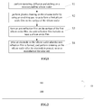
Figure 1 is a schematic flowchart of a method for manufacturing a solar cell according to an embodiment of the invention; and -
Figures 2 ,3 and6 are sectional views of the solar cell during the manufacturing method according to embodiments of the invention. -
Figures 4, 5 and7 are sectional views of the solar cell during the manufacturing method according to examples not being part of the present invention. - As described in the background, in the photovoltaic module manufactured by using the existing solar cell manufacturing processes, the potential induced degradation effect is prone to occur, so the electrical performance parameters of the photovoltaic module, such as FF, Jsc and Voc are deteriorated and will be lower than the design criteria when the photovoltaic module operates under the high negative voltage for a long time.
- The inventor has found that there are mainly two reasons which cause the potential induced degradation effect, one is related to the photovoltaic module system and the other is related to the photovoltaic module.
- As for the photovoltaic module system, it is indicated by the research and the actual operation of the power plant that, in a case that all of the photovoltaic modules between the solar cell module in the middle of the solar cell module array and the negative output terminal of the inverter operate under negative bias, the closer the solar cell module is to the negative output terminal of the inverter, the stronger the potential induced degradation effect is; and in a case that all of the modules between the solar cell module in the middle of the solar cell module array and the positive output terminal of the inverter operate under positive bias, the potential induced degradation effect is not obvious. Whether the solar cell module and the solar cell thereof operate under the positive bias or the negative bias is depended on the grounding mode of the photovoltaic module system and the position of the photovoltaic module in the solar cell module array.
- As for the photovoltaic module, external environmental conditions, such as temperature and humidity, may cause leakage current passages to be formed among the packaging material, the glass backboard, the glass substrate and the packaging frame of the photovoltaic module, and thus the leakage current is formed between the solar cell and the grounding frame. Therefore, the electrical performance parameters of the photovoltaic module, such as the fill factor FF, the short-circuit current Jsc and the open circuit voltage Voc are deteriorated, and thus the electrical performance of the photovoltaic module will be lower than the design criteria.
- The inventor has also found that the method for reducing the potential induced degradation effect of the photovoltaic module in the prior art is mainly to use packaging material with high body resistance and good quality. Although this method can reduced the potential induced degradation effect to some extent, the cost of the photovoltaic module is greatly increased.
- Based on the above-mentioned researches, a method for manufacturing a solar cell of anti potential induced degradation is provided according to the embodiments of the invention. The method for manufacturing the solar cell includes: performing plasma cleaning on a silicon wafer by using an oxidizing gas, so as to form a first silicon oxide film on the surface of the silicon wafer; and
forming an anti-reflection film on the surface of the first silicon oxide film, where the anti-reflection film includes at least a silicon oxide film. - In the technical solution provided by the embodiments of the invention, the good electrical insulation property of the silicon oxide film is utilized. The plasma cleaning is firstly performed on the silicon wafer by using the oxidizing gas, so as to form a compact first silicon oxide film on the surface of the silicon wafer while cleaning the silicon wafer. Then, the anti-reflection film is formed on the surface of the cleaned silicon wafer, i.e., the anti-reflection film is formed on the surface of the first silicon oxide film, where the anti-reflection film includes at least a silicon oxide film. Therefore, the solar cell manufactured by using the manufacturing method according to the embodiments of the invention has a good electrical insulation property with the outside structures such as the packaging material and the glass substrate, so the corresponding photovoltaic module has an anti potential induced degradation effect, which improves the electrical performance of the photovoltaic module operating under the high negative voltage for a long time. Moreover, there is no need for a special packaging material, leading to a low cost. Furthermore, the technical solution is also compatible with the conventional manufacturing processes of the solar cell and thus suitable for large-scale production.
- To make the above objects, features and advantages of the invention more obvious and easy to be understood, specific embodiments of the invention will be illustrated in detail below in conjunction with the drawings.
- More specific details will be set forth in the following descriptions for sufficient understanding of the invention. However, the invention may also be implemented in other ways different from the way described herein, and similar extensions may be made by those skilled in the art without departing from the scope of the invention as defined in the appended claims. Therefore, the invention is not limited to the specific implementations disclosed hereinafter.
- As shown in
Figure 1 , a method for manufacturing a solar cell is provided by an embodiment of the invention, including the following steps. - Step S1: performing texturing, diffusion and etching on a monocrystalline silicon wafer. It should be noted that the monocrystalline silicon wafer may be a P-type monocrystalline silicon wafer or an N-type monocrystalline silicon wafer, and it is not limited in the present invention. In the embodiment of the invention, the method for manufacturing the solar cell provided by the invention is described in detail by using the P-type monocrystalline silicon wafer as the monocrystalline silicon wafer as an example. Thus, in an embodiment of the invention, the performing texturing, diffusion and etching on a monocrystalline silicon wafer includes performing acid texturing, phosphorus diffusion and etching on a P-type monocrystalline silicon wafer.
- Step S2: performing plasma cleaning on the silicon wafer by using an oxidizing gas, so as to form a first oxide layer film on the surface of the silicon wafer.
- After the
monocrystalline silicon wafer 100 is etched, themonocrystalline silicon wafer 100 is cleaned by using an oxidizing gas, so as to form a compact firstsilicon oxide film 101 on the surface of themonocrystalline silicon wafer 100 while removing the impurity on the surface of themonocrystalline silicon wafer 100, as shown inFigure 2 . It should be noted that, in an embodiment of the invention, the oxidizing gas preferably includes at least N2O, that is, the oxidizing gas is preferably N2O or combination gas of NH3 and N2O. However, the invention is not limited thereto, as long as the impurity on the surface of themonocrystalline silicon wafer 100 can be removed and the compact firstsilicon oxide film 101 can be formed on themonocrystalline silicon wafer 100 during the cleaning. Preferably, the plasma cleaning lasts for 30s to 900s, inclusive. - Step S3: placing the cleaned
monocrystalline silicon wafer 10 into a coating apparatus, introducing a reaction gas into the coating apparatus, and forming ananti-reflection film 20 on the surface of the firstsilicon oxide film 101, where the anti-reflection film includes at least a silicon oxide film, as shown inFigure 3 . - In the embodiment of the invention, the
anti-reflection film 20 may be deposited by using a method of PECVD, APCVD or LPCVD, and the invention is not limited thereto. A commonly-used method for coating the anti-reflection film is PECVD, which mainly includes the following steps. The gas for forming the film is introduced into the coating apparatus. The gas for forming the film is ionized into ions under the action of a RF power supply and a large number of reactive groups are generated after multiple collisions. These reactive groups are absorbed onto the surface of the silicon wafer. The absorbed atoms migrate on the surface of the silicon wafer under the action of their owe kinetic energy and the temperature of the surface of the silicon wafer, and stabilize at the lowest energy point. Meanwhile, the atoms of the surface of the silicon wafer continuously get rid of the binding of the surrounding atoms and enter into the plasmas, to achieve dynamic balance. When the atom deposition speed is faster than the atom escape speed, the desired anti-reflection film can be continuously deposited on the surface of the silicon wafer. - Preferably, in the deposition of the anti-reflection film, the silicon oxide film may be deposited by using a method of PECVD, APCVD or LPCVD. The gas for forming the silicon oxide film includes N2O and SiH4, and the gas flow ratio of N2O to SiH4 ranges from 1 to 50:1, inclusive. It should be noted that, in the deposition of the anti-reflection film, the gas for forming the silicon oxide film may further include NH3, and the gas flow ratio is not limited in the invention and may be determined according a specific process requirement. More preferably, the silicon oxide film has a thickness that ranges from 1nm to 150nm, inclusive.
- It should be noted that the
anti-reflection film 20 is a multi-film structure including a silicon oxide film and a silicon nitride film, so as to improve the light absorption rate of the anti-reflection film and thus improve the photoelectric conversion efficiency of the manufactured solar cell. - Preferably, in the deposition of the anti-reflection film, the silicon nitride film may be deposited by using a method of PECVD, APCVD or LPCVD. The gas for forming the silicon nitride film includes NH3 and SiH4, and the gas flow ratio of NH3 to SiH4 ranges from 1 to 30:1, inclusive. More preferably, the silicon nitride film has a thickness that ranges from 10nm to 150nm, inclusive.
- In an example not being part of the present invention, the forming an
anti-reflection film 20 on the surface of the firstsilicon oxide film 101 includes: introducing the gas for forming the silicon oxide film into the coating apparatus, and depositing a uniformsilicon oxide film 200 on the surface of the firstsilicon oxide film 101, so as to form theanti-reflection film 20, as shown inFigure 4 . In a specific example of the embodiment, the gas for forming thesilicon oxide film 200 in theanti-reflection film 20 includes N2O and SiH4, where the gas flow rate of N2O is 2000sccm, and the gas flow rate of SiH4 is 200sccm. More preferably, the depositedsilicon oxide film 200 has a thickness of 70nm and a refractive index of 1.5. - In another example not being part of the present invention, the forming an
anti-reflection film 20 on the surface of the firstsilicon oxide film 101 includes: introducing the gas for forming the silicon oxide film into the coating apparatus, and depositing a uniformsilicon oxide film 201 on the surface of the firstsilicon oxide film 101; and then introducing the gas for forming the silicon nitride film into the coating apparatus, and depositing a uniformsilicon nitride film 202 on the surface of thesilicon oxide film 201, so as to form theanti-reflection film 20, as shown inFigure 5 . - In a specific implementation of said example, the gas for forming the
silicon oxide film 201 in theanti-reflection film 20 includes N2O and SiH4, where the gas flow rate of N2O is 2000sccm, and the gas flow rate of SiH4 is 200sccm. More preferably, the depositedsilicon oxide film 201 has a thickness of 10nm and a refractive index of 1.5. Moreover, the gas for forming thesilicon nitride film 202 in theanti-reflection film 20 includes NH3 and SiH4, where the gas flow rate of NH3 is 6000sccm, and the gas flow rate of SiH4 is 560sccm. More preferably, the depositedsilicon nitride film 202 has a thickness of 70nm and a refractive index of 2.06. - In the embodiment of the present invention, the forming an
anti-reflection film 20 on the surface of the firstsilicon oxide film 101 includes: introducing the gas for forming the silicon nitride film into the coating apparatus, and depositing a uniformsilicon nitride film 202 on the surface of the firstsilicon oxide film 101; then introducing the gas for forming the silicon oxide film into the coating apparatus, and depositing a uniformsilicon oxide film 201 on the surface of thesilicon nitride film 202, so as to form theanti-reflection film 20, as shown inFigure 6 . - In a specific implementation of the embodiment, the gas for forming the
silicon nitride film 202 in the anti-reflection film includes NH3 and SiH4, where the gas flow rate of NH3 is 6000sccm, and the gas flow rate of SiH4 is 600sccm. More preferably, the depositedsilicon nitride film 202 has a thickness of 70 nm and a refractive index of 2.07. Moreover, the gas for forming thesilicon oxide film 201 in the anti-reflection film includes N2O and SiH4, where the gas flow rate of N2O is 2000sccm, and the gas flow rate of SiH4 is 200sccm. More preferably, the depositedsilicon oxide film 201 has a thickness of 10nm and a refractive index of 1.5. - In still another example not being part of the present invention, the forming an
anti-reflection film 20 on the surface of the firstsilicon oxide film 101 includes: introducing the gas for forming the silicon oxide film into the coating apparatus, and depositing a uniformsilicon oxide film 201 on the surface of the firstsilicon oxide film 101; then introducing the gas for forming the silicon nitride film into the coating apparatus, and depositing a uniformsilicon nitride film 202 on the surface of thesilicon oxide film 201; and then introducing again the gas for forming the silicon oxide film into the coating apparatus, and depositing a uniformsilicon oxide film 203 on the surface of thesilicon nitride film 202, so as to form theanti-reflection film 20, as shown inFigure 7 . - In a specific implementation of said example, the gas for forming the
silicon oxide film 201 located on the side of thesilicon nitride film 202 near thesilicon wafer 10 includes N2O and SiH4, where the gas flow rate of N2O is 2000sccm, and the gas flow rate of SiH4 is 200sccm. More preferably, the depositedsilicon oxide film 201 has a thickness of 5nm and a refractive index of 1.5. Moreover, the gas for forming thesilicon nitride film 202 includes NH3 and SiH4, where the gas flow rate of NH3 is 6000sccm, and the gas flow rate of SiH4 is 560sccm. More preferably, the depositedsilicon nitride film 202 has a thickness of 70nm and a refractive index of 2.06. Furthermore, the gas for forming thesilicon oxide film 203 located on the side of thesilicon nitride film 202 far away from thesilicon wafer 10 includes N2O and SiH4, where the gas flow rate of N2O is 2000sccm, and the gas flow rate of SiH4 is 200sccm. More preferably, the depositedsilicon oxide film 203 has a thickness of 10nm and a refractive index of 1.5. - Step S4: printing an electrode on the silicon wafer after the
anti-reflection film 20 is formed, and performing sintering on the silicon wafer after the electrode is printed, so as to manufacture the solar cell. - A solar cell is obtained by using the above-mentioned manufacturing method of the present invention.
- In the method for manufacturing the solar cell provided by the embodiments of the invention, before the anti-reflection film is deposited on the surface of the silicon wafer, the silicon wafer is pre-processed, i.e., the plasma cleaning is performed on the silicon wafer by using an oxidizing gas, so as to form a compact first silicon oxide film on the surface of the silicon wafer while removing the impurity on the surface of the silicon wafer; then the anti-reflection film is formed on the surface of the silicon wafer after the plasma cleaning, i.e., the anti-reflection film is formed on the surface of the first silicon oxide film, where the anti-reflection film includes at least a silicon oxide film. Based on the good electrical insulation property of the silicon oxide film, the solar cell manufactured by using the method is insulated with the packaging material, the glass substrate and the glass backboard. Therefore, even in the case where some charges are accumulated on the surface of the solar cell, there is no leakage current between the solar cell and the grounding frame, so the photovoltaic module including the solar cell has an anti potential induced degradation effect, i.e., the potential induced degradation effect generated when the photovoltaic module operates under the high negative voltage for a long time can be reduced or eliminated, which improves the electrical performance of the photovoltaic module operating under the high negative voltage for a long time. Moreover, there is no need for a special packaging material, leading to a low cost. Furthermore, the technical solution is also compatible with the conventional manufacturing processes of the solar cell and thus suitable for large-scale production.
- The various parts of the present invention are described in a progressive manner, with an emphasis placed on explaining the difference between each other. Hence, the same or similar content of one part may also be suitable for other parts.
- The description of the embodiments herein enables those skilled in the art to implement or use the present invention. Multiple modifications to the embodiments will be apparent to those skilled in the art, and the general principle herein may be implemented in other embodiments without departing from the scope of the present invention as defined in the appended claims. Therefore, the present invention will not be limited to the embodiments described herein.
Claims (9)
- A method for manufacturing a solar cell of reduced potential induced degradation, comprising:performing plasma cleaning on a silicon wafer by using an oxidizing gas, so as to form a first silicon oxide film on the surface of the silicon wafer; andforming an anti-reflection film on the surface of the first silicon oxide film, wherein the anti-reflection film comprises at least a silicon oxide film;wherein the step of forming an anti-reflection film on the surface of the first silicon oxide film comprises:depositing a uniform silicon nitride film on the surface of the first silicon oxide film, and depositing a uniform silicon oxide film on the surface of the silicon nitride film, so as to form the anti-reflection film.
- The method for manufacturing the solar cell of reduced potential induced degradation according to claim 1, wherein the oxidizing gas comprises at least N2O.
- The method for manufacturing the solar cell of reduced potential induced degradation according to claim 2, wherein the plasma cleaning lasts for 30s to 900s, inclusive.
- The method for manufacturing the solar cell of reduced potential induced degradation according to any one of claims 1 to 3, wherein the silicon oxide film in the anti-reflection film is deposited by using a method of PECVD, APCVD or LPCVD.
- The method for manufacturing the solar cell of reduced potential induced degradation according to claim 4, wherein the silicon oxide film in the anti-reflection film is formed by gas comprising N2O and SiH4, and gas flow ratio of N2O to SiH4 ranges from 1 to 50:1, inclusive.
- The method for manufacturing the solar cell of reduced potential induced degradation according to claim 5, wherein the silicon oxide film in the anti-reflection film has a thickness that ranges from 1nm to 150nm, inclusive.
- The method for manufacturing the solar cell of reduced potential induced degradation according to claim 1, wherein the silicon nitride film in the anti-reflection film is deposited by using a method of PECVD, APCVD or LPCVD.
- The method for manufacturing the solar cell of reduced potential induced degradation according to claim 7, wherein the silicon nitride film in the anti-reflection film is form by gas comprising NH3 and SiH4, and gas flow ratio of NH3 to SiH4 ranges from 1 to 30:1, inclusive.
- The method for manufacturing the solar cell of reduced potential induced degradation according to claim 8, wherein the silicon nitride film in the anti-reflection film has a thickness that ranges from 10nm to 150nm, inclusive.
Applications Claiming Priority (1)
| Application Number | Priority Date | Filing Date | Title |
|---|---|---|---|
| CN201310092404.3A CN104064622A (en) | 2013-03-21 | 2013-03-21 | Solar energy battery resisting potential-induced attenuation and manufacture method thereof |
Publications (2)
| Publication Number | Publication Date |
|---|---|
| EP2782146A1 EP2782146A1 (en) | 2014-09-24 |
| EP2782146B1 true EP2782146B1 (en) | 2016-10-12 |
Family
ID=48692341
Family Applications (1)
| Application Number | Title | Priority Date | Filing Date |
|---|---|---|---|
| EP13174068.0A Active EP2782146B1 (en) | 2013-03-21 | 2013-06-27 | Method for manufacturing a solar cell with reduced potential induced degradation |
Country Status (3)
| Country | Link |
|---|---|
| US (1) | US20140283904A1 (en) |
| EP (1) | EP2782146B1 (en) |
| CN (1) | CN104064622A (en) |
Families Citing this family (13)
| Publication number | Priority date | Publication date | Assignee | Title |
|---|---|---|---|---|
| DE102012101456A1 (en) * | 2012-02-23 | 2013-08-29 | Schott Solar Ag | Process for producing a solar cell |
| CN106463548B (en) * | 2014-05-29 | 2018-07-24 | 京瓷株式会社 | Solar cell device and solar cell module |
| CN104319313B (en) * | 2014-10-13 | 2016-03-30 | 天威新能源控股有限公司 | Method for preventing potential induced attenuation of polycrystalline silicon solar cell module |
| CN104393061B (en) * | 2014-11-27 | 2016-06-22 | 浙江昱辉阳光能源江苏有限公司 | A kind of crystal silicon solar energy battery antireflective coating and preparation technology thereof |
| CN104762610A (en) * | 2015-01-16 | 2015-07-08 | 横店集团东磁股份有限公司 | PECVD film coating method |
| CN105355723B (en) * | 2015-12-14 | 2019-12-27 | 内蒙古日月太阳能科技有限责任公司 | Preparation method of silicon dioxide passivation film of crystalline silicon solar cell |
| CN105483832B (en) * | 2015-12-29 | 2018-01-19 | 辛煜 | The crystal silicon surface oxygenation device and its method of a kind of resisting potential induced degradation effect |
| JP6707966B2 (en) * | 2016-04-18 | 2020-06-10 | 日本電気硝子株式会社 | Shading plate |
| CN108091704A (en) * | 2017-12-07 | 2018-05-29 | 青海黄河上游水电开发有限责任公司光伏产业技术分公司 | The photovoltaic module of resisting potential induced degradation |
| CN112531034B (en) * | 2019-08-28 | 2022-10-21 | 泰州隆基乐叶光伏科技有限公司 | Solar cell, solar cell panel and preparation method |
| CN110581183A (en) * | 2019-08-29 | 2019-12-17 | 江苏顺风新能源科技有限公司 | A pure black module monocrystalline PERC cell and its preparation process |
| CN110676347A (en) * | 2019-09-27 | 2020-01-10 | 江苏顺风新能源科技有限公司 | PERC battery production control method for improving yield of black components |
| CN115172522B (en) * | 2022-07-12 | 2023-07-21 | 浙江晶科能源有限公司 | Solar cell, preparation method and photovoltaic module |
Family Cites Families (9)
| Publication number | Priority date | Publication date | Assignee | Title |
|---|---|---|---|---|
| JP4864661B2 (en) * | 2006-11-22 | 2012-02-01 | 東京エレクトロン株式会社 | Solar cell manufacturing method and solar cell manufacturing apparatus |
| US20080179762A1 (en) * | 2007-01-25 | 2008-07-31 | Au Optronics Corporation | Layered structure with laser-induced aggregation silicon nano-dots in a silicon-rich dielectric layer, and applications of the same |
| CN101436616B (en) * | 2008-12-05 | 2010-06-23 | 江阴海润太阳能电力有限公司 | Double-layer reflection-decreasing film for silicon solar cell and preparation method thereof |
| US20100210060A1 (en) * | 2009-02-13 | 2010-08-19 | Peter Borden | Double anneal process for an improved rapid thermal oxide passivated solar cell |
| KR101144810B1 (en) * | 2009-07-06 | 2012-05-11 | 엘지전자 주식회사 | Electrode paste for solar cell, solar cell using the paste, and manufacturing method of the solar cell |
| US20110162706A1 (en) * | 2010-01-04 | 2011-07-07 | Applied Materials, Inc. | Passivated polysilicon emitter solar cell and method for manufacturing the same |
| US9337363B2 (en) * | 2011-05-11 | 2016-05-10 | International Business Machines Corporation | Low resistance, low reflection, and low cost contact grids for photovoltaic cells |
| CN102339871B (en) * | 2011-07-30 | 2013-08-14 | 常州天合光能有限公司 | Positive dielectric film of sandwich structure suitable for RIE (reactive ion etching) texture and manufacturing method thereof |
| US20130220410A1 (en) * | 2011-09-07 | 2013-08-29 | Air Products And Chemicals, Inc. | Precursors for Photovoltaic Passivation |
-
2013
- 2013-03-21 CN CN201310092404.3A patent/CN104064622A/en active Pending
- 2013-06-27 EP EP13174068.0A patent/EP2782146B1/en active Active
- 2013-07-03 US US13/935,131 patent/US20140283904A1/en not_active Abandoned
Also Published As
| Publication number | Publication date |
|---|---|
| CN104064622A (en) | 2014-09-24 |
| US20140283904A1 (en) | 2014-09-25 |
| EP2782146A1 (en) | 2014-09-24 |
Similar Documents
| Publication | Publication Date | Title |
|---|---|---|
| EP2782146A1 (en) | Solar cell with reduced potential induced degradation and manufacturing method thereof | |
| US11996494B2 (en) | Low-cost passivated contact full-back electrode solar cell and preparation method thereof | |
| US7838400B2 (en) | Rapid thermal oxide passivated solar cell with improved junction | |
| US20070137699A1 (en) | Solar cell and method for fabricating solar cell | |
| US20200212230A1 (en) | Leakage pathway layer for solar cell | |
| CN110838536A (en) | Back-contact solar cells with various tunnel junction structures and methods of making the same | |
| CN109494261A (en) | Silica-based solar cell and preparation method, photovoltaic module | |
| EP3371833B1 (en) | Photovoltaic device and method for manufacturing the same | |
| CN114744054A (en) | TOPCon battery and preparation method thereof | |
| CN119698114B (en) | Solar cell and preparation method thereof | |
| EP2538447B1 (en) | Solar cell and method for manufacturing the same | |
| CN106653942A (en) | N-type monocrystalline silicon double-sided cell manufacturing method | |
| CN111599898A (en) | Method for manufacturing crystalline silicon solar cell sheet and crystalline silicon solar cell sheet | |
| TWI390755B (en) | Solar cell manufacturing method | |
| CN102185030A (en) | Preparation method of back contact HIT solar battery based on N-type silicon wafer | |
| CN106449850A (en) | High efficiency silicon-based heterojunction double-sided battery and its preparation method | |
| KR101165915B1 (en) | Method for fabricating solar cell | |
| JP2024547156A (en) | SOLAR CELLS AND METHODS FOR FORMING SAME - Patent application | |
| Radhakrishnan et al. | Module-level cell processing of silicon heterojunction interdigitated back-contacted (SHJ-IBC) solar cells with efficiencies above 22%: Towards all-dry processing | |
| CN202076297U (en) | Back contact HIT solar cell structure based on P-type silicon chip | |
| CN114744077A (en) | Manufacturing method of N-type TBC crystalline silicon solar cell | |
| JP5645734B2 (en) | Solar cell element | |
| CN118630073B (en) | Battery cell | |
| KR20050098472A (en) | Solar cell and fabrication method thereof | |
| CN118522776A (en) | A solar cell and a method for preparing the same, and a photovoltaic module |
Legal Events
| Date | Code | Title | Description |
|---|---|---|---|
| PUAI | Public reference made under article 153(3) epc to a published international application that has entered the european phase |
Free format text: ORIGINAL CODE: 0009012 |
|
| 17P | Request for examination filed |
Effective date: 20130627 |
|
| AK | Designated contracting states |
Kind code of ref document: A1 Designated state(s): AL AT BE BG CH CY CZ DE DK EE ES FI FR GB GR HR HU IE IS IT LI LT LU LV MC MK MT NL NO PL PT RO RS SE SI SK SM TR |
|
| AX | Request for extension of the european patent |
Extension state: BA ME |
|
| RBV | Designated contracting states (corrected) |
Designated state(s): AL AT BE BG CH CY CZ DE DK EE ES FI FR GB GR HR HU IE IS IT LI LT LU LV MC MK MT NL NO PL PT RO RS SE SI SK SM TR |
|
| GRAP | Despatch of communication of intention to grant a patent |
Free format text: ORIGINAL CODE: EPIDOSNIGR1 |
|
| INTG | Intention to grant announced |
Effective date: 20160511 |
|
| GRAS | Grant fee paid |
Free format text: ORIGINAL CODE: EPIDOSNIGR3 |
|
| GRAA | (expected) grant |
Free format text: ORIGINAL CODE: 0009210 |
|
| AK | Designated contracting states |
Kind code of ref document: B1 Designated state(s): AL AT BE BG CH CY CZ DE DK EE ES FI FR GB GR HR HU IE IS IT LI LT LU LV MC MK MT NL NO PL PT RO RS SE SI SK SM TR |
|
| REG | Reference to a national code |
Ref country code: GB Ref legal event code: FG4D |
|
| REG | Reference to a national code |
Ref country code: CH Ref legal event code: EP |
|
| REG | Reference to a national code |
Ref country code: AT Ref legal event code: REF Ref document number: 837190 Country of ref document: AT Kind code of ref document: T Effective date: 20161015 |
|
| REG | Reference to a national code |
Ref country code: IE Ref legal event code: FG4D |
|
| REG | Reference to a national code |
Ref country code: DE Ref legal event code: R096 Ref document number: 602013012638 Country of ref document: DE |
|
| REG | Reference to a national code |
Ref country code: CH Ref legal event code: NV Representative=s name: ISLER AND PEDRAZZINI AG, CH |
|
| REG | Reference to a national code |
Ref country code: NL Ref legal event code: FP |
|
| REG | Reference to a national code |
Ref country code: LT Ref legal event code: MG4D |
|
| PG25 | Lapsed in a contracting state [announced via postgrant information from national office to epo] |
Ref country code: LV Free format text: LAPSE BECAUSE OF FAILURE TO SUBMIT A TRANSLATION OF THE DESCRIPTION OR TO PAY THE FEE WITHIN THE PRESCRIBED TIME-LIMIT Effective date: 20161012 |
|
| REG | Reference to a national code |
Ref country code: AT Ref legal event code: MK05 Ref document number: 837190 Country of ref document: AT Kind code of ref document: T Effective date: 20161012 |
|
| PG25 | Lapsed in a contracting state [announced via postgrant information from national office to epo] |
Ref country code: GR Free format text: LAPSE BECAUSE OF FAILURE TO SUBMIT A TRANSLATION OF THE DESCRIPTION OR TO PAY THE FEE WITHIN THE PRESCRIBED TIME-LIMIT Effective date: 20170113 Ref country code: LT Free format text: LAPSE BECAUSE OF FAILURE TO SUBMIT A TRANSLATION OF THE DESCRIPTION OR TO PAY THE FEE WITHIN THE PRESCRIBED TIME-LIMIT Effective date: 20161012 Ref country code: NO Free format text: LAPSE BECAUSE OF FAILURE TO SUBMIT A TRANSLATION OF THE DESCRIPTION OR TO PAY THE FEE WITHIN THE PRESCRIBED TIME-LIMIT Effective date: 20170112 Ref country code: SE Free format text: LAPSE BECAUSE OF FAILURE TO SUBMIT A TRANSLATION OF THE DESCRIPTION OR TO PAY THE FEE WITHIN THE PRESCRIBED TIME-LIMIT Effective date: 20161012 |
|
| PG25 | Lapsed in a contracting state [announced via postgrant information from national office to epo] |
Ref country code: RS Free format text: LAPSE BECAUSE OF FAILURE TO SUBMIT A TRANSLATION OF THE DESCRIPTION OR TO PAY THE FEE WITHIN THE PRESCRIBED TIME-LIMIT Effective date: 20161012 Ref country code: FI Free format text: LAPSE BECAUSE OF FAILURE TO SUBMIT A TRANSLATION OF THE DESCRIPTION OR TO PAY THE FEE WITHIN THE PRESCRIBED TIME-LIMIT Effective date: 20161012 Ref country code: AT Free format text: LAPSE BECAUSE OF FAILURE TO SUBMIT A TRANSLATION OF THE DESCRIPTION OR TO PAY THE FEE WITHIN THE PRESCRIBED TIME-LIMIT Effective date: 20161012 Ref country code: HR Free format text: LAPSE BECAUSE OF FAILURE TO SUBMIT A TRANSLATION OF THE DESCRIPTION OR TO PAY THE FEE WITHIN THE PRESCRIBED TIME-LIMIT Effective date: 20161012 Ref country code: PL Free format text: LAPSE BECAUSE OF FAILURE TO SUBMIT A TRANSLATION OF THE DESCRIPTION OR TO PAY THE FEE WITHIN THE PRESCRIBED TIME-LIMIT Effective date: 20161012 Ref country code: IS Free format text: LAPSE BECAUSE OF FAILURE TO SUBMIT A TRANSLATION OF THE DESCRIPTION OR TO PAY THE FEE WITHIN THE PRESCRIBED TIME-LIMIT Effective date: 20170212 Ref country code: BE Free format text: LAPSE BECAUSE OF FAILURE TO SUBMIT A TRANSLATION OF THE DESCRIPTION OR TO PAY THE FEE WITHIN THE PRESCRIBED TIME-LIMIT Effective date: 20161012 Ref country code: PT Free format text: LAPSE BECAUSE OF FAILURE TO SUBMIT A TRANSLATION OF THE DESCRIPTION OR TO PAY THE FEE WITHIN THE PRESCRIBED TIME-LIMIT Effective date: 20170213 Ref country code: ES Free format text: LAPSE BECAUSE OF FAILURE TO SUBMIT A TRANSLATION OF THE DESCRIPTION OR TO PAY THE FEE WITHIN THE PRESCRIBED TIME-LIMIT Effective date: 20161012 |
|
| REG | Reference to a national code |
Ref country code: DE Ref legal event code: R097 Ref document number: 602013012638 Country of ref document: DE |
|
| PG25 | Lapsed in a contracting state [announced via postgrant information from national office to epo] |
Ref country code: RO Free format text: LAPSE BECAUSE OF FAILURE TO SUBMIT A TRANSLATION OF THE DESCRIPTION OR TO PAY THE FEE WITHIN THE PRESCRIBED TIME-LIMIT Effective date: 20161012 Ref country code: SK Free format text: LAPSE BECAUSE OF FAILURE TO SUBMIT A TRANSLATION OF THE DESCRIPTION OR TO PAY THE FEE WITHIN THE PRESCRIBED TIME-LIMIT Effective date: 20161012 Ref country code: EE Free format text: LAPSE BECAUSE OF FAILURE TO SUBMIT A TRANSLATION OF THE DESCRIPTION OR TO PAY THE FEE WITHIN THE PRESCRIBED TIME-LIMIT Effective date: 20161012 Ref country code: CZ Free format text: LAPSE BECAUSE OF FAILURE TO SUBMIT A TRANSLATION OF THE DESCRIPTION OR TO PAY THE FEE WITHIN THE PRESCRIBED TIME-LIMIT Effective date: 20161012 Ref country code: DK Free format text: LAPSE BECAUSE OF FAILURE TO SUBMIT A TRANSLATION OF THE DESCRIPTION OR TO PAY THE FEE WITHIN THE PRESCRIBED TIME-LIMIT Effective date: 20161012 |
|
| PLBE | No opposition filed within time limit |
Free format text: ORIGINAL CODE: 0009261 |
|
| STAA | Information on the status of an ep patent application or granted ep patent |
Free format text: STATUS: NO OPPOSITION FILED WITHIN TIME LIMIT |
|
| PG25 | Lapsed in a contracting state [announced via postgrant information from national office to epo] |
Ref country code: SM Free format text: LAPSE BECAUSE OF FAILURE TO SUBMIT A TRANSLATION OF THE DESCRIPTION OR TO PAY THE FEE WITHIN THE PRESCRIBED TIME-LIMIT Effective date: 20161012 Ref country code: BG Free format text: LAPSE BECAUSE OF FAILURE TO SUBMIT A TRANSLATION OF THE DESCRIPTION OR TO PAY THE FEE WITHIN THE PRESCRIBED TIME-LIMIT Effective date: 20170112 Ref country code: IT Free format text: LAPSE BECAUSE OF FAILURE TO SUBMIT A TRANSLATION OF THE DESCRIPTION OR TO PAY THE FEE WITHIN THE PRESCRIBED TIME-LIMIT Effective date: 20161012 |
|
| 26N | No opposition filed |
Effective date: 20170713 |
|
| PG25 | Lapsed in a contracting state [announced via postgrant information from national office to epo] |
Ref country code: SI Free format text: LAPSE BECAUSE OF FAILURE TO SUBMIT A TRANSLATION OF THE DESCRIPTION OR TO PAY THE FEE WITHIN THE PRESCRIBED TIME-LIMIT Effective date: 20161012 |
|
| PG25 | Lapsed in a contracting state [announced via postgrant information from national office to epo] |
Ref country code: MC Free format text: LAPSE BECAUSE OF FAILURE TO SUBMIT A TRANSLATION OF THE DESCRIPTION OR TO PAY THE FEE WITHIN THE PRESCRIBED TIME-LIMIT Effective date: 20161012 |
|
| GBPC | Gb: european patent ceased through non-payment of renewal fee |
Effective date: 20170627 |
|
| REG | Reference to a national code |
Ref country code: FR Ref legal event code: ST Effective date: 20180228 |
|
| REG | Reference to a national code |
Ref country code: IE Ref legal event code: MM4A |
|
| PG25 | Lapsed in a contracting state [announced via postgrant information from national office to epo] |
Ref country code: IE Free format text: LAPSE BECAUSE OF NON-PAYMENT OF DUE FEES Effective date: 20170627 Ref country code: LU Free format text: LAPSE BECAUSE OF NON-PAYMENT OF DUE FEES Effective date: 20170627 Ref country code: GB Free format text: LAPSE BECAUSE OF NON-PAYMENT OF DUE FEES Effective date: 20170627 |
|
| PG25 | Lapsed in a contracting state [announced via postgrant information from national office to epo] |
Ref country code: FR Free format text: LAPSE BECAUSE OF NON-PAYMENT OF DUE FEES Effective date: 20170630 |
|
| PG25 | Lapsed in a contracting state [announced via postgrant information from national office to epo] |
Ref country code: MT Free format text: LAPSE BECAUSE OF NON-PAYMENT OF DUE FEES Effective date: 20170627 |
|
| PG25 | Lapsed in a contracting state [announced via postgrant information from national office to epo] |
Ref country code: HU Free format text: LAPSE BECAUSE OF FAILURE TO SUBMIT A TRANSLATION OF THE DESCRIPTION OR TO PAY THE FEE WITHIN THE PRESCRIBED TIME-LIMIT; INVALID AB INITIO Effective date: 20130627 |
|
| PG25 | Lapsed in a contracting state [announced via postgrant information from national office to epo] |
Ref country code: CY Free format text: LAPSE BECAUSE OF FAILURE TO SUBMIT A TRANSLATION OF THE DESCRIPTION OR TO PAY THE FEE WITHIN THE PRESCRIBED TIME-LIMIT Effective date: 20161012 |
|
| PG25 | Lapsed in a contracting state [announced via postgrant information from national office to epo] |
Ref country code: MK Free format text: LAPSE BECAUSE OF FAILURE TO SUBMIT A TRANSLATION OF THE DESCRIPTION OR TO PAY THE FEE WITHIN THE PRESCRIBED TIME-LIMIT Effective date: 20161012 |
|
| PG25 | Lapsed in a contracting state [announced via postgrant information from national office to epo] |
Ref country code: TR Free format text: LAPSE BECAUSE OF FAILURE TO SUBMIT A TRANSLATION OF THE DESCRIPTION OR TO PAY THE FEE WITHIN THE PRESCRIBED TIME-LIMIT Effective date: 20161012 |
|
| PG25 | Lapsed in a contracting state [announced via postgrant information from national office to epo] |
Ref country code: AL Free format text: LAPSE BECAUSE OF FAILURE TO SUBMIT A TRANSLATION OF THE DESCRIPTION OR TO PAY THE FEE WITHIN THE PRESCRIBED TIME-LIMIT Effective date: 20161012 |
|
| REG | Reference to a national code |
Ref country code: DE Ref legal event code: R079 Ref document number: 602013012638 Country of ref document: DE Free format text: PREVIOUS MAIN CLASS: H01L0031180000 Ipc: H10F0071000000 |
|
| PGFP | Annual fee paid to national office [announced via postgrant information from national office to epo] |
Ref country code: DE Payment date: 20250618 Year of fee payment: 13 |
|
| PGFP | Annual fee paid to national office [announced via postgrant information from national office to epo] |
Ref country code: NL Payment date: 20250618 Year of fee payment: 13 |
|
| PGFP | Annual fee paid to national office [announced via postgrant information from national office to epo] |
Ref country code: CH Payment date: 20250701 Year of fee payment: 13 |