EP2779461B1 - Verfahren und Vorrichtung zur Verbesserung der Konvergenzzeit in korrelationsbasierten Algorithmen - Google Patents
Verfahren und Vorrichtung zur Verbesserung der Konvergenzzeit in korrelationsbasierten Algorithmen Download PDFInfo
- Publication number
- EP2779461B1 EP2779461B1 EP14157886.4A EP14157886A EP2779461B1 EP 2779461 B1 EP2779461 B1 EP 2779461B1 EP 14157886 A EP14157886 A EP 14157886A EP 2779461 B1 EP2779461 B1 EP 2779461B1
- Authority
- EP
- European Patent Office
- Prior art keywords
- stages
- stage
- adc
- signals
- input
- Prior art date
- Legal status (The legal status is an assumption and is not a legal conclusion. Google has not performed a legal analysis and makes no representation as to the accuracy of the status listed.)
- Active
Links
- 238000004422 calculation algorithm Methods 0.000 title claims description 23
- 238000000034 method Methods 0.000 title claims description 20
- 238000002347 injection Methods 0.000 description 7
- 239000007924 injection Substances 0.000 description 7
- 238000010586 diagram Methods 0.000 description 6
- 230000000875 corresponding effect Effects 0.000 description 3
- 230000006870 function Effects 0.000 description 3
- 108010076504 Protein Sorting Signals Proteins 0.000 description 2
- 238000006243 chemical reaction Methods 0.000 description 2
- 238000003491 array Methods 0.000 description 1
- 238000004364 calculation method Methods 0.000 description 1
- 239000003990 capacitor Substances 0.000 description 1
- 230000002596 correlated effect Effects 0.000 description 1
- 230000003111 delayed effect Effects 0.000 description 1
- 238000009795 derivation Methods 0.000 description 1
- 230000000694 effects Effects 0.000 description 1
- 238000004519 manufacturing process Methods 0.000 description 1
- 230000000135 prohibitive effect Effects 0.000 description 1
- 238000005070 sampling Methods 0.000 description 1
- 230000001960 triggered effect Effects 0.000 description 1
Images


Classifications
-
- H—ELECTRICITY
- H03—ELECTRONIC CIRCUITRY
- H03M—CODING; DECODING; CODE CONVERSION IN GENERAL
- H03M1/00—Analogue/digital conversion; Digital/analogue conversion
- H03M1/10—Calibration or testing
- H03M1/1071—Measuring or testing
-
- H—ELECTRICITY
- H03—ELECTRONIC CIRCUITRY
- H03M—CODING; DECODING; CODE CONVERSION IN GENERAL
- H03M1/00—Analogue/digital conversion; Digital/analogue conversion
- H03M1/06—Continuously compensating for, or preventing, undesired influence of physical parameters
- H03M1/0617—Continuously compensating for, or preventing, undesired influence of physical parameters characterised by the use of methods or means not specific to a particular type of detrimental influence
- H03M1/0634—Continuously compensating for, or preventing, undesired influence of physical parameters characterised by the use of methods or means not specific to a particular type of detrimental influence by averaging out the errors, e.g. using sliding scale
- H03M1/0636—Continuously compensating for, or preventing, undesired influence of physical parameters characterised by the use of methods or means not specific to a particular type of detrimental influence by averaging out the errors, e.g. using sliding scale in the amplitude domain
- H03M1/0639—Continuously compensating for, or preventing, undesired influence of physical parameters characterised by the use of methods or means not specific to a particular type of detrimental influence by averaging out the errors, e.g. using sliding scale in the amplitude domain using dither, e.g. using triangular or sawtooth waveforms
- H03M1/0641—Continuously compensating for, or preventing, undesired influence of physical parameters characterised by the use of methods or means not specific to a particular type of detrimental influence by averaging out the errors, e.g. using sliding scale in the amplitude domain using dither, e.g. using triangular or sawtooth waveforms the dither being a random signal
-
- H—ELECTRICITY
- H03—ELECTRONIC CIRCUITRY
- H03M—CODING; DECODING; CODE CONVERSION IN GENERAL
- H03M1/00—Analogue/digital conversion; Digital/analogue conversion
-
- H—ELECTRICITY
- H03—ELECTRONIC CIRCUITRY
- H03M—CODING; DECODING; CODE CONVERSION IN GENERAL
- H03M1/00—Analogue/digital conversion; Digital/analogue conversion
- H03M1/06—Continuously compensating for, or preventing, undesired influence of physical parameters
- H03M1/0617—Continuously compensating for, or preventing, undesired influence of physical parameters characterised by the use of methods or means not specific to a particular type of detrimental influence
- H03M1/0675—Continuously compensating for, or preventing, undesired influence of physical parameters characterised by the use of methods or means not specific to a particular type of detrimental influence using redundancy
- H03M1/069—Continuously compensating for, or preventing, undesired influence of physical parameters characterised by the use of methods or means not specific to a particular type of detrimental influence using redundancy by range overlap between successive stages or steps
- H03M1/0695—Continuously compensating for, or preventing, undesired influence of physical parameters characterised by the use of methods or means not specific to a particular type of detrimental influence using redundancy by range overlap between successive stages or steps using less than the maximum number of output states per stage or step, e.g. 1.5 per stage or less than 1.5 bit per stage type
-
- H—ELECTRICITY
- H03—ELECTRONIC CIRCUITRY
- H03M—CODING; DECODING; CODE CONVERSION IN GENERAL
- H03M1/00—Analogue/digital conversion; Digital/analogue conversion
- H03M1/10—Calibration or testing
- H03M1/1009—Calibration
-
- H—ELECTRICITY
- H03—ELECTRONIC CIRCUITRY
- H03M—CODING; DECODING; CODE CONVERSION IN GENERAL
- H03M1/00—Analogue/digital conversion; Digital/analogue conversion
- H03M1/12—Analogue/digital converters
-
- H—ELECTRICITY
- H03—ELECTRONIC CIRCUITRY
- H03M—CODING; DECODING; CODE CONVERSION IN GENERAL
- H03M1/00—Analogue/digital conversion; Digital/analogue conversion
- H03M1/12—Analogue/digital converters
- H03M1/14—Conversion in steps with each step involving the same or a different conversion means and delivering more than one bit
- H03M1/16—Conversion in steps with each step involving the same or a different conversion means and delivering more than one bit with scale factor modification, i.e. by changing the amplification between the steps
- H03M1/164—Conversion in steps with each step involving the same or a different conversion means and delivering more than one bit with scale factor modification, i.e. by changing the amplification between the steps the steps being performed sequentially in series-connected stages
-
- H—ELECTRICITY
- H03—ELECTRONIC CIRCUITRY
- H03M—CODING; DECODING; CODE CONVERSION IN GENERAL
- H03M1/00—Analogue/digital conversion; Digital/analogue conversion
- H03M1/12—Analogue/digital converters
- H03M1/34—Analogue value compared with reference values
- H03M1/38—Analogue value compared with reference values sequentially only, e.g. successive approximation type
- H03M1/44—Sequential comparisons in series-connected stages with change in value of analogue signal
Definitions
- Random signal sequences are sometimes injected into circuits.
- the randomness of the sequences may refer to the amplitude of the signals in the sequences, which may, for example, randomly vary between a set of discrete, predefined values. These sequences may be uncorrelated with the input signals to the circuits, i.e., the useful signals. The sequences may also be uncorrelated with each other.
- the sequences can be used for a variety of purposes, which are known in the art. For example, random sequences may be used to calibrate one or more stages of a pipelined analog-to-digital converter (ADC), e.g., to reduce a degree of mismatch between the devices in the stages or correct for non-linearity errors.
- ADC analog-to-digital converter
- Random sequences may also be used for dithering the input signal or for performing other types of calibrations. For convenience, these random or pseudo-random sequences will be referred to herein as "dither" signals, even though they may not be used to perform dithering in the traditional sense.
- a pipelined ADC it may be desirable to remove the dither signals from the output of the ADC. This may be difficult because dither injected into one stage may propagate through subsequent stages, thereby influencing the signals output from one stage to the next, and may ultimately influence the overall output as well. Dither signals also experience the same gain effects as the input signals applied to the stages into which the dither is injected. Therefore, removal of the dither signals is not as straightforward as simply subtracting the dither injected into a stage from the output of that stage.
- One method of removing dither signals from the output of the ADC is to correlate them out where they are used, by taking advantage of the lack of correlation between the dither signals. For example, if one sequence is used to calibrate stage 1 in a pipelined ADC, while other sequences are used to calibrate other stages, and/or to dither the pipeline, a correlation algorithm such as a Least Means Square (LMS) algorithm may be applied to correlate the overall output of the ADC with the sequence injected into stage 1 to determine a degree of correlation between the injected sequence and the overall output (which includes all the sequences). In a similar fashion, the degree of correlation between the sequences injected into other stages and the overall output may be determined.
- LMS Least Means Square
- each stage is then adjusted based on the degree of correlation for the respective stage so that, over time, the error attributed to the sequences is gradually reduced so that the sequences will average out to zero, while the intended sequence, i.e., the useful signal corresponding to the analog input of the ADC, remains.
- the convergence time of the correlation algorithm can be very long, even in the absence of any input signal, e.g., when the input is disconnected and only the random sequences are injected. This leads to long start-up times and long production test times, which can be prohibitive.
- the invention concerns a method of calibrating a pipelined analog to digital converter according to claim 1 and a corresponding pipelined analog to digital converter according to claim 6.
- Example embodiments of the present invention relate to improving the convergence time in correlation-based algorithms that are applied to random or pseudorandom signal sequences injected simultaneously into an ADC.
- the convergence time may be reduced by reconstructing an estimate of the dither signals and subtracting them out, before applying the correlation algorithm on the desired sequence. This substantially reduces the "energy" of the undesired sequences and hence improves the convergence time significantly.
- a substantial portion of the sequences may be removed, e.g., using subtraction, prior to applying the correlation algorithm.
- Example embodiments are described in connection with a pipelined ADC.
- Fig. 1 is a block diagram of a multi-stage pipelined ADC 100.
- An analog signal Vin is input to a first stage 10 of the ADC.
- a comparison between the input and a set of reference voltages may be performed by a bank of comparators, resulting in a coarse digital estimate of the input, which is output to an output circuit 18 to which all the stages are connected.
- the coarse estimate is also accurately converted into a voltage and subtracted from the input with the aid of a digital-to-analog converter (DAC) and subtraction circuitry.
- DAC digital-to-analog converter
- the resulting analog residue signal is gained-up and provided as input to the next stage. This is repeated through any number of additional stages (e.g., stages 12 and 14) until the end of the pipeline (the final stage 16) is reached.
- the number of stages can be selected based on a desired resolution of the ADC.
- Fig. 1 includes a blow-up view showing various components of the stage 10.
- Each of the remaining stages 12 / 14 / 16 may include similar components, except the final stage 16 may not include a digital-to-analog converter (DAC) or a subtraction unit.
- the input Vin is passed to a flash unit 10a, which performs an analog-to-digital conversion of Vin to generate a digital value FD1.
- Vin may be applied to a set of comparators in the flash unit 10a.
- any number of comparators may be triggered to generate a digital approximation of Vin, since each comparator may have a different triggering threshold.
- FD1 is input to a DAC 10b, which converts FD1 into an analog signal.
- the analog version of FD1 may then be subtracted from Vin by a subtraction unit 10c, before being gained-up by a gain unit 10d and passed to the next stage (e.g., stage 12) as an analog residue signal R1. This process may be repeated until the end of the pipeline is reached.
- the overall output of the ADC is then generated by an output circuit 18, which combines the digital output of each stage (e.g., FD1, FD2 ... FDN) into a single digital output (ADC Output). Since the stages operate in a pipelined fashion, the FD signals from each stage are appropriately delayed (e.g., by the output circuit 18) so that all the output signals from the same sample instant are time-aligned.
- the output circuit 18 may then generate the ADC Output by combining the time-aligned signals, e.g., as a digital summation of the time-aligned signals.
- Fig. 2 is a block diagram of a multi-stage pipelined ADC 200 with dither injection.
- the components may be identical to those discussed in connection with the ADC 100 of Fig. 1 , except that each stage may additionally include a hardware arrangement for injecting dither into the stage.
- this arrangement is shown as an addition unit 10e that sums the digital output of the flash 10a with a dither signal Dithl.
- the dither may be injected directly into the DAC 10b.
- the hardware arrangement for combining the dither with an existing signal in the stage need not be an addition unit, but may, for example, utilize existing components such as capacitors in the DAC 10b.
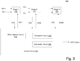
- Fig. 3 is a block diagram of a system 300 according to an example embodiment of the present invention.
- the system includes a plurality of pipelined stages 100 / 110 / 120 and a control circuit 200.
- the stages 100 / 110 / 120 may be similar in structure to the stages previously described in connection with Figs. 1 and 2 .
- the ADC in the system 300 may operate on a differential input. For this reason, two input signals Vin+ and Vin- are shown.
- the control circuit 200 may be analogous to the output circuit 18 in Figs. 1 and 2 in that the control circuit 200 may be configured to combine the digital outputs from the flashes in each stage to form the overall output. This is illustrated in Fig. 3 by presence of the ADC Output signal at an output of the control circuit 200. However, in alternative embodiments, the control circuit 200 may be used in conjunction with a separate output circuit that performs the combining. Similarly, each of the block components in the control circuit 200 may be implemented as a separate device.
- the control circuit 200 may include a dither injection circuit, a correlation circuit 220 and a subtraction circuit 230.
- the dither injection circuit 210 includes a circuit arrangement for generating and injecting dither into each stage. This circuit arrangement may determine the values of the dither signals, e.g., by implementing a function that randomly selects a value from a set of discrete, predefined values.
- the correlation circuit 220 may implement a correlation algorithm such as LMS to correlate the overall output of the ADC, i.e., ADC Output, to each of the dither signals (Dithl, Dith2, Dith3, etc.).
- a correlation algorithm such as LMS to correlate the overall output of the ADC, i.e., ADC Output, to each of the dither signals (Dithl, Dith2, Dith3, etc.).
- the subtraction circuit 230 may implement a method for improving the convergence time of the correlation algorithm of the correlation circuit 220. An example embodiment of this method will be described with reference to Fig. 4 .
- the subtraction circuit 230 may include a processor that performs calculations to estimate the ideal amplitudes of the unwanted portions of the residue signals, which unwanted portions correspond to the dither signals, and then subtracts the unwanted portions, which may be considered as a form of noise, before the correlation algorithm is executed.
- the estimates may be subject to non-idealities in the pipeline, to which non-idealities the input Vin is also subject. However, for purposes of improving the convergence time, the estimates produced by the subtraction circuit 230 are reasonably close enough that the amplitude of the dither signals may be reduced by at least an order of magnitude, thereby resulting in a substantial reduction in convergence time.
- the subtraction circuit 230 may reconstruct an estimate of the dither residue (that portion of the stage residue which is attributed to the dither signal) as it appears at the stage of interest, then subtract the estimate from the stage residue, leaving only the intended residue as input to the next stage (the stage of interest).
- the subtraction circuit 230 may obtain the flash output of each stage (e.g., FD1, FD2, FD3, etc.). Each of these flash outputs may be a multi-bit signal, with the number of bits being variable among the stages.
- the control circuit 200 may temporarily disconnect the input Vin so that the input is not reflected in the flash outputs. The input may alternatively be manually disconnected. However, the input may be reconnected after the estimates are calculated.
- the dither signals may continue to be applied as when the input was disconnected, but because of the subtraction only the dither that is relevant to each particular stage is applied to that stage, e.g., subtracting the noise attributed to the dither injected into stages 1 and 2 from the residue of stage 3 leaves only the dither injected into stage 3 as the relevant dither in stage 3.
- the dither in stage 3 After the dither in stage 3 has performed its intended function, it can be correlated out in the traditional manner using the LMS algorithm or another correlation algorithm.
- the example embodiments of the present invention may be used in connection with background based calibration techniques, i.e., calibrations performed while the ADC is actively performing conversion of input.
- the subtraction circuit 230 may also obtain the values of the dither signals (e.g., Dith1, Dith2, Dith3, etc.) as well as the processing characteristics of the stages, e.g., the gain values for each stage (G1, G2 and G3, etc.). These gain values correspond to the gain of the amplifier 10d in Fig. 2 .
- Each of the values is obtainable because it is known beforehand, either from design specifications (e.g., gain may be a design specification) or from another circuit component (e.g., dither may be determined by the dither injection circuit 210).
- the residues of the three stages are R1, R2 and R3, respectively; the flash bits are FD1, FD2 and FD3, respectively; and the dithers injected into these stages are Dith1, Dith2 and Dith3, respectively.
- the residue is composed of Dith3, e.g., the stage 3 calibration signal.
- the residue is also composed of "noise" components attributed to Dithl and Dith2, the dither injected into the preceding stages. Therefore, the Dithl and Dith2 components should be removed in order for the correlation algorithm to converge with respect to stage 3.
- N3 is the noise attributed to the dither signals of stage 1 and stage 2 as presented at the output of stage 3.
- the following equations show the derivation of the formula for the stage 3 noise:
- N 3 Dith 2 + Dith 1 ⁇ G 1 ⁇ FD 2 ⁇ G 2 ⁇ FD 3 ⁇ G 3
- N 3 Dith 1 ⁇ G 1 ⁇ G 2 ⁇ G 3 + Dith 2 ⁇ FD 2 ⁇ G 2 ⁇ G 3 ⁇ FD 3 ⁇ G 3
- the above equations show that it is possible to estimate the noise based in part on the flash bits of the relevant stages.
- the subtraction circuit 230 can then subtract this noise value from the residue using analog or digital techniques.
- N3 may be digitally subtracted using a subtraction unit connected to R3.
- Fig. 4 is a flowchart of a method 400 according to an example embodiment of the present invention.
- the method 400 may be performed on a processor of a computer, e.g., the control device 200 or the subtraction circuit 230.
- the input is disconnected and the digital values, i.e., the flash bits, generated by each stage in which dither is injected are obtained along with their corresponding dither values.
- the gain values may also be obtained and may be read from a memory.
- the noise component of the residue signal is calculated as a function of the dither values, the gain values and the flash bits, as discussed above.
- the noise may be calculated for each dither-injected stage after the first stage.
- the noise is subtracted from the residue of each respective stage.
- the input is reconnected and the correlation algorithm may be executed.
- the method 400 may be repeated to subtract noise from any number of sampling cycles, thereby removing the noise attributed to the dither injected in each of these cycles. As a result, the convergence time of the correlation algorithm is reduced.
- An example embodiment of the present invention is directed to one or more processors, which may be implemented using any conventional processing circuit and device or combination thereof, e.g., Personal Computer Central Processing Unit(s), Microprocessors, Field Programmable Gate Arrays (FPGAs), etc., to execute instructions provided, e.g., on a hardware computer-readable medium including any conventional memory device, to perform any of the methods described herein, alone or in combination.
- processors may be implemented using any conventional processing circuit and device or combination thereof, e.g., Personal Computer Central Processing Unit(s), Microprocessors, Field Programmable Gate Arrays (FPGAs), etc.
Landscapes
- Engineering & Computer Science (AREA)
- Theoretical Computer Science (AREA)
- Analogue/Digital Conversion (AREA)
- Complex Calculations (AREA)
Claims (10)
- Verfahren zum Kalibrieren eines im Pipelinesystem verarbeiteten Analog-DigitalWandlers, ADC, umfassend einen analogen Signaleingang und mehrere Stufen, wobei jede Stufe des im Pipelinesystem verarbeiteten ADC einen digitalen Ausgang (FD1, FD2, ... FDN) umfasst, wobei das Verfahren umfasst:
Verwenden eines Prozessors (200) des im Pipelinesystem verarbeiteten ADC (300) zur Durchführung der Kalibrierung durch:Trennen einer Eingangsstufe des im Pipelinesystem verarbeiteten ADC vom analogen Signaleingang;Einspeisen von Zufallssignalen (Dith1, Dith2, Dith3) in mindestens einige Stufen der mehreren Stufen (100, 110, 120) des im Pipelinesystem verarbeiteten ADC;Erhalten digitaler Werte, die als Reaktion auf die Zufallssignale erzeugt werden, wobei die digitalen Werte an den jeweiligen digitalen Ausgängen (FD1, FD2, FD3) der mindestens einigen Stufen erhalten werden; gekennzeichnet durchBerechnen einer Rauschkomponente eines jeweiligen Restsignals der mindestens einen Stufe als Funktion der digitalen Werte und der Werte der Zufallssignale für mindestens eine Stufe (120) der mindestens einigen Stufen, die einer ersten der mindestens einigen Stufen (110, 120) folgt, wobei die Rauschkomponente durch das Zufallssignal oder die Zufallssignale verursacht wird, die in die Stufe oder Stufen der mindestens einigen Stufen, die der mindestens einen Stufe vorausgeht/vorausgehen, eingespeist werden; undSubtrahieren der Rauschkomponenten von ihren jeweiligen Restsignalen. - Verfahren nach Anspruch 1, ferner Folgendes umfassend:
Anwenden eines Korrelationsalgorithmus, der die Zufallssignale und eine Gesamtausgabe des ADC als Eingaben verwendet, wobei der Korrelationsalgorithmus nach dem Subtrahieren angewendet wird. - Verfahren nach Anspruch 2, wobei der Korrelationsalgorithmus angewandt wird, um die Zufallssignale aus dem gesamten Ausgangssignal des ADC (300) zu entfernen.
- Verfahren nach einem der vorhergehenden Ansprüche, wobei die Eingangsstufe nach dem Subtrahieren wieder an den analogen Signaleingang angeschlossen wird.
- Verfahren nach einem der vorhergehenden Ansprüche, wobei die Rauschkomponenten zusätzlich als eine Funktion von Verstärkungswerten berechnet werden, die die Verstärkungskennlinien der Stufen anzeigen.
- Im Pipelinesystem verarbeiteter Analog-Digital-Wandler, ADC, umfassend einen analogen Signaleingang und mehrere Stufen, wobei jede Stufe des im Pipelinesystem verarbeiteten ADC einen digitalen Ausgang (FD1, FD2, ... FDN) umfasst, wobei der ADC ferner umfasst:
einen Prozessor (200), der für Folgendes konfiguriert ist:Trennen einer Eingangsstufe des im Pipelinesystem verarbeiteten ADC vom analogen Signaleingang;Einspeisen von Zufallssignalen (Dith1, Dith2, Dith3) in mindestens einige Stufen der mehreren Stufen (100, 110, 120) des im Pipelinesystem verarbeiteten ADC,zum Erhalten digitaler Werte, die als Reaktion auf die Zufallssignale erzeugt werden, wobei die digitalen Werte an den jeweiligen digitalen Ausgängen (FD1, FD2, FD3) der mindestens einigen Stufen erhalten werden;dadurch gekennzeichnet, dass der Prozessor ferner konfiguriert ist, um für mindestens eine Stufe (120) der mindestens einigen Stufen, die einer ersten der mindestens einigen Stufen (110, 120) folgt, eine Rauschkomponente eines Restsignals der mindestens einen Stufe als Funktion der digitalen Werte und der Werte der Zufallssignale zu berechnen, wobei die Rauschkomponente durch das Zufallssignal oder die Zufallssignale verursacht wird, die in die Stufe oder Stufen der mindestens einigen Stufen, die der mindestens einen Stufe vorausgeht oder vorausgehen, eingespeist werden; unddie Rauschkomponenten von ihren jeweiligen Restsignalen subtrahiert werden. - Vorrichtung nach Anspruch 6, wobei der Prozessor konfiguriert ist, um einen Korrelationsalgorithmus anzuwenden, der die Zufallssignale und ein Gesamtausgangssignal des ADC als Eingang verwendet, wobei der Korrelationsalgorithmus nach dem Subtrahieren angewandt wird.
- Vorrichtung nach Anspruch 7, wobei der Prozessor konfiguriert ist, um den Korrelationsalgorithmus anzuwenden, um die Zufallssignale aus dem Gesamtausgangssignal des ADC (300) zu entfernen.
- Vorrichtung nach einem der Ansprüche 6 bis 8, wobei der Prozessor (200) konfiguriert ist, um nach dem Subtrahieren die Eingangsstufe wieder mit dem analogen Signaleingang zu verbinden.
- Vorrichtung nach einem der Ansprüche 6 bis 9, wobei der Prozessor (200) konfiguriert ist, zusätzlich die Rauschkomponenten als eine Funktion von Verstärkungswerten, die die Verstärkungskennlinien der Stufen anzeigen, zu berechnen.
Applications Claiming Priority (2)
| Application Number | Priority Date | Filing Date | Title |
|---|---|---|---|
| US201361791279P | 2013-03-15 | 2013-03-15 | |
| US13/897,604 US8836558B1 (en) | 2013-03-15 | 2013-05-20 | Method and device for improving convergence time in correlation-based algorithms |
Publications (3)
| Publication Number | Publication Date |
|---|---|
| EP2779461A2 EP2779461A2 (de) | 2014-09-17 |
| EP2779461A3 EP2779461A3 (de) | 2016-08-10 |
| EP2779461B1 true EP2779461B1 (de) | 2020-06-24 |
Family
ID=50389784
Family Applications (1)
| Application Number | Title | Priority Date | Filing Date |
|---|---|---|---|
| EP14157886.4A Active EP2779461B1 (de) | 2013-03-15 | 2014-03-05 | Verfahren und Vorrichtung zur Verbesserung der Konvergenzzeit in korrelationsbasierten Algorithmen |
Country Status (3)
| Country | Link |
|---|---|
| US (1) | US8836558B1 (de) |
| EP (1) | EP2779461B1 (de) |
| CN (1) | CN104135287B (de) |
Families Citing this family (4)
| Publication number | Priority date | Publication date | Assignee | Title |
|---|---|---|---|---|
| US9154146B1 (en) * | 2014-06-03 | 2015-10-06 | The Board Of Regents, The University Of Texas System | Dynamic offset injection for CMOS ADC front-end linearization |
| US10547319B2 (en) * | 2017-11-01 | 2020-01-28 | Analog Devices, Inc. | Background calibration of reference, DAC, and quantization non-linearity in ADCS |
| DE102018126606B4 (de) | 2017-11-01 | 2022-11-24 | Analog Devices, Inc. | Hintergrundkalibration von Referenz-, DAC- und Quantisierungs-Nichtlinearität in ADCs |
| CN110336561B (zh) * | 2019-07-05 | 2021-02-05 | 中国电子科技集团公司第二十四研究所 | 一种流水线型模数转换器及其输出校正方法 |
Family Cites Families (5)
| Publication number | Priority date | Publication date | Assignee | Title |
|---|---|---|---|---|
| DE602006007497D1 (de) * | 2006-02-27 | 2009-08-06 | St Microelectronics Srl | Mehrstufiger analog/digital-umsetzer und verfahren zum kalibrieren des umsetzers |
| US7595748B2 (en) * | 2007-07-23 | 2009-09-29 | Mediatek Inc. | Method of gain error calibration in a pipelined analog-to-digital converter or a cyclic analog-to-digital converter |
| US8451152B2 (en) * | 2011-02-22 | 2013-05-28 | Texas Instruments Incorporated | Pipelined ADC inter-stage error calibration |
| US8791844B2 (en) * | 2011-06-09 | 2014-07-29 | Microchip Technology Incorporated | Modified dynamic element matching for reduced latency in a pipeline analog to digital converter |
| US8493259B2 (en) * | 2011-12-06 | 2013-07-23 | Taiwan Semiconductor Manufacturing Co., Ltd. | Pipeline analog-to-digital converter |
-
2013
- 2013-05-20 US US13/897,604 patent/US8836558B1/en active Active
-
2014
- 2014-03-05 EP EP14157886.4A patent/EP2779461B1/de active Active
- 2014-03-14 CN CN201410093858.7A patent/CN104135287B/zh active Active
Non-Patent Citations (1)
| Title |
|---|
| None * |
Also Published As
| Publication number | Publication date |
|---|---|
| EP2779461A3 (de) | 2016-08-10 |
| US8836558B1 (en) | 2014-09-16 |
| CN104135287A (zh) | 2014-11-05 |
| US20140266844A1 (en) | 2014-09-18 |
| CN104135287B (zh) | 2018-07-03 |
| EP2779461A2 (de) | 2014-09-17 |
Similar Documents
| Publication | Publication Date | Title |
|---|---|---|
| US10103753B1 (en) | Error correcting analog-to-digital converters | |
| CN109756226B (zh) | 参考dac的背景校准和adc中的量化非线性 | |
| JP5875697B2 (ja) | インターリーブされたadcにおけるタイミング、利得および帯域幅ミスマッチの較正 | |
| EP2850732B1 (de) | Kalibrierungstiming, verstärkung und bandbreitenfehlanpassung in verschachtelten adcs mit einspeisung von zufallsimpulsen | |
| CN104067521B (zh) | 用于减低流水线式模数转换器中的级间增益误差和非线性的基于关联的背景校准 | |
| US8471740B2 (en) | Reducing the effect of non-linear kick-back in switched capacitor networks | |
| US20020041248A1 (en) | Digital cancellation of D/A converter noise in pipelined A/D converters | |
| EP2779461B1 (de) | Verfahren und Vorrichtung zur Verbesserung der Konvergenzzeit in korrelationsbasierten Algorithmen | |
| CN103703686B (zh) | 用于流水线模/数转换器中的减少的等待时间的经修改动态元件匹配 | |
| US10771078B2 (en) | Comparator offset calibration system and analog-to-digital converter with comparator offset calibration | |
| Le Duc et al. | A fully digital background calibration of timing skew in undersampling TI-ADC | |
| EP1366571B1 (de) | Kalibrationstestsequenz einfügung für a/d-umsetzer | |
| TW201240354A (en) | Test apparatus and test method of analog to digital converter | |
| TWI513196B (zh) | 信號發生裝置及信號發生方法 | |
| KR20120122972A (ko) | 2?채널 타임?인터리브된 아날로그?디지털 컨버터에서의 샘플?타임 미스매치 에러 캘리브레이션에 대한 그래디언트?기반 접근 | |
| Salib et al. | A low-complexity correlation-based time skew estimation technique for time-interleaved SAR ADCs | |
| US20130154860A1 (en) | Use of logic circuit embedded into comparator for foreground offset cancellation | |
| US9344301B2 (en) | Acquisition device with multistage digital equalization | |
| EP3534540B1 (de) | Hintergrundkalibrierung von zufälligen schnittfehlern in datenwandlern | |
| CN105720978B (zh) | 流水线adc的后台校准方法及电路 | |
| JP5795827B2 (ja) | インターリーブドおよびマルチチャネルadcにおけるチャネル間結合を低減するための方法ならびに装置 | |
| Zhu et al. | Digital background calibration for pipelined ADC and implementation of Full FPGA verification platform | |
| WO2013058899A1 (en) | System and method for digital gain error correction | |
| Ta et al. | Combined Power Ratio Calculation, Hadamard Transform and LMS-Based Calibration of Channel Mismatches in Time-Interleaved ADCs |
Legal Events
| Date | Code | Title | Description |
|---|---|---|---|
| 17P | Request for examination filed |
Effective date: 20140305 |
|
| AK | Designated contracting states |
Kind code of ref document: A2 Designated state(s): AL AT BE BG CH CY CZ DE DK EE ES FI FR GB GR HR HU IE IS IT LI LT LU LV MC MK MT NL NO PL PT RO RS SE SI SK SM TR |
|
| AX | Request for extension of the european patent |
Extension state: BA ME |
|
| PUAI | Public reference made under article 153(3) epc to a published international application that has entered the european phase |
Free format text: ORIGINAL CODE: 0009012 |
|
| PUAL | Search report despatched |
Free format text: ORIGINAL CODE: 0009013 |
|
| AK | Designated contracting states |
Kind code of ref document: A3 Designated state(s): AL AT BE BG CH CY CZ DE DK EE ES FI FR GB GR HR HU IE IS IT LI LT LU LV MC MK MT NL NO PL PT RO RS SE SI SK SM TR |
|
| AX | Request for extension of the european patent |
Extension state: BA ME |
|
| RIC1 | Information provided on ipc code assigned before grant |
Ipc: H03M 1/10 20060101ALN20160701BHEP Ipc: H03M 1/06 20060101AFI20160701BHEP Ipc: H03M 1/16 20060101ALN20160701BHEP Ipc: H03M 1/44 20060101ALN20160701BHEP |
|
| STAA | Information on the status of an ep patent application or granted ep patent |
Free format text: STATUS: REQUEST FOR EXAMINATION WAS MADE |
|
| R17P | Request for examination filed (corrected) |
Effective date: 20170119 |
|
| RBV | Designated contracting states (corrected) |
Designated state(s): AL AT BE BG CH CY CZ DE DK EE ES FI FR GB GR HR HU IE IS IT LI LT LU LV MC MK MT NL NO PL PT RO RS SE SI SK SM TR |
|
| GRAP | Despatch of communication of intention to grant a patent |
Free format text: ORIGINAL CODE: EPIDOSNIGR1 |
|
| STAA | Information on the status of an ep patent application or granted ep patent |
Free format text: STATUS: GRANT OF PATENT IS INTENDED |
|
| RIC1 | Information provided on ipc code assigned before grant |
Ipc: H03M 1/44 20060101ALN20190531BHEP Ipc: H03M 1/16 20060101ALN20190531BHEP Ipc: H03M 1/10 20060101ALN20190531BHEP Ipc: H03M 1/06 20060101AFI20190531BHEP |
|
| RIC1 | Information provided on ipc code assigned before grant |
Ipc: H03M 1/44 20060101ALN20190613BHEP Ipc: H03M 1/16 20060101ALN20190613BHEP Ipc: H03M 1/06 20060101AFI20190613BHEP Ipc: H03M 1/10 20060101ALN20190613BHEP |
|
| RIC1 | Information provided on ipc code assigned before grant |
Ipc: H03M 1/44 20060101ALN20190617BHEP Ipc: H03M 1/10 20060101ALN20190617BHEP Ipc: H03M 1/06 20060101AFI20190617BHEP Ipc: H03M 1/16 20060101ALN20190617BHEP |
|
| INTG | Intention to grant announced |
Effective date: 20190708 |
|
| GRAJ | Information related to disapproval of communication of intention to grant by the applicant or resumption of examination proceedings by the epo deleted |
Free format text: ORIGINAL CODE: EPIDOSDIGR1 |
|
| STAA | Information on the status of an ep patent application or granted ep patent |
Free format text: STATUS: REQUEST FOR EXAMINATION WAS MADE |
|
| INTC | Intention to grant announced (deleted) | ||
| GRAJ | Information related to disapproval of communication of intention to grant by the applicant or resumption of examination proceedings by the epo deleted |
Free format text: ORIGINAL CODE: EPIDOSDIGR1 |
|
| GRAP | Despatch of communication of intention to grant a patent |
Free format text: ORIGINAL CODE: EPIDOSNIGR1 |
|
| RIC1 | Information provided on ipc code assigned before grant |
Ipc: H03M 1/06 20060101AFI20191122BHEP Ipc: H03M 1/16 20060101ALN20191122BHEP Ipc: H03M 1/10 20060101ALN20191122BHEP Ipc: H03M 1/44 20060101ALN20191122BHEP |
|
| GRAP | Despatch of communication of intention to grant a patent |
Free format text: ORIGINAL CODE: EPIDOSNIGR1 |
|
| STAA | Information on the status of an ep patent application or granted ep patent |
Free format text: STATUS: GRANT OF PATENT IS INTENDED |
|
| RIC1 | Information provided on ipc code assigned before grant |
Ipc: H03M 1/16 20060101ALN20191210BHEP Ipc: H03M 1/06 20060101AFI20191210BHEP Ipc: H03M 1/10 20060101ALN20191210BHEP Ipc: H03M 1/44 20060101ALN20191210BHEP |
|
| RIC1 | Information provided on ipc code assigned before grant |
Ipc: H03M 1/16 20060101ALN20191218BHEP Ipc: H03M 1/06 20060101AFI20191218BHEP Ipc: H03M 1/10 20060101ALN20191218BHEP Ipc: H03M 1/44 20060101ALN20191218BHEP |
|
| INTG | Intention to grant announced |
Effective date: 20200114 |
|
| GRAS | Grant fee paid |
Free format text: ORIGINAL CODE: EPIDOSNIGR3 |
|
| GRAA | (expected) grant |
Free format text: ORIGINAL CODE: 0009210 |
|
| STAA | Information on the status of an ep patent application or granted ep patent |
Free format text: STATUS: THE PATENT HAS BEEN GRANTED |
|
| AK | Designated contracting states |
Kind code of ref document: B1 Designated state(s): AL AT BE BG CH CY CZ DE DK EE ES FI FR GB GR HR HU IE IS IT LI LT LU LV MC MK MT NL NO PL PT RO RS SE SI SK SM TR |
|
| REG | Reference to a national code |
Ref country code: GB Ref legal event code: FG4D |
|
| REG | Reference to a national code |
Ref country code: CH Ref legal event code: EP |
|
| REG | Reference to a national code |
Ref country code: DE Ref legal event code: R096 Ref document number: 602014066908 Country of ref document: DE |
|
| REG | Reference to a national code |
Ref country code: AT Ref legal event code: REF Ref document number: 1284906 Country of ref document: AT Kind code of ref document: T Effective date: 20200715 |
|
| REG | Reference to a national code |
Ref country code: IE Ref legal event code: FG4D |
|
| PG25 | Lapsed in a contracting state [announced via postgrant information from national office to epo] |
Ref country code: SE Free format text: LAPSE BECAUSE OF FAILURE TO SUBMIT A TRANSLATION OF THE DESCRIPTION OR TO PAY THE FEE WITHIN THE PRESCRIBED TIME-LIMIT Effective date: 20200624 Ref country code: LT Free format text: LAPSE BECAUSE OF FAILURE TO SUBMIT A TRANSLATION OF THE DESCRIPTION OR TO PAY THE FEE WITHIN THE PRESCRIBED TIME-LIMIT Effective date: 20200624 Ref country code: FI Free format text: LAPSE BECAUSE OF FAILURE TO SUBMIT A TRANSLATION OF THE DESCRIPTION OR TO PAY THE FEE WITHIN THE PRESCRIBED TIME-LIMIT Effective date: 20200624 Ref country code: NO Free format text: LAPSE BECAUSE OF FAILURE TO SUBMIT A TRANSLATION OF THE DESCRIPTION OR TO PAY THE FEE WITHIN THE PRESCRIBED TIME-LIMIT Effective date: 20200924 Ref country code: GR Free format text: LAPSE BECAUSE OF FAILURE TO SUBMIT A TRANSLATION OF THE DESCRIPTION OR TO PAY THE FEE WITHIN THE PRESCRIBED TIME-LIMIT Effective date: 20200925 |
|
| REG | Reference to a national code |
Ref country code: LT Ref legal event code: MG4D |
|
| PG25 | Lapsed in a contracting state [announced via postgrant information from national office to epo] |
Ref country code: LV Free format text: LAPSE BECAUSE OF FAILURE TO SUBMIT A TRANSLATION OF THE DESCRIPTION OR TO PAY THE FEE WITHIN THE PRESCRIBED TIME-LIMIT Effective date: 20200624 Ref country code: RS Free format text: LAPSE BECAUSE OF FAILURE TO SUBMIT A TRANSLATION OF THE DESCRIPTION OR TO PAY THE FEE WITHIN THE PRESCRIBED TIME-LIMIT Effective date: 20200624 Ref country code: BG Free format text: LAPSE BECAUSE OF FAILURE TO SUBMIT A TRANSLATION OF THE DESCRIPTION OR TO PAY THE FEE WITHIN THE PRESCRIBED TIME-LIMIT Effective date: 20200924 Ref country code: HR Free format text: LAPSE BECAUSE OF FAILURE TO SUBMIT A TRANSLATION OF THE DESCRIPTION OR TO PAY THE FEE WITHIN THE PRESCRIBED TIME-LIMIT Effective date: 20200624 |
|
| REG | Reference to a national code |
Ref country code: NL Ref legal event code: MP Effective date: 20200624 |
|
| REG | Reference to a national code |
Ref country code: AT Ref legal event code: MK05 Ref document number: 1284906 Country of ref document: AT Kind code of ref document: T Effective date: 20200624 |
|
| PG25 | Lapsed in a contracting state [announced via postgrant information from national office to epo] |
Ref country code: NL Free format text: LAPSE BECAUSE OF FAILURE TO SUBMIT A TRANSLATION OF THE DESCRIPTION OR TO PAY THE FEE WITHIN THE PRESCRIBED TIME-LIMIT Effective date: 20200624 Ref country code: AL Free format text: LAPSE BECAUSE OF FAILURE TO SUBMIT A TRANSLATION OF THE DESCRIPTION OR TO PAY THE FEE WITHIN THE PRESCRIBED TIME-LIMIT Effective date: 20200624 |
|
| PG25 | Lapsed in a contracting state [announced via postgrant information from national office to epo] |
Ref country code: CZ Free format text: LAPSE BECAUSE OF FAILURE TO SUBMIT A TRANSLATION OF THE DESCRIPTION OR TO PAY THE FEE WITHIN THE PRESCRIBED TIME-LIMIT Effective date: 20200624 Ref country code: RO Free format text: LAPSE BECAUSE OF FAILURE TO SUBMIT A TRANSLATION OF THE DESCRIPTION OR TO PAY THE FEE WITHIN THE PRESCRIBED TIME-LIMIT Effective date: 20200624 Ref country code: IT Free format text: LAPSE BECAUSE OF FAILURE TO SUBMIT A TRANSLATION OF THE DESCRIPTION OR TO PAY THE FEE WITHIN THE PRESCRIBED TIME-LIMIT Effective date: 20200624 Ref country code: EE Free format text: LAPSE BECAUSE OF FAILURE TO SUBMIT A TRANSLATION OF THE DESCRIPTION OR TO PAY THE FEE WITHIN THE PRESCRIBED TIME-LIMIT Effective date: 20200624 Ref country code: SM Free format text: LAPSE BECAUSE OF FAILURE TO SUBMIT A TRANSLATION OF THE DESCRIPTION OR TO PAY THE FEE WITHIN THE PRESCRIBED TIME-LIMIT Effective date: 20200624 Ref country code: AT Free format text: LAPSE BECAUSE OF FAILURE TO SUBMIT A TRANSLATION OF THE DESCRIPTION OR TO PAY THE FEE WITHIN THE PRESCRIBED TIME-LIMIT Effective date: 20200624 Ref country code: ES Free format text: LAPSE BECAUSE OF FAILURE TO SUBMIT A TRANSLATION OF THE DESCRIPTION OR TO PAY THE FEE WITHIN THE PRESCRIBED TIME-LIMIT Effective date: 20200624 Ref country code: PT Free format text: LAPSE BECAUSE OF FAILURE TO SUBMIT A TRANSLATION OF THE DESCRIPTION OR TO PAY THE FEE WITHIN THE PRESCRIBED TIME-LIMIT Effective date: 20201026 |
|
| PG25 | Lapsed in a contracting state [announced via postgrant information from national office to epo] |
Ref country code: SK Free format text: LAPSE BECAUSE OF FAILURE TO SUBMIT A TRANSLATION OF THE DESCRIPTION OR TO PAY THE FEE WITHIN THE PRESCRIBED TIME-LIMIT Effective date: 20200624 Ref country code: PL Free format text: LAPSE BECAUSE OF FAILURE TO SUBMIT A TRANSLATION OF THE DESCRIPTION OR TO PAY THE FEE WITHIN THE PRESCRIBED TIME-LIMIT Effective date: 20200624 Ref country code: IS Free format text: LAPSE BECAUSE OF FAILURE TO SUBMIT A TRANSLATION OF THE DESCRIPTION OR TO PAY THE FEE WITHIN THE PRESCRIBED TIME-LIMIT Effective date: 20201024 |
|
| REG | Reference to a national code |
Ref country code: DE Ref legal event code: R097 Ref document number: 602014066908 Country of ref document: DE |
|
| PG25 | Lapsed in a contracting state [announced via postgrant information from national office to epo] |
Ref country code: DK Free format text: LAPSE BECAUSE OF FAILURE TO SUBMIT A TRANSLATION OF THE DESCRIPTION OR TO PAY THE FEE WITHIN THE PRESCRIBED TIME-LIMIT Effective date: 20200624 |
|
| PLBE | No opposition filed within time limit |
Free format text: ORIGINAL CODE: 0009261 |
|
| STAA | Information on the status of an ep patent application or granted ep patent |
Free format text: STATUS: NO OPPOSITION FILED WITHIN TIME LIMIT |
|
| 26N | No opposition filed |
Effective date: 20210325 |
|
| PG25 | Lapsed in a contracting state [announced via postgrant information from national office to epo] |
Ref country code: SI Free format text: LAPSE BECAUSE OF FAILURE TO SUBMIT A TRANSLATION OF THE DESCRIPTION OR TO PAY THE FEE WITHIN THE PRESCRIBED TIME-LIMIT Effective date: 20200624 |
|
| PG25 | Lapsed in a contracting state [announced via postgrant information from national office to epo] |
Ref country code: MC Free format text: LAPSE BECAUSE OF FAILURE TO SUBMIT A TRANSLATION OF THE DESCRIPTION OR TO PAY THE FEE WITHIN THE PRESCRIBED TIME-LIMIT Effective date: 20200624 |
|
| REG | Reference to a national code |
Ref country code: CH Ref legal event code: PL |
|
| REG | Reference to a national code |
Ref country code: BE Ref legal event code: MM Effective date: 20210331 |
|
| PG25 | Lapsed in a contracting state [announced via postgrant information from national office to epo] |
Ref country code: LI Free format text: LAPSE BECAUSE OF NON-PAYMENT OF DUE FEES Effective date: 20210331 Ref country code: LU Free format text: LAPSE BECAUSE OF NON-PAYMENT OF DUE FEES Effective date: 20210305 Ref country code: CH Free format text: LAPSE BECAUSE OF NON-PAYMENT OF DUE FEES Effective date: 20210331 Ref country code: IE Free format text: LAPSE BECAUSE OF NON-PAYMENT OF DUE FEES Effective date: 20210305 |
|
| PG25 | Lapsed in a contracting state [announced via postgrant information from national office to epo] |
Ref country code: BE Free format text: LAPSE BECAUSE OF NON-PAYMENT OF DUE FEES Effective date: 20210331 |
|
| PG25 | Lapsed in a contracting state [announced via postgrant information from national office to epo] |
Ref country code: HU Free format text: LAPSE BECAUSE OF FAILURE TO SUBMIT A TRANSLATION OF THE DESCRIPTION OR TO PAY THE FEE WITHIN THE PRESCRIBED TIME-LIMIT; INVALID AB INITIO Effective date: 20140305 |
|
| PG25 | Lapsed in a contracting state [announced via postgrant information from national office to epo] |
Ref country code: CY Free format text: LAPSE BECAUSE OF FAILURE TO SUBMIT A TRANSLATION OF THE DESCRIPTION OR TO PAY THE FEE WITHIN THE PRESCRIBED TIME-LIMIT Effective date: 20200624 |
|
| PG25 | Lapsed in a contracting state [announced via postgrant information from national office to epo] |
Ref country code: MK Free format text: LAPSE BECAUSE OF FAILURE TO SUBMIT A TRANSLATION OF THE DESCRIPTION OR TO PAY THE FEE WITHIN THE PRESCRIBED TIME-LIMIT Effective date: 20200624 |
|
| PG25 | Lapsed in a contracting state [announced via postgrant information from national office to epo] |
Ref country code: TR Free format text: LAPSE BECAUSE OF FAILURE TO SUBMIT A TRANSLATION OF THE DESCRIPTION OR TO PAY THE FEE WITHIN THE PRESCRIBED TIME-LIMIT Effective date: 20200624 |
|
| PG25 | Lapsed in a contracting state [announced via postgrant information from national office to epo] |
Ref country code: MT Free format text: LAPSE BECAUSE OF FAILURE TO SUBMIT A TRANSLATION OF THE DESCRIPTION OR TO PAY THE FEE WITHIN THE PRESCRIBED TIME-LIMIT Effective date: 20200624 |
|
| PGFP | Annual fee paid to national office [announced via postgrant information from national office to epo] |
Ref country code: DE Payment date: 20250218 Year of fee payment: 12 |
|
| PGFP | Annual fee paid to national office [announced via postgrant information from national office to epo] |
Ref country code: FR Payment date: 20250219 Year of fee payment: 12 |
|
| PGFP | Annual fee paid to national office [announced via postgrant information from national office to epo] |
Ref country code: GB Payment date: 20250221 Year of fee payment: 12 |