EP3534540B1 - Hintergrundkalibrierung von zufälligen schnittfehlern in datenwandlern - Google Patents
Hintergrundkalibrierung von zufälligen schnittfehlern in datenwandlern Download PDFInfo
- Publication number
- EP3534540B1 EP3534540B1 EP19160286.1A EP19160286A EP3534540B1 EP 3534540 B1 EP3534540 B1 EP 3534540B1 EP 19160286 A EP19160286 A EP 19160286A EP 3534540 B1 EP3534540 B1 EP 3534540B1
- Authority
- EP
- European Patent Office
- Prior art keywords
- dither
- chopper
- error
- chopped
- chopping
- Prior art date
- Legal status (The legal status is an assumption and is not a legal conclusion. Google has not performed a legal analysis and makes no representation as to the accuracy of the status listed.)
- Active
Links
Images


Classifications
-
- H—ELECTRICITY
- H03—ELECTRONIC CIRCUITRY
- H03M—CODING; DECODING; CODE CONVERSION IN GENERAL
- H03M1/00—Analogue/digital conversion; Digital/analogue conversion
- H03M1/10—Calibration or testing
- H03M1/1009—Calibration
- H03M1/1014—Calibration at one point of the transfer characteristic, i.e. by adjusting a single reference value, e.g. bias or gain error
- H03M1/1023—Offset correction
-
- H—ELECTRICITY
- H03—ELECTRONIC CIRCUITRY
- H03M—CODING; DECODING; CODE CONVERSION IN GENERAL
- H03M1/00—Analogue/digital conversion; Digital/analogue conversion
- H03M1/10—Calibration or testing
- H03M1/1009—Calibration
- H03M1/1014—Calibration at one point of the transfer characteristic, i.e. by adjusting a single reference value, e.g. bias or gain error
-
- H—ELECTRICITY
- H03—ELECTRONIC CIRCUITRY
- H03M—CODING; DECODING; CODE CONVERSION IN GENERAL
- H03M1/00—Analogue/digital conversion; Digital/analogue conversion
- H03M1/10—Calibration or testing
- H03M1/1009—Calibration
- H03M1/1028—Calibration at two points of the transfer characteristic, i.e. by adjusting two reference values, e.g. offset and gain error
-
- H—ELECTRICITY
- H03—ELECTRONIC CIRCUITRY
- H03M—CODING; DECODING; CODE CONVERSION IN GENERAL
- H03M1/00—Analogue/digital conversion; Digital/analogue conversion
- H03M1/12—Analogue/digital converters
Definitions
- the present disclosure relates to the field of integrated circuits, in particular to background calibration of choppers, such as choppers in data converters.
- an analog-to-digital converter converts an analog input signal to a digital output signal, e.g., for further digital signal processing or storage by digital electronics.
- ADCs can translate analog electrical signals representing real-world phenomenon, e.g., light, sound, temperature, electromagnetic waves, or pressure for data processing purposes.
- a sensor makes measurements and generates an analog signal.
- the analog signal would then be provided to an ADC as input to generate a digital output signal for further processing.
- a transmitter generates an analog signal using electromagnetic waves to carry information in the air or a transmitter transmits an analog signal to carry information over a cable.
- the analog signal is then provided as input to an ADC at a receiver to generate a digital output signal, e.g., for further processing by digital electronics.
- ADCs Due to their wide applicability in many applications, ADCs can be found in places such as broadband communication systems, audio systems, receiver systems, etc. Designing circuitry in ADC is a non-trivial task because each application may have different needs in performance, power, cost, and size. ADCs are used in a broad range of applications including Communications, Energy, Healthcare, Instrumentation and Measurement, Motor and Power Control, Industrial Automation and Aerospace/Defense. As the applications needing ADCs grow, the need for fast yet accurate conversion also grows.
- US 9,143,147 B1 discloses an analog signal dithered using a dithering sequence and partially chopped using a chopping sequence.
- the dithered and partially chopped signal is then digitized by analog-to-digital converter (ADC) slices operating in alternating fashion, and the resulting digitized signals are adjusted according to the dithering sequence and the chopping sequence to compensate for gain and voltage offset.
- ADC analog-to-digital converter
- CHUN-CHENG HUANG ATAL "A CMOS 6-Bit 16-GS/sTime-Interleaved ADC Using Digital Background Calibration Techniques " discloses an 8-channel 6-bit 16-GS/s time-interleaved analog-to-digital converter (Tl ADS) fabricated using a 65 nm CMOS technology.
- BRIAN SETTERBERG ET AL "A 14b 2.5GS/s 8-way-interleaved pipelined ADC with background calibration and digital dynamic linearity correction " discloses how to reduce large errors in ADC comparators that cannot be tolerated in test and measurement applications that record data over extended time intervals.
- US 8,525,710 B1 discloses an offset correction circuit which removes DC offset from an analog audio output signal by comparing transitions of digital audio values to which the analog output signal is related to the output of a monitor that monitors the analog output signal.
- US 9,859,907 discloses a calibration circuit to suppress errors due to chopping.
- Random chopping is an effective technique for data converters. Random chopping can calibrate offset errors, calibrate offset mismatch in interleaved ADCs, and dither even order harmonics.
- the non-idealities of the (analog) chopper circuit can limit its effectiveness. If left uncorrected, these non-idealities cause severe degradation in the noise floor that defeats the purpose of chopping, and the non-idealities may be substantially worse than the non-idealities that chopping is meant to fix.
- calibration techniques can be applied, using correlators and calibrations that may already be present for the data converter. Therefore, the cost and digital overhead are negligible. Calibrating the chopper circuit can make the chopping more effective, while relaxing the design constraints imposed on the analog circuitry.
- Random chopping is a technique for randomly changing the polarity of a signal or a differential signal path. It can be seen as a multiplicative dither having randomly changing values of +1 or -1. Random chopping can be used to correct for offset and low frequency errors, offset mismatch in interleaved ADCs, and to dither even order harmonics. Chopping, more broadly, can be used to code modulate the input signals, e.g., in order to multiplex multiple inputs on the same ADC. While the application refers to examples where random choppers are used, the embodiments for calibrating the random chopper can be applied to choppers in general, where a chopper changes the polarity of a signal or differential signal path according to a code sequence.
- random chopping can be employed in the input signal path, where chopping involves randomly swapping the two sides of a differential signal, such as a differential analog input signal.
- FIGURES 1-3 illustrate some examples of random chopping in an input signal path. It is envisioned by the disclosure that random chopping can be implemented in other differential circuits that are not explicitly shown in the FIGURES. Circuitry that implements random chopping is referred herein as a random chopper.
- FIGURE 1 shows an example of a random chopper in an input path.
- the input path in this example is a track and hold (T/H) circuit 100 having two buffers, Buffer-1102, and Buffer-2 106, and a switched-capacitor network 104 in between the two buffers.
- the Buffer-1 102 receives the (voltage) input V in , and buffers the input.
- the Buffer-2 106 can buffer the sampled input in the switched-capacitor network 104 and provide the held signal V s-h to an ADC (not shown in FIGURE 1 ).
- the T/H circuit 100 can be seen as an open loop T/H circuit.
- Buffer-1102 can be a sampling buffer
- Buffer-2 106 can be a hold buffer.
- the buffers are optional, and can be included to provide isolation between different circuit stages.
- the switched-capacitor network 104 can implement inverted sampling.
- a separate dither capacitor can be used to inject the additive dither into the switched-capacitor network 104.
- the switched-capacitor network 104 includes a random chopper 108.
- the T/H circuit 100 random chopper 108 specifically
- the pseudo-random code PN can have sequence of randomized values of 0 and 1.
- a random chopper 108 performing a random chopping function can be integrated with a switch in the switched-capacitor network 104, such as the input switch S1, or the output switch S2 (as illustrated in FIGURE 1 ). The latter has the advantage of being able to use the additive dither injected upstream to calibrate the random chopping function integrated with the output switch S2.
- FIGURE 2 shows an exemplary circuit implementation of a random chopper integrated with a switch.
- the random chopper is integrated with output switch S2.
- the signal is multiplied with a dither value represented by -1 PN by random chopper 108, where PN is a pseudo-random code dictating the state of the random chopper.
- PN is a pseudo-random code dictating the state of the random chopper.
- an output switch S2 associated with phase ⁇ 2_bst is shown, followed with a random chopping function represented by random chopper 108.
- This random chopping function can be achieved in a differential circuit implementation seen on the right hand side of FIGURE 2 .
- the switches when closed, allows the differential signal at nodes V1p and V1n to pass straight through to nodes V2p and V2n respectively, without changing the polarity of the differential signal.
- the switches when closed, invert the differential signal at nodes V1p and V1n and pass the differential signal to nodes V2n and V2p respectively, changing the polarity of the differential signal.
- FIGURE 3 shows an example of random choppers in parallel sampling networks of an input path.
- the input path is a T/H circuit 300 with multiple time-interleaved sampling networks 302 with chopping added to each sampling network to inject a multiplicative dither.
- multiple time-interleaved sampling networks 302 includes three sampling networks. Each one of the sampling network has integrated additive dither injection and random chopping function, similar to the single switched-capacitor network 104 of FIGURE 1 .
- two sampling networks within the multiple time-interleaved sampling networks 302 can be randomly selected to be the next sampling network to sample the input to randomize mismatch errors between the sampling networks.
- the random chopping functions 304, 306, and 308, are integrated with the output switches labeled S2 associated with phases ⁇ 1_bst, ⁇ 2_bst, and ⁇ l2_bst, respectively.
- the random chopping functions 304, 306, and 308, can be integrated with the input switches labeled S1 associated with ⁇ 1_btst, ⁇ 2_btst, and ⁇ l2_btst.
- the former has the additional advantage that the random chopper can be calibrated by the additive dither, if desired.
- the random chopping function can be implemented with the input switch of a switched-capacitor network sampling a signal, which can randomly invert the signal in the sampling phase.
- the chopping function can be implemented with the output switch of a switched-capacitor network sampling a signal, which can randomly invert the signal in the hold phase.
- random chopping can be useful for offset mismatch calibration, where the random chopping function can convert any input offset and/or signals at problematic frequencies (such as f s / M, and f s /2 M, where M is the number of slices) into noise, e.g., so as to not impact the offset convergence and removal of the offset. Random chopping can also help with even order distortions or to reduce even order harmonics in the signal path. It is understood that while the random chopping function can be integrated with a switch that is in the sampling network, it is possible to include random chopping function at any point in the signal path.
- additive dither (injected at node V R having dither value V d ) can be injected in a switched-capacitor network.
- the additive dither is injected before the chopper in the sampling network in order to correct for gain errors and non-linearity downstream from where the dither is injected.
- FIGURE 4 illustrates (1) dither injection and random chopping in the analog input path, and (2) removal of the injected dither and unchopping of the signal in the digital output path, according to some embodiments of the disclosure.
- the overall signal path 400 includes an input path 402, which can be implemented using exemplary circuitry shown in FIGURES 1 and 3 .
- dither is be injected followed by a random chopping function (e.g., random chopper 108) within the sampling network.
- the output of the input path 402 V s-h can then be digitized by quantizer 404 into a digital signal represented by V chopped .
- the output path 406 includes unchopper 408 that changes the polarity of the output V chopped , i.e., using the same PN code that is used for the random chopper in the input path 402, which can effectively reverse any change in polarity done in the input path 402 by the random chopper (e.g., random chopper 108) in the input path 402.
- the PN code same as before, can have sequence of randomized values of 0 and 1.
- the output path 406 also includes a summer 410 which can remove the injected dither by subtracting the dither value V d (representing or estimating the value of the dither injected in the input path 402, such as at node V R ) from the unchopped signal V unchopped to obtain the original signal V out .
- LMS least mean squares
- a corrected signal generated by an estimated correction term is used to derive an error term, and then an LMS algorithm can update the correction term based on the error term. Over many updates of the LMS algorithm, correction term converges to a "right value" which would reduce the error exposed by the error term in the LMS equation. In some cases, it is a digital adaptive filter that aims to find or adapt to the "right value" for the correction term that can best correct for the error of interest.
- the error term definition in various LMS equations can differ depending on the non-ideality of interest.
- the formulation for the error term can be designed to expose an error caused by the non-ideality of interest. Designing specific definitions for the error term is not trivial.
- the error term would include the correction term and the signal of interest.
- the error term can include a corrected signal of interest, then the formulation extracts an error based on the corrected signal of interest.
- the corrected signal of interest can be captured by the correction term being applied to a sample of output data.
- the output data can be a digital representation of the signal of interest (where the signal of interest is usually a signal downstream from the chopper).
- the error term is defined based on a quantity that is expected to be zero when the correction term converges to the right value. In some cases, the error term is defined based on a quantity that is expected to be zero on average or over time in mean. For example, the quantity can represent two signals that are expected to not be correlated with each other, and their cross-correlation would be zero over many samples when the correction term converges to the right value.
- the error term can be formulated in a variety of ways to expose the error caused by a given non-ideality of interest.
- the error term is formulated in a way that can be computed efficiently.
- Computing the error term typically includes observing (corrected) output data (signal downstream from the chopper, which is subsequently digitized) and optionally the state of the chopper.
- the error term can be defined to observe the error, a sample of the output data at a time.
- the error term can be defined to observe the error based on a block of the output data collected over a period of time (e.g., cumulative histogram or count).
- a correction equation can be formulated based on the correction term to remove the error caused by the non-ideality of interest.
- the correction equation would depend on how the error term and the correction term are defined.
- a digital correction scheme implementing the correction equation can be used to generate a corrected signal based on the uncorrected signal and the correction term.
- a corrected signal and an updated estimated correction term can be used again in a closed loop to determine the error term in the next iteration of the algorithm. As the LMS algorithm runs, the correction term converges to a value that can minimize or reduce the error term.
- Some of these schemes can use chopping state dependent correlations as part of the error term extraction process.
- Some schemes can use counting or histograms as part of the error term extraction process.
- the chopper can have two states.
- the non-ideality of interest is dependent on the state of the chopper.
- the correction term to be applied to reduce the error introduced by the non-ideality of interest can be different depending on the state of the chopper. Accordingly, one correction term is determined and applied for one state of the chopper, and another correction term is determined and applied for another state of the chopper. Also, this means that the error term is to be extracted separately/independently.
- One way to extract the error term and determine the correction term separately/independently for the two chopping states is to apply binning or gating to the output data being used in the LMS equations.
- V off 1 , V off 2 represent the offset errors in the two chopping states respectively
- PN is the chopping pseudo-random digital code or state that randomly switches between: 0 and 1.
- the two chopping states include a first state PN, which is when PN is 1 (PN' is 0) and polarity is changed, and a second state, which is when PN is 0 (PN' is 1) and polarity is unchanged.
- the effect is to generate an offset in the chopped signal equal to the average of the two offsets ( V off 1 + V off 2 2 ), and another components ( ⁇ 1 PN ⁇ ( V off 2 ⁇ V off 1 2 ) that behaves like a DC input.
- the average component V off 1 + V off 2 2 introduced by the chopping offset mismatch can be removed before unchopping, or else the average component can be transformed into noise when the signal is unchopped (which can degrade the signal path).
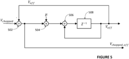
- FIGURE 5 illustrates an exemplary scheme for removing of the offset error, according to some embodiments of the disclosure.
- the offset error V off [ n ] caused by the chopping process can be removed by an offset cancellation circuitry operating on the chopped signal V chopped . Any offset before unchopping can translate into noise after unchopping.
- Equation 6 represents an LMS update equation which can update the estimated offset correction term V off [n] based on a convergence/update coefficient ⁇ and error term ( V chopped [ n ] - V off [ n ]).
- the error term represents the DC/offset error in the chopped signal, which is to be removed.
- the calculation of the error term V chopped [ n ] - V off [ n ] can be performed by summation node 502 which subtracts V chopped [ n ] by V off [ n ] .
- ⁇ ⁇ ( V chopped [ n ] - V off [ n ]) can be performed by multiplier 504, which multiplies V chopped [ n ] - V off [ n ] by convergence coefficient ⁇ .
- V off [ n ] + ⁇ . ( V chopped [ n ] - V off [ n ]) can be performed by summation node 506, which adds ⁇ ⁇ ( V chopped [ n ] - V off [ n ]) and V off [ n ].
- the final result V off [ n ] + ⁇ ⁇ ( V chopped [ n ] - V off [ n ]) is delayed by delay block 508 to form an updated V off [ n + 1].
- V chopped _ off n V chopped n ⁇ V off n
- the offset-corrected chopped output V chopped _ off [ n ] can be obtained by subtracting V off [ n ] from V chopped [ n ] by the summation node 502.
- the code PN is either 0 or 1.
- the presence of gain error means that the ideal gain of the random chopper is no longer exactly 1.
- the gain error can introduces a multiplicative term (1 + PN ⁇ ⁇ c ) to the ideal result of a chopped signal, which was -1 PN ⁇ V in .
- the chopping gain error can be more serious or more detrimental to the signal path than the chopping offset error.
- the gain can be different depending on the state of the random chopper.
- the error term can be considered as V d [ n ] ⁇ ( V chopped [ n ] - f c ( V d [ n ])).
- the pre-chopping dither V d [ n ] is expected to be uncorrelated with the chopped signal with the post-chopping dither removed ( V chopped [ n ] - f c ( V d [ n ])).
- the post-chopping dither can be an estimate of a chopped additive dither (in other words, the additive dither has gone through the chopper).
- Gain error is dependent on chopping state. In other words, the gain can be different depending on the chopping state.
- the error extraction and correction can be done using different approaches.
- different gain error terms are determined separately for each chopping state.
- data associated with a first chopping state is used for updating the gain correction term for the first chopping state
- data associated with a second chopping state is used for updating the gain error term for the second chopping state.
- the data associated with different chopping states are binned by the chopping state when state dependent gain error terms are updated/computed.
- different correction terms can be applied depending on the chopping state.
- the gain of a first chopping state is assumed to be unity or equals to 1
- the gain error of a second chopping state is assumed to be relative to the first chopping state.
- an overall gain estimate can be determined (which addresses both chopping states), and a gain correction term associated with the second chopping state (representing gain relative to the first chopping state) can be used to correct the relative gain error between the two chopping states.
- data associated with the second chopping state (not the data associated with the first chopping state) is used for updating the gain correction term for the second chopping state.
- the chopping state is gating the data being used for updating the gain correction term of for the second chopping state.
- FIGURE 6 illustrates an exemplary scheme for removing the gain error, according to some embodiments of the disclosure.
- the gain error caused by the chopping process can be removed by gain cancellation circuitry operating on the chopped signal V chopped .
- the post-chopping dither f c ( V d [ n ]) is obtained by multiplier 602, which multiplies the pre-chopping dither V d [ n ] and (-(1 + ⁇ c [ n ])) PN [ n ] .
- the post-chopping dither is shown as V d_ch_est in FIGURE 6 .
- Summation node 604 performs ( V chopped [ n ] - f c ( V d [ n ])) by subtracting the chopped signal V chopped [ n ] by post-chopping dither (-(1 + ⁇ c [ n ])) PN [ n ] ⁇ V d [ n ].
- multiplier 606 performs the correlation, i.e., V d [ n ] ⁇ ( V chopped [ n ] - f c ( V d [ n ])), by multiplying ( V chopped [ n ] - f c ( V d [ n ])) and V d [ n ] .
- Multiplier 608 obtains, ⁇ ⁇ V d [ n ] ⁇ ( V chopped [ n ] - f c ( V d [ n ])), by multiplying ⁇ and V d [ n ] ⁇ ( V chopped [ n ] - f c ( V d [ n ])).
- Summation node 610 performs ⁇ c [ n ] - ⁇ ⁇ V d [ n ] ⁇ ( V chopped [ n ] - f c ( V d [ n ])) by adding - ⁇ ⁇ V d [ n ] ⁇ ( V chopped [ n ] - f c ( V d [ n ])) and ⁇ c [ n ] .
- the result of summation node 610 is delayed through delay block 612 to form an updated correction term ⁇ c [ n + 1]. This LMS correlation operation is performed before the unchopping, i.e., on V choppect [ n ] .
- Block 614 takes PN[n] and converged/converging value of ⁇ c as inputs and calculates multiplicative factor (-1/(1 + ⁇ c )) PN [ n ] .
- multiplier 616 multiplies V chopped [ n ] and multiplicative factor (-1/(1 + ⁇ c )) PN [ n ] to obtain the unchopped signal V unchopped_gain [ n ] .
- the multiplicative factors used in obtaining V unchopped_gain [ n ], i.e., (-1/(1 + ⁇ c )) PN [ n ] unchops the signal and accounts for the gain error at the same time.
- FIGURE 7 illustrates yet another exemplary scheme for removing the gain error, corresponding to the LMS equation (13), according to some embodiments of the disclosure.
- the gain error caused by the chopping process can be removed by gain cancellation circuitry operating on the chopped signal V chopped .
- Multiplier 802 performs ⁇ c [ n ] ⁇ V dc [ n ] (shown as dither estimate V d_est in FIGURE 7 ) by multiplying V dc [ n ] and ⁇ c [ n ] .
- Summation node 704 performs ( V chopped [ n ] + ⁇ c [ n ] ⁇ V dc [ n ]) by adding V chopped [ n ] and ⁇ c [ n ] ⁇ V dc [ n ].
- Multiplier 805 performs PN[n] ⁇ ( V chopped [ n ] + ⁇ c [ n ] ⁇ V dc [ n ]) by multiplying PN [ n ] and ( V chopped [ n ] + ⁇ c [ n ] ⁇ V dc [ n ]).
- the final result ⁇ c [ n ] is delayed by delay block 812 to form an updated correction term ⁇ c [ n + 1].
- LMS equation (13) is performed before unchopping, and the converged value for correction term ⁇ c is used for correcting the output. Specifically, the correction term ⁇ c can be used to reduce the gain error.
- block 814 and multiplier 816 obtain the chopped signal with the gain error removed V chopped_gain [ n ].
- Block 814 takes PN [ n ] and converged/converging value of correction term ⁇ c as inputs and calculates multiplicative factor 1 PN ′ n + PN n ⁇ ⁇ c .
- multiplier 816 multiplies V chopped [ n ] and multiplicative factor 1 PN ′ n + PN n ⁇ ⁇ c to obtain the gain error corrected chopped signal V chopped_gain [ n ] .
- Multiplier 908 performs ⁇ ⁇ V dc [ n ] ⁇ PN' [ n ] ⁇ ( V chopped [ n ] - a c 2 [ n ] ⁇ V dc [ n ]) by multiplying convergence coefficient ⁇ and V dc [ n ] ⁇ PN' [ n ] ⁇ ( V chopped [ n ] - ⁇ c2 [ n ] . V dc [ n ]) .
- Summation node 910 performs ⁇ c 2 [ n ] + ⁇ ⁇ V dc [ n ] ⁇ PN' [ n ] ⁇ ( V chopped [ n ] - ⁇ c 2 [ n ] . V dc [ n ]) by adding ⁇ ⁇ V dc [ n ] ⁇ PN '[ n ] ⁇ ( V chopped [ n ] - ⁇ c 2 [ n ] ⁇ V dc [ n ]) and ⁇ c 2 [ n ].
- the final result ⁇ c 2 [ n ] is delayed by delay block 912 to form an updated correction term ⁇ c 2 [ n + 1].
- gain error corrected unchopped signal i.e., V unchopped [ n ] from equation 18 or equation 12
- the additive dither can be removed based on an overall gain correction term.
- FIGURE 9 illustrates an exemplary scheme for removing the additive dither after the errors from chopping are corrected and the signal is unchopped, according to some embodiments of the disclosure.
- Operations of equation (19) are performed on V unchopped , by the dither removal circuitry seen in FIGURE 9 .
- Multiplier 1002 performs G e [ n ] ⁇ V d [ n ] by multiplying V d [ n ] and G e [ n ].
- G e [ n ] ⁇ V d [ n ] which forms a dither estimate based on the dither and the overall gain estimate, is shown as V d_est_g in FIGURE 10 .
- Summation node 1004 performs ( V unchopped [ n ] - G e [ n ] ⁇ V d [ n ]) by subtracting V unchopped [ n ] by G e [ n ] ⁇ V d [ n ].
- inspection points V insp and -V insp are chosen to expose the shape of the non-linear error of interest.
- the inspection points are chosen to expose the odd symmetry associated with a third order distortion, and the inspection points define ranges or open intervals for the counts (cumulative histograms).
- Inspection points can be at the dither amplitude +/-V d , for instance. The counts for when the dither is positive are compared with the counts for when the dither is negative.
- the error term e.g., ⁇ HD 3_1
- the corrected signal V chopped_NL [ n ] is used again by equations (22) and (23) to continue to estimate and update the third order error term in equation (24) and update the value for the correction term ⁇ NL _1 ( n ) using equation (25).
- the partial errors can be combined according to equation 31.
- ⁇ HD 3_2 is a combination of the partial error at the positive inspection point and the partial error at the negative inspection point, which can expose the third order distortion.
- Partial error equations can differ from one implementation to another. Primarily, the partial error equations compare counts/histograms between different values of the dither. However, the values of the dither chosen for the comparison can depend on the implementation. For instance, in various partial error equations, certain values of the dither can be chosen for the comparison (not only +Vd and -Vd). The choice of the values of the dither can vary from one implementation to another. Also, the choice of the values of the dither can depend on the type of non-ideality to be extracted and how the error equations are formulated to extract the non-ideality. Preferably, the values of the dither used in the comparison are chosen to expose or accentuate the shape or pattern associated with the non-ideality. Certain values of the dither signal can result in greater amount of distortion in the output. Choosing those values of the dither signal for the comparison that can cause the greater amount of distortion can make extracting the shape or pattern associated with the non-ideality easier and more effective.
- partial error equations or parameters can vary from one implementation to another.
- partial error equations define ranges based on inspection points, and compare counts/histogram-based on the ranges.
- the definitions of the partial error equations can depend on the type of non-ideality to be extracted.
- various partial error equations or equations defining an error at a given inspection point can use overlapping ranges.
- the type of ranges used in partial error equations can differ from one implementation to another. Alternatively, non-overlapping ranges can be used.
- Instances of Cumsum Vinsp (.) for the positive inspection point V insp can be replaced by Cumsump Vinsp , where Cumsump x ( y ) is the cumulative histogram (i.e., count) of digital codes of digital signal y greater than or equal to x.
- Instances of Cumsum -Vinsp (.) for the negative inspection point -V insp can be replaced by Cumsumn -Vinsp , where Cumsumn x ( y ) is the cumulative histogram (i.e., count) of digital codes of digital signal y less than or equal to x.
- the parameters enhancing even and odd symmetrical errors can also be varied in the same manner to use non-overlapping ranges.
- the opposite equation formulations can also be used in exposing the difference in symmetries for other pairs of error equations and non-linearities.
- Other error formulations are possible so long as they are defined in such a way to expose or accentuate the different shapes associated with various non-idealities. Many examples herein illustrate the flexibility in the approach.
- incremental or sample-by-sample counting can determine whether each sample, i.e., the output with the dither removed, is a hit within the range defined by the inspection point. If the sample, i.e., the output with the dither removed, is a hit, then a value can be assigned to count the sample. Moreover, the comparison between counts can be performed incrementally if a value of +1 is assigned to a hit for one dither value, and a value of -1 is assigned to a hit for another dither value.
- the sign of the pre-chopping dither is the partial error at the inspection point. If the output with the dither removed, e.g., V chopped_NL - V d , is not a hit within the range defined by the inspection point, then the partial error at the inspection point is zero.
- the two partial errors computed in equations (33) and (34) can be combined to form the error ⁇ HD 3_1 and the error ⁇ HD 3_2 . in the same manner as equation (24) and (31).
- the post-chopping dither V dc is used in place of the pre-chopping dither V d .
- the described approaches can be extended to fix other possible kinds of chopping errors. For example, if the chopping is performed in the sampling phase (as opposed to the hold phase as shown in FIGURES 1-3 ), it may cause timing errors. In this case, the same approaches could be used to detect and correct the chopping-dependent timing errors.
- An error formulation can be defined to extract the timing error. Binning/gating can be used by applying PN or PN' appropriately to ensure that different timing error correction terms are computed. In other words, only data associated with a first chopping state is used to compute a first timing error associated with the first chopping state, and only data associated with a second chopping state is used to compute a second timing error associated with the second chopping state. Accordingly, two different correction terms can be obtained and applied to the output depending on the chopping state. It is envisioned by the disclosure that the same approaches can be used to detect and correct other types of chopping-dependent errors not mentioned explicitly herein.
- FIGURE 10 illustrates a converter system 1100 with chopper calibration, according to some embodiments of the disclosure.
- the converter system 1100 can be a data converter, such as an ADC.
- the converter system 1100 includes an input path 1102, quantizer 1104, and digital output path 1106.
- the converter system 1100 receives an analog input signal V in and generates a digital output signal V out representative of the analog input signal V in .
- the input path 1102 receives the analog input signal and includes dither injection 1108 and random chopper 1110.
- the input path 1102 can be implemented based on circuitry illustrated by FIGURES 1-3 and variations thereof.
- the random chopper 1110 can have non-idealities that can affect the performance of the converter system 1100.
- the dither signal being injected (e.g., added) to the input path 1102 in dither injection 1108 and removed in the digital output path 1106 by dither removal 1116 can be used, in certain cases, to extract the non-idealities of the random chopper 1110.
- the additive dither used in dither injection 1108 is not to be confused or construed as the same multiplicative dither used in random chopper 1110. Both dithers are pseudo-random signals but are used differently (and serve different purposes) and would not be the same dither signal.
- the chopped input signal having the dither signal (1112) is quantized by quantizer 1104 to generate a digital version of the chopped input signal having the dither signal (1114).
- the digital output path 1106 receives the digital version of the chopped input signal having the dither signal.
- the digital output path 1106 performs several functions in the digital domain.
- the digital output path 1106 has dither removal 1116, which can remove the dither signal injected by dither injection 1108 and has an unchopper 1118 to unchop the signal in the same way it was chopped by the random chopper 1110.
- the digital output path 1106 has error extraction 1120 to extract the error (e.g., error terms) caused by non-idealities of the random chopper 1110 and correction 1124 to correct the digital output signal by computing one or more correction terms that minimizes the error and generate a final (corrected) V out using the one or more correction terms.
- error e.g., error terms
- correction 1124 can be incorporated with one or more of: dither removal 1116 and unchopper 1118.
- Error extraction 1120 can implement the functionalities for determining error and correction 1124 can determine the correction terms based on the errors.
- Correction 1124 can then apply the correction terms to the digital signal, in cooperation with dither removal 1116 and unchopper 1118, to generate the final corrected unchopped output with the dither signal removed.
- FIGURE 11 is a flow diagram illustrating a method for chopper calibration, according to some embodiments of the disclosure.
- an error of interest is computed based on the chopped digital output and chopping states.
- one or more correction terms are updated to minimize the error.
- the chopped digital output is corrected based on the one or more correction terms.
- the present disclosure encompasses apparatuses which can perform the various methods described herein.
- Such apparatuses can include circuitry illustrated by the FIGURES and described herein.
- Parts of various apparatuses can include electronic circuitry to perform the functions described herein.
- one or more parts of the apparatus can be provided by a processor specially configured for carrying out the functions described herein (e.g., control-related functions, timing-related functions).
- processor can be an on-chip processor with the ADC.
- the processor may include one or more application specific components, or may include programmable logic gates which are configured to carry out the functions describe herein.
- the processor may be configured to carrying out the functions described herein by executing one or more instructions stored on one or more non-transitory computer media.
- references to various features e.g., elements, structures, modules, components, steps, operations, characteristics, etc.
- references to various features e.g., elements, structures, modules, components, steps, operations, characteristics, etc.
- references to various features included in “one embodiment”, “example embodiment”, “an embodiment”, “another embodiment”, “some embodiments”, “various embodiments”, “other embodiments”, “alternative embodiment”, and the like are intended to mean that any such features are included in one or more embodiments of the present disclosure, but may or may not necessarily be combined in the same embodiments.
- the functions described herein illustrate only some of the possible functions that may be executed by, or within, systems/circuits illustrated in the FIGURES. Some of these operations may be deleted or removed where appropriate, or these operations may be modified or changed considerably without departing from the scope of the present disclosure.
Landscapes
- Engineering & Computer Science (AREA)
- Theoretical Computer Science (AREA)
- Analogue/Digital Conversion (AREA)
Claims (12)
- Datenumsetzersystem mit Zerhackerkalibrierung, das umfasst:einen Zerhacker (180), um eine Polarität eines Differenzialanalogsignal zu ändern und ein zerhacktes Differenzialanalogsignal auszugeben;einen Teil zum Einspeisen einer überlagerten Schwingung, um eine zusätzliche überlagerte Schwingung in das Differenzialanalogsignal an einem dem Zerhacker vorgelagerten Schaltungsknoten einzuspeisen, wobei die zusätzliche überlagerte Schwingung einen positiven Wert und einen negativen Wert besitzt;einen Quantisierer (404), um das zerhackte Differenzialanalogsignal in ein zerhacktes Digitalsignal umzusetzen;einen Fehlerextraktionsteil (1120), um einen oder mehrere Fehler, die durch eine oder mehrere Nicht-Idealitäten des Zerhackers verursacht werden, anhand des durch Zustände des Zerhackers und der zusätzlichen überlagerten Schwingung modulierten zerhackten Digitalsignals zu extrahieren, wobei das Bestimmen des einen oder der mehreren Fehler für jeden eines ersten Zustands und eines zweiten Zustands des Zerhackers umfasst:Berechnen eines ersten Teilfehlers an einem positiven Prüfpunkt, eines zweiten Teilfehlers an einem negativen Prüfpunkt und eines Kombinationsfehlers, der einen Unterschied des ersten und des zweiten Teilfehlers umfasst,wobei der erste Teilfehler der Unterschied zwischen einer Zählung, für die das zerhackte Digitalsignal, aus dem die zusätzliche überlagerte Schwingung entfernt wurde, kleiner oder gleich dem positiven Prüfpunkt ist, wenn die überlagerte Schwingung positiv ist, und einer Zählung, für die das zerhackte Digitalsignal, aus dem die zusätzliche überlagerte Schwingung entfernt wurde, kleiner oder gleich dem positiven Prüfpunkt ist, wenn die überlagerte Schwingung negativ ist, ist,wobei der zweite Teilfehler der Unterschied zwischen einer Zählung, für die das zerhackte Digitalsignal, von dem die zusätzliche überlagerte Schwingung entfernt wurde, kleiner oder gleich dem negativen Prüfpunkt ist, wenn die überlagerte Schwingung positiv ist, und einer Zählung, für die das zerhackte Digitalsignal, von dem die zusätzliche überlagerte Schwingung entfernt wurde, kleiner oder gleich dem negativen Prüfpunkt ist, wenn die überlagerte Schwingung negativ ist, ist undwobei der positive Prüfpunkt und der negative Prüfpunkt jeweils ein positiver und ein negativer Wert der zusätzlichen überlagerten Schwingung sind; undeinen Korrekturteil (1124), um einen ersten Korrekturausdruck, der dem ersten Zustand des Zerhackers entspricht, anhand eines ersten Kombinationsfehlers, der aus dem zerhackten Digitalsignal, das durch den ersten Zustand des Zerhackers moduliert wurde, extrahiert wurde, zu aktualisieren und (2) einen zweiten Korrekturausdruck, der dem zweiten Zustand des Zerhackers entspricht, anhand eines zweiten Kombinationsfehlers, der aus dem zerhackten Digitalsignal, das durch den zweiten Zustand des Zerhackers moduliert wurde, extrahiert wurde, zu aktualisieren, wobei der erste und der zweite Korrekturausdruck durch Verwenden der extrahierten Fehlerausdrücke in einer Gleichung kleinster mittlerer Quadrate, LMS-Gleichung, aktualisiert werden, um den einen oder die mehreren Fehler zu verringern und den ersten und den zweiten Korrekturausdruck auf das zerhackte Digitalsignal anzuwenden.
- Datenumsetzersystem nach Anspruch 1, wobei der Fehlerextraktionsteil (1120) den einen oder die mehreren Fehler durch Subtrahieren des zerhackten Digitalsignals durch einen Versatzkorrekturausdruck, der durch den Korrekturteil aktualisiert wird, extrahiert.
- Datenumsetzersystem nach Anspruch 1 oder 2, das ferner umfasst:
einen Summierer (410), um eine Stärke der zusätzlichen überlagerten Schwingung, die durch den dem Quantisierer (404) nachgelagerten Teil zum Einspeisen einer überlagerten Schwingung eingespeist wird, zu subtrahieren. - Datenumsetzersystem nach einem vorhergehenden Anspruch, wobei die Fehler einen oder mehrere der folgenden Fehler umfassen: Verstärkungsfehler des Zerhackers, nichtlineare Fehler des Zerhackers und Zeitfehler des Zerhackers.
- Datenumsetzersystem nach einem vorhergehenden Anspruch, wobei der Korrekturteil (1124) einen ersten und einen zweiten multiplikativen Faktor anhand des ersten und des zweiten Korrekturausdrucks bestimmen soll und den ersten und den zweiten multiplikativen Faktor auf das zerhackte Digitalsignal anwendet, um den einen oder die mehreren Fehler zu verringern und vorzugsweise die Zerhackung des zerhackten Signals aufzuheben.
- Datenumsetzersystem nach einem vorhergehenden Anspruch, wobei der Fehlerextraktionsteil (1120) ausführen soll:
Modulieren des Vergleichens der kumulativen Histogramme durch die Zustände des Zerhackers (108). - Datenumsetzersystem nach einem vorhergehenden Anspruch, wobei der Korrekturteil (1124) den ersten und den zweiten Korrekturausdruck anhand eines Fehlerausdrucks, der durch das zerhackte Digitalsignal und einen Korrekturausdruck definiert wird, aktualisieren soll.
- Verfahren zum digitalen Korrigieren einer Analogschaltung mit einem Zerhacker (108), das umfasst:Einspeisen einer zusätzlichen überlagerten Schwingung in die Analogschaltung in einen dem Zerhacker (108) vorgelagerten Schaltungsknoten, wobei die zusätzliche überlagerte Schwingung einen verschiedenen positiven Wert und negativen Wert umfasst;Bestimmen (202) eines oder mehrerer Fehlerausdrücke, die durch eine oder mehrere Nicht-Idealitäten des Zerhackers verursacht werden, anhand eines durch Zustände des Zerhackers und der zusätzlichen überlagerten Schwingung modulierten zerhackten Digitalsignals, wobei das Bestimmen des einen oder der mehreren Fehler für jeden eines ersten Zustands und eines zweiten Zustands des Zerhackers umfasst:Berechnen eines ersten Teilfehlers an einem positiven Prüfpunkt, eines zweiten Teilfehlers an einem negativen Prüfpunkt und eines Kombinationsfehlers, der einen Unterschied des ersten und des zweiten Teilfehlers umfasst,wobei der erste Teilfehler der Unterschied zwischen einer Zählung, für die das zerhackte Digitalsignal, von dem die zusätzliche überlagerte Schwingung entfernt wurde, kleiner oder gleich dem positiven Prüfpunkt ist, wenn die überlagerte Schwingung positiv ist, und einer Zählung, für die das zerhackte Digitalsignal, von dem die zusätzliche überlagerte Schwingung entfernt wurde, kleiner oder gleich dem positiven Prüfpunkt ist, wenn die überlagerte Schwingung negativ ist, ist,wobei der zweite Teilfehler der Unterschied zwischen einer Zählung, für die das zerhackte Digitalsignal, von dem die zusätzliche überlagerte Schwingung entfernt wurde, kleiner oder gleich dem negativen Prüfpunkt ist, wenn die überlagerte Schwingung positiv ist, und einer Zählung, für die das zerhackte Digitalsignal, von dem die zusätzliche überlagerte Schwingung entfernt wurde, kleiner oder gleich dem negativen Prüfpunkt ist, wenn die überlagerte Schwingung negativ ist, ist undwobei der positive Prüfpunkt und der negative Prüfpunkt jeweils ein positiver und ein negativer Wert der zusätzlichen überlagerten Schwingung sind;Aktualisieren (1204) (1) eines ersten Korrekturausdrucks, der dem ersten Zustand des Zerhacker entspricht, anhand eines ersten Kombinationsfehlers, der aus dem zerhackten Digitalsignal, das durch den ersten Zustand des Zerhackers moduliert wurde, extrahiert wurde, und (2) eines zweiten Korrekturausdrucks, der dem zweiten Zustand des Zerhackers entspricht, anhand eines zweiten Kombinationsfehlers, der aus dem zerhackten Digitalsignal, das durch den zweiten Zustand des Zerhackers moduliert wurde, extrahiert wurde, wobei der erste und der zweite Korrekturausdruck durch Verwenden der extrahierten Fehlerausdrücke in einer Gleichung kleinster mittlerer Quadrate, LMS-Gleichung, aktualisiert werden, um den einen oder die mehreren Fehlerausdrücke zu verringern; undKorrigieren (1206) und Aufheben der Zerhackung der zerhackten digitalen Ausgabe anhand des ersten und des zweiten Korrekturausdrucks.
- Verfahren nach Anspruch 8, das ferner umfasst:
Subtrahieren eines Werts der zusätzlichen überlagerten Schwingung in einem digitalen Ausgangsweg (406). - Verfahren nach Anspruch 9, wobei die Fehlerausdrücke einen oder mehrere der folgenden Fehler umfassen: Verstärkungsfehler des Zerhackers, nichtlineare Fehler des Zerhackers und Zeitfehler des Zerhackers.
- Verfahren nach einem der Ansprüche 8-10, wobei das Korrigieren und Aufheben der Zerhackung der zerhackten digitalen Ausgabe anhand des ersten und des zweiten Korrekturausdrucks umfasst:Bestimmen eines ersten multiplikativen Faktors anhand des ersten Korrekturausdrucks, der dem ersten Zustand des Zerhackers entspricht; undMultiplizieren der zerhackten digitalen Ausgabe mit dem ersten multiplikativen Faktor als Reaktion darauf, dass der Zerhacker in dem ersten der Zustände des Zerhackers ist.
- Verfahren nach einem der Ansprüche 9-11, das ferner umfasst:
Entfernen der zusätzlichen überlagerten Schwingung durch Subtrahieren der zusätzlichen überlagerten Schwingung multipliziert mit einem Verstärkungskorrekturausdruck von einem digitalen Signal, dessen Zerhackung aufgehoben wurde.
Applications Claiming Priority (2)
| Application Number | Priority Date | Filing Date | Title |
|---|---|---|---|
| US201862637605P | 2018-03-02 | 2018-03-02 | |
| US16/265,317 US10715162B2 (en) | 2018-03-02 | 2019-02-01 | Background calibration of random chopping non-idealities in data converters |
Publications (2)
| Publication Number | Publication Date |
|---|---|
| EP3534540A1 EP3534540A1 (de) | 2019-09-04 |
| EP3534540B1 true EP3534540B1 (de) | 2024-07-17 |
Family
ID=65657377
Family Applications (1)
| Application Number | Title | Priority Date | Filing Date |
|---|---|---|---|
| EP19160286.1A Active EP3534540B1 (de) | 2018-03-02 | 2019-03-01 | Hintergrundkalibrierung von zufälligen schnittfehlern in datenwandlern |
Country Status (3)
| Country | Link |
|---|---|
| US (2) | US10715162B2 (de) |
| EP (1) | EP3534540B1 (de) |
| CN (1) | CN110224698B (de) |
Families Citing this family (1)
| Publication number | Priority date | Publication date | Assignee | Title |
|---|---|---|---|---|
| US11593573B2 (en) * | 2021-05-31 | 2023-02-28 | Ceremorphic, Inc. | Chopper stabilized analog multiplier unit element with binary weighted charge transfer capacitors |
Citations (1)
| Publication number | Priority date | Publication date | Assignee | Title |
|---|---|---|---|---|
| US9859907B1 (en) * | 2016-10-28 | 2018-01-02 | Analog Devices, Inc. | Systems and methods for removing errors in analog to digital converter signal chain |
Family Cites Families (6)
| Publication number | Priority date | Publication date | Assignee | Title |
|---|---|---|---|---|
| DE102006046966A1 (de) * | 2006-05-26 | 2007-11-29 | Rohde & Schwarz Gmbh & Co. Kg | Messvorrichtung und Messverfahren zum Messen der Leistung eines Hochfrequenzsignals |
| US9356568B2 (en) | 2007-06-05 | 2016-05-31 | Analog Devices, Inc. | Apparatus and methods for chopper amplifiers |
| US8525710B1 (en) | 2010-03-31 | 2013-09-03 | Cirrus Logic, Inc. | Audio amplifier offset reduction using digital input/output comparisons |
| JP2014165658A (ja) * | 2013-02-25 | 2014-09-08 | Toshiba Corp | Ad変換器 |
| US9143147B1 (en) | 2014-07-03 | 2015-09-22 | Keysight Technologies, Inc. | Calibration of inter-slice gain and offset errors in time-interleaved analog-to- digital converter |
| US9654133B2 (en) * | 2014-12-17 | 2017-05-16 | Analog Devices, Inc. | Microprocessor-assisted calibration for analog-to-digital converter |
-
2019
- 2019-02-01 US US16/265,317 patent/US10715162B2/en active Active
- 2019-03-01 EP EP19160286.1A patent/EP3534540B1/de active Active
- 2019-03-01 CN CN201910154495.6A patent/CN110224698B/zh active Active
-
2020
- 2020-07-13 US US16/927,019 patent/US11057043B2/en active Active
Patent Citations (1)
| Publication number | Priority date | Publication date | Assignee | Title |
|---|---|---|---|---|
| US9859907B1 (en) * | 2016-10-28 | 2018-01-02 | Analog Devices, Inc. | Systems and methods for removing errors in analog to digital converter signal chain |
Non-Patent Citations (5)
| Title |
|---|
| BALÁZS RENCZES ET AL: "Compensation of Analog-to-Digital Converter Nonlinearities using Dither", PERIODICA POLYTECHNICA ELECTRICAL ENGINEERING, vol. 57, no. 3, 1 January 2013 (2013-01-01), pages 77, XP055325351, ISSN: 0031-532X, DOI: 10.3311/PPee.2145 * |
| BROOKS L ET AL: "Background Calibration of Pipelined ADCs Via Decision Boundary Gap Estimation", IEEE TRANSACTIONS ON CIRCUITS AND SYSTEMS I: REGULAR PAPERS, IEEE, US, vol. 55, no. 10, 1 November 2008 (2008-11-01), pages 2969 - 2979, XP011333304, ISSN: 1549-8328, DOI: 10.1109/TCSI.2008.925373 * |
| HUAYU JIA ET AL: "Improved Digital Calibration Technology in a 12-b, 40-MS/s Pipelined ADC", 2007 7TH INTERNATIONAL CONFERENCE ON ASIC, 22 October 2007 (2007-10-22), Guilin, China, pages 261 - 264, XP093093176, ISSN: 2162-7541, ISBN: 978-1-4244-1131-3, Retrieved from the Internet <URL:https://ieeexplore.ieee.org/stampPDF/getPDF.jsp?tp=&arnumber=4415617&ref=aHR0cHM6Ly9pZWVleHBsb3JlLmllZWUub3JnL2RvY3VtZW50LzQ0MTU2MTc=> DOI: 10.1109/ICASIC.2007.4415617 * |
| MURMANN B ET AL: "A 12-BIT 75-MS/S PIPELINED ADC USING OPEN-LOOP RESIDUE AMPLIFICATION", IEEE JOURNAL OF SOLID-STATE CIRCUITS, IEEE, USA, vol. 38, no. 12, 1 December 2003 (2003-12-01), pages 2040 - 2050, XP001221453, ISSN: 0018-9200, DOI: 10.1109/JSSC.2003.819167 * |
| VERBRUGGEN BOB ET AL: "A 2.1 mW 11b 410 MS/s dynamic pipelined SAR ADC with background calibration in 28nm digital CMOS", 2013 SYMPOSIUM ON VLSI CIRCUITS, IEEE, 12 June 2013 (2013-06-12), XP032474916, ISBN: 978-1-4673-5531-5, [retrieved on 20130813] * |
Also Published As
| Publication number | Publication date |
|---|---|
| US10715162B2 (en) | 2020-07-14 |
| CN110224698B (zh) | 2023-10-13 |
| US11057043B2 (en) | 2021-07-06 |
| US20200350921A1 (en) | 2020-11-05 |
| US20190273505A1 (en) | 2019-09-05 |
| CN110224698A (zh) | 2019-09-10 |
| EP3534540A1 (de) | 2019-09-04 |
Similar Documents
| Publication | Publication Date | Title |
|---|---|---|
| US10763878B2 (en) | Calibrating time-interleaved switched-capacitor track-and-hold circuits and amplifiers | |
| US10547319B2 (en) | Background calibration of reference, DAC, and quantization non-linearity in ADCS | |
| US9143147B1 (en) | Calibration of inter-slice gain and offset errors in time-interleaved analog-to- digital converter | |
| EP3742615B1 (de) | Vco-basierte continuous-time-pipeline-adc | |
| US10340934B1 (en) | Signal path linearization | |
| US10432210B1 (en) | Oversampled continuous-time pipeline ADC with digital signal reconstruction | |
| US11159169B2 (en) | Background calibration of non-linearity of samplers and amplifiers in ADCs | |
| US9945901B1 (en) | Measuring and correcting non-idealities of a system | |
| JP4754941B2 (ja) | 線形補正器 | |
| US11652491B2 (en) | High-pass shaped dither in continuous-time residue generation systems for analog-to-digital converters | |
| CN108494403A (zh) | 一种双通道tiadc采样保持电路失配自适应校准方法 | |
| Wang et al. | Adaptive background estimation for static nonlinearity mismatches in two-channel TIADCs | |
| EP3534540B1 (de) | Hintergrundkalibrierung von zufälligen schnittfehlern in datenwandlern | |
| US20110122005A1 (en) | method to linearize the output from an adc | |
| EP2779461B1 (de) | Verfahren und Vorrichtung zur Verbesserung der Konvergenzzeit in korrelationsbasierten Algorithmen | |
| Ta et al. | Fully digital background calibration technique for channel mismatches in TIADCs | |
| Le Duc et al. | Estimation techniques for timing mismatch in time-interleaved analog-to-digital converters: Limitations and solutions | |
| EP3182598B1 (de) | Signalübertragungsfunktionsentzerrung in mehrstufigen delta-sigma-analog-digital-umsetzern | |
| US20240364356A1 (en) | Continuous-time adc calibration techniques | |
| Wei et al. | Calibration of static nonlinearity mismatch errors in TIADC based on periodic time-varying adaptive method | |
| Leene et al. | A compact recording array for neural interfaces | |
| Dubois et al. | ADC low-complexity modelling identification and mitigation of baseband intermodulation distortion with instantaneous frequency dependence | |
| Liu et al. | A low-complexity timing mismatch calibration method for four-channel time-interleaved ADCs based on cross correlation | |
| Jiang et al. | Dynamic pre-compensation of memory nonlinear distortion for high-speed signal generator based on Volterra inverse | |
| Wolfer et al. | Performance and stability characterization of a 3rd order continuous-time delta-sigma modulator with active time-constant tuning |
Legal Events
| Date | Code | Title | Description |
|---|---|---|---|
| PUAI | Public reference made under article 153(3) epc to a published international application that has entered the european phase |
Free format text: ORIGINAL CODE: 0009012 |
|
| STAA | Information on the status of an ep patent application or granted ep patent |
Free format text: STATUS: THE APPLICATION HAS BEEN PUBLISHED |
|
| AK | Designated contracting states |
Kind code of ref document: A1 Designated state(s): AL AT BE BG CH CY CZ DE DK EE ES FI FR GB GR HR HU IE IS IT LI LT LU LV MC MK MT NL NO PL PT RO RS SE SI SK SM TR |
|
| AX | Request for extension of the european patent |
Extension state: BA ME |
|
| STAA | Information on the status of an ep patent application or granted ep patent |
Free format text: STATUS: REQUEST FOR EXAMINATION WAS MADE |
|
| 17P | Request for examination filed |
Effective date: 20200204 |
|
| RBV | Designated contracting states (corrected) |
Designated state(s): AL AT BE BG CH CY CZ DE DK EE ES FI FR GB GR HR HU IE IS IT LI LT LU LV MC MK MT NL NO PL PT RO RS SE SI SK SM TR |
|
| RAP3 | Party data changed (applicant data changed or rights of an application transferred) |
Owner name: ANALOG DEVICES, INC. |
|
| STAA | Information on the status of an ep patent application or granted ep patent |
Free format text: STATUS: EXAMINATION IS IN PROGRESS |
|
| 17Q | First examination report despatched |
Effective date: 20211015 |
|
| GRAP | Despatch of communication of intention to grant a patent |
Free format text: ORIGINAL CODE: EPIDOSNIGR1 |
|
| STAA | Information on the status of an ep patent application or granted ep patent |
Free format text: STATUS: GRANT OF PATENT IS INTENDED |
|
| RIC1 | Information provided on ipc code assigned before grant |
Ipc: H03M 1/12 20060101ALN20240405BHEP Ipc: H03M 1/10 20060101AFI20240405BHEP |
|
| INTG | Intention to grant announced |
Effective date: 20240426 |
|
| GRAS | Grant fee paid |
Free format text: ORIGINAL CODE: EPIDOSNIGR3 |
|
| GRAA | (expected) grant |
Free format text: ORIGINAL CODE: 0009210 |
|
| STAA | Information on the status of an ep patent application or granted ep patent |
Free format text: STATUS: THE PATENT HAS BEEN GRANTED |
|
| AK | Designated contracting states |
Kind code of ref document: B1 Designated state(s): AL AT BE BG CH CY CZ DE DK EE ES FI FR GB GR HR HU IE IS IT LI LT LU LV MC MK MT NL NO PL PT RO RS SE SI SK SM TR |
|
| REG | Reference to a national code |
Ref country code: CH Ref legal event code: EP |
|
| REG | Reference to a national code |
Ref country code: DE Ref legal event code: R096 Ref document number: 602019055250 Country of ref document: DE |
|
| REG | Reference to a national code |
Ref country code: IE Ref legal event code: FG4D |
|
| REG | Reference to a national code |
Ref country code: LT Ref legal event code: MG9D |
|
| REG | Reference to a national code |
Ref country code: NL Ref legal event code: MP Effective date: 20240717 |
|
| PG25 | Lapsed in a contracting state [announced via postgrant information from national office to epo] |
Ref country code: PT Free format text: LAPSE BECAUSE OF FAILURE TO SUBMIT A TRANSLATION OF THE DESCRIPTION OR TO PAY THE FEE WITHIN THE PRESCRIBED TIME-LIMIT Effective date: 20241118 |
|
| REG | Reference to a national code |
Ref country code: AT Ref legal event code: MK05 Ref document number: 1705090 Country of ref document: AT Kind code of ref document: T Effective date: 20240717 |
|
| PG25 | Lapsed in a contracting state [announced via postgrant information from national office to epo] |
Ref country code: NL Free format text: LAPSE BECAUSE OF FAILURE TO SUBMIT A TRANSLATION OF THE DESCRIPTION OR TO PAY THE FEE WITHIN THE PRESCRIBED TIME-LIMIT Effective date: 20240717 |
|
| PG25 | Lapsed in a contracting state [announced via postgrant information from national office to epo] |
Ref country code: PT Free format text: LAPSE BECAUSE OF FAILURE TO SUBMIT A TRANSLATION OF THE DESCRIPTION OR TO PAY THE FEE WITHIN THE PRESCRIBED TIME-LIMIT Effective date: 20241118 Ref country code: NL Free format text: LAPSE BECAUSE OF FAILURE TO SUBMIT A TRANSLATION OF THE DESCRIPTION OR TO PAY THE FEE WITHIN THE PRESCRIBED TIME-LIMIT Effective date: 20240717 |
|
| PG25 | Lapsed in a contracting state [announced via postgrant information from national office to epo] |
Ref country code: NO Free format text: LAPSE BECAUSE OF FAILURE TO SUBMIT A TRANSLATION OF THE DESCRIPTION OR TO PAY THE FEE WITHIN THE PRESCRIBED TIME-LIMIT Effective date: 20241017 |
|
| PG25 | Lapsed in a contracting state [announced via postgrant information from national office to epo] |
Ref country code: FI Free format text: LAPSE BECAUSE OF FAILURE TO SUBMIT A TRANSLATION OF THE DESCRIPTION OR TO PAY THE FEE WITHIN THE PRESCRIBED TIME-LIMIT Effective date: 20240717 Ref country code: GR Free format text: LAPSE BECAUSE OF FAILURE TO SUBMIT A TRANSLATION OF THE DESCRIPTION OR TO PAY THE FEE WITHIN THE PRESCRIBED TIME-LIMIT Effective date: 20241018 Ref country code: PL Free format text: LAPSE BECAUSE OF FAILURE TO SUBMIT A TRANSLATION OF THE DESCRIPTION OR TO PAY THE FEE WITHIN THE PRESCRIBED TIME-LIMIT Effective date: 20240717 |
|
| PG25 | Lapsed in a contracting state [announced via postgrant information from national office to epo] |
Ref country code: BG Free format text: LAPSE BECAUSE OF FAILURE TO SUBMIT A TRANSLATION OF THE DESCRIPTION OR TO PAY THE FEE WITHIN THE PRESCRIBED TIME-LIMIT Effective date: 20240717 |
|
| PG25 | Lapsed in a contracting state [announced via postgrant information from national office to epo] |
Ref country code: LV Free format text: LAPSE BECAUSE OF FAILURE TO SUBMIT A TRANSLATION OF THE DESCRIPTION OR TO PAY THE FEE WITHIN THE PRESCRIBED TIME-LIMIT Effective date: 20240717 |
|
| PG25 | Lapsed in a contracting state [announced via postgrant information from national office to epo] |
Ref country code: IS Free format text: LAPSE BECAUSE OF FAILURE TO SUBMIT A TRANSLATION OF THE DESCRIPTION OR TO PAY THE FEE WITHIN THE PRESCRIBED TIME-LIMIT Effective date: 20241117 Ref country code: AT Free format text: LAPSE BECAUSE OF FAILURE TO SUBMIT A TRANSLATION OF THE DESCRIPTION OR TO PAY THE FEE WITHIN THE PRESCRIBED TIME-LIMIT Effective date: 20240717 |
|
| PG25 | Lapsed in a contracting state [announced via postgrant information from national office to epo] |
Ref country code: HR Free format text: LAPSE BECAUSE OF FAILURE TO SUBMIT A TRANSLATION OF THE DESCRIPTION OR TO PAY THE FEE WITHIN THE PRESCRIBED TIME-LIMIT Effective date: 20240717 |
|
| PG25 | Lapsed in a contracting state [announced via postgrant information from national office to epo] |
Ref country code: RS Free format text: LAPSE BECAUSE OF FAILURE TO SUBMIT A TRANSLATION OF THE DESCRIPTION OR TO PAY THE FEE WITHIN THE PRESCRIBED TIME-LIMIT Effective date: 20241017 Ref country code: ES Free format text: LAPSE BECAUSE OF FAILURE TO SUBMIT A TRANSLATION OF THE DESCRIPTION OR TO PAY THE FEE WITHIN THE PRESCRIBED TIME-LIMIT Effective date: 20240717 |
|
| PG25 | Lapsed in a contracting state [announced via postgrant information from national office to epo] |
Ref country code: RS Free format text: LAPSE BECAUSE OF FAILURE TO SUBMIT A TRANSLATION OF THE DESCRIPTION OR TO PAY THE FEE WITHIN THE PRESCRIBED TIME-LIMIT Effective date: 20241017 Ref country code: PL Free format text: LAPSE BECAUSE OF FAILURE TO SUBMIT A TRANSLATION OF THE DESCRIPTION OR TO PAY THE FEE WITHIN THE PRESCRIBED TIME-LIMIT Effective date: 20240717 Ref country code: NO Free format text: LAPSE BECAUSE OF FAILURE TO SUBMIT A TRANSLATION OF THE DESCRIPTION OR TO PAY THE FEE WITHIN THE PRESCRIBED TIME-LIMIT Effective date: 20241017 Ref country code: LV Free format text: LAPSE BECAUSE OF FAILURE TO SUBMIT A TRANSLATION OF THE DESCRIPTION OR TO PAY THE FEE WITHIN THE PRESCRIBED TIME-LIMIT Effective date: 20240717 Ref country code: IS Free format text: LAPSE BECAUSE OF FAILURE TO SUBMIT A TRANSLATION OF THE DESCRIPTION OR TO PAY THE FEE WITHIN THE PRESCRIBED TIME-LIMIT Effective date: 20241117 Ref country code: HR Free format text: LAPSE BECAUSE OF FAILURE TO SUBMIT A TRANSLATION OF THE DESCRIPTION OR TO PAY THE FEE WITHIN THE PRESCRIBED TIME-LIMIT Effective date: 20240717 Ref country code: GR Free format text: LAPSE BECAUSE OF FAILURE TO SUBMIT A TRANSLATION OF THE DESCRIPTION OR TO PAY THE FEE WITHIN THE PRESCRIBED TIME-LIMIT Effective date: 20241018 Ref country code: FI Free format text: LAPSE BECAUSE OF FAILURE TO SUBMIT A TRANSLATION OF THE DESCRIPTION OR TO PAY THE FEE WITHIN THE PRESCRIBED TIME-LIMIT Effective date: 20240717 Ref country code: ES Free format text: LAPSE BECAUSE OF FAILURE TO SUBMIT A TRANSLATION OF THE DESCRIPTION OR TO PAY THE FEE WITHIN THE PRESCRIBED TIME-LIMIT Effective date: 20240717 Ref country code: BG Free format text: LAPSE BECAUSE OF FAILURE TO SUBMIT A TRANSLATION OF THE DESCRIPTION OR TO PAY THE FEE WITHIN THE PRESCRIBED TIME-LIMIT Effective date: 20240717 Ref country code: AT Free format text: LAPSE BECAUSE OF FAILURE TO SUBMIT A TRANSLATION OF THE DESCRIPTION OR TO PAY THE FEE WITHIN THE PRESCRIBED TIME-LIMIT Effective date: 20240717 |
|
| PGFP | Annual fee paid to national office [announced via postgrant information from national office to epo] |
Ref country code: DE Payment date: 20250218 Year of fee payment: 7 |
|
| PG25 | Lapsed in a contracting state [announced via postgrant information from national office to epo] |
Ref country code: RO Free format text: LAPSE BECAUSE OF FAILURE TO SUBMIT A TRANSLATION OF THE DESCRIPTION OR TO PAY THE FEE WITHIN THE PRESCRIBED TIME-LIMIT Effective date: 20240717 Ref country code: DK Free format text: LAPSE BECAUSE OF FAILURE TO SUBMIT A TRANSLATION OF THE DESCRIPTION OR TO PAY THE FEE WITHIN THE PRESCRIBED TIME-LIMIT Effective date: 20240717 Ref country code: SM Free format text: LAPSE BECAUSE OF FAILURE TO SUBMIT A TRANSLATION OF THE DESCRIPTION OR TO PAY THE FEE WITHIN THE PRESCRIBED TIME-LIMIT Effective date: 20240717 |
|
| REG | Reference to a national code |
Ref country code: DE Ref legal event code: R097 Ref document number: 602019055250 Country of ref document: DE |
|
| PG25 | Lapsed in a contracting state [announced via postgrant information from national office to epo] |
Ref country code: EE Free format text: LAPSE BECAUSE OF FAILURE TO SUBMIT A TRANSLATION OF THE DESCRIPTION OR TO PAY THE FEE WITHIN THE PRESCRIBED TIME-LIMIT Effective date: 20240717 |
|
| PG25 | Lapsed in a contracting state [announced via postgrant information from national office to epo] |
Ref country code: CZ Free format text: LAPSE BECAUSE OF FAILURE TO SUBMIT A TRANSLATION OF THE DESCRIPTION OR TO PAY THE FEE WITHIN THE PRESCRIBED TIME-LIMIT Effective date: 20240717 |
|
| PGFP | Annual fee paid to national office [announced via postgrant information from national office to epo] |
Ref country code: FR Payment date: 20250218 Year of fee payment: 7 |
|
| PG25 | Lapsed in a contracting state [announced via postgrant information from national office to epo] |
Ref country code: SK Free format text: LAPSE BECAUSE OF FAILURE TO SUBMIT A TRANSLATION OF THE DESCRIPTION OR TO PAY THE FEE WITHIN THE PRESCRIBED TIME-LIMIT Effective date: 20240717 |
|
| PGFP | Annual fee paid to national office [announced via postgrant information from national office to epo] |
Ref country code: GB Payment date: 20250220 Year of fee payment: 7 |
|
| PLBE | No opposition filed within time limit |
Free format text: ORIGINAL CODE: 0009261 |
|
| STAA | Information on the status of an ep patent application or granted ep patent |
Free format text: STATUS: NO OPPOSITION FILED WITHIN TIME LIMIT |
|
| 26N | No opposition filed |
Effective date: 20250422 |
|
| PG25 | Lapsed in a contracting state [announced via postgrant information from national office to epo] |
Ref country code: SE Free format text: LAPSE BECAUSE OF FAILURE TO SUBMIT A TRANSLATION OF THE DESCRIPTION OR TO PAY THE FEE WITHIN THE PRESCRIBED TIME-LIMIT Effective date: 20240717 |
|
| PG25 | Lapsed in a contracting state [announced via postgrant information from national office to epo] |
Ref country code: MC Free format text: LAPSE BECAUSE OF FAILURE TO SUBMIT A TRANSLATION OF THE DESCRIPTION OR TO PAY THE FEE WITHIN THE PRESCRIBED TIME-LIMIT Effective date: 20240717 |
|
| REG | Reference to a national code |
Ref country code: CH Ref legal event code: H13 Free format text: ST27 STATUS EVENT CODE: U-0-0-H10-H13 (AS PROVIDED BY THE NATIONAL OFFICE) Effective date: 20251023 |
|
| PG25 | Lapsed in a contracting state [announced via postgrant information from national office to epo] |
Ref country code: LU Free format text: LAPSE BECAUSE OF NON-PAYMENT OF DUE FEES Effective date: 20250301 |
|
| REG | Reference to a national code |
Ref country code: BE Ref legal event code: MM Effective date: 20250331 |
|
| PG25 | Lapsed in a contracting state [announced via postgrant information from national office to epo] |
Ref country code: BE Free format text: LAPSE BECAUSE OF NON-PAYMENT OF DUE FEES Effective date: 20250331 |
|
| PG25 | Lapsed in a contracting state [announced via postgrant information from national office to epo] |
Ref country code: CH Free format text: LAPSE BECAUSE OF NON-PAYMENT OF DUE FEES Effective date: 20250331 |
|
| PG25 | Lapsed in a contracting state [announced via postgrant information from national office to epo] |
Ref country code: IE Free format text: LAPSE BECAUSE OF NON-PAYMENT OF DUE FEES Effective date: 20250301 |
|
| PG25 | Lapsed in a contracting state [announced via postgrant information from national office to epo] |
Ref country code: IT Free format text: LAPSE BECAUSE OF FAILURE TO SUBMIT A TRANSLATION OF THE DESCRIPTION OR TO PAY THE FEE WITHIN THE PRESCRIBED TIME-LIMIT Effective date: 20240717 |