EP2779406A2 - Convertisseur de puissance et climatiseur comportant celui-ci - Google Patents
Convertisseur de puissance et climatiseur comportant celui-ci Download PDFInfo
- Publication number
- EP2779406A2 EP2779406A2 EP14159054.7A EP14159054A EP2779406A2 EP 2779406 A2 EP2779406 A2 EP 2779406A2 EP 14159054 A EP14159054 A EP 14159054A EP 2779406 A2 EP2779406 A2 EP 2779406A2
- Authority
- EP
- European Patent Office
- Prior art keywords
- converter
- power
- switching element
- interleave
- capacitor
- Prior art date
- Legal status (The legal status is an assumption and is not a legal conclusion. Google has not performed a legal analysis and makes no representation as to the accuracy of the status listed.)
- Granted
Links
- 239000003990 capacitor Substances 0.000 claims abstract description 59
- 230000005669 field effect Effects 0.000 claims description 2
- 229910044991 metal oxide Inorganic materials 0.000 claims description 2
- 150000004706 metal oxides Chemical class 0.000 claims description 2
- 239000004065 semiconductor Substances 0.000 claims description 2
- 238000010586 diagram Methods 0.000 description 22
- 239000003507 refrigerant Substances 0.000 description 14
- 230000009466 transformation Effects 0.000 description 10
- 101100354370 Mus musculus Ptprj gene Proteins 0.000 description 9
- 101001024120 Homo sapiens Nipped-B-like protein Proteins 0.000 description 7
- 102100035377 Nipped-B-like protein Human genes 0.000 description 7
- 238000001816 cooling Methods 0.000 description 7
- 238000010438 heat treatment Methods 0.000 description 5
- 230000017525 heat dissipation Effects 0.000 description 4
- 230000004044 response Effects 0.000 description 4
- 230000001360 synchronised effect Effects 0.000 description 3
- 238000006243 chemical reaction Methods 0.000 description 2
- 238000007599 discharging Methods 0.000 description 2
- 230000006870 function Effects 0.000 description 2
- 238000009499 grossing Methods 0.000 description 2
- 238000000034 method Methods 0.000 description 2
- 238000012986 modification Methods 0.000 description 2
- 230000004048 modification Effects 0.000 description 2
- 230000005540 biological transmission Effects 0.000 description 1
- 230000006835 compression Effects 0.000 description 1
- 238000007906 compression Methods 0.000 description 1
- 238000001514 detection method Methods 0.000 description 1
- 238000001914 filtration Methods 0.000 description 1
- 230000001939 inductive effect Effects 0.000 description 1
- XLYOFNOQVPJJNP-UHFFFAOYSA-N water Substances O XLYOFNOQVPJJNP-UHFFFAOYSA-N 0.000 description 1
Images


Classifications
-
- H—ELECTRICITY
- H02—GENERATION; CONVERSION OR DISTRIBUTION OF ELECTRIC POWER
- H02P—CONTROL OR REGULATION OF ELECTRIC MOTORS, ELECTRIC GENERATORS OR DYNAMO-ELECTRIC CONVERTERS; CONTROLLING TRANSFORMERS, REACTORS OR CHOKE COILS
- H02P27/00—Arrangements or methods for the control of AC motors characterised by the kind of supply voltage
- H02P27/04—Arrangements or methods for the control of AC motors characterised by the kind of supply voltage using variable-frequency supply voltage, e.g. inverter or converter supply voltage
- H02P27/06—Arrangements or methods for the control of AC motors characterised by the kind of supply voltage using variable-frequency supply voltage, e.g. inverter or converter supply voltage using dc to ac converters or inverters
-
- H—ELECTRICITY
- H02—GENERATION; CONVERSION OR DISTRIBUTION OF ELECTRIC POWER
- H02M—APPARATUS FOR CONVERSION BETWEEN AC AND AC, BETWEEN AC AND DC, OR BETWEEN DC AND DC, AND FOR USE WITH MAINS OR SIMILAR POWER SUPPLY SYSTEMS; CONVERSION OF DC OR AC INPUT POWER INTO SURGE OUTPUT POWER; CONTROL OR REGULATION THEREOF
- H02M7/00—Conversion of ac power input into dc power output; Conversion of dc power input into ac power output
- H02M7/02—Conversion of ac power input into dc power output without possibility of reversal
- H02M7/04—Conversion of ac power input into dc power output without possibility of reversal by static converters
- H02M7/06—Conversion of ac power input into dc power output without possibility of reversal by static converters using discharge tubes without control electrode or semiconductor devices without control electrode
-
- H—ELECTRICITY
- H02—GENERATION; CONVERSION OR DISTRIBUTION OF ELECTRIC POWER
- H02M—APPARATUS FOR CONVERSION BETWEEN AC AND AC, BETWEEN AC AND DC, OR BETWEEN DC AND DC, AND FOR USE WITH MAINS OR SIMILAR POWER SUPPLY SYSTEMS; CONVERSION OF DC OR AC INPUT POWER INTO SURGE OUTPUT POWER; CONTROL OR REGULATION THEREOF
- H02M7/00—Conversion of ac power input into dc power output; Conversion of dc power input into ac power output
- H02M7/02—Conversion of ac power input into dc power output without possibility of reversal
- H02M7/04—Conversion of ac power input into dc power output without possibility of reversal by static converters
- H02M7/12—Conversion of ac power input into dc power output without possibility of reversal by static converters using discharge tubes with control electrode or semiconductor devices with control electrode
- H02M7/145—Conversion of ac power input into dc power output without possibility of reversal by static converters using discharge tubes with control electrode or semiconductor devices with control electrode using devices of a thyratron or thyristor type requiring extinguishing means
- H02M7/155—Conversion of ac power input into dc power output without possibility of reversal by static converters using discharge tubes with control electrode or semiconductor devices with control electrode using devices of a thyratron or thyristor type requiring extinguishing means using semiconductor devices only
- H02M7/1552—Conversion of ac power input into dc power output without possibility of reversal by static converters using discharge tubes with control electrode or semiconductor devices with control electrode using devices of a thyratron or thyristor type requiring extinguishing means using semiconductor devices only in a biphase or polyphase arrangement
-
- F—MECHANICAL ENGINEERING; LIGHTING; HEATING; WEAPONS; BLASTING
- F24—HEATING; RANGES; VENTILATING
- F24F—AIR-CONDITIONING; AIR-HUMIDIFICATION; VENTILATION; USE OF AIR CURRENTS FOR SCREENING
- F24F11/00—Control or safety arrangements
- F24F11/89—Arrangement or mounting of control or safety devices
Definitions
- the present invention relates to a power converter and an air conditioner having the same. More specifically, the present invention relates to a power converter which is operable at different loads efficiently, and an air conditioner having the same.
- the air conditioner is machine installed in a space, such as a room, a living room, an office or a store for controlling a temperature, humidity, cleanness, and an air flow of the space for maintaining a comfortable room environment.
- the unit type air conditioner has a cooling function and a heat dissipation function integrated therein to install in a recess in a wall or in a window of a house
- the split type air conditioner has an indoor unit installed in a room for cooling or heating the room, and an outdoor unit installed outdoors for heat dissipation and compression, wherein the indoor unit and the outdoor unit are connected with refrigerant pipelines.
- the present invention has been made in an effort to solve the aforementioned problems, and it is an object of the present invention to provide a power converter which is operable at different loads efficiently, and an air conditioner having the same.
- a power converter includes a rectifying unit configured to rectify an input AC current, an interleave converter having a plurality of converters and to convert rectified power to a DC power and to output the converted DC power, a capacitor connected to an output terminal of the interleave converter, and a converter controller configured to control the interleave converter, wherein the converter controller changes operating converters in the interleave converter based on a load level of both terminals of the capacitor.
- an air conditioner in another aspect of the present invention, includes a compressor, and a power converter configured to supply power to a motor in the compressor, wherein the power converter includes a rectifier configured to rectify an input AC current, an interleave converter having a plurality of converters and to convert rectified power to a DC power and to output the converted DC power, a capacitor connected to an output terminal of the interleave converter, and a converter controller configured to control the interleave converter, wherein the converter controller changes operating converters in the interleave converter based on a load level of both terminals of the capacitor.
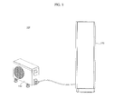
- FIG. 1 is a perspective view illustrating a configuration of an air conditioner in accordance with a preferred embodiment of the present invention
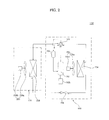
- FIG. 2 is a schematic view illustrating the air conditioner in FIG. 1 .
- the air conditioner 100 includes an outdoor unit 150 and an indoor unit 170.
- the outdoor unit 150 is operated in a cooling mode or a heating mode for supplying refrigerant to the indoor unit 170 in response to demand from the indoor unit 170 connected thereto or an external control order.
- the outdoor unit 150 includes a compressor 152 for compressing the refrigerant, a compressor motor 152b for driving the compressor, an outdoor heat exchanger 154 for dissipating heat from compressed refrigerant, an outdoor fan unit 155 having an outdoor fan 155a arranged to one side of the outdoor heat exchanger 154 for accelerating the heat dissipation from the refrigerant and a motor 5b for rotating the outdoor fan 155a, an expansion device 156 for expanding condensed refrigerant, a cooling/heating change-over valve 160 for changing a flow path of the compressed refrigerant, and an accumulator 153 for temporary storage of gas refrigerant for supplying refrigerant at a fixed pressure to the compressor after removal of water and foreign matter from the refrigerant.
- the compressor 152 may be one of an inverter compressor, and a constant speed compressor.
- the outdoor unit 150 may further include at least one pressure sensor (Not shown) for measuring a pressure of the refrigerant, and at least one temperature sensor (Not shown) for measuring a temperature.
- the indoor unit 170 includes an indoor heat exchanger 208 arranged to a room for cooling or heating a room, and an indoor fan unit 209 having an indoor fan 209a arranged to one side of the indoor heat exchanger 208 for accelerating heat dissipation from the refrigerant, and a motor 209b for rotating the indoor fan 209a.
- the indoor unit 170 may further include an outlet (Not shown) for discharging heat exchanged air, and a wind direction controller (Not shown) for controlling opening/closing of the outlet (Not shown) and a direction of the air being discharged.
- a vane may be mounted for opening/closing at least one of an air inlet (Not shown) and the air outlet (Not shown) as well as guiding the air. The vane may, not only open/close the air inlet and the air outlet, but also guide a direction of the air being drawn in or discharged.
- the indoor unit 170 may control an air flow rate being drawn in or discharged by controlling a rotation speed of the indoor fan 209a.
- the indoor unit 170 may further include a display unit (Not shown) for displaying an operation state and information set to the indoor unit 170, and an input unit (Not shown) for inputting data to be set. Also, the indoor unit 170 may further include an indoor temperature sensing unit (Not shown) for sensing a room temperature, and a human body sensing unit (Not shown) for sensing a human body present to a room space.
- the air conditioner 100 may be configured as a room cooler for cooling the room, or as a heat pump for cooling or heating the room.
- the indoor unit 170 taking a stand type as an example, a ceiling type or a wall mounting type may also viable, or a variety of modes, such as a unit type which has no individual outdoor unit or an indoor unit, may also viable.
- refrigerant pipelines are connected between the indoor unit 170 and the outdoor unit 150, for discharging refrigerated/heated air to the room from the indoor unit 170 depending on circulation of the refrigerant.
- the one outdoor unit 150 may be connected to a plurality of the indoor units 170, or at least one indoor unit may be connected to each of a plurality of the outdoor units.
- the indoor unit 170 and the outdoor unit 150 may have communication lines connected therebetween for transmission/reception of a control order according to a predetermined communication system.
- the compressor 152 may be driven by drive power supplied thereto through a power converter 200.
- the drive power may be supplied to the motor in the compressor 152 from the power converter 200.
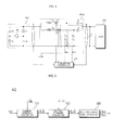
- FIG. 3 is a block diagram illustrating the power converter in the outdoor unit in FIG. 1
- FIG. 4 is a circuit diagram illustrating the converter in the power converter in FIG. 3 .
- the power converter 200 in accordance with a preferred embodiment of the present invention may include a filter unit 403, a rectifying unit 405, a converter 410, a converter controller 415, a capacitor C, an inverter 420, and an inverter controller 430.
- the filter unit 403 may be arranged between an input AC power source 201 and the rectifying unit 405, for filtering out a harmonic current from the input AC power source 201 or the power converter 200.
- the filter unit 403 may have an inductor which is an inductive device, and a capacitor which is a capacitive device.
- the filter unit 403 may have an LCL filter with the inductor, the capacitor and the inductor.
- the rectifying unit 405 receives the input AC power 201 from the filter unit 403 and rectifies the same. Though FIG. 4 illustrates the rectifying unit 405 for single phase AC power, having four diodes Da, Db, Dc, and Db used in a bridge mode, a variety of embodiments are viable.
- the converter 410 converts the power rectified at the rectifying unit 405 to DC power and outputs the same. Particularly, the converter 410 outputs the DC power to a capacitor C arranged at output terminals of the converter 410.
- the embodiment of the present invention suggests using an interleave converter (Cascade converter) having a plurality of converters 410a, 410b, ---- as the converter 410.
- an interleave boost converter, an interleave buck boost converter, an interleave buck converter and so on are viable as the interleave converter, the specification will be described focused on the interleave boost converter.
- the plurality of boost converters 410a, 410b, ---- in the interleave boost converter 410 are connected in parallel, for performing interleaved operation.
- a first boost converter 410a and a second boost converter 410b connected in parallel to each other in the interleave boost converter 410 perform interleaved operation
- a first switching element S1 in the first boost converter 410a and a second switching element S2 in the second boost converter 410b are turned on/off with a 180degree phase difference from each other electrically, a switching loss takes place, consequently.
- the switching loss taken place thus performs efficiency at a low load region lower than efficiency at a high load region.
- the embodiment of the present invention suggests changing a number of operating interleaved converters according to a load level of both terminals of the capacitor which are output terminals of the interleaved converters for increasing operation efficiency of entire region.
- the interleave converter 410 is controlled such that the first boost converter 410a is operated at the low load region, and the first boost converter 410a and the second boost converter 410b are operated at the high load region.
- the interleave convertor 410 of such a configuration is illustrated in FIG. 4 .
- an MOSFET metal oxide semiconductor field effect transistor
- IGBT insulated gate bipolar mode transistor
- the boost converters 410a, 410b, ---- in the interleave converter 410 may be embodied of, but not limited to, the same type switching elements, for an example, the MOSFET or IGBT, other types of switching elements may also used.
- the MOSFET device may be used for the first boost converter 410a
- the IGBT device may be used for the second boost converter 410b.
- the interleave converter 410 may perform stable operation.
- FIG. 4 illustrates the first boost converter 410a and the second boost converter 410b.
- the boost converter 410 will be described focused on the first boost converter 410a and the second boost converter 410b.
- the first boost converter 410a may include a first diode D1 having one terminal connected to the capacitor C, a first inductor L1 connected between the first diode D1 and the rectifying unit 405, and a first boost switching element S1 connected to the first inductor L1 and the first diode D1 in parallel.
- the second boost converter 410b may include a second diode D2 having one terminal connected to the capacitor C, a second inductor L2 connected between the second diode D2 and the rectifying unit 405, and a second boost switching element S2 connected to the second inductor L2 and the second diode D2 in parallel.
- first boost converter 410a and the second boost converter 410b connected to each other in parallel to perform interleaved operation, performing the first switching element S1 in the first boost converter 410a and the second switching element S2 in the second boost converter 410b to be turned on/off with a 180degree phase difference electrically, a switching loss takes place, accordingly.
- the switching loss taken place in this time performs efficiency at the low load region lower than efficiency at the high load region.
- the embodiment of the present invention suggests changing a number of operating converters in the interleave converter according to a load level on the both terminals of the capacitor which are output terminals of the interleave converter 410, thereby improving operation efficiency for entire load regions.
- the interleave converter 410 is controlled such that the first boost converter 410a is operated in the low load region, and the first boost converter 410a and the second boost converter 410b are operated in the high load region.
- the converter controller 415 divides a load region into the low load region Ae1 (See FIG. 6A ) and the high load region Ae2 (See FIG. 6A ) according to a load of a voltage at the both terminals of the capacitor C to control the interleave converter 410 such that only the first boost switching element S1 in the first converter 410a is operated in the low load region, and the first boost switching element S1 and the second boost switching element S2 are operated alternately such that the first converter 410a and the second converter 410b perform interleaved operation in the high load region.
- first converter 410a and the second converter 410b are connected in parallel to each other and operable in boost modes.
- the boost mode operation will be described in detail later, with reference to FIGS. 8A and 8B .
- first boost switching element S1 in the first boost converter 410a and the second boost switching element S2 in the second boost converter 410b may be identical switching elements, for an example, the MOSFET or the IGBT.
- first boost switching element S1 in the first boost converter 410a and the second boost switching element S2 in the second boost converter 410b may also be switching elements different from each other.
- the first boost switching element S1 in the first boost converter 410a may be the MOSFET for performing high efficiency power conversion
- the second boost switching element S2 which is operated in the high load region may be the IGBT.
- the power converter 200 may further include an input voltage detector A for detecting an output terminal voltage of the rectifying unit 405, an output voltage detector B for detecting an output terminal voltage of the interleave boost converter 410, i.e., a voltage of a DC terminal capacitor C, and a current detector F1 and F2 for detecting a current flowing to the inductor L1 and L2 in the interleave boost converter 410.
- an input voltage detector A for detecting an output terminal voltage of the rectifying unit 405
- an output voltage detector B for detecting an output terminal voltage of the interleave boost converter 410, i.e., a voltage of a DC terminal capacitor C
- a current detector F1 and F2 for detecting a current flowing to the inductor L1 and L2 in the interleave boost converter 410.
- the input voltage detector A may detect an output terminal voltage of the rectifying unit 405.
- the input voltage detector A may include a resistor device, an amplifier, and so on.
- An input voltage Vc1 to be detected being a pulse mode discrete signal, may be inputted to the convertor controller 415.
- the output voltage detector B i.e., the DC terminal voltage detector B may detect an output terminal voltage of the interleave boost converter 410, particularly, an opposite terminal voltage Vdc of the capacitor C.
- the capacitor C is arranged between the inverter 420 and the load 205 for storing an output DC power of the interleave converter thereto.
- the drawing illustrates one device as the smoothing capacitor C, a plurality of devices may be provided for securing device stability.
- the both terminals of the capacitor C may be named as DC terminals or DC link terminals.
- the load is defined to include the inverter 420 and the motor 205, it may be shown that the load 205 is connected to the both terminals of the capacitor C in the power converter as shown in the drawing. According to this, the DC terminal voltage Vdc may be the same with a load 205 voltage.
- the output voltage Vdc to be detected being a pulse mode discrete signal, may be inputted to the converter controller 415.
- the first current detector F1 may detect a current i L1 flowing to the first inductor L1 in the first boost converter 410a
- the second current detector F2 may detect a current i L2 flowing to the second inductor L2 in the second boost converter 410b.
- CTS Current Transformers
- shunt resistors and the like may be used as the first and second current detectors F1 and F2.
- the input AC current i L1 , and i L2 to be detected, being pulse mode discrete signals, may be inputted to the converter controller 415.
- the converter controller 415 may include a first converter controller (Not shown) for controlling the first boost converter 410a, and a second converter controller (Not shown) for controlling the second boost converter 410b.
- the converter controller 415 may calculate the load on the both terminals of the capacitor based on at least one of the first and second input currents i L1 and i L2 detected by the first and second current detectors F1 and F2 and the DC terminal voltage Vdc detected by the DC terminal voltage detector B. And, if the calculated load falls under the low load region, the converter controller 415 may control a turn on/turn off timing of the first boost switching element S1 in the first boost converter 410a.
- the converter controller 415 may control to operate both the first and second boost converters 410a and 410b. That is, the converter controller 415 may control a turn on/turn off timing of the first boost switching element S1 in the first boost converter 410a, and a turn on/turn off timing of the second boost switching element S2 in the second boost converter 410b. In this case, the first boost converter 410a and the second boost converter 410b may perform interleaved operation.
- the inverter 420 has a plurality of inverter switching elements for converting the DC current Vdc smoothened by the turn on/turn off operation of the switching element into a three phase power va, vb, and vc of a predetermined frequency and outputting the same to a three phase synchronous motor 250.
- the motor 250 may be a motor in the compressor.
- the inverter controller 430 outputs an inverter switching control signal Sic to the inverter 420 for controlling switching operation of the inverter 420.
- the inverter switching control signal Sic being a PWM switching control signal, is generated and output based on an output current value i 0 detected by the output current detector (E in FIG. 9 ).
- FIG. 5 is a block diagram illustrating the converter controller 415 in FIG. 4 .
- the converter controller 415 may include a current command generator 510, a voltage command generator 520, and a switching control signal output unit 530.
- the current command generator 510 may generate d-, q-axis current command value i*d, i*q with a PI controller or the like based on the DC terminal voltage Vdc detected by the output voltage detector B, i.e., the DC terminal voltage detector B and a DC terminal voltage command value V*dc.
- the voltage command generator 520 generates d-, q-axis voltage command value v* d , v* q with the PI controller or the like based on the d-, q-axis current command value i*d, i*q and the first and the detected second input currents i L1 , iL 2 .
- the switching control signal output unit 530 outputs a first converter switching control signal Scc1 and a second converter switching control signal Scc2 to the first boost converter 410a and the second boost converter 410b respectively for driving the first boost switching element S1 in the first boost converter 410a and the second boost switching element S2 in the second boost converter 410b based on the d-, q-axis voltage command value v* d , v* q .
- the converter controller 415 calculates the load based on the DC terminal voltage Vdc detected by the DC terminal voltage detector B and the first input current i L1 and the second input current i L2 detected by the first current detector F1 and the second current detector F2, and outputs the first converter switching control signal Scc1 to the first boost converter 410a for driving the first switching element S1 if the calculated load falls under the low load region.
- the converter controller 415 outputs the first converter switching control signal Scc1 and the second converter switching control signal Scc2 to the first boost converter 410a and the second boost converter 410b respectively for interleaved driving of the first switching element S1 and the second switching element S2.
- FIG. 6A is a graph illustrating load regions of a power converter.
- the converter controller 415 may calculate the load on the both terminals of the capacitor based on at least one of the first and second input currents i L1 and i L2 detected by the first and second current detectors F1 and F2 and the DC terminal voltage Vdc detected by the DC terminal voltage detector B.
- the load may be electric power.
- the converter controller 415 may determine that the load is a low load if the calculated load is lower than a first electric power level Px, and the load is a high load if the calculated load is higher than the first electric power level Px. Or, the converter controller 415 may determine that the load is a low load if the calculated load is lower than the first electric power level Px, and the load is a high load if the calculated load is higher than a second electric power level which is higher than the first electric power level Px.
- the load 205 may be divided into a low load region Ae1, and a high load region Ae2.
- the first electric power level Px may be stored in a memory (Not shown) in the power converter 200.
- the first electric power level Px is variable with an operation condition, and the like. For an example, if a highest load used for a predetermined time period is below a predetermined value, the first electric power level Px may be lowered.
- FIG. 6B is a graph illustrating power vs. power factor of respective regions in FIG. 6A .
- a load lower than the first electric power level Px may fall under the low load region Ae1, and a load higher than the first electric power level Px may fall under the high load region Ae2.
- load vs. operation efficiency (Power factor) may be illustrated as an LP1 curve
- load vs. operation efficiency may be illustrated as an LP2 curve
- the operation efficiency is low due to a switching loss in the low load region, and, if only the first boost converter 410a is in operation, the operation efficiency is low in the high load region.
- the interleave boost converter is controlled such that only the first boost converter 410a is operated in the low load region with reference to the first electric power level Px, and both the first and second boost converters 410a and 410b are operated in the high load region with reference to the first electric power level Px.
- the operation efficiency of the rectifier 200 can be improved in comparison to the load. Especially, the operation efficiency can be improved for a whole load region.
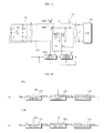
- FIGS. 7A and 7B are circuit diagrams illustrating operation of the power converter in FIG. 4 , respectively.
- FIG. 7A illustrates operation of only the first boost converter 410a in the low load region.
- the converter controller 415 may control to operate only the first boost converter 410a.
- the first boost switching element S1 in the first boost converter 410a is turned on by the first converter switching control signal Scc1 from the converter controller 415. According to this, a current is accumulated at the first inductor for outputting energy accumulated in the first inductor to the capacitor C when the first boost switching element S1 is turned off.
- the switching loss can be reduced, and, by performing only the first boost switching element S1 to be in operation, since an output DC voltage can be lowered further, the operation efficiency can be improved.
- FIG. 7B illustrates operation of the first boost converter 410a and the second boost converter 410b in the high load region.
- the converter controller 415 may control the first boost converter 410a and the second boost converter 410b to perform interleaved operation.
- the first boost switching element S1 in the first boost converter 410a is turned on by the first converter switching control signal Scc1 from the converter controller 415.
- the second boost switching element S2 in the second boost converter 410b may be turned off.
- the second boost switching element S2 in the second boost converter 410b is turned on by the second converter switching control signal Scc2 from the second converter controller 415b.
- the first boost converter 410a and the second boost converter 410b can perform interleaved operation when the load is high.
- the input current ripple and noise can be reduced.
- the operation efficiency can be improved even in the high load region.
- FIGS. 8A and 8B are reference circuit diagrams for describing operation of the first converter in FIG. 4 .
- FIGS. 8A and 8B illustrate the first boost converter 410a operated in a boost mode.
- FIG. 8A illustrates a current Ia flowing to a closed loop constructed of the first inductor L1 and the first boost switching element S1 if the first boost switching element S1 in the first boost converter 410a is turned on. According to this, energy is accumulated at the first inductor L1 based on the current Ia. In this case, the first diode D1 is not conductive.
- FIG. 8B illustrates the first diode D1 become conductive if the first boost switching element S1 in the first boost converter 410a is turned off to perform a current Ib to flow through the first inductor L1 and the first diode D1.
- the current Ib may be a sum of the energy accumulated at the first inductor L1 in FIG. 8A and the current based on the input AC power source 201.
- the first boost switching element S1 in the first boost converter 410a is turned on/off, i.e., pulse width modulated.
- FIG. 9 illustrates an inverter circuit in the power converter in FIG. 3 .
- the inverter 420 has upper switching elements Sa, Sb, Sc connected in series and lower switching elements S'a, S'b, S'c connected in series, which construe one pair, to have total three pairs of upper and lower switching elements Sa&S'a, Sb&S'b, Sc&S'c connected in parallel to each other.
- Each of the switching elements Sa, S'a, Sb, S'b, Sc. S'c has a diode connected thereto in an antiparallel.
- the switching elements in the inverter 420 are turned on/off in response to a switching control signal Sic from the controller 430.
- the inverter 420 converts the DC current to the both terminals of the capacitor C into an AC current for driving the motor 250.
- the inverter controller 430 may control operation of the switching element in the inverter 420. For this, the inverter controller 430 may receive the output current i 0 from the output current detector (E in FIG. 9 ).
- the inverter controller 430 outputs the inverter switching control signal Sic to the inverter 420 for controlling switching operation of the inverter 420.
- the inverter switching control signal Sic being a PWM switching control signal, is generated and output based on the output current value i 0 from the output current detector (E in FIG. 9 ).
- the output current detector (E in FIG. 9 ) may detect the output current i 0 flowing between the inverter 420 and the three phase motor 250, i.e., a current flowing to the motor 250.
- the output current detector E may detect entire output currents ia, ib, ic of respective phases, or the output currents of two phases by using three phase equilibrium.
- the output current detector E may be positioned between the inverter 420 and the motor 250, and a CT (Current Transformer) or a shunt resistor may be used for detection of the current.
- CT Current Transformer
- three shunt resistors may be positioned between the inverter 420 and the synchronous motor 250, or may have one terminals connected to the three lower arm switching elements S'a, S'b, S'c, respectively.
- use of two shunt resistors by using the three phase equilibrium is also viable.
- one shunt resistor is used, it is viable that the shunt resistor is arranged between the capacitor C and the inverter 420.
- the detected output current i o being a pulse mode discrete signal, may be applied to the controller 430, and the inverter switching control signal Sic is generated based on the detected output current i o . Description hereinafter will be made assuming that the detected output current i o is the three phase output currents ia, ib. ic.
- FIG. 10 is a block diagram illustrating the inverter controller in FIG. 9 .
- the inverter controller 430 may include a axis transformation unit 310, a speed calculator 320, a current command generator 330, a voltage command generator 340, a axis transformation unit 350, and a switching control signal output unit 360.
- the axis transformation unit 310 receives the three phase output current ia, ib, ic from the output current detector E and converts the three phase output currents ia, ib, ic into two phase currents i ⁇ , i ⁇ on a rest frame.
- the axis transformation unit 310 may convert the two phase currents i ⁇ , i ⁇ on the rest frame into two phase currents id, iq on a rotary coordinate system.
- the speed calculator 320 may calculate speed ( ⁇ r based on a position signal H of a rotor received from a position sensing unit 235. That is, the speed may be obtained by dividing the position signal with a time period.
- the position sensing unit 235 may sense a position of the rotor of the motor 250.
- the position sensing unit 235 may include a hole sensor.
- the speed calculator 320 may output a calculated position ⁇ r and a calculated speed ⁇ r based on the position signal H of the rotor applied thereto.
- the current command generator 330 calculates a speed command value ⁇ * r based on the calculated speed ⁇ r and a target speed ⁇ , and generates a current command value i* q based on the speed command value ⁇ * r .
- the current command generator 330 performs PI control at a PI controller 535 based on the speed command value ⁇ * r which is a difference between the calculated speed ⁇ r and a target speed ⁇ to generate the current command value i* q .
- the drawing illustrates a q-axis current command value i* q as the current command value, different from the drawing, a d-axis current command value i * d may also be generated, altogether.
- a value of the d-axis current command value i * d may be set to be zero.
- the current command generator 330 may further include a limiter (Not shown) for limiting a level of the current command value i* q so that the current command value i* q does not exceed an allowable range.
- a limiter (Not shown) for limiting a level of the current command value i* q so that the current command value i* q does not exceed an allowable range.
- the voltage command generator 340 generates d-axis, q-axis voltage command values v* d , v* q based on the d-axis, q-axis currents i d , iq pivoted to the two phase rotary coordinate system at the axis transformation unit and the current command values i*d, i* q from the current command generator 330 and the like.
- the voltage command generator 340 may perform PI control at the PI controller 544 and may generate a q-axis voltage command value v* q based on a difference between the q-axis current iq, and the q-axis current command value i* q .
- the voltage command generator 340 may perform PI control at the PI controller 548, and may generate the d-axis voltage command value v * d based on a difference between the d-axis current i d and the d-axis current command value i * d .
- a value of the d-axis voltage command value v* d may be set to zero matched to a case in which the d-axis current command value i * d is set to zero.
- the voltage command generator 340 may further include a limiter (Not shown) for limiting a level of the d-, q-axes voltage command values v* d , v* q so that the d-, q-axes voltage command values v* d , v* q do not exceed allowable ranges, respectively.
- a limiter (Not shown) for limiting a level of the d-, q-axes voltage command values v* d , v* q so that the d-, q-axes voltage command values v* d , v* q do not exceed allowable ranges, respectively.
- the axis transformation unit 350 receives the position ⁇ r from the speed calculator 320 and the d-, q-axes voltage command values v* d , v* q and performs pivoting.
- the axis transformation unit 350 performs pivoting from the two phase rotary coordinate system to the two phase rest frame.
- the position ⁇ r calculated at the speed calculator 320 may be used.
- the axis transformation unit 350 may perform pivoting from the two phase rest frame to a three phase rest frame. With such pivoting, the axis transformation unit 350 outputs three phase output voltage command values v*a, v*b, v*c.
- the switching control signal output unit 360 generates and outputs a PWM inverter switching control signal Sic based on the three phase output voltage command values v*a, v*b, v*c.
- the inverter switching control signal Sic may be converted into a gate drive signal at a gate drive unit (Not shown) and applied to gates of respective switching elements in the inverter 420. According to this, the switching elements Sa, S'a, Sb, S'b, Sc, S'c in the inverter 420 perform switching operation.
- FIG. 11 An interleave converter of such a configuration is illustrated in FIG. 11 .
- FIG. 11 is another exemplary circuit diagram illustrating the converter in the power converter in FIG. 3 .
- FIG. 11 illustrates the first boost converter 410a and the second boost converter 410b.
- the boost converter will be described taking the first boost converter 410a and the second boost converter 410b as an example.
- the first boost converter 410a may include a first diode D1 having one terminal connected to the capacitor C, a first inductor L1 connected between the first diode D1 and the rectifying unit 405, and a first boost switching element S1 connected to the first inductor L1 and the first diode D1 in parallel.
- the first boost switching element S1 may be an MOSFET switching element.
- the second boost converter 410b may include a second diode D2 having one terminal connected to the capacitor C, a second inductor L2 connected between the second diode D2 and the rectifying unit 405, and a second boost switching element S2 connected to the second inductor L2 and the second diode D2 in parallel.
- the second boost switching element S2 may be an IGBT switching element.
- the MOSFET switching element has advantages of fast operation speed and good power rectifying efficiency, the MOSFET switching element has a drawback of limitation of use at the high load region due to a rated voltage lower than the IGBT switching element.
- the IGBT switching element has a high rated voltage enabling to perform stable operation at a load region higher than the MOSFET switching element, the IGBT switching element has a drawback in that power rectifying efficiency is poor due to an operation speed lower than the MOSFET switching element.
- the power converter is used in the compressor of the air conditioner which has large variation of the load, and if any one of the switching elements is used selectively, it may be difficult to perform operation which satisfies both the low load region and the high load region.
- the present invention suggests using both the MOSFET switching element and the IGBT switching element.
- the interleave converter is used for operating respective switching elements depending on the load.
- the converter controller 415 divides the load of the voltage at both terminals of the capacitor C into a low load region Ae1 (See FIG. 13 ), a high load region Ae3 (See FIG. 13 ), and an intermediate load region Ae2 (See FIG. 13 ), and, according to the load regions, controls to operate only the MOSFET switching element S1 in the first boost converter 410a at the low load region, controls to operate only the IGBT switching element S2 in the second boost converter 410b at the high load region, and controls the MOSFET switching element S1 and the IGBT switching element S2 alternately such that the first boost converter 410a and the second boost converter 410b perform interleaved operation at the intermediate region.
- the first boost converter 410a and the second boost converter 410b are connected to each other in parallel, and operable in a boost mode.
- the boost mode operation will be described later with reference to FIGS. 15A and 15B .
- the power converter 200 may further include an input voltage detector A for detecting an output terminal voltage of the rectifying unit 405, an output voltage detector B for detecting an output terminal voltage of the interleave boost converter 410, i.e., a voltage of a DC terminal capacitor C, and a current detector F1 and F2 for detecting a current flowing to the inductor L1 and L2 in the interleave boost converter 410.
- an input voltage detector A for detecting an output terminal voltage of the rectifying unit 405
- an output voltage detector B for detecting an output terminal voltage of the interleave boost converter 410, i.e., a voltage of a DC terminal capacitor C
- a current detector F1 and F2 for detecting a current flowing to the inductor L1 and L2 in the interleave boost converter 410.
- the input voltage detector A may detect an output terminal voltage of the rectifying unit 405.
- the input voltage detector A may include a resistor device, an amplifier, and so on.
- An input voltage Vc1 to be detected being a pulse mode discrete signal, may be inputted to the convertor controller 415.
- the output voltage detector B i.e., the DC terminal voltage detector B may detect an output terminal voltage of the interleave boost converter 410, particularly, an opposite terminal voltage Vdc of the capacitor C.
- the capacitor C is arranged between the inverter 420 and the load 205 for storing an output DC power of the interleave converter thereto.
- the drawing illustrates one device as the smoothing capacitor C, a plurality of devices may be provided for securing device stability.
- the both terminals of the capacitor C may be named as DC terminals or DC link terminals.
- the load is named to include the inverter 420 and the motor 205, it may be shown that the load 205 is connected to the both terminals of the capacitor C in the power converter as shown in the drawing. According to this, the DC terminal voltage Vdc may be the same with a load 205 voltage.
- the output voltage Vdc to be detected being a pulse mode discrete signal, may be inputted to the converter controller 415.
- the first current detector F1 may detect a current i L1 flowing to the first inductor L1 in the first boost converter 410a
- the second current detector F2 may detect a current i L2 flowing to the second inductor L2 in the second boost converter 410b.
- CTS Current Transformers
- shunt resistors and the like may be used as the first and second current detectors F1 and F2.
- the input AC currents i L1 , and i L2 to be detected, being pulse mode discrete signals, may be inputted to the converter controller 415.
- the converter controller 415 may have a first converter controller 415a for controlling the first boost converter 410a, and a second converter controller 415b for controlling the second boost converter 410b.
- the first converter controller 415a may calculate the load based on the DC terminal voltage Vdc sensed at the output voltage detector B, and the first inductor current I L1 detected at the first current detector F1.
- the first converter controller 415a may control a turn on/turn off timing of the MOSFET switching element S1 in the first boost converter 410a if the calculated load falls under the low load region.
- the first converter controller 415a may output the calculated load to the second converter controller 415b.
- the second converter controller 415b may control a turn on/turn off timing of the IGBT switching element S2 in the second boost converter 410b.
- the first converter controller 415a may control a turn on/turn off timing of the MOSFET switching element S1 in the first boost converter 410a, and may output the calculated load to the second converter controller 415b.
- the second converter controller 415b may control a turn on/turn off timing of the IGBT switching element S2 in the second boost converter 410b.
- the second converter controller 415b may also calculate the load based on the DC terminal voltage Vdc sensed at the output voltage detector B and the second inductor current I L2 detected at the second current detector F2. And, if the calculated load falls under the high load region, the second converter controller 415 may control the turn on/turn off timing of the IGBT switching element S2 in the second boost converter 410b.
- the inverter 420 has a plurality of inverter switching elements for converting the DC current Vdc smoothened by the turn on/turn off operation of the switching element into a three phase power va, vb, and vc of a predetermined frequency and outputting the same to a three phase synchronous motor 250.
- the motor 250 may be a motor in the compressor.
- the inverter controller 430 outputs an inverter switching control signal Sic to the inverter 420 for controlling switching operation of the inverter 420.
- the inverter switching control signal Sic being a PWM switching control signal, is generated and output based on an output current value i o detected by the output current detector (E in FIG. 9 ).
- FIGS. 12A and 12B are block diagrams illustrating the converter controllers in FIG. 11 , respectively.
- FIG. 12A illustrates a block diagram of the first converter controller 415a in FIG. 11 .
- the first converter controller 415a may include a current command generator 330, a voltage command generator 320, and a switching control signal output unit 330.
- the current command generator 330 may generate a d-, q-axis current command value i* d1 , i* q1 with the PI controller or the like based on the DC terminal voltage Vdc detected by the output voltage detector B, i.e., the DC terminal voltage detector B and the DC terminal voltage command value V*dc.
- the voltage command generator 320 generates d-, q-axis voltage command value v* d1 , v* q1 with the PI controller or the like based on the d-, q-axis current command value i* d1 , i* q1 and the detected first input current i L1 .
- the switching control signal output unit 330 outputs a first converter switching control signal Scc1 to the first boost converter 410a for driving the MOSFET switching element S1 in the first boost converter 410a based on the d-, q- axis voltage command value v* d1 , v* q1 .
- the first converter controller 415a outputs the first converter switching control signal Scc1 to the first boost converter 410a for driving the first switching element S1 if the calculated load falls under the low load region based on the DC terminal voltage Vdc detected by the DC terminal voltage detector B, and the first input current i L1 detected by the first current detector F1.
- FIG. 12B illustrates a block diagram of the second converter controller 415b in FIG. 11 .
- the second converter controller 415b may include a current command generator 315, a voltage command generator 325, and a switching control signal output unit 335.
- the current command generator 315 may generate a d-, q-axis current command value i* d2 , i* q2 with the PI controller or the like based on the DC terminal voltage Vdc detected by the output voltage detector B, i.e., the DC terminal voltage detector B and the DC terminal voltage command value V*dc.
- the voltage command generator 325 generates a d-, q-axis voltage command value v* d2 , v* q2 with the PI controller or the like based on the d-, q-axis current command value i* d2 , i* q2 and the detected second input current i L2 .
- the switching control signal output unit 335 outputs a second converter switching control signal Scc2 to the second boost converter 410b for driving the IGBT switching element S2 in the second boost converter 410b based on the d-, q- axis voltage command value v* d2 , v* q2 .
- the second converter controller 415b outputs the second converter switching control signal Scc2 to the second boost converter 410b for driving the IGBT switching element S21 based on the DC terminal voltage Vdc detected by the DC terminal voltage detector B, and the second input current i L2 detected by the second current detector F2.
- FIG. 13 is a graph illustrating load regions of a power converter.
- the first converter controller 415a or the second converter controller 415b may calculate the load on the both terminals of the capacitor based on the DC terminal voltage Vdc detected by the DC terminal voltage detector B and the first and second input currents i L1 and i L2 detected by the first and second current detectors F1 and F2.
- the load may be electric power.
- the first converter controller 415a or the second converter controller 415b may determine that the load is a low load if the calculated load is lower than a first electric power level Pa, a high load if the calculated load is higher than a second electric power level Pb, and an intermediate load if the calculated load falls between the first electric power level Pa and the second electric power level Pb.
- the load may be divided into a low load region Ae1, an intermediate load region Ae2, and a high load region Ae3.
- the first electric power level Pa and the second electric power level Pb may be stored in a memory (Not shown) in the power converter 200.
- the first electric power level Pa and the second electric power level Pb may be variable with an operation condition, and the like. For an example, if a highest load used for a predetermined time period is below a predetermined value, the first electric power level Pa and the second electric power level Pb may be lowered.
- FIGS. 14A to 14C are circuit diagrams illustrating operation of the power converter in FIG. 11 , respectively.
- FIG. 14A illustrates operation of only the first boost converter 410a in the low load region.
- the first converter controller 415a or the second converter controller 415b may control to operate only the first boost converter 410a.
- the MOSFET switching element S1 in the first boost converter 410a is turned on by the first converter switching control signal Scc1 from the first converter controller 415a. According to this, a current is accumulated at the first inductor for outputting energy accumulated in the first inductor to the capacitor C when the MOSFET switching element S1 is turned off.
- FIG. 14B illustrates operation of the first boost converter 410a and the second boost converter 410b in the intermediate load region.
- the first converter controller 415a or the second converter controller 415b may determine that the load is the intermediate load, to control the first boost converter 410a and the second boost converter 410b to perform interleaved operation.
- the MOSFET switching element S1 in the first boost converter 410a is turned on in response to the first converter switching control signal Scc1 from the first converter controller 415a.
- the IGBT switching element S2 in the second boost converter 410b may be turned off.
- the IGBT switching element S2 in the second boost converter 410b is turned on in response to the second converter switching control signal Scc2 from the second converter controller 415b.
- the input current ripple and noise can be reduced.
- FIG. 14C illustrates operation of only the second boost converter 410b in the high load region.
- the first converter controller 415a or the second converter controller 415b may control to operate only the second boost converter 410b.
- the IGBT switching element S2 in the second boost converter 410b is turned on by the second converter switching control signal Scc2 from the second converter controller 415b. According to this, a current is accumulated at the second inductor L2 for outputting energy accumulated in the second inductor to the capacitor C when the IGBT switching element S2 is turned off.
- FIGS. 15A and 15B are reference circuit diagrams for describing operation of the first converter in FIG. 11 .
- FIGS. 15A and 15B illustrate the first boost converter 410a operated in a boost mode.
- FIG. 15A illustrates a current Ia flowing to a closed loop constructed of the first inductor L1 and the first boost switching element S1 if the first boost switching element S1 in the first boost converter 410a is turned on.
- the first diode D1 is not conductive.
- FIG. 15B illustrates the first diode D1 become conductive if the first boost switching element S1 in the first boost converter 410a is turned off to perform a current Ib to flow through the first inductor L1 and the first diode D1.
- the current Ib may be a sum of the energy accumulated at the first inductor L1 and the current based on the input AC power source 201.
- the first boost switching element S1 in the first boost converter 410a is turned on/off, i.e., pulse width modulated.
- the power converter and the air conditioner having the same of the present invention have the following advantages.
- the power converter and the air conditioner having the same includes the interleave converter in which the converter controller changes a number of operating converters in the interleave converter based on a load level of both terminals of the capacitor, permitting to enhance operation efficiency, not only at the low load region, but also at the high load region, and active variation of the output voltage of the interleave converter with variation of the load level of the both terminals of the capacitor which are output terminals of the interleave converter, to enhance operation efficiency throughout entire load region, enabling to drive a compressor or the like having a large variation of the load, efficiently.
- control to operate only the first converter in the interleave converter if the load level of the both terminals of the capacitor is lower the first level enables to enhance the operation efficiency by removing the switching loss caused by the second converter, and, moreover, lower the DC power further enabling to enlarge a width of the DC terminal voltage at the both terminals of the capacitor.
- the interleaved operation of the first converter and the second converter enables to reduce the input current ripple and the noise.
- the power converter and the air conditioner having the same includes the interleave converter in which the first converter includes a first switching element of a first type and the second converter includes a second switching element of a second type having a rated voltage higher than the first type, thereby permitting to operate the switching elements matched to a variety of loads.
- the operation efficiency can be improved, and by operating the second switching element having a high rated voltage in the high load, stable operation is possible in the high load, too.
- the interleaved operation of the first converter and the second converter in the intermediate load enables to reduce the input current ripple and the nose.
- the method for operating the power converter and an air conditioner according to the foregoing embodiments may be implemented as code that can be written to a processor-readable recording medium included in the charging apparatus and can thus be read by a processor.
- the processor-readable recording medium may be any type of recording device in which data can be stored in a processor-readable manner.
Landscapes
- Engineering & Computer Science (AREA)
- Power Engineering (AREA)
- Dc-Dc Converters (AREA)
- Inverter Devices (AREA)
- Rectifiers (AREA)
Applications Claiming Priority (2)
| Application Number | Priority Date | Filing Date | Title |
|---|---|---|---|
| KR1020130026866A KR102058042B1 (ko) | 2013-03-13 | 2013-03-13 | 전력변환장치, 및 이를 구비하는 공기조화기 |
| KR1020130026865A KR20140112297A (ko) | 2013-03-13 | 2013-03-13 | 전력변환장치, 및 이를 구비하는 공기조화기 |
Publications (3)
| Publication Number | Publication Date |
|---|---|
| EP2779406A2 true EP2779406A2 (fr) | 2014-09-17 |
| EP2779406A3 EP2779406A3 (fr) | 2015-08-26 |
| EP2779406B1 EP2779406B1 (fr) | 2022-02-23 |
Family
ID=50241221
Family Applications (1)
| Application Number | Title | Priority Date | Filing Date |
|---|---|---|---|
| EP14159054.7A Active EP2779406B1 (fr) | 2013-03-13 | 2014-03-12 | Convertisseur de puissance et climatiseur comportant celui-ci |
Country Status (3)
| Country | Link |
|---|---|
| US (1) | US9742336B2 (fr) |
| EP (1) | EP2779406B1 (fr) |
| CN (1) | CN104052274B (fr) |
Cited By (1)
| Publication number | Priority date | Publication date | Assignee | Title |
|---|---|---|---|---|
| EP3229368A4 (fr) * | 2014-12-01 | 2017-12-20 | Samsung Electronics Co., Ltd. | Dispositif d'entraînement de moteur, climatiseur le comprenant et son procédé de commande |
Families Citing this family (17)
| Publication number | Priority date | Publication date | Assignee | Title |
|---|---|---|---|---|
| JP2014187764A (ja) * | 2013-03-22 | 2014-10-02 | Toshiba Corp | 電圧変換回路および切替制御回路 |
| KR101655625B1 (ko) * | 2014-12-24 | 2016-09-07 | 현대자동차주식회사 | 전력 변환 장치 및 방법 |
| JP6623540B2 (ja) * | 2015-04-10 | 2019-12-25 | 株式会社デンソー | 制御装置及び電動パワーステアリング装置 |
| KR102422899B1 (ko) * | 2015-06-26 | 2022-07-19 | 엘지전자 주식회사 | 전력변환장치 및 이를 구비하는 공기조화기 |
| KR102370444B1 (ko) * | 2015-07-02 | 2022-03-03 | 엘지전자 주식회사 | 전력변환장치 및 이를 구비하는 공기조화기 |
| JP6478881B2 (ja) * | 2015-09-07 | 2019-03-06 | 日立ジョンソンコントロールズ空調株式会社 | 直流電源装置および空気調和機 |
| US10488083B2 (en) * | 2015-12-18 | 2019-11-26 | Friedrich Air Conditioning Co., Ltd. | Variable refrigerant package |
| CN109247034B (zh) * | 2016-05-19 | 2021-09-24 | 三菱电机株式会社 | 系统互连用电力变换系统 |
| CN106787795B (zh) * | 2016-12-16 | 2019-04-30 | 上海三菱电机·上菱空调机电器有限公司 | 一种具有交错模式的变频电路及其偏差抑制的方法 |
| CN106533196B (zh) * | 2016-12-16 | 2019-04-30 | 上海三菱电机·上菱空调机电器有限公司 | 具有交错模式全pam控制方式的变频电路及其偏差抑制方法 |
| CN107046371B (zh) * | 2016-12-23 | 2019-05-17 | 上海三菱电机·上菱空调机电器有限公司 | 一种脉冲调制回路用dip-ipm智能功率模块实现共通化的方法 |
| CN106533197A (zh) * | 2016-12-23 | 2017-03-22 | 上海三菱电机·上菱空调机电器有限公司 | 变频空调机及其变频回路和三回路交错模式变换回路 |
| DE112018000424T5 (de) | 2017-01-18 | 2019-10-10 | Denso Corporation | Energiewandlungssystemsteuergerät und Steuersystem |
| US10840807B2 (en) | 2017-09-22 | 2020-11-17 | Thermo King Corporation | DC to DC converter sourcing variable DC link voltage |
| WO2019088678A1 (fr) * | 2017-11-02 | 2019-05-09 | Samsung Electronics Co., Ltd. | Climatiseur et redresseur |
| JP7039978B2 (ja) * | 2017-12-08 | 2022-03-23 | 株式会社デンソー | 電力変換装置 |
| US10855166B2 (en) | 2019-03-11 | 2020-12-01 | Infineon Technologies Ag | Ripple shaping for switch-mode power supply using number of active phases |
Family Cites Families (8)
| Publication number | Priority date | Publication date | Assignee | Title |
|---|---|---|---|---|
| JP3411878B2 (ja) * | 2000-03-06 | 2003-06-03 | 株式会社日立製作所 | 同期モータの回転子位置推定方法、位置センサレス制御方法及び制御装置 |
| TW584688B (en) * | 2001-06-06 | 2004-04-21 | Toshiba Corp | Washing machine |
| KR20100003580A (ko) * | 2008-07-01 | 2010-01-11 | 엘지전자 주식회사 | 공기조화기의 전동기 제어장치 |
| ES2729186T3 (es) * | 2008-09-01 | 2019-10-30 | Mitsubishi Electric Corp | Circuito convertidor y aparato de control de accionamiento de motor, acondicionador de aire, refrigerador y cocina de calentamiento por inducción dotados con el circuito |
| US8072193B2 (en) * | 2009-01-21 | 2011-12-06 | Fsp Technology Inc. | Phase shift control method for boost converter and circuit implementation |
| JP2010233439A (ja) * | 2009-03-03 | 2010-10-14 | Toshiba Corp | 電源制御装置、及びそれを用いた電源装置 |
| KR101647733B1 (ko) * | 2009-03-12 | 2016-08-11 | 엘지전자 주식회사 | 공기조화기의 전동기 구동장치 |
| GB2469135B (en) * | 2009-04-04 | 2013-11-06 | Dyson Technology Ltd | Power tuning an electric system |
-
2014
- 2014-02-25 CN CN201410064258.8A patent/CN104052274B/zh not_active Expired - Fee Related
- 2014-03-12 US US14/205,614 patent/US9742336B2/en active Active
- 2014-03-12 EP EP14159054.7A patent/EP2779406B1/fr active Active
Non-Patent Citations (1)
| Title |
|---|
| None |
Cited By (2)
| Publication number | Priority date | Publication date | Assignee | Title |
|---|---|---|---|---|
| EP3229368A4 (fr) * | 2014-12-01 | 2017-12-20 | Samsung Electronics Co., Ltd. | Dispositif d'entraînement de moteur, climatiseur le comprenant et son procédé de commande |
| US10171022B2 (en) | 2014-12-01 | 2019-01-01 | Samsung Electronics Co., Ltd. | Motor driving device, an air conditioner including same and a control method therefor |
Also Published As
| Publication number | Publication date |
|---|---|
| CN104052274A (zh) | 2014-09-17 |
| CN104052274B (zh) | 2017-11-28 |
| US20140271272A1 (en) | 2014-09-18 |
| US9742336B2 (en) | 2017-08-22 |
| EP2779406B1 (fr) | 2022-02-23 |
| EP2779406A3 (fr) | 2015-08-26 |
Similar Documents
| Publication | Publication Date | Title |
|---|---|---|
| EP2779406B1 (fr) | Convertisseur de puissance et climatiseur comportant celui-ci | |
| US9941807B2 (en) | Power conversion apparatus and air conditioner including the same | |
| US9625190B2 (en) | Motor driving device and air conditioner including the same | |
| US8169180B2 (en) | Motor controller of air conditioner | |
| US10344998B2 (en) | Air conditioner | |
| US9543884B2 (en) | Motor control device of air conditioner using distributed power supply | |
| US10267526B2 (en) | Power conversion apparatus and air conditioner including the same | |
| US10587182B2 (en) | Power conversion device having a control unit that outputs based on detected inductor current | |
| KR20140112297A (ko) | 전력변환장치, 및 이를 구비하는 공기조화기 | |
| US10516331B2 (en) | Power conversion device and air conditioner comprising same | |
| KR102203433B1 (ko) | 모터 구동장치 및 이를 구비하는 공기조화기 | |
| KR102058042B1 (ko) | 전력변환장치, 및 이를 구비하는 공기조화기 | |
| KR20140108956A (ko) | 전력변환장치 및 이를 포함하는 공기조화기 | |
| KR20190005644A (ko) | 모터 구동장치 및 이를 구비하는 공기조화기 | |
| KR101591884B1 (ko) | 전동기 제어 장치, 방법 및 이를 포함하는 공기 조화기 | |
| KR102199378B1 (ko) | 전력변환장치 및 이를 구비하는 공기조화기 | |
| KR102010388B1 (ko) | 모터 구동장치 및 이를 구비하는 공기조화기 | |
| EP3121525B1 (fr) | Appareil de conversion de puissance et climatiseur comprenant celui-ci | |
| KR20200007417A (ko) | 전력 변환 장치 및 이를 구비하는 홈 어플라이언스 | |
| KR102241038B1 (ko) | 전력변환장치, 및 이를 구비하는 공기조화기 | |
| KR20200015017A (ko) | 전력 변환 장치 및 이를 구비하는 홈 어플라이언스 | |
| KR20160058436A (ko) | 전력변환장치, 및 이를 구비하는 공기조화기 | |
| KR102063633B1 (ko) | 전력 변환 장치 및 이를 구비하는 홈 어플라이언스 | |
| KR101905480B1 (ko) | 모터 구동장치 및 이를 구비하는 공기조화기 | |
| KR102343260B1 (ko) | 전력변환장치, 및 이를 구비하는 공기조화기 |
Legal Events
| Date | Code | Title | Description |
|---|---|---|---|
| 17P | Request for examination filed |
Effective date: 20140328 |
|
| AK | Designated contracting states |
Kind code of ref document: A2 Designated state(s): AL AT BE BG CH CY CZ DE DK EE ES FI FR GB GR HR HU IE IS IT LI LT LU LV MC MK MT NL NO PL PT RO RS SE SI SK SM TR |
|
| AX | Request for extension of the european patent |
Extension state: BA ME |
|
| PUAI | Public reference made under article 153(3) epc to a published international application that has entered the european phase |
Free format text: ORIGINAL CODE: 0009012 |
|
| PUAL | Search report despatched |
Free format text: ORIGINAL CODE: 0009013 |
|
| AK | Designated contracting states |
Kind code of ref document: A3 Designated state(s): AL AT BE BG CH CY CZ DE DK EE ES FI FR GB GR HR HU IE IS IT LI LT LU LV MC MK MT NL NO PL PT RO RS SE SI SK SM TR |
|
| AX | Request for extension of the european patent |
Extension state: BA ME |
|
| RIC1 | Information provided on ipc code assigned before grant |
Ipc: H02M 7/155 20060101AFI20150717BHEP Ipc: H02M 5/458 20060101ALI20150717BHEP Ipc: F24F 11/02 20060101ALI20150717BHEP |
|
| RBV | Designated contracting states (corrected) |
Designated state(s): AL AT BE BG CH CY CZ DE DK EE ES FI FR GB GR HR HU IE IS IT LI LT LU LV MC MK MT NL NO PL PT RO RS SE SI SK SM TR |
|
| STAA | Information on the status of an ep patent application or granted ep patent |
Free format text: STATUS: EXAMINATION IS IN PROGRESS |
|
| 17Q | First examination report despatched |
Effective date: 20191001 |
|
| STAA | Information on the status of an ep patent application or granted ep patent |
Free format text: STATUS: EXAMINATION IS IN PROGRESS |
|
| REG | Reference to a national code |
Ref country code: DE Ref legal event code: R079 Ref document number: 602014082566 Country of ref document: DE Free format text: PREVIOUS MAIN CLASS: H02M0007155000 Ipc: F24F0011000000 |
|
| RIC1 | Information provided on ipc code assigned before grant |
Ipc: F24F 11/00 20180101AFI20210729BHEP |
|
| GRAP | Despatch of communication of intention to grant a patent |
Free format text: ORIGINAL CODE: EPIDOSNIGR1 |
|
| STAA | Information on the status of an ep patent application or granted ep patent |
Free format text: STATUS: GRANT OF PATENT IS INTENDED |
|
| INTG | Intention to grant announced |
Effective date: 20210916 |
|
| GRAS | Grant fee paid |
Free format text: ORIGINAL CODE: EPIDOSNIGR3 |
|
| GRAA | (expected) grant |
Free format text: ORIGINAL CODE: 0009210 |
|
| STAA | Information on the status of an ep patent application or granted ep patent |
Free format text: STATUS: THE PATENT HAS BEEN GRANTED |
|
| AK | Designated contracting states |
Kind code of ref document: B1 Designated state(s): AL AT BE BG CH CY CZ DE DK EE ES FI FR GB GR HR HU IE IS IT LI LT LU LV MC MK MT NL NO PL PT RO RS SE SI SK SM TR |
|
| REG | Reference to a national code |
Ref country code: GB Ref legal event code: FG4D |
|
| REG | Reference to a national code |
Ref country code: CH Ref legal event code: EP |
|
| REG | Reference to a national code |
Ref country code: AT Ref legal event code: REF Ref document number: 1470762 Country of ref document: AT Kind code of ref document: T Effective date: 20220315 |
|
| REG | Reference to a national code |
Ref country code: IE Ref legal event code: FG4D |
|
| REG | Reference to a national code |
Ref country code: DE Ref legal event code: R096 Ref document number: 602014082566 Country of ref document: DE |
|
| REG | Reference to a national code |
Ref country code: LT Ref legal event code: MG9D |
|
| REG | Reference to a national code |
Ref country code: NL Ref legal event code: MP Effective date: 20220223 |
|
| REG | Reference to a national code |
Ref country code: AT Ref legal event code: MK05 Ref document number: 1470762 Country of ref document: AT Kind code of ref document: T Effective date: 20220223 |
|
| PG25 | Lapsed in a contracting state [announced via postgrant information from national office to epo] |
Ref country code: SE Free format text: LAPSE BECAUSE OF FAILURE TO SUBMIT A TRANSLATION OF THE DESCRIPTION OR TO PAY THE FEE WITHIN THE PRESCRIBED TIME-LIMIT Effective date: 20220223 Ref country code: RS Free format text: LAPSE BECAUSE OF FAILURE TO SUBMIT A TRANSLATION OF THE DESCRIPTION OR TO PAY THE FEE WITHIN THE PRESCRIBED TIME-LIMIT Effective date: 20220223 Ref country code: PT Free format text: LAPSE BECAUSE OF FAILURE TO SUBMIT A TRANSLATION OF THE DESCRIPTION OR TO PAY THE FEE WITHIN THE PRESCRIBED TIME-LIMIT Effective date: 20220623 Ref country code: NO Free format text: LAPSE BECAUSE OF FAILURE TO SUBMIT A TRANSLATION OF THE DESCRIPTION OR TO PAY THE FEE WITHIN THE PRESCRIBED TIME-LIMIT Effective date: 20220523 Ref country code: NL Free format text: LAPSE BECAUSE OF FAILURE TO SUBMIT A TRANSLATION OF THE DESCRIPTION OR TO PAY THE FEE WITHIN THE PRESCRIBED TIME-LIMIT Effective date: 20220223 Ref country code: LT Free format text: LAPSE BECAUSE OF FAILURE TO SUBMIT A TRANSLATION OF THE DESCRIPTION OR TO PAY THE FEE WITHIN THE PRESCRIBED TIME-LIMIT Effective date: 20220223 Ref country code: HR Free format text: LAPSE BECAUSE OF FAILURE TO SUBMIT A TRANSLATION OF THE DESCRIPTION OR TO PAY THE FEE WITHIN THE PRESCRIBED TIME-LIMIT Effective date: 20220223 Ref country code: ES Free format text: LAPSE BECAUSE OF FAILURE TO SUBMIT A TRANSLATION OF THE DESCRIPTION OR TO PAY THE FEE WITHIN THE PRESCRIBED TIME-LIMIT Effective date: 20220223 Ref country code: BG Free format text: LAPSE BECAUSE OF FAILURE TO SUBMIT A TRANSLATION OF THE DESCRIPTION OR TO PAY THE FEE WITHIN THE PRESCRIBED TIME-LIMIT Effective date: 20220523 |
|
| PG25 | Lapsed in a contracting state [announced via postgrant information from national office to epo] |
Ref country code: PL Free format text: LAPSE BECAUSE OF FAILURE TO SUBMIT A TRANSLATION OF THE DESCRIPTION OR TO PAY THE FEE WITHIN THE PRESCRIBED TIME-LIMIT Effective date: 20220223 Ref country code: LV Free format text: LAPSE BECAUSE OF FAILURE TO SUBMIT A TRANSLATION OF THE DESCRIPTION OR TO PAY THE FEE WITHIN THE PRESCRIBED TIME-LIMIT Effective date: 20220223 Ref country code: GR Free format text: LAPSE BECAUSE OF FAILURE TO SUBMIT A TRANSLATION OF THE DESCRIPTION OR TO PAY THE FEE WITHIN THE PRESCRIBED TIME-LIMIT Effective date: 20220524 Ref country code: FI Free format text: LAPSE BECAUSE OF FAILURE TO SUBMIT A TRANSLATION OF THE DESCRIPTION OR TO PAY THE FEE WITHIN THE PRESCRIBED TIME-LIMIT Effective date: 20220223 Ref country code: AT Free format text: LAPSE BECAUSE OF FAILURE TO SUBMIT A TRANSLATION OF THE DESCRIPTION OR TO PAY THE FEE WITHIN THE PRESCRIBED TIME-LIMIT Effective date: 20220223 |
|
| PG25 | Lapsed in a contracting state [announced via postgrant information from national office to epo] |
Ref country code: IS Free format text: LAPSE BECAUSE OF FAILURE TO SUBMIT A TRANSLATION OF THE DESCRIPTION OR TO PAY THE FEE WITHIN THE PRESCRIBED TIME-LIMIT Effective date: 20220623 |
|
| PG25 | Lapsed in a contracting state [announced via postgrant information from national office to epo] |
Ref country code: SM Free format text: LAPSE BECAUSE OF FAILURE TO SUBMIT A TRANSLATION OF THE DESCRIPTION OR TO PAY THE FEE WITHIN THE PRESCRIBED TIME-LIMIT Effective date: 20220223 Ref country code: SK Free format text: LAPSE BECAUSE OF FAILURE TO SUBMIT A TRANSLATION OF THE DESCRIPTION OR TO PAY THE FEE WITHIN THE PRESCRIBED TIME-LIMIT Effective date: 20220223 Ref country code: RO Free format text: LAPSE BECAUSE OF FAILURE TO SUBMIT A TRANSLATION OF THE DESCRIPTION OR TO PAY THE FEE WITHIN THE PRESCRIBED TIME-LIMIT Effective date: 20220223 Ref country code: EE Free format text: LAPSE BECAUSE OF FAILURE TO SUBMIT A TRANSLATION OF THE DESCRIPTION OR TO PAY THE FEE WITHIN THE PRESCRIBED TIME-LIMIT Effective date: 20220223 Ref country code: DK Free format text: LAPSE BECAUSE OF FAILURE TO SUBMIT A TRANSLATION OF THE DESCRIPTION OR TO PAY THE FEE WITHIN THE PRESCRIBED TIME-LIMIT Effective date: 20220223 Ref country code: CZ Free format text: LAPSE BECAUSE OF FAILURE TO SUBMIT A TRANSLATION OF THE DESCRIPTION OR TO PAY THE FEE WITHIN THE PRESCRIBED TIME-LIMIT Effective date: 20220223 |
|
| REG | Reference to a national code |
Ref country code: CH Ref legal event code: PL |
|
| REG | Reference to a national code |
Ref country code: DE Ref legal event code: R097 Ref document number: 602014082566 Country of ref document: DE |
|
| PG25 | Lapsed in a contracting state [announced via postgrant information from national office to epo] |
Ref country code: MC Free format text: LAPSE BECAUSE OF FAILURE TO SUBMIT A TRANSLATION OF THE DESCRIPTION OR TO PAY THE FEE WITHIN THE PRESCRIBED TIME-LIMIT Effective date: 20220223 Ref country code: AL Free format text: LAPSE BECAUSE OF FAILURE TO SUBMIT A TRANSLATION OF THE DESCRIPTION OR TO PAY THE FEE WITHIN THE PRESCRIBED TIME-LIMIT Effective date: 20220223 |
|
| REG | Reference to a national code |
Ref country code: BE Ref legal event code: MM Effective date: 20220331 |
|
| PLBE | No opposition filed within time limit |
Free format text: ORIGINAL CODE: 0009261 |
|
| STAA | Information on the status of an ep patent application or granted ep patent |
Free format text: STATUS: NO OPPOSITION FILED WITHIN TIME LIMIT |
|
| GBPC | Gb: european patent ceased through non-payment of renewal fee |
Effective date: 20220523 |
|
| PG25 | Lapsed in a contracting state [announced via postgrant information from national office to epo] |
Ref country code: LU Free format text: LAPSE BECAUSE OF NON-PAYMENT OF DUE FEES Effective date: 20220312 Ref country code: LI Free format text: LAPSE BECAUSE OF NON-PAYMENT OF DUE FEES Effective date: 20220331 Ref country code: IE Free format text: LAPSE BECAUSE OF NON-PAYMENT OF DUE FEES Effective date: 20220312 Ref country code: CH Free format text: LAPSE BECAUSE OF NON-PAYMENT OF DUE FEES Effective date: 20220331 |
|
| 26N | No opposition filed |
Effective date: 20221124 |
|
| PG25 | Lapsed in a contracting state [announced via postgrant information from national office to epo] |
Ref country code: SI Free format text: LAPSE BECAUSE OF FAILURE TO SUBMIT A TRANSLATION OF THE DESCRIPTION OR TO PAY THE FEE WITHIN THE PRESCRIBED TIME-LIMIT Effective date: 20220223 Ref country code: BE Free format text: LAPSE BECAUSE OF NON-PAYMENT OF DUE FEES Effective date: 20220331 |
|
| PGFP | Annual fee paid to national office [announced via postgrant information from national office to epo] |
Ref country code: FR Payment date: 20230206 Year of fee payment: 10 |
|
| PG25 | Lapsed in a contracting state [announced via postgrant information from national office to epo] |
Ref country code: GB Free format text: LAPSE BECAUSE OF NON-PAYMENT OF DUE FEES Effective date: 20220523 |
|
| PGFP | Annual fee paid to national office [announced via postgrant information from national office to epo] |
Ref country code: IT Payment date: 20230208 Year of fee payment: 10 Ref country code: DE Payment date: 20230206 Year of fee payment: 10 |
|
| PG25 | Lapsed in a contracting state [announced via postgrant information from national office to epo] |
Ref country code: HU Free format text: LAPSE BECAUSE OF FAILURE TO SUBMIT A TRANSLATION OF THE DESCRIPTION OR TO PAY THE FEE WITHIN THE PRESCRIBED TIME-LIMIT; INVALID AB INITIO Effective date: 20140312 |
|
| PG25 | Lapsed in a contracting state [announced via postgrant information from national office to epo] |
Ref country code: MK Free format text: LAPSE BECAUSE OF FAILURE TO SUBMIT A TRANSLATION OF THE DESCRIPTION OR TO PAY THE FEE WITHIN THE PRESCRIBED TIME-LIMIT Effective date: 20220223 Ref country code: CY Free format text: LAPSE BECAUSE OF FAILURE TO SUBMIT A TRANSLATION OF THE DESCRIPTION OR TO PAY THE FEE WITHIN THE PRESCRIBED TIME-LIMIT Effective date: 20220223 |