EP2772901A2 - Verfahren zur Ansteuerung einer Anzeigevorrichtung - Google Patents
Verfahren zur Ansteuerung einer Anzeigevorrichtung Download PDFInfo
- Publication number
- EP2772901A2 EP2772901A2 EP14167620.5A EP14167620A EP2772901A2 EP 2772901 A2 EP2772901 A2 EP 2772901A2 EP 14167620 A EP14167620 A EP 14167620A EP 2772901 A2 EP2772901 A2 EP 2772901A2
- Authority
- EP
- European Patent Office
- Prior art keywords
- unit light
- luminance
- value
- emitting block
- pixel data
- Prior art date
- Legal status (The legal status is an assumption and is not a legal conclusion. Google has not performed a legal analysis and makes no representation as to the accuracy of the status listed.)
- Ceased
Links
- 238000000034 method Methods 0.000 title claims abstract description 43
- 238000001914 filtration Methods 0.000 claims description 11
- 230000003247 decreasing effect Effects 0.000 description 25
- 238000010586 diagram Methods 0.000 description 13
- 230000003287 optical effect Effects 0.000 description 13
- 230000002123 temporal effect Effects 0.000 description 11
- 239000000758 substrate Substances 0.000 description 10
- 230000002708 enhancing effect Effects 0.000 description 6
- 239000004973 liquid crystal related substance Substances 0.000 description 5
- 238000005286 illumination Methods 0.000 description 4
- 238000002513 implantation Methods 0.000 description 3
- 238000012986 modification Methods 0.000 description 3
- 230000004048 modification Effects 0.000 description 3
- GWOWBISZHLPYEK-UHFFFAOYSA-N 1,2,3-trichloro-5-(2,3-dichlorophenyl)benzene Chemical compound ClC1=CC=CC(C=2C=C(Cl)C(Cl)=C(Cl)C=2)=C1Cl GWOWBISZHLPYEK-UHFFFAOYSA-N 0.000 description 2
- 239000003990 capacitor Substances 0.000 description 2
- 230000007423 decrease Effects 0.000 description 2
- 238000009792 diffusion process Methods 0.000 description 2
- 230000001965 increasing effect Effects 0.000 description 2
- 238000004519 manufacturing process Methods 0.000 description 2
- 230000002093 peripheral effect Effects 0.000 description 2
- PIVBPZFQXKMHBD-UHFFFAOYSA-N 1,2,3-trichloro-5-(2,5-dichlorophenyl)benzene Chemical compound ClC1=CC=C(Cl)C(C=2C=C(Cl)C(Cl)=C(Cl)C=2)=C1 PIVBPZFQXKMHBD-UHFFFAOYSA-N 0.000 description 1
- 239000003086 colorant Substances 0.000 description 1
- 230000006866 deterioration Effects 0.000 description 1
- 239000007943 implant Substances 0.000 description 1
- 229920006395 saturated elastomer Polymers 0.000 description 1
- 238000002834 transmittance Methods 0.000 description 1
Images





Classifications
-
- G—PHYSICS
- G09—EDUCATION; CRYPTOGRAPHY; DISPLAY; ADVERTISING; SEALS
- G09G—ARRANGEMENTS OR CIRCUITS FOR CONTROL OF INDICATING DEVICES USING STATIC MEANS TO PRESENT VARIABLE INFORMATION
- G09G3/00—Control arrangements or circuits, of interest only in connection with visual indicators other than cathode-ray tubes
- G09G3/20—Control arrangements or circuits, of interest only in connection with visual indicators other than cathode-ray tubes for presentation of an assembly of a number of characters, e.g. a page, by composing the assembly by combination of individual elements arranged in a matrix no fixed position being assigned to or needed to be assigned to the individual characters or partial characters
- G09G3/34—Control arrangements or circuits, of interest only in connection with visual indicators other than cathode-ray tubes for presentation of an assembly of a number of characters, e.g. a page, by composing the assembly by combination of individual elements arranged in a matrix no fixed position being assigned to or needed to be assigned to the individual characters or partial characters by control of light from an independent source
- G09G3/36—Control arrangements or circuits, of interest only in connection with visual indicators other than cathode-ray tubes for presentation of an assembly of a number of characters, e.g. a page, by composing the assembly by combination of individual elements arranged in a matrix no fixed position being assigned to or needed to be assigned to the individual characters or partial characters by control of light from an independent source using liquid crystals
-
- G—PHYSICS
- G09—EDUCATION; CRYPTOGRAPHY; DISPLAY; ADVERTISING; SEALS
- G09G—ARRANGEMENTS OR CIRCUITS FOR CONTROL OF INDICATING DEVICES USING STATIC MEANS TO PRESENT VARIABLE INFORMATION
- G09G3/00—Control arrangements or circuits, of interest only in connection with visual indicators other than cathode-ray tubes
- G09G3/20—Control arrangements or circuits, of interest only in connection with visual indicators other than cathode-ray tubes for presentation of an assembly of a number of characters, e.g. a page, by composing the assembly by combination of individual elements arranged in a matrix no fixed position being assigned to or needed to be assigned to the individual characters or partial characters
- G09G3/34—Control arrangements or circuits, of interest only in connection with visual indicators other than cathode-ray tubes for presentation of an assembly of a number of characters, e.g. a page, by composing the assembly by combination of individual elements arranged in a matrix no fixed position being assigned to or needed to be assigned to the individual characters or partial characters by control of light from an independent source
- G09G3/3406—Control of illumination source
- G09G3/342—Control of illumination source using several illumination sources separately controlled corresponding to different display panel areas, e.g. along one dimension such as lines
-
- G—PHYSICS
- G02—OPTICS
- G02F—OPTICAL DEVICES OR ARRANGEMENTS FOR THE CONTROL OF LIGHT BY MODIFICATION OF THE OPTICAL PROPERTIES OF THE MEDIA OF THE ELEMENTS INVOLVED THEREIN; NON-LINEAR OPTICS; FREQUENCY-CHANGING OF LIGHT; OPTICAL LOGIC ELEMENTS; OPTICAL ANALOGUE/DIGITAL CONVERTERS
- G02F1/00—Devices or arrangements for the control of the intensity, colour, phase, polarisation or direction of light arriving from an independent light source, e.g. switching, gating or modulating; Non-linear optics
- G02F1/01—Devices or arrangements for the control of the intensity, colour, phase, polarisation or direction of light arriving from an independent light source, e.g. switching, gating or modulating; Non-linear optics for the control of the intensity, phase, polarisation or colour
- G02F1/13—Devices or arrangements for the control of the intensity, colour, phase, polarisation or direction of light arriving from an independent light source, e.g. switching, gating or modulating; Non-linear optics for the control of the intensity, phase, polarisation or colour based on liquid crystals, e.g. single liquid crystal display cells
- G02F1/133—Constructional arrangements; Operation of liquid crystal cells; Circuit arrangements
-
- G—PHYSICS
- G09—EDUCATION; CRYPTOGRAPHY; DISPLAY; ADVERTISING; SEALS
- G09G—ARRANGEMENTS OR CIRCUITS FOR CONTROL OF INDICATING DEVICES USING STATIC MEANS TO PRESENT VARIABLE INFORMATION
- G09G3/00—Control arrangements or circuits, of interest only in connection with visual indicators other than cathode-ray tubes
- G09G3/20—Control arrangements or circuits, of interest only in connection with visual indicators other than cathode-ray tubes for presentation of an assembly of a number of characters, e.g. a page, by composing the assembly by combination of individual elements arranged in a matrix no fixed position being assigned to or needed to be assigned to the individual characters or partial characters
-
- G—PHYSICS
- G09—EDUCATION; CRYPTOGRAPHY; DISPLAY; ADVERTISING; SEALS
- G09G—ARRANGEMENTS OR CIRCUITS FOR CONTROL OF INDICATING DEVICES USING STATIC MEANS TO PRESENT VARIABLE INFORMATION
- G09G2310/00—Command of the display device
- G09G2310/06—Details of flat display driving waveforms
- G09G2310/066—Waveforms comprising a gently increasing or decreasing portion, e.g. ramp
-
- G—PHYSICS
- G09—EDUCATION; CRYPTOGRAPHY; DISPLAY; ADVERTISING; SEALS
- G09G—ARRANGEMENTS OR CIRCUITS FOR CONTROL OF INDICATING DEVICES USING STATIC MEANS TO PRESENT VARIABLE INFORMATION
- G09G2320/00—Control of display operating conditions
- G09G2320/02—Improving the quality of display appearance
- G09G2320/0233—Improving the luminance or brightness uniformity across the screen
-
- G—PHYSICS
- G09—EDUCATION; CRYPTOGRAPHY; DISPLAY; ADVERTISING; SEALS
- G09G—ARRANGEMENTS OR CIRCUITS FOR CONTROL OF INDICATING DEVICES USING STATIC MEANS TO PRESENT VARIABLE INFORMATION
- G09G2320/00—Control of display operating conditions
- G09G2320/02—Improving the quality of display appearance
- G09G2320/0247—Flicker reduction other than flicker reduction circuits used for single beam cathode-ray tubes
-
- G—PHYSICS
- G09—EDUCATION; CRYPTOGRAPHY; DISPLAY; ADVERTISING; SEALS
- G09G—ARRANGEMENTS OR CIRCUITS FOR CONTROL OF INDICATING DEVICES USING STATIC MEANS TO PRESENT VARIABLE INFORMATION
- G09G2320/00—Control of display operating conditions
- G09G2320/06—Adjustment of display parameters
- G09G2320/0626—Adjustment of display parameters for control of overall brightness
- G09G2320/0646—Modulation of illumination source brightness and image signal correlated to each other
-
- G—PHYSICS
- G09—EDUCATION; CRYPTOGRAPHY; DISPLAY; ADVERTISING; SEALS
- G09G—ARRANGEMENTS OR CIRCUITS FOR CONTROL OF INDICATING DEVICES USING STATIC MEANS TO PRESENT VARIABLE INFORMATION
- G09G2340/00—Aspects of display data processing
- G09G2340/16—Determination of a pixel data signal depending on the signal applied in the previous frame
-
- G—PHYSICS
- G09—EDUCATION; CRYPTOGRAPHY; DISPLAY; ADVERTISING; SEALS
- G09G—ARRANGEMENTS OR CIRCUITS FOR CONTROL OF INDICATING DEVICES USING STATIC MEANS TO PRESENT VARIABLE INFORMATION
- G09G2360/00—Aspects of the architecture of display systems
- G09G2360/16—Calculation or use of calculated indices related to luminance levels in display data
-
- G—PHYSICS
- G09—EDUCATION; CRYPTOGRAPHY; DISPLAY; ADVERTISING; SEALS
- G09G—ARRANGEMENTS OR CIRCUITS FOR CONTROL OF INDICATING DEVICES USING STATIC MEANS TO PRESENT VARIABLE INFORMATION
- G09G3/00—Control arrangements or circuits, of interest only in connection with visual indicators other than cathode-ray tubes
- G09G3/20—Control arrangements or circuits, of interest only in connection with visual indicators other than cathode-ray tubes for presentation of an assembly of a number of characters, e.g. a page, by composing the assembly by combination of individual elements arranged in a matrix no fixed position being assigned to or needed to be assigned to the individual characters or partial characters
- G09G3/34—Control arrangements or circuits, of interest only in connection with visual indicators other than cathode-ray tubes for presentation of an assembly of a number of characters, e.g. a page, by composing the assembly by combination of individual elements arranged in a matrix no fixed position being assigned to or needed to be assigned to the individual characters or partial characters by control of light from an independent source
- G09G3/36—Control arrangements or circuits, of interest only in connection with visual indicators other than cathode-ray tubes for presentation of an assembly of a number of characters, e.g. a page, by composing the assembly by combination of individual elements arranged in a matrix no fixed position being assigned to or needed to be assigned to the individual characters or partial characters by control of light from an independent source using liquid crystals
- G09G3/3611—Control of matrices with row and column drivers
Definitions
- Example embodiments of the present invention relate to a method of driving a display apparatus, and in particular, example embodiments of the present invention relate to a method of driving a display apparatus for enhancing display quality.
- liquid crystal display (LCD) devices include an LCD panel that displays images using light transmittance of liquid crystal molecules and a backlight assembly disposed below the LCD panel to provide the LCD panel with light.
- LCD liquid crystal display
- the backlight assembly includes a light source generating light required to display an image on the LCD panel.
- the light source includes a cold cathode fluorescent lamp (CCFL), a flat-type fluorescent lamp (FFL), a light-emitting diode (LED), etc.
- the LED may be manufactured in a chip form.
- the LED has advantages of long lifetime, fast lighting, low power consumption, so that the LED is used as a backlight source.
- the backlight assembly may be classified as a direct illumination type backlight assembly or an edge illumination type backlight assembly in accordance with a disposing position of the light source.
- a direct illumination type backlight assembly a plurality of light sources is disposed under an LCD panel.
- an edge illumination type backlight assembly a light source is disposed at a side of a light guide plate such that the light generated from the light source enters the light guide plate through the side and exits through an upper face of the light guide plate to propagate toward an LCD panel.
- a local dimming driving method has been developed.
- a light source is divided into a plurality of light-emitting blocks, and the light-emitting blocks are controlled in accordance with luminance of an image corresponding to the light-emitting blocks.
- the local dimming driving method may have advantages, such as enhancing CR and decreasing power consumption.
- the local dimming driving method may have disadvantages in that total brightness is decreased, a dark object displayed on a screen may not be visible, etc. Accordingly, a pixel correction, in which the brightness of pixel data is increased by decreasing a backlight, may prevent total luminance from being decreased.
- colors may be saturated or distorted.
- the local dimming driving method since the local dimming driving method is used to control the brightness of blocks, power consumption is decreased.
- the local dimming driving method includes driving per block, so that display quality deterioration and flicker may be generated and a boundary between blocks may be visible.
- Example embodiments of the present invention provide a method of driving a display apparatus capable of enhancing display quality.
- a method of driving a display apparatus is provided.
- a luminance representative value of a unit light-emitting block is determined from an external image signal of a plurality of image blocks corresponding to the unit light-emitting block including a plurality of light sources.
- a luminance compensation value of the unit light-emitting block is calculated by compensating the luminance representative value. Pixel data of the external image signal in a central area of the unit light-emitting block and a boundary area is corrected based on the luminance compensation value.
- a driving signal is provided to the unit light-emitting block based on the luminance compensation value.
- compensating or correcting the pixel data of the external image signal of the boundary area of the unit light-emitting block may include applying a distance weight value based on a luminance compensation value of adjacent unit light-emitting blocks to correct the pixel data of the external image signal.
- determining the luminance representative value of the unit light-emitting block may include obtaining the maximum gradation value and an average gradation value from the external image signal of the image blocks, and determining a predetermined value between the maximum gradation value and the average gradation value as a luminance representative value of the unit light-emitting block.
- compensating or calculating the luminance compensation value may include low-pass filtering a luminance representative value of the unit light-emitting block.
- low-pass filtering the luminance representative value of the unit light-emitting block may include calculating a luminance compensation value of the unit light-emitting block which is no less than a predetermined compensation ratio with respect to a maximum luminance representative value of luminance representative values of unit light-emitting blocks adjacent to the unit light-emitting block.
- the predetermined compensation ratio corresponding to a first area, in which a luminance representative value of the unit light-emitting block is relatively high may be different from the predetermined compensation ratio corresponding to a second area, in which a luminance representative value of the unit light-emitting block is relatively low.
- calculating the luminance compensation value further may include low-pass filtering a luminance representative value of the unit light-emitting block by each frame of the image signal.
- calculating the luminance compensation value may include low-pass filtering a luminance representative value of the unit light-emitting block by each frame of the image signal.
- compensating or correcting the pixel data of the external image signal may include calculating an estimated values of luminance compensation value at the boundary area by employing a linear interpolation to the luminance compensation value of adjacent unit light-emitting blocks, and correcting pixel data of pixels corresponding to a boundary area of the unit light-emitting block based on the estimated values of the luminance compensation value.
- correcting the pixel data of the external image signal may further include calculating a corrected luminance compensation value in consideration with luminance interference of adjacent unit light-emitting blocks based on a luminance compensation value of the unit light-emitting block.
- providing a driving signal to the unit light-emitting block based on the luminance compensation value may include determining a duty cycle of the unit light-emitting block based on the luminance compensation value, and generating a driving signal in accordance with the duty cycle to provide the unit light-emitting block with the driving signal.
- pixel data is compensated by applying a distance weight value at a boundary area of a unit light-emitting block based on a luminance compensation value in which a luminance representative value of a unit light-emitting block is temporary and spatially compensated, so that a phenomenon in which a boundary of the unit light-emitting block is visible is removed.
- the display quality of an image may be enhanced.
- first, second, third etc. may be used herein to describe various elements, components, regions, layers and/or sections, these elements, components, regions, layers and/or sections should not be limited by these terms. These terms are only used to distinguish one element, component, region, layer or section from another region, layer or section. Thus, a first element, component, region, layer or section discussed below could be termed a second element, component, region, layer or section without departing from the teachings of the present invention.
- spatially relative terms such as “beneath,” “below,” “lower,” “above,” “upper” and the like, may be used herein for ease of description to describe one element or feature's relationship to another element(s) or feature(s) as illustrated in the figures. It will be understood that the spatially relative terms are intended to encompass different orientations of the device in use or operation in addition to the orientation depicted in the figures. For example, if the device in the figures is turned over, elements described as “below” or “beneath” other elements or features would then be oriented “above” the other elements or features. Thus, the exemplary term “below” can encompass both an orientation of above and below. The device may be otherwise oriented (rotated 90 degrees or at other orientations) and the spatially relative descriptors used herein interpreted accordingly.
- Example embodiments of the present invention are described herein with reference to cross-sectional illustrations that are schematic illustrations of example embodiments (and intermediate structures) of the present invention. As such, variations from the shapes of the illustrations as a result, for example, of manufacturing techniques and/or tolerances, are to be expected. Thus, example embodiments of the present invention should not be construed as limited to the particular shapes of regions illustrated herein but are to include deviations in shapes that result, for example, from manufacturing. For example, an implanted region illustrated as a rectangle will, typically, have rounded or curved features and/or a gradient of implant concentration at its edges rather than a binary change from implanted to non-implanted region.
- a buried region formed by implantation may result in some implantation in the region between the buried region and the surface through which the implantation takes place.
- the regions illustrated in the figures are schematic in nature and their shapes are not intended to illustrate the actual shape of a region of a device and are not intended to limit the scope of the present invention.
- FIG. 1 is a perspective view illustrating a display apparatus, in accordance with an exemplary embodiment of the present invention.
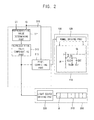
- FIG. 2 is a block diagram schematically illustrating the display apparatus of FIG. 1 , in accordance with an embodiment of the present invention.
- a display apparatus according to one embodiment includes a display unit 100, a backlight unit 200, and a controller board 300.
- the display unit 100 includes a display panel 110 and a panel driving part 120.
- the display panel 110 may include a first substrate 112, a second substrate 114 positioned opposite the first substrate 112, and a liquid crystal (LC) layer 116 interposed between the first substrate 112 and the second substrate 114.
- the first substrate 112 may include a plurality of pixels P displaying images.
- Each of the pixels P may include a switching element TR connected to a gate line GL and a data line DL, and a liquid crystal capacitor CLC and a storage capacitor CST that are connected to the switching element TR.
- the panel driving part 120 may include a source printed circuit board (PCB) 122, a data PCB 124 connecting the source PCB 122 and the display panel 110, and a gate driving circuit film 126 connected to the display panel 110.
- the data driving circuit film 124 is connected to data lines of the first substrate 126 and is connected to gate lines of the first substrate 112.
- the data driving circuit film 124 and the gate driving circuit film 126 may include a driving chip which outputs a driving signal for driving the display panel 110 in response to a control signal provided from the source PCB 122.
- the backlight unit 200 may include a light source 210, a light source driving part 220, a light guide plate 230, and a receiving container 240.
- the backlight unit 200 is disposed below the display unit 100 to provide the display unit 100 with light.
- the backlight unit 200 may be an edge type backlight unit disposed at a side of the light guide plate 230.
- the light source 210 may be a point light source, for example, a light-emitting diode (LED).
- the light source 210 is mounted on a driving substrate 214.
- the driving substrate 214 may include a plurality of control lines (not shown) for delivering a control signal and a plurality of power lines (not shown) for providing power to the light source 210.
- the light source 210 may include white LEDs emitting a white light.
- the light source 210 may include red LEDs emitting red light, green LEDs emitting green light, and/or blue LEDs emitting blue light.
- the light source 210 may include a plurality of unit light-emitting blocks B, and each unit light-emitting block B may include at least one LED.
- the unit light-emitting block B may be driven in a one-dimensional local dimming method in which the unit light-emitting block B is divided and driven with respect to one direction of a vertical direction or a horizontal direction.
- the unit light-emitting block B provides corresponding image blocks of the display panel 110 with light.
- the light source driving part 220 determines a duty cycle of the unit light-emitting block B by using a luminance compensation value of the unit light-emitting block B output from the controller board 300 and generates a plurality of driving signals based on the duty cycle.
- the light source driving part 220 provides the unit light-emitting block B with the driving signals to drive each of the unit light-emitting block B.
- the term “compensation” and/or “compensating” may be used the same meaning as “correction” and/or “correcting.”
- the light guide plate 230 is an optical plate which guides light exiting from the light source 210 to exit to an entire surface portion of the display panel 110.
- the light guide plate 230 may include a first surface F1, a second surface F2, a third surface F3, and a fourth surface F4.
- the first surface F1 is an incident portion of the light guide plate 230
- the third surface F3 is an exit portion of the light guide plate 230.
- the second surface F2 is a surface facing the first surface F1.
- the fourth surface F4 is parallel to the third surface F3, and is perpendicular to the first surface F1 and the second surface F2.
- the receiving container 240 may receive the display unit 100, the light source 210, the light guide plate 230, etc.
- the receiving container 240 includes a bottom portion and a plurality of side walls 244 extended from edges of the bottom portion 242.
- the backlight unit 200 may include optical sheets (not shown) disposed between the display panel 110 and the light guide plate 230 to enhance optical characteristics.
- the optical sheets may include a diffusion sheet enhancing the luminance uniformity of light and at least one prism sheets increasing a front luminance of light.
- the controller board 300 is electrically connected to the display unit 100 and the backlight unit 200 to control the display unit 100 and the backlight unit 200.
- the controller board 300 includes a controller unit 310, a first connector 340, a second connector 350, and a third connector 360.
- the first connector 340 is connected to an external device (not shown).
- the first connector 340 provides the controller unit 310 with an image signal IS and a control signal CS provided from the external device.
- the second connector 350 is electrically connected to the display unit 100 to provide the display unit 100 with the image signal IS.
- the third connector 360 is electrically connected to the light source driving part 220 of the backlight unit 200.
- the controller unit 310 includes a representative value determining part 311, a representative value compensating part 313, and a pixel correcting part 315.
- the representative value determining part 311 determines a luminance representative value of the unit light-emitting block B based on an external image signal provided to image blocks of the display panel 110 corresponding to the unit light-emitting block B.
- the representative value compensation part 313 compensates each of the luminance representative values to calculate a luminance compensation value.
- the luminance compensation value calculated from the representative value compensating part 313 is provided to the light source driving part 220 and the pixel correcting part 315.
- the pixel correcting part 315 applies a distance weight value to a boundary area of the unit light-emitting block B based on the luminance compensation value to correct pixel data of the image signal IS.
- the corrected pixel data is provided to the panel driving part 120.
- FIG. 3 is a block diagram illustrating a control unit of FIG. 2 , in accordance with an embodiment of the present invention.
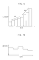
- FIGS. 4 , 5 , and 6 are diagrams illustrating a luminance compensation value that is compensated by a spatial compensation part 312 of FIG. 3 , in accordance with various embodiments of the present invention.
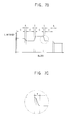
- FIG. 7A is a conceptual diagram explaining a luminance compensation value of a unit light-emitting block which is calculated from a representative value compensating part, in accordance with an embodiment of the present invention.
- FIG. 3 is a block diagram illustrating a control unit of FIG. 2 , in accordance with an embodiment of the present invention.
- FIGS. 4 , 5 , and 6 are diagrams illustrating a luminance compensation value that is compensated by a spatial compensation part 312 of FIG. 3 , in accordance with various embodiments of the present invention.
- FIG. 7A is a conceptual diagram explaining a luminance compensation value of a unit light-emitting block which is calculated
- FIG. 7B is a conceptual diagram explaining an estimated value of a luminance compensation value when a distance weight value is applied to a luminance compensation value by using a linear interpolation method at a boundary area of a unit light-emitting block, in accordance with an embodiment of the present invention.
- FIG. 7C is an enlarged plan view illustrating a boundary area 'A' of a unit light-emitting block 'B', in accordance with an embodiment of the present invention.
- FIG. 8A is an optical profile which models a luminance compensation value of FIG. 7A , in accordance with an embodiment of the present invention.
- FIG. 8B is an optical profile which models an estimated value of the luminance compensation value of FIG. 7B , in accordance with an embodiment of the present invention.
- the controller unit 310 includes a representative value determining part 311, a representative value compensating part 313, and a pixel correcting part 315.
- the representative value determining part 311 obtains a luminance representative value of the unit light-emitting block B by using the control signal CS and the image signal IS provided from an external device (not shown) corresponding to a plurality of image blocks divided in correspondence with the unit light-emitting block B.
- the luminance representative value may be an intermediate gradation value between a maximum gradation value and an average gradation value of image signal IS included in each image blocks.
- the representative value compensating part 323 may include a spatial compensation part 312 which low-pass filters a luminance representative value by the unit light-emitting block B.
- the spatial compensation part 312 may calculate a luminance compensation value of the unit light-emitting block B that is no less than a predetermined ratio with respect to the maximum luminance representative value of luminance representative values of the unit light-emitting block B adjacent to the unit light-emitting block B.
- FIG. 4A schematically shows a luminance representative value of the unit light-emitting block B determined at the representative value determining part 311
- FIG. 4B schematically shows a luminance compensation value of the unit light-emitting block B after the luminance representative value is low-pass filtered to be compensated.
- the determined luminance representative value When the determined luminance representative value is adapted to correct pixel data or drive the backlight unit 200, as shown in FIG. 4A , a dark block in which a luminance representative value is low between bright unit light-emitting blocks B may be generated. In this case, an image of the dark block may be darkly visible.
- the determined luminance representative value may be low-pass filtered, so that the brightness of the unit light-emitting block B may be controlled so as not to drop the determined luminance representative value to no more than a predetermined brightness in comparison with the brightness of the adjacent unit light-emitting block B.
- FIGS. 5 and 6 are diagrams illustrating compensation examples in which a luminance representative value of a unit light-emitting block B is spatially low-pass filtered.
- a luminance representative value of each unit light-emitting block B has a value that is less than a first compensation ratio in comparison with a high value of a luminance representative value of adjacent unit light-emitting blocks B
- each unit light-emitting block is compensated to have no less than the first compensation value of the maximum luminance representative value so that a luminance compensation value may be calculated.
- the luminance of a unit light-emitting block B may be decreased without rapid variation of a luminance representative value of adjacent unit light-emitting blocks B with respect to a unit light-emitting block B having the highest brightness that is positioned at a right side of FIG. 5 .
- the first compensation ratio may be about 80%.
- the luminance representative value of the unit light-emitting block B may be spatially low-pass filtered to have the different compensating amount in regard to an average brightness of the adjacent unit light-emitting block B.
- the brightness of the unit light-emitting blocks B having a relatively bright luminance is set to have a high compensation ratio so that power consumption may be decreased
- the brightness of the unit light-emitting blocks B having a relatively dark luminance is set to have a low compensation ratio so that disadvantages where a dark object is not visible may be solved.
- luminance representative values of bright unit light-emitting blocks B are gradually decreased by a first compensation ratio and a luminance representative value of dark unit light-emitting blocks B are gradually decreased by a second compensation ratio.
- the first compensation ratio may be about 80%
- the second compensation ratio may be about 95%.
- the luminance representative values of the unit light-emitting blocks B that are classified by an average brightness may be compensated in compensation ratios different from each other.
- the compensation ratios may be more than two.
- the representative value compensating part 313 may include a temporal compensation part 314 which low-pass filters a luminance representative value of the unit light-emitting block B by each frame of the image signal IS.
- the temporal compensation part 314 may compensate a luminance representative value of n-th unit light-emitting block B per each frame of an image signal IS by using the following Equation 1.
- Lk' denotes a luminance representative value of an k-th frame after compensating
- Lk denotes a luminance representative value of the k-th frame
- L'k-1 denotes a luminance representative value of a (k-1)-th frame after compensating
- PARA denotes a low-pass filtering level
- AVEk denotes an average gradation value of an external image signal of the k-th frame
- AVEk-1 denotes an average gradation value of the external image signal of the (k-1)-th frame.
- the representative value compensating part 313 may include a spatial compensation part 312 and a temporal compensation part 314.
- the spatial compensation part 312 may low-pass filter a luminance representative value by the unit light-emitting block B at a space axis.
- the temporal compensation part 314 may low-pass filter a luminance representative value of the unit light-emitting block B at a time axis.
- an employing sequence of the spatial compensation part 312 and the temporal compensation part 314 may be various. As shown in FIG.
- Lk', Lk and L'k-1 of Equation 1 that is applied to the temporal compensation part 314 may represent a luminance compensation value that is calculated by the spatial compensation part 312 and not a luminance representative value of the unit light-emitting block B.
- the representative value compensating part 313 calculates a luminance compensation value that each of the luminance representative value is compensated, and provides the light source driving part 220 and the pixel correcting part 315 with the luminance compensation value.
- the light source driving part 220 determines a duty cycle of the unit light-emitting block B with respect to the luminance compensation value.
- the light source driving part 220 generates a plurality of driving signals based on the duty cycle, and drives each of the unit light-emitting blocks B.
- the pixel correcting part 315 compensates pixel data to enhance a luminance of an image so as to compensate that a whole screen is darker due to a dimming of a backlight.
- the pixel correcting part 315 applies a distance weight value to a boundary area of the unit light-emitting block B, based on the luminance compensation value provided from the representative value compensating part 313, to compensate pixel data of the image signal.
- the pixel correcting part 315 may correct each pixel by setting a predetermined area between the unit light-emitting blocks B as a boundary area and setting the remaining area of the boundary area as a center area. Pixels corresponding to the center area may be corrected based on the luminance compensation value provided from the representative value compensation part 313. On the other hand, pixels corresponding to the boundary area may be corrected based on an estimated value by adding a distance weight value to a luminance compensation value, so that rapid luminance differences between unit light-emitting blocks B may be decreased.
- FIG. 7A is a conceptual diagram explaining a luminance compensation value of a unit light-emitting block which is calculated from a representative value compensating part, in accordance with an embodiment of the present invention.
- FIG. 7B is a conceptual diagram explaining an estimated value of a luminance compensation value when a distance weight value is applied to a luminance compensation value by using a linear interpolation method at a boundary area of a unit light-emitting block B, in accordance with an embodiment of the present invention.
- FIG. 7C is an enlarged plan view illustrating a boundary area 'A' of a unit light-emitting block 'B', in accordance with an embodiment of the present invention.
- the pixel correcting part 315 includes a boundary area luminance calculating part 316 and pixel data correcting part 318.
- the pixel compensating part 315 may include a point spread function (PSF) part (not shown).
- PSF point spread function
- the PSF part corrects a luminance compensation value calculated at the representative value compensating part 313 in reference to luminance interference of a peripheral unit light-emitting blocks B which influences a luminance of the unit light-emitting block B.
- the pixel data may be applied to the pixel of the display panel through the boundary area luminance calculating part 316 and the pixel data correcting part 318 based on the luminance correction value that is compensated at the PSF part.
- the boundary area luminance calculating part 316 may apply a luminance compensation value or a luminance compensation value corrected by the PSF part calculate by using a linear interpolation method.
- estimated values of a luminance compensation value or estimated values of the corrected luminance compensation value may be calculated in the boundary area A of the unit light-emitting block B.
- the pixel data correcting part 318 may calculate pixel data of a center area C and a boundary area A of the unit light-emitting block B, based on an estimated value of the corrected unit light-emitting block B by the PSF part and estimated values of the luminance compensation value at a boundary area A that are calculated by a linear interpolation method by the boundary area luminance calculating part 316.
- the boundary area luminance calculating part 316 gradually decreases a difference of the luminance compensation value at a boundary area A of the unit light-emitting block B, so that disadvantages where a boundary area between unit light-emitting blocks B is visible, which is generated due to rapid luminance differences in the boundary area A of the unit light-emitting block B, may be solved.
- FIG. 8A is an optical profile that models a luminance compensation value of FIG. 7A , in accordance with an embodiment of the present invention.
- FIG. 8B is an optical profile which models an estimated value of the luminance compensation value of FIG. 7B , in accordance with an embodiment of the present invention.
- the pixel data correcting part 318 corrects pixel data of the image signal IS based on the corrected luminance compensation value of the unit light-emitting block B and estimated values of the luminance compensation value at the boundary area A that are calculated by the boundary area luminance calculating part 316.
- the correction of the pixel data uses a slope value based on a gamma equation, and thus a calculation may be omitted. Therefore, hardware size may be decreased.
- the pixel data of the image signal IS may be corrected by multiplying a correction coefficient in accordance with a dimming of the backlight unit 200 based on gamma characteristics of the display panel 110.
- the correction coefficient ' ⁇ ' may be defined by the following Equation 2.
- G' denotes pixel data of an image signal IS after the pixel data of the image signal is compensated
- G denotes pixel data of the image signal IS
- Gmax denotes a maximum gradation value of the pixel data
- Grep denotes a compensated luminance compensation value at a center area C of the unit light-emitting block B or an estimated value of a luminance compensation value at a boundary area A of the unit light-emitting block B
- DR denotes a dimming ratio.
- pixel data of the image signal IS may be corrected by multiplying a compensating coefficient ' ⁇ '.
- FIG. 9 is a flowchart showing a method of driving a display apparatus, in accordance with an exemplary embodiment of the present invention.
- the representative value determining part 311 determines a luminance representative value of the unit light-emitting block B from an external image signal IS corresponding to a plurality of image blocks corresponding to the unit light-emitting block B (step S 100).
- the representative value compensating part 313 compensates each of the luminance representative values to calculate a luminance compensation value of the unit light-emitting block B (step S300).
- the pixel correcting part 315 corrects pixel data of the image signal IS at a center area C and a boundary area A of the unit light-emitting block B based on the luminance compensation value (step S500).
- step S500 a step of calculating the corrected luminance compensation value that is corrected by the PSF part may be further performed.
- the PSF part corrects a luminance compensation value in regard to luminance interference of adjacent unit light-emitting blocks B based on the luminance compensation value.
- the pixel correcting part 315 may correct pixel data of the image signal IS at the center area C and the boundary area A of the unit light-emitting block B, based on the corrected luminance compensation value.
- the light source driving part 220 determines a duty cycle of the unit light-emitting block B based on the luminance compensation value, generates a plurality of driving signals based on the duty cycle, and provides the unit light-emitting block B with the driving signals to drive each of the unit light-emitting blocks B (step S700).
- the display unit 100 displays an image based on the corrected pixel data, and the backlight unit 200 generates a driving signal based on the luminance compensation value to provide the unit light-emitting block B with the driving signal.
- the representative value determining part 311 obtains a maximum gradation value and an average gradation value of luminance of the unit light-emitting block 311 by using the control signal CS and the image signal IS that are provided from an external device (not shown).
- the control signal CS and the image signal IS may correspond to a plurality of image blocks that is divided into in correspondence with the unit light-emitting block B.
- the representative value determining part 311 may determine a predetermined value between the maximum gradation value and the average gradation value of the unit light-emitting block B as a luminance representative value of the unit light-emitting block B.
- the spatial compensation part 312 may low-pass filter a luminance representative value per the unit light-emitting block B.
- the spatial compensation part 312 may calculate a luminance compensation value of the unit light-emitting block B that is no less than a predetermined ratio with respect to the maximum luminance representative value of luminance representative values of the unit light-emitting block B adjacent to the unit light-emitting block B.
- the determined luminance representative value may be low-pass filtered, so that the brightness of the unit light-emitting block B may be controlled so as not to drop the determined luminance representative value to no more than a predetermined brightness in comparison with the brightness of the adjacent unit light-emitting block B.
- each unit light-emitting block B when a luminance representative value of each unit light-emitting block B has a value that is less than a first compensation ratio in comparison with a high value of a luminance representative value of adjacent unit light-emitting blocks B, each unit light-emitting block is corrected to have no less than the first compensation value of the maximum luminance representative value so that a luminance compensation value may be calculated.
- the luminance of the unit light-emitting block B may be decreased without rapid variation of a luminance representative value of adjacent unit light-emitting blocks B with respect to a unit light-emitting block B having the highest brightness that is positioned at a right side of FIG. 5 .
- the first compensation ratio may be about 80%.
- the luminance representative value of the unit light-emitting block B may be spatially low-pass filtered to have the different compensating amount in regard to an average brightness of the adjacent unit light-emitting block B.
- the brightness of the unit light-emitting blocks B having a relatively bright luminance is set to have a high compensation ratio so that power consumption may be decreased
- the brightness of the unit light-emitting blocks B having a relatively dark luminance is set to have a low compensation ratio so that disadvantages where a dark object is not visible may be solved.
- luminance representative values of bright unit light-emitting blocks B are gradually decreased by a first compensation ratio and a luminance representative value of dark unit light-emitting blocks B are gradually decreased by a second compensation ratio.
- the first compensation ratio may be about 80%
- the second compensation ratio may be about 95%.
- the luminance representative values of the unit light-emitting blocks B that are classified by an average brightness may be compensated in compensation ratios different from each other.
- the compensation ratios may be more than two.
- the temporal compensation part 314 may low-pass filter the luminance representative value of the unit light-emitting block B by each frame of the image signal IS.
- the temporal compensation part 314 may low-pass filter a luminance representative value of the unit light-emitting block B at a time axis, so that brightness variation of blocks between frames may be controlled.
- the temporal compensation part 314 may compensate the luminance representative value of the n-th unit light-emitting block B by each frame of the image signal IS by using Equation 1. According to Equation 1, the brightness of the unit light-emitting block B may be compensated by using a brightness difference between a previous frame and a current frame.
- step S500 in order to compensate that a full screen is dark due to a dimming driving of the backlight unit 200, the pixel correcting part 315 corrects pixel data to increase luminance of an image.
- the pixel correcting part 315 corrects pixel data of the image signal IS by applying a distance weight value to a boundary are of the unit light-emitting block B based on a luminance compensation value provided from the representative value compensating part 313.
- the pixel correcting part 315 may correct each pixel by setting a predetermined area between the unit light-emitting blocks B as a boundary area and setting the remaining area of the boundary area as a center area. Pixels corresponding to the center area may be corrected based on the luminance compensation value. On the other hand, pixels corresponding to the boundary area may be corrected based on an estimated value by adding a distance weight value to a luminance compensation value, so that rapid luminance differences between unit light-emitting blocks B may be decreased.
- the pixel correcting part 315 includes a boundary area luminance calculating part 316 and pixel data correcting part 318.
- the pixel compensating part 315 may further include a point spread function (PSF) part (not shown).
- PSF point spread function
- the PSF part corrects a luminance compensation value calculated at the representative value compensating part 313 in regard to luminance interference of a peripheral unit light-emitting blocks B which influences a luminance of the unit light-emitting block B.
- the pixel data may be applied to the pixel of the display panel through the boundary area luminance calculating part 316 and the pixel data correcting part 318 based on the luminance correction value that is corrected at the PSF part.
- the boundary area luminance calculating part 316 When the boundary area luminance calculating part 316 obtains pixel data of a pixel corresponding to the boundary area A of the unit light-emitting block B, the boundary area luminance calculating part 316 applies a distance weight value to the luminance compensation value or the corrected luminance compensation value that is corrected by the PSF part to calculate an estimated value of the luminance compensation value corresponding to the boundary area A.
- the boundary area luminance calculating part 316 may apply a luminance compensation value or a luminance compensation value corrected by the PSF part calculate by using a linear interpolation method.
- estimated values of a luminance compensation value or estimated values of the corrected luminance compensation value may be calculated in the boundary area A of the unit light-emitting block B.
- the pixel data correcting part 318 may calculate pixel data of a center area C and a boundary area A of the unit light-emitting block B, based on an estimated value of the corrected unit light-emitting block B by the PSF part and estimated values of the luminance compensation value at a boundary area A that are calculated in a linear interpolation method by the boundary area luminance calculating part 316.
- the boundary area luminance calculating part 316 gradually decreases a difference of the luminance compensation value at a boundary area A of the unit light-emitting block B, so that disadvantages in that a boundary area between unit light-emitting blocks B is visible, which is generated due to rapid luminance differences in the boundary area A of the unit light-emitting block B, may be solved.
- the pixel data correcting part 318 corrects pixel data of the image signal IS based on the corrected luminance compensation value of the unit light-emitting block B and estimated values of the luminance compensation value at the boundary area A that are calculated by the boundary area luminance calculating part 316.
- the correction of the pixel data uses a slope value based on a gamma equation, and thus a calculation may be omitted. Therefore, hardware size may be decreased.
- the pixel data of the image signal IS may be corrected by multiplying a correction coefficient in accordance with a dimming of the backlight unit 200 based on gamma characteristics of the display panel 110.
- the correction coefficient ' ⁇ ' of the pixel data may be defined by Equation 2. In one aspect, referring to Equation 2, pixel data of the image signal IS may be corrected by multiplying a correction coefficient.
- a luminance representative value of the unit light-emitting block B is compensated in temporal and spatial and then the pixel data is corrected, so that flicker generated between unit light-emitting blocks B and between frames of an image signal may be removed.
- difference of luminance compensation values at the boundary area A of the unit light-emitting block B may be decreased to correct pixel data of the image signal IS, so that the visibility of a boundary of the unit light-emitting block B may be decreased so that display quality may be enhanced.
- the method of driving a display apparatus according to the present invention is applied to a display apparatus having a backlight unit such as an LED.
- a display apparatus applying the method of driving a display apparatus according to the present invention will be described.
- FIG. 10 is a perspective view illustrating a display apparatus, in accordance with another exemplary embodiment of the present invention.
- a display apparatus according to another exemplary embodiment of the present invention includes a display unit 100, a backlight unit 400 and a controller board 300.
- the display apparatus according to another exemplary embodiment of the present invention is substantially the same as the display apparatus of FIG. 1 except for at least the backlight unit 400.
- identical reference numerals are used in FIG. 10 to refer to components are the same or like those shown in FIG. 1 , and thus, a detailed description thereof will be omitted.
- the backlight unit 400 may include a plurality of lamps 410, a light source driving part 220 and a receiving container 430.
- the backlight unit 400 is disposed below the display unit 100 to provide the display unit 100 with light.
- the light source driving part 220 according to the present embodiment of the present invention is substantially the same as the light source driving part 220 of FIG. 2 .
- the same reference numerals will be used to refer to the same or like parts as those described in this embodiment and any further explanation concerning the above elements will be omitted.
- the lamps 410 are disposed on the receiving container 430 to be driven in a vertical direction crossing a length direction of the lamps 410. That is, the lamps 410 may employ a first dimension dimming method in which the lamps 410 are classified into a predetermined number with respect to the vertical direction to be driven.
- the lamps may be sequentially driven in the vertical direction by a unit of one lamp.
- one lamp may define a unit light-emitting block B.
- the lamps may be sequentially driven in the vertical direction by a unit of two or more than two lamps.
- the two or more than two lamps may define a unit light-emitting block B.
- a plurality of supporting members 440 respectively supporting two end portions of the lamps may be further disposed on the backlight unit 400.
- One supporting member 442 may support a first end portion of the lamp, and the another supporting member 444 may support a second end portion of the lamp.
- the receiving container 430 may receive the display unit 100 and the lamps 410.
- the backlight unit 400 may further include a reflection sheet 450 disposed between the lamps 410 and the receiving container 430 to reflect light emitted from the lamps 410 to the display unit 100.
- the backlight unit 400 may further include optical sheets 460 disposed on the lamps 410 to enhance optical characteristics.
- the optical sheets 460 may include a diffusion sheet 462 enhancing the luminance uniformity of light and at least one prism sheet 464 enhancing a front luminance of light.
- the backlight unit may be driven by using a local dimming driving method, so that power consumption thereof may be decreased.
- the pixel data may be corrected by applying a weight value in accordance with a distance at a boundary area of the unit light-emitting block, so that the display quality of the display apparatus may be enhanced.
Landscapes
- Physics & Mathematics (AREA)
- Engineering & Computer Science (AREA)
- General Physics & Mathematics (AREA)
- Computer Hardware Design (AREA)
- Theoretical Computer Science (AREA)
- Chemical & Material Sciences (AREA)
- Crystallography & Structural Chemistry (AREA)
- Nonlinear Science (AREA)
- Mathematical Physics (AREA)
- Optics & Photonics (AREA)
- Control Of Indicators Other Than Cathode Ray Tubes (AREA)
- Liquid Crystal Display Device Control (AREA)
- Liquid Crystal (AREA)
Applications Claiming Priority (2)
| Application Number | Priority Date | Filing Date | Title |
|---|---|---|---|
| KR1020090024794A KR101605157B1 (ko) | 2009-03-24 | 2009-03-24 | 표시 장치 구동 방법 |
| EP09013927A EP2234096A3 (de) | 2009-03-24 | 2009-11-06 | Ansteuerverfahren für eine Anzeigevorrichtung |
Related Parent Applications (1)
| Application Number | Title | Priority Date | Filing Date |
|---|---|---|---|
| EP09013927A Division EP2234096A3 (de) | 2009-03-24 | 2009-11-06 | Ansteuerverfahren für eine Anzeigevorrichtung |
Publications (2)
| Publication Number | Publication Date |
|---|---|
| EP2772901A2 true EP2772901A2 (de) | 2014-09-03 |
| EP2772901A3 EP2772901A3 (de) | 2015-12-09 |
Family
ID=42320175
Family Applications (2)
| Application Number | Title | Priority Date | Filing Date |
|---|---|---|---|
| EP14167620.5A Ceased EP2772901A3 (de) | 2009-03-24 | 2009-11-06 | Verfahren zur Ansteuerung einer Anzeigevorrichtung |
| EP09013927A Withdrawn EP2234096A3 (de) | 2009-03-24 | 2009-11-06 | Ansteuerverfahren für eine Anzeigevorrichtung |
Family Applications After (1)
| Application Number | Title | Priority Date | Filing Date |
|---|---|---|---|
| EP09013927A Withdrawn EP2234096A3 (de) | 2009-03-24 | 2009-11-06 | Ansteuerverfahren für eine Anzeigevorrichtung |
Country Status (5)
| Country | Link |
|---|---|
| US (1) | US8482509B2 (de) |
| EP (2) | EP2772901A3 (de) |
| JP (1) | JP5570791B2 (de) |
| KR (1) | KR101605157B1 (de) |
| CN (1) | CN101847369B (de) |
Cited By (2)
| Publication number | Priority date | Publication date | Assignee | Title |
|---|---|---|---|---|
| CN105023539A (zh) * | 2015-07-10 | 2015-11-04 | 北京大学深圳研究生院 | 一种像素矩阵的外围补偿系统、方法和显示系统 |
| CN109979401A (zh) * | 2019-05-06 | 2019-07-05 | 京东方科技集团股份有限公司 | 驱动方法、驱动装置、显示设备和计算机可读介质 |
Families Citing this family (46)
| Publication number | Priority date | Publication date | Assignee | Title |
|---|---|---|---|---|
| KR101571732B1 (ko) | 2009-06-26 | 2015-11-25 | 엘지전자 주식회사 | 액정표시장치 및 그 구동방법 |
| KR101580921B1 (ko) * | 2009-08-14 | 2015-12-30 | 삼성디스플레이 주식회사 | 표시 장치 |
| CN102110403B (zh) * | 2009-12-23 | 2013-04-17 | 群康科技(深圳)有限公司 | 改善显示器拖影现象的方法及相关的显示器 |
| KR20110131543A (ko) * | 2010-05-31 | 2011-12-07 | 삼성엘이디 주식회사 | 백라이트 유닛 |
| TWI408444B (zh) * | 2010-09-30 | 2013-09-11 | Au Optronics Corp | 液晶顯示器及其訊號傳輸裝置 |
| KR101908686B1 (ko) | 2011-11-07 | 2018-10-17 | 삼성디스플레이 주식회사 | 표시 장치 및 그 구동 방법 |
| JP2013246261A (ja) * | 2012-05-24 | 2013-12-09 | Sharp Corp | 表示装置及び表示装置の駆動方法 |
| JP6202786B2 (ja) * | 2012-05-30 | 2017-09-27 | キヤノン株式会社 | 表示制御装置、表示制御装置の制御方法 |
| KR102005760B1 (ko) * | 2012-11-27 | 2019-08-02 | 엘지디스플레이 주식회사 | 타이밍 컨트롤러 및 그 구동 방법과 이를 이용한 표시장치 |
| JP6182914B2 (ja) * | 2013-03-13 | 2017-08-23 | セイコーエプソン株式会社 | 電気光学装置及び電子機器 |
| KR101461995B1 (ko) * | 2013-05-14 | 2014-11-24 | (주)코텍 | 평면 디스플레이 패널의 휘도 균일성 보상 장치 및 그 방법 |
| CN103474016B (zh) * | 2013-09-11 | 2016-06-22 | 青岛海信电器股份有限公司 | 分区驱动处理方法、处理装置及显示器 |
| KR102151262B1 (ko) * | 2013-09-11 | 2020-09-03 | 삼성디스플레이 주식회사 | 표시 패널의 구동 방법, 이를 수행하는 표시 장치, 이에 적용되는 보정값 산출 방법 및 계조 데이터의 보정 방법 |
| KR102169870B1 (ko) * | 2013-12-23 | 2020-10-27 | 삼성디스플레이 주식회사 | 영상 처리 컨트롤러, 표시 장치 및 그것의 구동 방법 |
| JP6347957B2 (ja) * | 2014-01-17 | 2018-06-27 | シナプティクス・ジャパン合同会社 | 表示装置、表示パネルドライバ、及び、表示パネルの駆動方法 |
| CN104021774B (zh) * | 2014-05-29 | 2016-06-15 | 京东方科技集团股份有限公司 | 一种图像处理的方法及装置 |
| LU92598B1 (en) * | 2014-11-17 | 2016-05-18 | Universität des Saarlandes | A local dimming algorithm and device |
| KR102366198B1 (ko) * | 2014-12-08 | 2022-02-23 | 엘지디스플레이 주식회사 | 표시장치 및 그의 구동방법 |
| KR102320768B1 (ko) * | 2015-05-12 | 2021-11-02 | 삼성디스플레이 주식회사 | 터치 패널 및 그 보정 방법 |
| CN105185328B (zh) | 2015-09-01 | 2018-01-09 | 青岛海信电器股份有限公司 | 液晶显示亮度控制方法和装置以及液晶显示设备 |
| CN105139809B (zh) * | 2015-09-01 | 2018-06-12 | 青岛海信电器股份有限公司 | 液晶显示亮度控制方法和装置以及液晶显示设备 |
| CN105047142B (zh) | 2015-09-01 | 2017-11-24 | 青岛海信电器股份有限公司 | 液晶显示亮度控制方法和装置以及液晶显示设备 |
| CN105185327B (zh) | 2015-09-01 | 2018-02-06 | 青岛海信电器股份有限公司 | 液晶显示亮度控制方法和装置以及液晶显示设备 |
| CN105161064B (zh) | 2015-09-17 | 2018-06-26 | 青岛海信电器股份有限公司 | 液晶显示亮度控制方法和装置以及液晶显示设备 |
| CN105118474B (zh) | 2015-10-16 | 2017-11-07 | 青岛海信电器股份有限公司 | 液晶显示亮度控制方法和装置以及液晶显示设备 |
| CN105185353B (zh) | 2015-10-16 | 2018-05-18 | 青岛海信电器股份有限公司 | 液晶显示亮度控制方法和装置以及液晶显示设备 |
| JP6629055B2 (ja) * | 2015-11-30 | 2020-01-15 | 株式会社ソニー・インタラクティブエンタテインメント | 情報処理装置および情報処理方法 |
| JP7044478B2 (ja) * | 2016-05-09 | 2022-03-30 | 株式会社ジャパンディスプレイ | 表示装置 |
| CN106023905B (zh) | 2016-05-27 | 2019-05-10 | 京东方科技集团股份有限公司 | 控制显示设备的方法、显示设备的控制装置以及显示设备 |
| KR102702307B1 (ko) | 2016-08-03 | 2024-09-04 | 삼성전자주식회사 | 디스플레이 장치 및 전자 장치의 제어 방법 |
| WO2018083928A1 (ja) * | 2016-11-07 | 2018-05-11 | シャープ株式会社 | 画像表示装置および画像表示方法 |
| KR20180058266A (ko) | 2016-11-23 | 2018-06-01 | 삼성디스플레이 주식회사 | 표시 장치 및 이의 휘도 보상 방법 |
| KR102581190B1 (ko) * | 2016-12-14 | 2023-09-21 | 삼성전자주식회사 | 디스플레이 장치 및 심 조정 방법 |
| KR102746145B1 (ko) * | 2016-12-21 | 2024-12-27 | 삼성디스플레이 주식회사 | 표시장치 및 그의 구동방법 |
| US10770008B2 (en) * | 2017-07-31 | 2020-09-08 | Japan Display Inc. | Display device with dimming panel |
| CN108665866B (zh) | 2018-05-18 | 2021-03-16 | 京东方科技集团股份有限公司 | 获取背光源扩散传输参数的方法及显示控制方法和装置 |
| WO2020112085A1 (en) | 2018-11-27 | 2020-06-04 | Hewlett-Packard Development Company, L.P. | Displays with dimming zones that change |
| KR102646911B1 (ko) | 2019-03-14 | 2024-03-14 | 삼성디스플레이 주식회사 | 표시 장치 |
| KR102686100B1 (ko) * | 2019-07-18 | 2024-07-19 | 삼성디스플레이 주식회사 | 표시 패널의 구동 방법 및 이를 수행하기 위한 표시 장치 |
| TWI721808B (zh) * | 2020-03-04 | 2021-03-11 | 和碩聯合科技股份有限公司 | 亮度補償方法 |
| CN114464143B (zh) * | 2020-11-10 | 2023-07-18 | 上海天马微电子有限公司 | 控制显示装置的背光源的方法及显示装置 |
| US11804187B2 (en) | 2021-06-25 | 2023-10-31 | Apple Inc. | Displays with reduced color non-uniformity |
| CN114550672B (zh) * | 2022-03-30 | 2023-05-30 | Tcl华星光电技术有限公司 | 显示面板亮度的补偿方法、其设备及存储介质 |
| CN119173939A (zh) * | 2022-05-12 | 2024-12-20 | 惠普发展公司,有限责任合伙企业 | 发光二极管驱动器的功率水平 |
| CN115881020B (zh) * | 2023-01-18 | 2025-05-02 | 合肥维信诺科技有限公司 | 显示面板校正方法、装置、显示装置制备方法及存储介质 |
| CN119032392B (zh) * | 2023-03-24 | 2026-01-13 | 京东方科技集团股份有限公司 | 背光扩散参数生成方法、显示控制方法及装置、显示装置 |
Family Cites Families (28)
| Publication number | Priority date | Publication date | Assignee | Title |
|---|---|---|---|---|
| US5974174A (en) * | 1996-09-26 | 1999-10-26 | Victor Company Of Japan, Ltd. | Picture-information processing apparatus |
| US6608617B2 (en) | 2000-05-09 | 2003-08-19 | Marc O. Hoffknecht | Lighting control interface |
| JP4628770B2 (ja) * | 2004-02-09 | 2011-02-09 | 株式会社日立製作所 | 照明装置を備えた画像表示装置及び画像表示方法 |
| KR20050112905A (ko) | 2004-05-28 | 2005-12-01 | 엘지.필립스 엘시디 주식회사 | 백라이트 유닛의 휘도 제어방법 |
| US7525528B2 (en) * | 2004-11-16 | 2009-04-28 | Sharp Laboratories Of America, Inc. | Technique that preserves specular highlights |
| KR100727648B1 (ko) | 2005-06-03 | 2007-06-13 | 광주과학기술원 | Lcd 백라이트 유닛을 형성하는 휘도의 균일성을 높이는복층구조의 도광판 |
| JP4951973B2 (ja) * | 2006-01-10 | 2012-06-13 | ソニー株式会社 | 表示装置及び表示方法 |
| JP5338019B2 (ja) | 2006-02-10 | 2013-11-13 | セイコーエプソン株式会社 | 画像表示装置 |
| JP4810249B2 (ja) * | 2006-02-15 | 2011-11-09 | Necディスプレイソリューションズ株式会社 | 映像表示装置および輝度較差補正方法 |
| KR100790698B1 (ko) * | 2006-04-19 | 2008-01-02 | 삼성전기주식회사 | 액정표시장치용 백라이트 유닛 |
| KR100780205B1 (ko) | 2006-04-21 | 2007-11-27 | 삼성전기주식회사 | 액정표시장치용 백라이트 유닛 |
| TWI328133B (en) * | 2006-05-12 | 2010-08-01 | Au Optronics Corp | Method for eliminating the shadow around support pin of led backlight |
| KR100831369B1 (ko) * | 2006-06-09 | 2008-05-21 | 삼성전자주식회사 | 표시장치용 백라이트장치 및 그 밝기조절방법 |
| US20070285379A1 (en) * | 2006-06-09 | 2007-12-13 | Samsung Electronics Co., Ltd. | Liquid crystal display and method of adjusting brightness for the same |
| JP4208909B2 (ja) * | 2006-08-24 | 2009-01-14 | 株式会社東芝 | 画像処理装置と撮影装置 |
| JP2008125049A (ja) * | 2006-10-20 | 2008-05-29 | Rohm Co Ltd | 画像処理ic、画像処理装置、バックライト駆動装置 |
| JP4237220B2 (ja) * | 2006-11-13 | 2009-03-11 | シャープ株式会社 | 透過型ディスプレイ装置 |
| KR101351887B1 (ko) | 2006-11-21 | 2014-01-17 | 엘지디스플레이 주식회사 | 액정표시장치 |
| KR20080058518A (ko) | 2006-12-22 | 2008-06-26 | 삼성전자주식회사 | 백라이트 어셈블리 및 이를 갖는 액정표시장치 |
| KR20080068947A (ko) | 2007-01-22 | 2008-07-25 | 삼성코닝정밀유리 주식회사 | 셀전극을 구비하는 면광원 장치 및 이를 포함하는 백라이트유닛 |
| KR101410465B1 (ko) | 2007-02-22 | 2014-06-23 | 삼성디스플레이 주식회사 | 백라이트 장치 및 이를 갖는 액정표시장치 |
| KR100828104B1 (ko) | 2007-03-27 | 2008-05-08 | 금호전기주식회사 | 전계 방출형 램프 |
| KR101333680B1 (ko) * | 2007-04-12 | 2013-12-02 | 삼성전자주식회사 | 디스플레이장치 및 그의 밝기 조정방법 |
| JP2008268717A (ja) * | 2007-04-24 | 2008-11-06 | Renesas Technology Corp | 画像表示装置の駆動回路および画像表示方法 |
| KR100944595B1 (ko) * | 2007-04-24 | 2010-02-25 | 가부시끼가이샤 르네사스 테크놀로지 | 표시 장치, 표시 장치 구동 회로, 화상 표시 방법, 전자기기 및 화상 표시 장치 구동 회로 |
| KR100885285B1 (ko) * | 2007-05-08 | 2009-02-23 | 닛뽕빅터 가부시키가이샤 | 액정 표시 장치 및 이에 이용되는 영상 표시 방법 |
| US7855725B2 (en) * | 2007-09-26 | 2010-12-21 | Himax Technologies Limited | Method of controlling backlight module, backlight controller and display device using the same |
| KR100868531B1 (ko) | 2007-12-17 | 2008-11-13 | 한국전자통신연구원 | 미세 로컬 디밍이 가능한 전계 방출 장치 |
-
2009
- 2009-03-24 KR KR1020090024794A patent/KR101605157B1/ko not_active Expired - Fee Related
- 2009-10-29 US US12/608,763 patent/US8482509B2/en not_active Expired - Fee Related
- 2009-11-06 EP EP14167620.5A patent/EP2772901A3/de not_active Ceased
- 2009-11-06 EP EP09013927A patent/EP2234096A3/de not_active Withdrawn
- 2009-12-03 JP JP2009275394A patent/JP5570791B2/ja not_active Expired - Fee Related
- 2009-12-24 CN CN200910261385.6A patent/CN101847369B/zh not_active Expired - Fee Related
Non-Patent Citations (1)
| Title |
|---|
| None |
Cited By (4)
| Publication number | Priority date | Publication date | Assignee | Title |
|---|---|---|---|---|
| CN105023539A (zh) * | 2015-07-10 | 2015-11-04 | 北京大学深圳研究生院 | 一种像素矩阵的外围补偿系统、方法和显示系统 |
| CN105023539B (zh) * | 2015-07-10 | 2017-11-28 | 北京大学深圳研究生院 | 一种像素矩阵的外围补偿系统、方法和显示系统 |
| CN109979401A (zh) * | 2019-05-06 | 2019-07-05 | 京东方科技集团股份有限公司 | 驱动方法、驱动装置、显示设备和计算机可读介质 |
| CN109979401B (zh) * | 2019-05-06 | 2021-01-08 | 京东方科技集团股份有限公司 | 驱动方法、驱动装置、显示设备和计算机可读介质 |
Also Published As
| Publication number | Publication date |
|---|---|
| CN101847369A (zh) | 2010-09-29 |
| EP2772901A3 (de) | 2015-12-09 |
| JP2010224516A (ja) | 2010-10-07 |
| KR101605157B1 (ko) | 2016-03-22 |
| US20100245397A1 (en) | 2010-09-30 |
| EP2234096A2 (de) | 2010-09-29 |
| KR20100106703A (ko) | 2010-10-04 |
| EP2234096A3 (de) | 2011-06-15 |
| US8482509B2 (en) | 2013-07-09 |
| JP5570791B2 (ja) | 2014-08-13 |
| CN101847369B (zh) | 2014-08-20 |
Similar Documents
| Publication | Publication Date | Title |
|---|---|---|
| US8482509B2 (en) | Method of driving a display apparatus to compensate for uneven backlighting | |
| US8599126B2 (en) | Method of local dimming of light source, light source apparatus for performing the method and display apparatus having the light source apparatus | |
| EP2148318B1 (de) | Verfahren zur Verstärkung eines Anzeigebildes, Steuerungseinheit zur Durchführung des Verfahrens und Anzeigevorrichtung mit der Steuerungseinheit | |
| US8797366B2 (en) | Method of driving a light source, light source apparatus for performing the method and display apparatus having the light source apparatus | |
| US9035868B2 (en) | Method for driving a light source module and display apparatus for performing the method | |
| CN102097071B (zh) | 液晶显示设备的局部调光驱动方法和设备 | |
| US8760385B2 (en) | Liquid crystal display device and method for local dimming driving using spatial filter of the same | |
| US8830158B2 (en) | Method of local dimming a light source, light source apparatus for performing the method, and display apparatus having the light source apparatus | |
| EP2221796B1 (de) | Verfahren zur Steuerung einer Lichtquelle, Hintergrundbeleuchtungsvorrichtung zur Durchführung des Verfahrens und Flüssigkristallanzeigevorrichtung mit der Hintergrundbeleuchtungsvorrichtung | |
| US8638339B2 (en) | Method for correcting pixel data, and display apparatus for performing the method | |
| US9041745B2 (en) | Method of boosting a local dimming signal, boosting drive circuit for performing the method, and display apparatus having the boosting drive circuit | |
| US8766903B2 (en) | Method of driving a light source, light source apparatus for performing the method and display apparatus having the light source apparatus | |
| KR20060087908A (ko) | 귀환 회로부가 구비되는 액정표시장치 | |
| KR101588340B1 (ko) | 표시 장치 및 그 구동 방법 | |
| KR101213898B1 (ko) | 액정표시장치의 백라이트 제어 장치 및 방법 |
Legal Events
| Date | Code | Title | Description |
|---|---|---|---|
| PUAI | Public reference made under article 153(3) epc to a published international application that has entered the european phase |
Free format text: ORIGINAL CODE: 0009012 |
|
| 17P | Request for examination filed |
Effective date: 20140509 |
|
| AC | Divisional application: reference to earlier application |
Ref document number: 2234096 Country of ref document: EP Kind code of ref document: P |
|
| AK | Designated contracting states |
Kind code of ref document: A2 Designated state(s): AT BE BG CH CY CZ DE DK EE ES FI FR GB GR HR HU IE IS IT LI LT LU LV MC MK MT NL NO PL PT RO SE SI SK SM TR |
|
| PUAL | Search report despatched |
Free format text: ORIGINAL CODE: 0009013 |
|
| AK | Designated contracting states |
Kind code of ref document: A3 Designated state(s): AT BE BG CH CY CZ DE DK EE ES FI FR GB GR HR HU IE IS IT LI LT LU LV MC MK MT NL NO PL PT RO SE SI SK SM TR |
|
| RIC1 | Information provided on ipc code assigned before grant |
Ipc: G09G 3/34 20060101AFI20150119BHEP |
|
| PUAF | Information related to the publication of a search report (a3 document) modified or deleted |
Free format text: ORIGINAL CODE: 0009199SEPU |
|
| D17D | Deferred search report published (deleted) | ||
| RIC1 | Information provided on ipc code assigned before grant |
Ipc: G09G 3/36 20060101ALI20150720BHEP Ipc: G09G 3/34 20060101AFI20150720BHEP |
|
| RAP1 | Party data changed (applicant data changed or rights of an application transferred) |
Owner name: SAMSUNG DISPLAY CO., LTD. |
|
| PUAL | Search report despatched |
Free format text: ORIGINAL CODE: 0009013 |
|
| AK | Designated contracting states |
Kind code of ref document: A3 Designated state(s): AT BE BG CH CY CZ DE DK EE ES FI FR GB GR HR HU IE IS IT LI LT LU LV MC MK MT NL NO PL PT RO SE SI SK SM TR |
|
| RIC1 | Information provided on ipc code assigned before grant |
Ipc: G09G 3/36 20060101ALI20151103BHEP Ipc: G09G 3/34 20060101AFI20151103BHEP |
|
| R17P | Request for examination filed (corrected) |
Effective date: 20160120 |
|
| RBV | Designated contracting states (corrected) |
Designated state(s): AT BE BG CH CY CZ DE DK EE ES FI FR GB GR HR HU IE IS IT LI LT LU LV MC MK MT NL NO PL PT RO SE SI SK SM TR |
|
| 17Q | First examination report despatched |
Effective date: 20160315 |
|
| STAA | Information on the status of an ep patent application or granted ep patent |
Free format text: STATUS: THE APPLICATION HAS BEEN REFUSED |
|
| 18R | Application refused |
Effective date: 20170313 |