EP2770531A2 - Elektronische Bauteilverbindungsstruktur - Google Patents
Elektronische Bauteilverbindungsstruktur Download PDFInfo
- Publication number
- EP2770531A2 EP2770531A2 EP14156313.0A EP14156313A EP2770531A2 EP 2770531 A2 EP2770531 A2 EP 2770531A2 EP 14156313 A EP14156313 A EP 14156313A EP 2770531 A2 EP2770531 A2 EP 2770531A2
- Authority
- EP
- European Patent Office
- Prior art keywords
- lead frames
- electronic component
- electrodes
- corners
- connection structure
- Prior art date
- Legal status (The legal status is an assumption and is not a legal conclusion. Google has not performed a legal analysis and makes no representation as to the accuracy of the status listed.)
- Withdrawn
Links
Images


Classifications
-
- H—ELECTRICITY
- H05—ELECTRIC TECHNIQUES NOT OTHERWISE PROVIDED FOR
- H05K—PRINTED CIRCUITS; CASINGS OR CONSTRUCTIONAL DETAILS OF ELECTRIC APPARATUS; MANUFACTURE OF ASSEMBLAGES OF ELECTRICAL COMPONENTS
- H05K1/00—Printed circuits
- H05K1/02—Details
- H05K1/14—Structural association of two or more printed circuits
- H05K1/145—Arrangements wherein electric components are disposed between and simultaneously connected to two planar printed circuit boards, e.g. Cordwood modules
-
- H—ELECTRICITY
- H01—ELECTRIC ELEMENTS
- H01G—CAPACITORS; CAPACITORS, RECTIFIERS, DETECTORS, SWITCHING DEVICES, LIGHT-SENSITIVE OR TEMPERATURE-SENSITIVE DEVICES OF THE ELECTROLYTIC TYPE
- H01G2/00—Details of capacitors not covered by a single one of groups H01G4/00-H01G11/00
- H01G2/02—Mountings
- H01G2/06—Mountings specially adapted for mounting on a printed-circuit support
- H01G2/065—Mountings specially adapted for mounting on a printed-circuit support for surface mounting, e.g. chip capacitors
-
- H—ELECTRICITY
- H05—ELECTRIC TECHNIQUES NOT OTHERWISE PROVIDED FOR
- H05K—PRINTED CIRCUITS; CASINGS OR CONSTRUCTIONAL DETAILS OF ELECTRIC APPARATUS; MANUFACTURE OF ASSEMBLAGES OF ELECTRICAL COMPONENTS
- H05K3/00—Apparatus or processes for manufacturing printed circuits
- H05K3/30—Assembling printed circuits with electric components, e.g. with resistors
- H05K3/32—Assembling printed circuits with electric components, e.g. with resistors electrically connecting electric components or wires to printed circuits
- H05K3/34—Assembling printed circuits with electric components, e.g. with resistors electrically connecting electric components or wires to printed circuits by soldering
- H05K3/341—Surface mounted components
- H05K3/3431—Leadless components
- H05K3/3442—Leadless components having edge contacts, e.g. leadless chip capacitors, chip carriers
-
- H—ELECTRICITY
- H05—ELECTRIC TECHNIQUES NOT OTHERWISE PROVIDED FOR
- H05K—PRINTED CIRCUITS; CASINGS OR CONSTRUCTIONAL DETAILS OF ELECTRIC APPARATUS; MANUFACTURE OF ASSEMBLAGES OF ELECTRICAL COMPONENTS
- H05K3/00—Apparatus or processes for manufacturing printed circuits
- H05K3/36—Assembling printed circuits with other printed circuits
-
- H—ELECTRICITY
- H10—SEMICONDUCTOR DEVICES; ELECTRIC SOLID-STATE DEVICES NOT OTHERWISE PROVIDED FOR
- H10W—GENERIC PACKAGES, INTERCONNECTIONS, CONNECTORS OR OTHER CONSTRUCTIONAL DETAILS OF DEVICES COVERED BY CLASS H10
- H10W70/00—Package substrates; Interposers; Redistribution layers [RDL]
- H10W70/40—Leadframes
- H10W70/421—Shapes or dispositions
- H10W70/424—Cross-sectional shapes
-
- H—ELECTRICITY
- H10—SEMICONDUCTOR DEVICES; ELECTRIC SOLID-STATE DEVICES NOT OTHERWISE PROVIDED FOR
- H10W—GENERIC PACKAGES, INTERCONNECTIONS, CONNECTORS OR OTHER CONSTRUCTIONAL DETAILS OF DEVICES COVERED BY CLASS H10
- H10W70/00—Package substrates; Interposers; Redistribution layers [RDL]
- H10W70/40—Leadframes
- H10W70/475—Capacitors in combination with leadframes
-
- H—ELECTRICITY
- H05—ELECTRIC TECHNIQUES NOT OTHERWISE PROVIDED FOR
- H05K—PRINTED CIRCUITS; CASINGS OR CONSTRUCTIONAL DETAILS OF ELECTRIC APPARATUS; MANUFACTURE OF ASSEMBLAGES OF ELECTRICAL COMPONENTS
- H05K2201/00—Indexing scheme relating to printed circuits covered by H05K1/00
- H05K2201/03—Conductive materials
- H05K2201/0332—Structure of the conductor
- H05K2201/0364—Conductor shape
- H05K2201/0382—Continuously deformed conductors
-
- H—ELECTRICITY
- H05—ELECTRIC TECHNIQUES NOT OTHERWISE PROVIDED FOR
- H05K—PRINTED CIRCUITS; CASINGS OR CONSTRUCTIONAL DETAILS OF ELECTRIC APPARATUS; MANUFACTURE OF ASSEMBLAGES OF ELECTRICAL COMPONENTS
- H05K2201/00—Indexing scheme relating to printed circuits covered by H05K1/00
- H05K2201/09—Shape and layout
- H05K2201/09209—Shape and layout details of conductors
- H05K2201/09654—Shape and layout details of conductors covering at least two types of conductors provided for in H05K2201/09218 - H05K2201/095
- H05K2201/09745—Recess in conductor, e.g. in pad or in metallic substrate
-
- H—ELECTRICITY
- H05—ELECTRIC TECHNIQUES NOT OTHERWISE PROVIDED FOR
- H05K—PRINTED CIRCUITS; CASINGS OR CONSTRUCTIONAL DETAILS OF ELECTRIC APPARATUS; MANUFACTURE OF ASSEMBLAGES OF ELECTRICAL COMPONENTS
- H05K2201/00—Indexing scheme relating to printed circuits covered by H05K1/00
- H05K2201/10—Details of components or other objects attached to or integrated in a printed circuit board
- H05K2201/10613—Details of electrical connections of non-printed components, e.g. special leads
- H05K2201/10621—Components characterised by their electrical contacts
- H05K2201/10636—Leadless chip, e.g. chip capacitor or resistor
-
- Y—GENERAL TAGGING OF NEW TECHNOLOGICAL DEVELOPMENTS; GENERAL TAGGING OF CROSS-SECTIONAL TECHNOLOGIES SPANNING OVER SEVERAL SECTIONS OF THE IPC; TECHNICAL SUBJECTS COVERED BY FORMER USPC CROSS-REFERENCE ART COLLECTIONS [XRACs] AND DIGESTS
- Y02—TECHNOLOGIES OR APPLICATIONS FOR MITIGATION OR ADAPTATION AGAINST CLIMATE CHANGE
- Y02P—CLIMATE CHANGE MITIGATION TECHNOLOGIES IN THE PRODUCTION OR PROCESSING OF GOODS
- Y02P70/00—Climate change mitigation technologies in the production process for final industrial or consumer products
- Y02P70/50—Manufacturing or production processes characterised by the final manufactured product
-
- Y—GENERAL TAGGING OF NEW TECHNOLOGICAL DEVELOPMENTS; GENERAL TAGGING OF CROSS-SECTIONAL TECHNOLOGIES SPANNING OVER SEVERAL SECTIONS OF THE IPC; TECHNICAL SUBJECTS COVERED BY FORMER USPC CROSS-REFERENCE ART COLLECTIONS [XRACs] AND DIGESTS
- Y10—TECHNICAL SUBJECTS COVERED BY FORMER USPC
- Y10T—TECHNICAL SUBJECTS COVERED BY FORMER US CLASSIFICATION
- Y10T29/00—Metal working
- Y10T29/49—Method of mechanical manufacture
- Y10T29/49002—Electrical device making
- Y10T29/49117—Conductor or circuit manufacturing
- Y10T29/49124—On flat or curved insulated base, e.g., printed circuit, etc.
- Y10T29/49126—Assembling bases
Definitions
- the present invention relates to a structure that connects an electronic component to two lead frames, which are spaced apart from each other, with a conductive joining member so that the electronic component bridges the lead frames.
- Japanese Laid-Open Patent Publication No. 2007-234737 discloses a technique used in a chip capacitor connection structure that forms a thin stress reduction portion in each lead frame.
- the thin stress reduction portion reduces the stress generated in a conductive joining member.
- the stress generated in the conductive joining member is concentrated between the chip capacitor and the lead frame.
- the thickness of the conductive joining member located between the chip capacitor and the lead frame greatly affects the connection reliability. When the conductor joining member is thin, the connection reliability decreases even when using the thin stress reduction portion.
- connection structure for an electronic component.
- the electronic component bridges two lead frames that are spaced apart from each other, and the electronic component is connected to the two lead frames by a conductive joining member.
- the connection structure includes two electrodes arranged on at least portions of a lower surface of the electronic component. The two electrodes respectively face the two lead frames.
- a receiving surface is included in each of the two lead frames immediately below the corresponding electrode. The receiving surface extends from a supporting portion, which supports the electronic component, toward the other one of the lead frames and away from the electronic component.
- the conductive joining member is located between the receiving surface of each of the two lead frames and the corresponding one of the electrodes.
- a further aspect of the present invention is a method for connecting an electronic component to two lead frames, which are spaced apart from each other on a substrate, with a conductive joining member.
- the electronic component bridges the lead frames and includes two electrodes arranged on at least portions of a lower surface of the electronic component, and each of the two lead frames includes a receiving surface that extends away from the electronic component when the electronic component is set on the lead frames.
- the method includes arranging the two lead frames spaced apart from each other on the substrate so that the receiving surfaces and the substrate are located on opposite sides of the lead frames, arranging the conductive joining member on each of the two lead frames, bridging the electronic component over the two lead frames when the two electrodes of the electronic component are each in contact with the conductive joining member, and melting the conductive joining member so that the conductive joining member is located between each of the two electrodes of the electronic component and the receiving surface of the corresponding one of the lead frames.
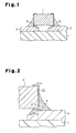
- a substrate 1 includes an upper surface on which two plate-shaped lead frames 2 and 3 are arranged spaced apart from each other. Insert molding, for example, is performed to integrally form the lead frames 2 and 3 with the substrate 1.
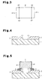
- an electrode 41 is arranged on each of the two ends of the chip capacitor 4 extending from the upper surface via the side surface to the lower surface.
- Fig. 2 shows only the right electrode 41.
- Each electrode 41 includes two opposite ends defining a first electrode portion 41 a, which is in contact with the upper surface of the chip capacitor 4, and a second electrode portion 41 b, which is in contact with a lower surface of the chip capacitor 4.
- the first electrode portion 41 a is formed by inwardly bending the first end of the electrode 41
- the second electrode portion 41 b is formed by bending the second end of the electrode 41.
- a portion of the lead frame 2 located immediately below the electrode portion 41 b defines a receiving surface 21.
- the receiving surface 21 extends from a supporting portion where the lead frame 2 would contact and support the chip capacitor 4 if there were no solder 5. Further, the receiving surface 21 extends toward the other lead frame 3 and away from the chip capacitor 4.
- the lead frame 2 includes opposite surfaces, one facing the substrate 1 and the other facing the chip capacitor 4.
- the surface facing the substrate 1 is entirely flat, and the surface facing the chip capacitor 4 includes a recess defining the receiving surface 21.
- the lead frame 3 also includes a similar recess.
- the two lead frames 2 and 3 are spaced apart from each other on the substrate 1 so that the two recesses are directed toward each other. Each recess is formed in, for example, a pressing process.
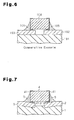
- each of the two electrode portions 41 b on the lower surface of the chip capacitor 4 has an innermost edge that includes two corners 42. Two ends of the innermost edge respectively correspond to the two corners 42 of the electrode 41 b. Two ends of outermost edge of each of the two electrode portions 41 b respectively correspond to two corners of the chip capacitor 4.
- the two electrode portions 41 b include a total of four corners 42.
- the receiving surface 21 of the lead frames 2 and 3 are formed in correspondence with the four corners 42.
- the receiving surface 21 of the lead frame 2 extends from the supporting portion, which supports the chip capacitor 4, via a portion located immediately below the two corners 42 of the electrode portion 41 b, and toward the other lead frame 3, which is paired with the lead frame 2.
- the receiving surface 21 of the lead frame 3 extends from the supporting portion, which supports the chip capacitor 4, via a portion located immediately below the two corners 42 of the electrode portion 41 b, and toward the lead frame 2.
- the solder 5 is located between each receiving surface 21 and the electrode portions 41 b. This electrically and mechanically connects the electrode portions 41 b to the lead frames 2 and 3 with a sufficient amount of the solder 5.
- insert molding is performed to integrate the lead frames 2 and 3 with the substrate 1 so that the receiving surfaces 21 and the substrate 1 are located on opposite sides of the lead frames 2 and 3.
- pellets of the solder 5 are tentatively fixed onto the lead frames 2 and 3.
- the chip capacitor 4 bridges the two lead frames 2 and 3 with the electrodes 41 contacting the solder 5.
- the pellets of the solder 5 are melted so that the melted solder 5 is partially located between the electrodes 41 of the chip capacitor 4 and the receiving surfaces 21 of the lead frames 2 and 3. This obtains the connection structure for the chip capacitor 4 shown in Fig. 1 .
- Fig. 6 shows a comparative example.
- two lead frames 102 and 103 are spaced apart on a substrate 101.
- Each of the lead frames 102 and 103 does not include the receiving surface 21.
- a chip capacitor 104 bridges the two lead frames 102 and 103.
- Solder 105 connects the chip capacitor 104 to the two lead frames 102 and 103.
- the stress generated in the solder 105 is concentrated between the chip capacitor 104 and the lead frames 102 and 103.
- the solder 105 is thin between the chip capacitor 104 and the lead frames 102 and 103.
- the receiving surface 21 is formed in each of the lead frames 2 and 3, and the solder 5 is located and received between the receiving surfaces 21 and the electrodes 41 of the chip capacitor 4.
- the stress generated in the solder 5 is concentrated between the chip capacitor 4 and the lead frames 2 and 3.
- the solder 5, which is located between the chip capacitor 4 and the lead frames 2 and 3 is thicker than the comparative example. This disperses and reduces the stress. Further, the increased amount of the solder 5 increases the strength.
- the present embodiment has the advantages described below.
- the two receiving surfaces 21 may be formed by bending the opposing ends of the two lead frames 2 and 3 toward the substrate 1 and away from the chip capacitor 4.
- the solder 5 is located between the receiving surface 21 and the electrode 41. Further, the receiving surface 21 is linearly inclined. This facilitates the positioning of the chip capacitor 4.
- the receiving surface 21 of each of the lead frames 2 and 3 may extend from the supporting portion, which supports the chip capacitor 4, to immediately below the two corners 42.
- the receiving surface 21 of the lead frames 2 and 3 may extend from the supporting portion to just before the two corners 42.
- the receiving surfaces 21 may extend continuously from the front toward the rear of the lead frames 2 and 3.
- the direction extending from the front toward the rear of each of the frames 2 and 3 is orthogonal to the direction in which the chip capacitor 4 bridges the lead frames 2 and 3.
- the inner region in the upper surface of each of the lead frames 2 and 3 excluding the receiving surface 21 defines a mounting region for the chip capacitor 4.
- four receiving surfaces 21 may be formed in four regions corresponding to the four corners 42 of the two lead frames 2 and 3.
- an inner region 25 is formed between the two receiving surfaces 21 of the lead frame 2
- an inner region 35 is formed between the two receiving surfaces 21 of the lead frame 3. This enlarges the mounting region of the chip capacitor 4 and improves the mounting stability of the chip capacitor 4.
- four receiving surfaces 21 may be formed in four regions corresponding to the four corners 42 of the two lead frames 2 and 3, and the four receiving surfaces 21 may cooperate to allow the solder 5 to be located between the four corners in the lower surface of the chip capacitor 4 and the four receiving surfaces 21.
- an inner region 25 is formed between the two receiving surfaces 21 of the lead frame 2 and an inner region 35 is formed between the two receiving surfaces 21 of the lead frame 3. This enlarges the mounting region of the chip capacitor 4 and improves the mounting stability of the chip capacitor 4.
- the solder 5 is also located immediately below the four corners in the lower surface of the chip capacitor 4. This increases the thickness of the solder 5 at these locations thereby limiting cracking.
- the electronic component is not limited to a chip capacitor 4.
- the conductive joining member is not limited to the solder 5.
- a connection structure for an electronic component which is set on two lead frames (2, 3) spaced apart from each other.
- the electronic component (4) is connected to the two lead frames (2, 3) by a conductive joining member (5).
- the connection structure includes two electrodes (41 b) arranged on at least portions of a lower surface of the electronic component (4).
- the two electrodes (41 b) respectively face the two lead frames (2, 3).
- a receiving surface (21) is included in each of the two lead frames (2, 3) immediately below the corresponding electrode (41 b).
- the receiving surface (21) extends from a supporting portion supporting the electronic component (4) toward the other one of the lead frames (2, 3) and away from the electronic component.
- the conductive joining member (5) is located between the receiving surface (21) of each of the two lead frames (2, 3) and the corresponding one of the electrodes (41 b).
Landscapes
- Engineering & Computer Science (AREA)
- Microelectronics & Electronic Packaging (AREA)
- Power Engineering (AREA)
- Manufacturing & Machinery (AREA)
- Fixed Capacitors And Capacitor Manufacturing Machines (AREA)
- Lead Frames For Integrated Circuits (AREA)
- Details Of Resistors (AREA)
Applications Claiming Priority (2)
| Application Number | Priority Date | Filing Date | Title |
|---|---|---|---|
| JP2013036232 | 2013-02-26 | ||
| JP2013190756A JP2014195039A (ja) | 2013-02-26 | 2013-09-13 | 電子部品の接続構造 |
Publications (2)
| Publication Number | Publication Date |
|---|---|
| EP2770531A2 true EP2770531A2 (de) | 2014-08-27 |
| EP2770531A3 EP2770531A3 (de) | 2016-01-27 |
Family
ID=50151186
Family Applications (1)
| Application Number | Title | Priority Date | Filing Date |
|---|---|---|---|
| EP14156313.0A Withdrawn EP2770531A3 (de) | 2013-02-26 | 2014-02-24 | Elektronische Bauteilverbindungsstruktur |
Country Status (4)
| Country | Link |
|---|---|
| US (1) | US20140240940A1 (de) |
| EP (1) | EP2770531A3 (de) |
| JP (1) | JP2014195039A (de) |
| CN (1) | CN104010439A (de) |
Cited By (1)
| Publication number | Priority date | Publication date | Assignee | Title |
|---|---|---|---|---|
| EP3109897A1 (de) * | 2015-06-23 | 2016-12-28 | Nxp B.V. | Leiterrahmenanordnung |
Families Citing this family (3)
| Publication number | Priority date | Publication date | Assignee | Title |
|---|---|---|---|---|
| US9949378B2 (en) | 2014-04-14 | 2018-04-17 | Presidio Components, Inc. | Electrical devices with solder dam |
| WO2019216161A1 (ja) * | 2018-05-09 | 2019-11-14 | 三菱電機株式会社 | パワー半導体モジュール及びその製造方法並びに電力変換装置 |
| JP7103193B2 (ja) * | 2018-12-03 | 2022-07-20 | 株式会社デンソー | 電子回路および電子回路の接合方法 |
Citations (1)
| Publication number | Priority date | Publication date | Assignee | Title |
|---|---|---|---|---|
| JP2007234737A (ja) | 2006-02-28 | 2007-09-13 | Denso Corp | 電子部品の接続構造 |
Family Cites Families (4)
| Publication number | Priority date | Publication date | Assignee | Title |
|---|---|---|---|---|
| US5804880A (en) * | 1996-11-04 | 1998-09-08 | National Semiconductor Corporation | Solder isolating lead frame |
| JP2004296624A (ja) * | 2003-03-26 | 2004-10-21 | Sanken Electric Co Ltd | 半導体装置 |
| JP4969430B2 (ja) * | 2007-12-17 | 2012-07-04 | 日立オートモティブシステムズ株式会社 | 圧力検出装置 |
| JP2009182022A (ja) * | 2008-01-29 | 2009-08-13 | Renesas Technology Corp | 半導体装置 |
-
2013
- 2013-09-13 JP JP2013190756A patent/JP2014195039A/ja active Pending
-
2014
- 2014-02-21 US US14/186,336 patent/US20140240940A1/en not_active Abandoned
- 2014-02-24 EP EP14156313.0A patent/EP2770531A3/de not_active Withdrawn
- 2014-02-24 CN CN201410062005.7A patent/CN104010439A/zh active Pending
Patent Citations (1)
| Publication number | Priority date | Publication date | Assignee | Title |
|---|---|---|---|---|
| JP2007234737A (ja) | 2006-02-28 | 2007-09-13 | Denso Corp | 電子部品の接続構造 |
Cited By (1)
| Publication number | Priority date | Publication date | Assignee | Title |
|---|---|---|---|---|
| EP3109897A1 (de) * | 2015-06-23 | 2016-12-28 | Nxp B.V. | Leiterrahmenanordnung |
Also Published As
| Publication number | Publication date |
|---|---|
| US20140240940A1 (en) | 2014-08-28 |
| EP2770531A3 (de) | 2016-01-27 |
| JP2014195039A (ja) | 2014-10-09 |
| CN104010439A (zh) | 2014-08-27 |
Similar Documents
| Publication | Publication Date | Title |
|---|---|---|
| US8282412B1 (en) | Flat cable and connection structure between flat cable and printed wiring board | |
| US11742279B2 (en) | Semiconductor device | |
| US7955118B2 (en) | Terminal plate circuit using a pressing member | |
| JP2015167225A5 (de) | ||
| CN105469995B (zh) | 固体电解电容器 | |
| US20140240940A1 (en) | Electronic component connection structure | |
| EP3213344B1 (de) | Anschlussrahmen für ein halbleiterbauelement, schaltungsanordnung mit einem anschlussrahmen | |
| US20160120024A1 (en) | Linear Conductor Connection Terminal | |
| US9595491B2 (en) | Apparatus for manufacturing semiconductor device and the semiconductor device | |
| US9793632B2 (en) | Spring finger and electrical connector | |
| KR102527716B1 (ko) | 탄탈륨 커패시터 | |
| WO2019082344A1 (ja) | 半導体装置の製造方法 | |
| JP5006744B2 (ja) | コンデンサの製造方法 | |
| CN102013578B (zh) | 导体引出结构以及功率模块 | |
| JP2009182265A (ja) | フィルムコンデンサ用電極端子及びフィルムコンデンサ | |
| KR20150054089A (ko) | 커넥터 | |
| JP2006253367A (ja) | 面実装型固体電解コンデンサとその製造方法 | |
| WO2019082343A1 (ja) | 半導体装置 | |
| CN103531934B (zh) | 连接器端子及其制造方法 | |
| JP2012234736A (ja) | 電子部品 | |
| KR101686806B1 (ko) | 와이어 터미널 | |
| JP2020072058A (ja) | コネクタ、回路基板 | |
| JP4481757B2 (ja) | 電子部品 | |
| JP6787144B2 (ja) | 半導体モジュール | |
| KR101664299B1 (ko) | 피메일 단자의 스프링 |
Legal Events
| Date | Code | Title | Description |
|---|---|---|---|
| PUAI | Public reference made under article 153(3) epc to a published international application that has entered the european phase |
Free format text: ORIGINAL CODE: 0009012 |
|
| 17P | Request for examination filed |
Effective date: 20140224 |
|
| AK | Designated contracting states |
Kind code of ref document: A2 Designated state(s): AL AT BE BG CH CY CZ DE DK EE ES FI FR GB GR HR HU IE IS IT LI LT LU LV MC MK MT NL NO PL PT RO RS SE SI SK SM TR |
|
| AX | Request for extension of the european patent |
Extension state: BA ME |
|
| PUAL | Search report despatched |
Free format text: ORIGINAL CODE: 0009013 |
|
| AK | Designated contracting states |
Kind code of ref document: A3 Designated state(s): AL AT BE BG CH CY CZ DE DK EE ES FI FR GB GR HR HU IE IS IT LI LT LU LV MC MK MT NL NO PL PT RO RS SE SI SK SM TR |
|
| AX | Request for extension of the european patent |
Extension state: BA ME |
|
| RIC1 | Information provided on ipc code assigned before grant |
Ipc: H01L 23/495 20060101AFI20151218BHEP Ipc: H01G 2/06 20060101ALI20151218BHEP |
|
| STAA | Information on the status of an ep patent application or granted ep patent |
Free format text: STATUS: THE APPLICATION IS DEEMED TO BE WITHDRAWN |
|
| 18D | Application deemed to be withdrawn |
Effective date: 20160128 |