EP2758561B1 - Coated cutting tool - Google Patents
Coated cutting tool Download PDFInfo
- Publication number
- EP2758561B1 EP2758561B1 EP12766413.4A EP12766413A EP2758561B1 EP 2758561 B1 EP2758561 B1 EP 2758561B1 EP 12766413 A EP12766413 A EP 12766413A EP 2758561 B1 EP2758561 B1 EP 2758561B1
- Authority
- EP
- European Patent Office
- Prior art keywords
- coating
- coated cutting
- cutting tool
- substrate
- deposition
- Prior art date
- Legal status (The legal status is an assumption and is not a legal conclusion. Google has not performed a legal analysis and makes no representation as to the accuracy of the status listed.)
- Active
Links
- 238000005520 cutting process Methods 0.000 title claims description 46
- 238000000576 coating method Methods 0.000 claims description 141
- 239000011248 coating agent Substances 0.000 claims description 124
- 239000000758 substrate Substances 0.000 claims description 84
- 238000005422 blasting Methods 0.000 claims description 53
- 239000010410 layer Substances 0.000 claims description 49
- 150000001875 compounds Chemical class 0.000 claims description 27
- 238000000034 method Methods 0.000 claims description 23
- 238000000541 cathodic arc deposition Methods 0.000 claims description 13
- 239000002356 single layer Substances 0.000 claims description 12
- 229910052719 titanium Inorganic materials 0.000 claims description 10
- 229910052757 nitrogen Inorganic materials 0.000 claims description 9
- 238000002441 X-ray diffraction Methods 0.000 claims description 5
- 229910052804 chromium Inorganic materials 0.000 claims description 5
- UONOETXJSWQNOL-UHFFFAOYSA-N tungsten carbide Chemical compound [W+]#[C-] UONOETXJSWQNOL-UHFFFAOYSA-N 0.000 claims description 4
- 229910052715 tantalum Inorganic materials 0.000 claims description 3
- 238000000151 deposition Methods 0.000 description 78
- 230000008021 deposition Effects 0.000 description 76
- 150000002500 ions Chemical class 0.000 description 43
- 239000000203 mixture Substances 0.000 description 19
- IJGRMHOSHXDMSA-UHFFFAOYSA-N Atomic nitrogen Chemical compound N#N IJGRMHOSHXDMSA-UHFFFAOYSA-N 0.000 description 14
- 238000010891 electric arc Methods 0.000 description 13
- 230000001965 increasing effect Effects 0.000 description 13
- 238000005259 measurement Methods 0.000 description 12
- 239000002245 particle Substances 0.000 description 12
- 239000012299 nitrogen atmosphere Substances 0.000 description 10
- 238000005240 physical vapour deposition Methods 0.000 description 10
- 238000007514 turning Methods 0.000 description 10
- 238000005229 chemical vapour deposition Methods 0.000 description 8
- 238000002203 pretreatment Methods 0.000 description 8
- 239000000523 sample Substances 0.000 description 8
- PNEYBMLMFCGWSK-UHFFFAOYSA-N aluminium oxide Inorganic materials [O-2].[O-2].[O-2].[Al+3].[Al+3] PNEYBMLMFCGWSK-UHFFFAOYSA-N 0.000 description 7
- 230000008901 benefit Effects 0.000 description 7
- 229910000831 Steel Inorganic materials 0.000 description 6
- 230000000694 effects Effects 0.000 description 6
- 239000010959 steel Substances 0.000 description 6
- 230000008859 change Effects 0.000 description 5
- 238000005137 deposition process Methods 0.000 description 5
- 239000007789 gas Substances 0.000 description 5
- 230000013011 mating Effects 0.000 description 5
- 230000008569 process Effects 0.000 description 5
- 239000013077 target material Substances 0.000 description 5
- 239000000463 material Substances 0.000 description 4
- 238000001000 micrograph Methods 0.000 description 4
- ATJFFYVFTNAWJD-UHFFFAOYSA-N Tin Chemical compound [Sn] ATJFFYVFTNAWJD-UHFFFAOYSA-N 0.000 description 3
- 230000032798 delamination Effects 0.000 description 3
- 230000005672 electromagnetic field Effects 0.000 description 3
- 238000002149 energy-dispersive X-ray emission spectroscopy Methods 0.000 description 3
- 230000003628 erosive effect Effects 0.000 description 3
- 229910052720 vanadium Inorganic materials 0.000 description 3
- 229910052582 BN Inorganic materials 0.000 description 2
- PZNSFCLAULLKQX-UHFFFAOYSA-N Boron nitride Chemical compound N#B PZNSFCLAULLKQX-UHFFFAOYSA-N 0.000 description 2
- AFCARXCZXQIEQB-UHFFFAOYSA-N N-[3-oxo-3-(2,4,6,7-tetrahydrotriazolo[4,5-c]pyridin-5-yl)propyl]-2-[[3-(trifluoromethoxy)phenyl]methylamino]pyrimidine-5-carboxamide Chemical compound O=C(CCNC(=O)C=1C=NC(=NC=1)NCC1=CC(=CC=C1)OC(F)(F)F)N1CC2=C(CC1)NN=N2 AFCARXCZXQIEQB-UHFFFAOYSA-N 0.000 description 2
- MCMNRKCIXSYSNV-UHFFFAOYSA-N Zirconium dioxide Chemical compound O=[Zr]=O MCMNRKCIXSYSNV-UHFFFAOYSA-N 0.000 description 2
- 238000004458 analytical method Methods 0.000 description 2
- 239000012298 atmosphere Substances 0.000 description 2
- 230000007547 defect Effects 0.000 description 2
- 238000000280 densification Methods 0.000 description 2
- 238000013461 design Methods 0.000 description 2
- 230000001627 detrimental effect Effects 0.000 description 2
- 238000009826 distribution Methods 0.000 description 2
- 230000004907 flux Effects 0.000 description 2
- 238000007373 indentation Methods 0.000 description 2
- 238000010849 ion bombardment Methods 0.000 description 2
- 230000001788 irregular Effects 0.000 description 2
- 238000003754 machining Methods 0.000 description 2
- 238000004519 manufacturing process Methods 0.000 description 2
- 238000000399 optical microscopy Methods 0.000 description 2
- 229910001220 stainless steel Inorganic materials 0.000 description 2
- 239000010935 stainless steel Substances 0.000 description 2
- 230000001960 triggered effect Effects 0.000 description 2
- 238000009827 uniform distribution Methods 0.000 description 2
- BWSQKOKULIALEW-UHFFFAOYSA-N 2-[2-[4-fluoro-3-(trifluoromethyl)phenyl]-3-[2-(piperidin-3-ylamino)pyrimidin-4-yl]imidazol-4-yl]acetonitrile Chemical compound FC1=C(C=C(C=C1)C=1N(C(=CN=1)CC#N)C1=NC(=NC=C1)NC1CNCCC1)C(F)(F)F BWSQKOKULIALEW-UHFFFAOYSA-N 0.000 description 1
- 229910000997 High-speed steel Inorganic materials 0.000 description 1
- 229910052774 Proactinium Inorganic materials 0.000 description 1
- 229910001083 Sverker 21 Inorganic materials 0.000 description 1
- 229910001315 Tool steel Inorganic materials 0.000 description 1
- ODUIXUGXPFKQLG-QWRGUYRKSA-N [2-(4-chloro-2-fluoroanilino)-5-methyl-1,3-thiazol-4-yl]-[(2s,3s)-2,3-dimethylpiperidin-1-yl]methanone Chemical compound C[C@H]1[C@@H](C)CCCN1C(=O)C1=C(C)SC(NC=2C(=CC(Cl)=CC=2)F)=N1 ODUIXUGXPFKQLG-QWRGUYRKSA-N 0.000 description 1
- 230000002730 additional effect Effects 0.000 description 1
- 238000013459 approach Methods 0.000 description 1
- 229910000963 austenitic stainless steel Inorganic materials 0.000 description 1
- 230000015572 biosynthetic process Effects 0.000 description 1
- 239000000919 ceramic Substances 0.000 description 1
- 239000011195 cermet Substances 0.000 description 1
- 239000011247 coating layer Substances 0.000 description 1
- 230000006835 compression Effects 0.000 description 1
- 238000007906 compression Methods 0.000 description 1
- 230000003247 decreasing effect Effects 0.000 description 1
- 230000001419 dependent effect Effects 0.000 description 1
- 230000002542 deteriorative effect Effects 0.000 description 1
- 229910003460 diamond Inorganic materials 0.000 description 1
- 239000010432 diamond Substances 0.000 description 1
- 238000006073 displacement reaction Methods 0.000 description 1
- 238000005553 drilling Methods 0.000 description 1
- 230000005684 electric field Effects 0.000 description 1
- 230000002708 enhancing effect Effects 0.000 description 1
- 230000008020 evaporation Effects 0.000 description 1
- 238000001704 evaporation Methods 0.000 description 1
- 239000012530 fluid Substances 0.000 description 1
- 238000005286 illumination Methods 0.000 description 1
- 238000005305 interferometry Methods 0.000 description 1
- 238000012804 iterative process Methods 0.000 description 1
- 238000003801 milling Methods 0.000 description 1
- 238000012986 modification Methods 0.000 description 1
- 230000004048 modification Effects 0.000 description 1
- 238000012544 monitoring process Methods 0.000 description 1
- 229910052758 niobium Inorganic materials 0.000 description 1
- 230000003287 optical effect Effects 0.000 description 1
- 230000000737 periodic effect Effects 0.000 description 1
- 238000001020 plasma etching Methods 0.000 description 1
- 239000000843 powder Substances 0.000 description 1
- 230000008707 rearrangement Effects 0.000 description 1
- 229920006395 saturated elastomer Polymers 0.000 description 1
- 238000001878 scanning electron micrograph Methods 0.000 description 1
- 238000005480 shot peening Methods 0.000 description 1
- HBMJWWWQQXIZIP-UHFFFAOYSA-N silicon carbide Chemical compound [Si+]#[C-] HBMJWWWQQXIZIP-UHFFFAOYSA-N 0.000 description 1
- 229910010271 silicon carbide Inorganic materials 0.000 description 1
- 238000004544 sputter deposition Methods 0.000 description 1
- 230000003746 surface roughness Effects 0.000 description 1
- 238000002207 thermal evaporation Methods 0.000 description 1
Images


Classifications
-
- C—CHEMISTRY; METALLURGY
- C23—COATING METALLIC MATERIAL; COATING MATERIAL WITH METALLIC MATERIAL; CHEMICAL SURFACE TREATMENT; DIFFUSION TREATMENT OF METALLIC MATERIAL; COATING BY VACUUM EVAPORATION, BY SPUTTERING, BY ION IMPLANTATION OR BY CHEMICAL VAPOUR DEPOSITION, IN GENERAL; INHIBITING CORROSION OF METALLIC MATERIAL OR INCRUSTATION IN GENERAL
- C23C—COATING METALLIC MATERIAL; COATING MATERIAL WITH METALLIC MATERIAL; SURFACE TREATMENT OF METALLIC MATERIAL BY DIFFUSION INTO THE SURFACE, BY CHEMICAL CONVERSION OR SUBSTITUTION; COATING BY VACUUM EVAPORATION, BY SPUTTERING, BY ION IMPLANTATION OR BY CHEMICAL VAPOUR DEPOSITION, IN GENERAL
- C23C14/00—Coating by vacuum evaporation, by sputtering or by ion implantation of the coating forming material
- C23C14/06—Coating by vacuum evaporation, by sputtering or by ion implantation of the coating forming material characterised by the coating material
- C23C14/0641—Nitrides
-
- B—PERFORMING OPERATIONS; TRANSPORTING
- B23—MACHINE TOOLS; METAL-WORKING NOT OTHERWISE PROVIDED FOR
- B23B—TURNING; BORING
- B23B27/00—Tools for turning or boring machines; Tools of a similar kind in general; Accessories therefor
- B23B27/14—Cutting tools of which the bits or tips or cutting inserts are of special material
- B23B27/148—Composition of the cutting inserts
-
- C—CHEMISTRY; METALLURGY
- C23—COATING METALLIC MATERIAL; COATING MATERIAL WITH METALLIC MATERIAL; CHEMICAL SURFACE TREATMENT; DIFFUSION TREATMENT OF METALLIC MATERIAL; COATING BY VACUUM EVAPORATION, BY SPUTTERING, BY ION IMPLANTATION OR BY CHEMICAL VAPOUR DEPOSITION, IN GENERAL; INHIBITING CORROSION OF METALLIC MATERIAL OR INCRUSTATION IN GENERAL
- C23C—COATING METALLIC MATERIAL; COATING MATERIAL WITH METALLIC MATERIAL; SURFACE TREATMENT OF METALLIC MATERIAL BY DIFFUSION INTO THE SURFACE, BY CHEMICAL CONVERSION OR SUBSTITUTION; COATING BY VACUUM EVAPORATION, BY SPUTTERING, BY ION IMPLANTATION OR BY CHEMICAL VAPOUR DEPOSITION, IN GENERAL
- C23C14/00—Coating by vacuum evaporation, by sputtering or by ion implantation of the coating forming material
- C23C14/22—Coating by vacuum evaporation, by sputtering or by ion implantation of the coating forming material characterised by the process of coating
- C23C14/24—Vacuum evaporation
- C23C14/32—Vacuum evaporation by explosion; by evaporation and subsequent ionisation of the vapours, e.g. ion-plating
- C23C14/325—Electric arc evaporation
-
- C—CHEMISTRY; METALLURGY
- C23—COATING METALLIC MATERIAL; COATING MATERIAL WITH METALLIC MATERIAL; CHEMICAL SURFACE TREATMENT; DIFFUSION TREATMENT OF METALLIC MATERIAL; COATING BY VACUUM EVAPORATION, BY SPUTTERING, BY ION IMPLANTATION OR BY CHEMICAL VAPOUR DEPOSITION, IN GENERAL; INHIBITING CORROSION OF METALLIC MATERIAL OR INCRUSTATION IN GENERAL
- C23C—COATING METALLIC MATERIAL; COATING MATERIAL WITH METALLIC MATERIAL; SURFACE TREATMENT OF METALLIC MATERIAL BY DIFFUSION INTO THE SURFACE, BY CHEMICAL CONVERSION OR SUBSTITUTION; COATING BY VACUUM EVAPORATION, BY SPUTTERING, BY ION IMPLANTATION OR BY CHEMICAL VAPOUR DEPOSITION, IN GENERAL
- C23C14/00—Coating by vacuum evaporation, by sputtering or by ion implantation of the coating forming material
- C23C14/58—After-treatment
- C23C14/5886—Mechanical treatment
-
- H—ELECTRICITY
- H01—ELECTRIC ELEMENTS
- H01J—ELECTRIC DISCHARGE TUBES OR DISCHARGE LAMPS
- H01J37/00—Discharge tubes with provision for introducing objects or material to be exposed to the discharge, e.g. for the purpose of examination or processing thereof
- H01J37/32—Gas-filled discharge tubes
- H01J37/32009—Arrangements for generation of plasma specially adapted for examination or treatment of objects, e.g. plasma sources
- H01J37/32055—Arc discharge
-
- B—PERFORMING OPERATIONS; TRANSPORTING
- B23—MACHINE TOOLS; METAL-WORKING NOT OTHERWISE PROVIDED FOR
- B23B—TURNING; BORING
- B23B2224/00—Materials of tools or workpieces composed of a compound including a metal
- B23B2224/24—Titanium aluminium nitride
-
- B—PERFORMING OPERATIONS; TRANSPORTING
- B23—MACHINE TOOLS; METAL-WORKING NOT OTHERWISE PROVIDED FOR
- B23B—TURNING; BORING
- B23B2228/00—Properties of materials of tools or workpieces, materials of tools or workpieces applied in a specific manner
- B23B2228/10—Coatings
- B23B2228/105—Coatings with specified thickness
-
- Y—GENERAL TAGGING OF NEW TECHNOLOGICAL DEVELOPMENTS; GENERAL TAGGING OF CROSS-SECTIONAL TECHNOLOGIES SPANNING OVER SEVERAL SECTIONS OF THE IPC; TECHNICAL SUBJECTS COVERED BY FORMER USPC CROSS-REFERENCE ART COLLECTIONS [XRACs] AND DIGESTS
- Y10—TECHNICAL SUBJECTS COVERED BY FORMER USPC
- Y10T—TECHNICAL SUBJECTS COVERED BY FORMER US CLASSIFICATION
- Y10T407/00—Cutters, for shaping
- Y10T407/27—Cutters, for shaping comprising tool of specific chemical composition
Definitions
- the present invention relates to a coated cutting tool comprising a substrate and a comparatively thick PVD coating.
- CVD chemical vapor deposition
- PVD physical vapor deposition
- US 7,838,132 discloses cathodic arc deposition of about 3 ⁇ m thick (Ti,Al)N coatings on cemented carbide substrates using an arc current of 200 A at different substrate bias ranging from -40 V to -200 V and concludes that there is an optimum at about -70 V where high compressive stresses, i.e. more than 4 GPa, and still good adhesion can be achieved.
- Other sophisticated biasing techniques may enable stress relief and bond rearrangement during deposition and thereby allowing a comparatively high kinetic energy without severely suffering from delamination problems.
- US2010/0215912 is concerned with providing hard-coated members having a thick coating having a reduced compression stress, in order to obtain high adhesion and chipping resistance.
- US2010/0260561 discloses coated cutting tools, in which the integrated internal stress at the surface region of the coating is adjusted to a particular range in order to improve the properties of the coating.
- One object of the invention is to improve wear resistance of coated cutting tools without deteriorating other properties such as flaking resistance.
- a further object is to provide a PVD coated tool suitable for turning in steel and other applications in which CVD coatings typically are used. This is accomplished by a coated cutting tool as defined by claim 1.
- a coated cutting tool in accordance with the invention comprises a substrate and a coating, where the coating comprises at least one compound layer deposited by cathodic arc deposition and has a thickness of more than 15 ⁇ m and up to 30 ⁇ m.
- thicknesses is for this purpose meant the thickness on the side of the coated cutting tool, i.e. either a flank side or a rake side, which has the thickest coating.
- the thickness is measured, preferably by light optical microscopy on polished cross sections, about 0.2 mm from the edge line.
- the thicknesses given herein refers to the thickness measured on any reasonably flat surface or a surface having a relatively large curvature and some distance away from any edge or corner.
- the thickness exceeds coating thicknesses of state-of-the-art coated cutting tools produced by PVD and thereby gives superior crater wear resistance while still performing as good or better with respect to flank wear and flaking.
- the compound layer comprises Al, and N.
- the compound layer has hard wear resistance, in particular with good abrasive wear resistance.
- the compound layer may be provided in the form of a single layer or a multi-layer structure.
- multilayer structure is herein meant a stack of individual layers, at least 5 up to several thousand individual layers, preferably comprising at least two repeatedly alternating individual layers having different properties with respect to e.g. composition. The repetition may be periodic or aperiodic.
- the single layer has substantially the same properties throughout the thickness of the single layer.
- one or more properties may be varied continuously in part or throughout the thickness of the single layer, the individual layer of the multi-layer structure or the multi-layer structure.
- a compositional gradient may be formed.
- composition is herein meant the composition measured on a section of a cross section of the coating.
- EDS Energy-dispersive X-ray Spectroscopy
- the spatial resolution of the measurement may not be enough to resolve the composition of individual layers of a multi-layer structure without contribution from adjacent layers due to low layer thickness.
- What can readily be measured is the average composition over a section of the multi-layer structure including more than one individual layer.
- the compound layer is a single layer of Ti 1-x Al x N with an average composition of 0.5 ⁇ x ⁇ 0.7.
- the compound layer is a single layer of Ti 1-x Al x N with an average composition of 0.3 ⁇ x ⁇ 0.5.
- the substrates of embodiments of the invention are uncoated or coated cutting tools, like cutting tool inserts, round tools such as drills, end mills, taps etc, and is made of any material known to be used in these applications such as cemented carbide, cermets, ceramics, cubic boron nitride, polycrystalline diamond or high-speed steels. More preferably the substrate is made of cemented carbide, cermet or cubic boron nitride since these materials have thermal and mechanical properties that are essential to fully benefit from the advantageous properties of the coating layer deposited on the substrate such that the coated cutting tool obtain excellent wear resistance and toughness.
- a cemented carbide substrate in accordance with one embodiment of the invention preferably comprises 5-13.5 wt-% Co and balance tungsten carbide (WC). Additionally, the elements Ti, Ta, V, Cr, Nb may be present.
- a cemented carbide substrate in accordance with one embodiment of the invention preferably comprises tungsten carbide (WC) with a sub-micron grain size, 5-13,5 wt-% Co, preferably 6-10 wt-% Co, and Cr such that the Cr/Co ratio by weight is 0.04-0.15, and balance WC.
- ppm levels of the elements Ti, Ta, or V Preferably, the coercivity, He, of this fine-grained substrate ranges from 18-30 kA/m.
- the hardness of the substrate, HV3 is from 1500 up to 2200 kgf/mm 2 , more preferably 1800-2200 kgf/mm 2 .
- the stress state of the compound layer and thereby the coating of the coated cutting tool in accordance with the invention is preferably controlled by means of deposition parameters and blasting as explained in the following.
- the blasting has the additional effect that it smoothens the as-deposited coating.
- the coating has an internal compressive stress ranging from higher than 1.3 to 2 GPa as determined by X-ray diffraction analysis.
- the surface areal roughness of the coating as measure by white light optical interferometry can be defined by standardized surface texture parameters (ISO 25178).
- the surface texture parameter Sa defining the arithmetical mean height of the surface, is less than 0.4 ⁇ m, preferably less than 0.3 ⁇ m.
- the surface texture is further characterized in that the surface texture parameter Spd, defining the density of peaks, is less than 10x10 3 /mm 2 .
- the surface texture is further characterized in that the surface texture parameter Sdr, defining the developed area ratio, is less than 10%, preferably less than 6%.
- the internal stress, ⁇ , of the coating of embodiments of the invention is evaluated by X-ray diffraction measurements using the well-known sin 2 ⁇ method as described by I.C. Noyan, J.B. Cohen, Residual Stress Measurement by Diffraction and Interpretation, Springer-Verlag, New York, 1987 (pp 117-130 ).
- the measurements shall be performed using CuK ⁇ -radiation on the (Ti,Al)N (200) reflection. It is recommended to use the side-inclination technique ( ⁇ -geometry) with six to eleven, preferably eight, ⁇ -angles, equidistant within a selected sin 2 ⁇ -range.
- Young's modulus, E can be determined e.g. by nano-indentation technique.
- the data are evaluated using commercially available software such as DIFFRAC Plus Stress32 v. 1.04 from Bruker AXS preferably locating the (200) reflection by the Pseudo-Voigt-Fit function.
- DIFFRAC Plus Stress32 v. 1.04 from Bruker AXS preferably locating the (200) reflection by the Pseudo-Voigt-Fit function.
- the total stress is calculated as the average of the obtained biaxial stresses.
- the coating has a compressive stress being higher than 1.3 GPa. By increasing the compressive stress, the toughness can be improved.
- the coating has a compressive stress being lower than 2 GPa. Thanks to this limitation of the compressive stresses in the coating and the advantageous properties of the cathodic arc deposition process a combination of high wear resistance and high flaking resistance can be obtained.
- the internal stress of the coating is controlled to benefit from the effect of compressive stresses without suffering from delamination problems due to the thickness of the coating.
- the thickness of the coating is more than 20 ⁇ m.
- the compound layer of the coating is a single layer of Ti 1-X Al X N with an average composition of 0.5 ⁇ x ⁇ 0.7, the coating having compressive stress ranging from 1.3GPa to 2GPa.
- the coating preferably has a predominant (200) texture, i.e. the intensity of (200) is significantly higher than the intensity of (111) as measured by X-ray diffraction.
- the surface areal roughness is smooth, i.e. Sa, is less than 0.4 ⁇ m, preferably less than 0.3 ⁇ m, Spd, is less than 10x10 3 /mm 2 , and Sdr, is less than 10%, preferably less than 6%.
- the substrate is made of cemented carbide, more preferably a fine-grained cemented carbide.
- cemented carbide more preferably a fine-grained cemented carbide.
- This embodiment gives unexpected good result with respect to crater wear, flank wear and flaking.
- the compound layer is a single layer of Ti 1-X Al X N with an average composition of 0.3 ⁇ x ⁇ 0.5, otherwise the same properties as the previous embodiment.
- the compound layer comprises a gradient with respect to the internal stress within the coating. This gradient can be determined by control of the deposition conditions and/or the post-treatment blasting.
- the bias voltage can be varied during deposition to accomplish an internal stress gradient, by way of example linearly increasing the bias voltage yielding a substantially linear change in internal stress towards higher compressive stress towards the outer surface of the compound layer or the bias voltage can be increased exponentially yielding a steep increase of the internal stress towards higher compressive stress in the outermost part of the compound layer whereas the compressive stress in the inner part of the compound layer is low or even tensile.
- the compound layer may be an innermost layer, closest to the substrate. It may also be an outermost layer of the coating.
- the coating may comprise of more layers than said at least one compound layer, such as one or more intermediate layers between the substrate and the compound layer or an outermost layer deposited on the compound layer.
- PVD coated cutting tool insert that outperforms conventional PVD coated cutting tools with respect to crater wear, flank wear without suffering from flaking and that has a crater wear resistance comparable to a state-of-the-art CVD coated cutting tool.
- a method for cathodic arc deposition within a vacuum chamber of a coating comprising at least on compound layer on a substrate in accordance with the invention comprises generating a plasma from an arc discharge visible as one or more arc spots on a surface of a plate-shaped target by applying an arc current of at least 200 A between the plate-shaped target, which acts a cathode, and an anode arrangement such that ions of the arc discharge are emitted out from the plate-shaped target to contribute in forming the coating the substrate.
- an ion current density at the surface of the substrate to be coated is of significant importance for the properties of the coating.
- One measure of the ion current density is the total ion current produced by one or more plate-shaped targets.
- the total ion current can be estimated by measuring the ion current density with a probe surface negatively biased relative a voltage potential of the anode arrangement and facing the plate-shaped target at a distance of about 15 cm from the target surface and multiplying the measured ion current density with the total surface area of the plate-shaped target.
- the total ion current is at least 5 A.
- the surface area of the plate-shaped target is preferably larger than 500 cm 2 , more preferably larger than 1000 cm 2 .
- branching of the arc discharge into a multitude of arc spots distributed over substantially the whole surface area of the target is possible.
- the branching is promoted by the high arc current.
- One advantage of the branching is that it gives a comparatively uniform ion current density in the plasma over the whole surface area of the target. This can be observed as a substantially uniform illumination of the target surface during deposition.
- Another advantage of the branching is that it enables improved target utilization.
- Yet another advantage is that it is possible to obtain uniform deposition conditions in the whole vacuum chamber and hence uniform coating thickness and properties within a batch of substrates to be coated.
- the measured ion current density which is measured at saturation conditions of the current, is larger than 6 mA/cm 2 , more preferably larger than 10 mA/cm 2 , and even more preferably between 6 mA/cm 2 to 16 mA/cm 2 in order to obtain the high total ion current and to get a high ion flux at the substrates.
- Additional plate-shaped targets may be provided, e.g. to further increase ion current supplied to the plasma formed, or to provide plate-shaped targets with different composition.
- the arc discharge supplies ions to the plasma.
- One measure of the amount of ions that are supplied to the plasma is the total ion current from the plate-shaped target as defined above.
- the supply of ions can be determined by summarizing the total ion current from each of the plate-shaped targets.
- the sum of total ion currents from a respective plate-shaped target divided by the volume of the vacuum chamber is at least 3 A/m 3 .
- the method comprises applying a voltage potential difference between the substrate and the plate-shaped target, i.e. a bias voltage V s to the substrate being negative relative a voltage potential V A of the anode arrangement and a cathode voltage Vc being negative relative the voltage potential V A of the anode arrangement.
- a bias voltage V s to the substrate being negative relative a voltage potential V A of the anode arrangement and a cathode voltage Vc being negative relative the voltage potential V A of the anode arrangement.
- V S - V C ⁇ 0 V.
- -19 V ⁇ V C - V A ⁇ -15V preferably -18 V ⁇ V C - V A ⁇ -16V.
- -30 V ⁇ V S - V A ⁇ -15 V preferably -25 V ⁇ V S - V A ⁇ -15 V.
- the bias voltage Vs is intended to be a peak voltage.
- Ions impinging on the substrate will due to the comparatively low voltage biasing of the substrate have a moderate kinetic energy, contrary to the above-mentioned prevalent strive to increase the kinetic energy of the ions in order to increase ion mobility and thereby improve mechanical properties.
- a high ion flux is provided at the surface of the substrate such that the total energy transferred from ions arriving at the substrate surface is still high thereby enhancing ion mobility at the surface which improves the mechanical properties without introducing detrimental high stress levels and/or defects in the coating. Thereby the stress state in the coating can be efficiently controlled.
- the total ion current increases and the deposition rate increases.
- the increase of the current also promotes branching of the arc discharge.
- the arc current that generates the arc plasma is at least 400 A per plate-shaped target, preferably at least 800 A, more preferably 400-1200 A.
- a deposition system for depositing a coating in accordance the invention preferably comprises an anode arrangement comprising an anode member with an anode surface directed towards the plate-shaped target and arranged concentrically with each plate-shaped target and extending laterally along a rim thereof.
- the large anode surface is provided close to the target and the anode surface area is fairly constant along the whole length of the plate-shaped target in order to provide uniform plasma conditions along the whole length, irrespective of conditions elsewhere in the vacuum chamber.
- the anode member is preferably substantially interrupted in a section of the rim extending at least partly along the width of the target on each side of the plate-shaped target in the end portions thereof in order to tailor the shape and size of the anode surface such that the plasma conditions are uniform also in the end portions.
- the anode member may further comprise an anode surface that tapers outwards as the anode member extends away from the plate-shaped target in the normal direction thereof.
- the anode member of the present invention may further serve to contribute to a balanced electromagnetic field over the whole plate-shaped target.
- This total electromagnetic field is further influenced by a magnetic self-field originating from the arc current, a magnetic field originating from the means for generating a magnetic field, and a magnetic field originating from current mating of the plate-shaped target.
- the balanced electromagnetic field is that the erosion of the plate-shaped targets becomes uniform and the target utilization is improved as compared to conventional deposition systems, in particular for high arc currents above 200 A.
- the deposition system may further comprise means for generating a lateral magnetic field on the target surface.
- This lateral magnetic field can be used to steer the displacement of the arc spot(s) of the arc plasma.
- the magnetic field originating from means for generating a magnetic field is moderate, preferably less than 100 Gauss, more preferably 5-40 Gauss. This results in a weak steering of the arc discharge, i.e. branches of the arc discharge, around the plate-shaped target.
- the impedance which is determined by measuring the average voltage and arc current over the anode arrangement and the plate-shaped target, is preferably controlled to be within a predetermined range, preferably less than 0.1 Ohm, more preferably less than 0.05 Ohm, during deposition. This is accomplished at least partly by using a comparatively weak lateral magnetic field for steering the arc discharge, contrary to steered arc techniques where a strong magnetic field is used. These steered arc techniques are conventional ways to slightly increase the arc current, however not readily above 200 A, without impairing the coating properties by increased droplet formation.
- the arc current can be increased to give effective multi-branching of the arc discharge and a dense plasma in order to give a high deposition rate and without impairing coating properties.
- the impedance is not only determined by the magnetic field applied, but also other parameters such as anode placement, anode design, gas pressure, cathode design, etc. Therefore, all parameters should be considered when limiting the impedance.
- Weak magnetic steering and well-defined electrical field between anode and cathode improve target utilization since it prevents problems associated with random arc and conventional steered arc techniques. For example, as compared to the latter the typical race track in the target is prevented due to uniform distribution of arc spots and efficient branching of the arc over the target surface.
- the anode current density around the target can be kept constant, which enables higher currents and uniform erosion around the target.
- the method may further comprise changing the voltage bias gradually during deposition to control the internal stress of the compound layer.
- the voltage bias is increased during deposition.
- the voltage bias may be increased linearly, or progressively, e.g. exponentially.
- deposition is performed until a thick coating has been formed, at least 15 ⁇ m, preferably at least 20 ⁇ m.
- the deposition process can be varied to accomplish single-layered or multi- layered coatings.
- Multilayer structures can be accomplished by methods known in the art, by way of example targets of different composition and rotating the substrates to be coated in front of the targets.
- the method may further comprise different pre -treatment or post-treatment steps.
- One example is a pre -treatment comprising subjecting the substrate blasting, preferably a two-step blasting operation including a first dry blasting step to provide an edge rounding of the substrate followed by a second wet blasting step to remove residues from the dry blasting step.
- the blasting can be performed with either dry blasting or wet basting as well.
- the parameters for pre-treatment blasting can be varied and is well known to a person skilled in the art.
- the coating formed by one or more of the above described steps is subjected to a post-treatment comprising blasting, alternatively shot-peening or the like.
- the blasting may provide a smoother surface.
- the blasting may change the stress state in the coating, e.g. increasing the compressive stresses in the coating. Both aspects may contribute to an improved performance of the coated cutting tool formed by deposition in accordance with embodiment of the invention, in particular for thick coatings. Due to a combination controlling the stress state using the deposition parameters, such as the pressure, the ion current density and the bias, and the post-treatment blasting control of the stress state of the coating can be improved which yields an unexpected good performance of the coated cutting tool.
- the coating is subjected to wet blasting using a nozzle arranged at a distance of about 20-300 mm, preferably 40-200 mm, and an angle of about 0-90°, preferably 35-65°, relative the rake side of the substrate and 100-800 mesh particles, preferably 300-500 mesh, at a pressure of about 0.1-0.6 MPa.
- the duration of the wet blasting of the coating is preferably about 0.5-1 minutes.
- Suitable particles to be used includes, however not limited to, alumina, silicon carbide and zirconia.
- a blasting medium such as particles
- the blasting may be performed either under dry conditions, i.e. with the particles or the like as a powder, or wet conditions, i.e. with the particles or the like suspended in a fluid.
- the blasting process may for example be adjusted to smoothen or roughen the surface of the substrate.
- the blasting can also change the stress state of the as-deposited coating. As appreciated by one skilled in the art this change can be tailored by e.g. selecting particular blasting medium, duration, angle, pressure etc.
- the deposition process may comprises different plasma etching steps, prior to, during or subsequent to deposition of the compound layer or individual layers thereof.
- FIG. la schematically illustrates one example of deposition system for cathodic arc deposition of a coating in accordance with the invention.
- Fig. 1b shows front view and top view of a plate-shaped target 1 and an anode member.
- the manufacturing of the coating is herein described with reference to this non-limiting example, however, as appreciated by one skilled in the art, the deposition system can be modified in different ways.
- the deposition of the coating is performed within a vacuum chamber 3 coupled to vacuum pumps (not shown) to control the pressure within the vacuum chamber 3.
- One or more plate-shaped targets 1 acting as sources of coating material in the deposition process are provided in or on the walls of the vacuum chamber 3 with their target surfaces facing the interior of the vacuum chamber 3.
- the plate-shaped targets 1 and an anode arrangement, preferably including the anode member 2, are connected to an arc power supply (not shown) and form cathode and anode of the deposition system, respectively.
- An arc discharge is used to evaporate target material.
- the arc discharge is triggered by a trigger (not shown).
- a substrate 5 to be coated is preferably carried by a fixture 6 in the vacuum chamber 3 in line-of-sight from the plate-shape targets 1. In order to uniformly coat all sides of the substrate 5 the fixture may be rotatable.
- the substrates 5 may be connected via the fixture 6 to a bias voltage power supply.
- the deposition may be performed in a reactive atmosphere such that evaporated target material and a reactive gas supplied through a gas inlet into the vacuum chamber 3 react to form a compound coating.
- the bias voltage can be provided by a bias voltage power supply.
- the bias voltage may be a DC voltage or a pulsed voltage.
- the bias voltage power supply comprises a pulse generating unit.
- the bias voltage power supply is preferably connected to a control unit that monitors the bias voltage output from the bias voltage power supply during deposition and adjusts the power supply to obtain the desired bias voltage level.
- the arc current is a direct current supplied by a power supply connected to the deposition system.
- the direct current is not necessarily constant over time. Although the arc current may show considerable variation during deposition due to individual contribution from the short-lived arc discharges, this direct current should not be mixed-up with pulsed deposition techniques. Pulsed deposition can be used for the same reasons as in prior art deposition processes.
- the deposition system may comprise a control unit and an impedance monitoring unit, arranged such that the control unit based on the measurement of the impedance between the anode and the plate-shaped target by the impedance control unit adjusts the magnitude of the lateral magnetic field generated by means for generating a lateral magnetic field in order to keep the impedance within a predetermined range.
- the control unit may be automatically or manually controlled.
- Balancing of magnetic self-field originating from arc current, magnetic field originating from means for generating a magnetic field, and a magnetic field originating from current mating of the target is preferably performed by an empirical, iterative process aiming at accomplishing a uniform distribution of the arc spots over the whole surface of the plate-shaped target.
- Balancing of non-uniform magnetic fields originating from the current mating can be accomplished by providing an asymmetric distribution of permanent magnets under the plate-shaped target.
- a cathode arrangement of a deposition system may comprise plate-shaped target arranged on a conductive back plate.
- the back plate may comprise at least two current bars running along the length thereof. These current bars are connected to the arc power supply in opposite ends of the plate-shaped target and current. Hence the arc current enters the current bars from opposite ends of the plate-shaped target and is spread via the current bars and the conductive back plate to the plate-shaped target.
- the current density in each current bar is higher close to the current input to the current bar and is depleted towards the opposite end. Consequently, the magnetic field originating from the current mating through the current bars is also decreasing along the current bar.
- the effect of this can be balanced using asymmetrically distributed permanent magnets arranged such that the magnetic field around the plate-shaped target becomes uniform.
- FIG. la schematically illustrates a side view of the anode member used in the following examples.
- FIG. 1b schematically illustrates front view and top view of the anode member and the plate-shaped target.
- the anode member is substantially interrupted in a section extending at least partly along the width of the plate-shaped target in opposite end portions of the plate-shaped target. Further the anode member comprises an anode surface that tapers outwards as the anode member extends away from the plate-shaped target in the normal direction thereof.
- Examples 1, 5, 6 (before blasting) and 7 disclose embodiments of the invention and Examples 8-10 disclose reference samples representing state-of-the-art, which in Examples 11 -13 are compared with respect to crater wear, flank wear and flaking. Examples 2-4 and are provided for information. Substantially the same deposition process has been used for all the samples of Examples 1-7 and is described hereinafter.
- the coatings of Examples 1-7 were deposited on a substrate using a cathodic arc deposition system comprising one or more comparatively large plate-shaped targets as described above.
- the substrate 5 to be coated is carried by a fixture 6 in line-of-sight from the plate-shape targets 1. In order to uniformly coat all sides of a substrate 5 the fixture is rotatable.
- the substrates 5 are connected via the fixture 6 to a bias voltage power supply.
- the deposition is performed in a reactive atmosphere such that evaporated target material and a reactive gas supplied through a gas inlet into the vacuum chamber 3 react to form a compound coating.
- the substrates used in the examples are all CNMG120408 inserts of three different compositions, hereinafter referred to as substrates SI, S2 and S3, respectively. These substrates are specified in Table 1.
- the coercivity value, He was measured using a Foerster Koerzimat CS1.096 according to DIN IEC 60404-7.
- a (Ti,Al)N coating was deposited on a SI substrate in a nitrogen atmosphere using five plate-shaped targets, each plate-shaped target comprising 40 at-% Ti and 60 at-% Al.
- the substrate Prior to loading the substrate into the deposition system, the substrate was subjected to dry blasting to obtain a honing to an edge radius of 30-60 ⁇ m followed by wet blasting to clean the substrate from residues from the dry blasting step.
- the dry blasting was performed using a nozzle with diameter 10 mm arranged at a distance of about 150 mm and an angle of about 45° relative the rake side of the substrate and 100 mesh alumina particles at a pressure of about 0.4-0.6 MPa, i.e. the particles impinging with a 45° angle on the rake side of the substrate.
- the wet blasting was performed using a nozzle with diameter 9.5 mm arranged at a distance of about 150 mm and an angle of about 45° relative the rake side of the substrate and 360 mesh alumina particles at a pressure of about 0.4 MPa.
- the duration of the wet blasting of the substrate was about 0.5-1 minutes.
- the substrate was horizontally arranged, i.e. with their flank faces facing the plate-shaped targets, on fixtures enabling threefold rotation in the deposition system.
- the substrate Prior to deposition the substrate was plasma etched by bombarding the substrates with Cr-ions in the deposition system.
- the coating was deposited using the following deposition conditions: temperature 450°C, nitrogen pressure 5 Pa, arc current 400 A, bias voltage 35.5 V (DC) and cathode voltage 17.5 V.
- the coating was subjected to wet blasting using a nozzle with diameter 9.5 mm arranged at a distance of about 150 mm and an angle of about 45° relative the rake side of the substrate and 360 mesh alumina particles at a pressure of about 0.4 MPa.
- the duration of the wet blasting of the coating was about 0.5-1 minutes.
- the thickness of the coating was 22 ⁇ m on the flank side and 16 ⁇ m on the rake side.
- the hardness was 31 GPa.
- the internal stress after the wet blasting of the coating was -1430 MPa.
- a (Ti,Al)N coating was deposited on a S2 substrate in a nitrogen atmosphere using five plate-shaped targets, each plate-shaped target comprising 40 at-% Ti and 60 at-% Al.
- the substrate Prior to deposition, the substrate was subjected to pre -treatment, horizontally arranged and plasma etched in accordance with Example 1.
- the coating was deposited using the following deposition conditions: temperature 450 °C, nitrogen pressure 5 Pa, arc current 400 A, bias voltage 35.5 V (DC) and cathode voltage 17.5 V. After deposition the coating was subjected to post-treatment in accordance with Example 1.
- the thickness of the coating was 14 ⁇ m on the flank side and 8 ⁇ m on the rake side.
- the hardness was 31 GPa.
- the internal stress after wet blasting of the coating was -1950 MPa.
- Areal surface roughness of the coated cutting tool was measured on the rake side using a white light interferometer (Wyko NT9100, Veeco Instruments Ltd).
- a Gaussian band-pass filter that rejects wavelengths above 0.08 mm was used for the analysis.
- the arithmetical mean height of the surface, Sa was 0.27 ⁇ m
- the developed area ratio, Sdr was 5.2%
- the density of peaks, Spd was 6.1x10 3 1/mm 2 .
- a (Ti,Al)N coating was deposited on a SI substrate in a nitrogen atmosphere using one plate-shaped target comprising 40 at-% Ti and 60 at-% Al.
- the substrate Prior to deposition, the substrate was vertically arranged, i.e. with the rake face facing the plate-shaped target, and thereafter subjected to pre -treatment and plasma etched in accordance with Example 1.
- the coating was deposited using the following deposition conditions: temperature 450 °C, nitrogen pressure 2.5 Pa, arc current 400 A, bias voltage 19 V (DC) and cathode voltage 17.5 V.
- the coating was subjected to wet blasting using a nozzle with diameter 12.5 mm arranged at a distance of 50 mm and an angle of about 45° relative the rake side of the substrate and 500 mesh alumina particles at a pressure of about 0.4 MPa for about 0.5 minutes.
- the thickness of the coating was 21 ⁇ m on the flank side and 24 ⁇ m on the rake side.
- the hardness was 27 GPa.
- the internal stress after wet blasting of the coating was +90 MPa.
- a multilayer (Ti,Al,Cr)N coating was deposited on a SI substrate in a nitrogen atmosphere using five plate-shaped targets, each of said five plate-shape targets comprising 40 at-% Ti and 60 at-% Al, running simultaneously with a plate-shaped target comprising 100 at-% Cr .
- the substrate Prior to deposition, the substrate was subjected to pre-treatment, horizontally arranged and plasma etched in accordance with Example 1.
- the coating was deposited using the following deposition conditions: temperature 450 °C, nitrogen pressure 2.5 Pa, arc current for the (Ti,Al) target 400 A, arc current for the Cr target 100 A, bias voltage 19 V (DC) and cathode voltage 17.5 V. After deposition the coating was subjected to post-treatment in accordance with Example 1.
- the thickness of the coating was 16 ⁇ m on the flank side and 11 ⁇ m on the rake side.
- the hardness was 31 GPa.
- the internal stress after wet blasting of the coating was -1340 MPa.
- a TiAIN coating was deposited on a S3 substrate in a nitrogen atmosphere using three plate-shaped targets, each of said three plate-shape targets comprising 60 at-% Ti and 40 at-% Al.
- the substrate Prior to loading the substrate into the deposition system, the substrate was subjected to dry blasting to obtain a honing to an edge radius of 30-60 ⁇ m followed by wet blasting to clean the substrate from residues from the dry blasting step.
- the dry blasting was performed using a nozzle with diameter 10 mm arranged at a distance of 150 mm and an angle of 45° relative the rake side of the substrate and 100 mesh alumina particles at a pressure of about 0.4-0.6 MPa.
- the wet blasting was performed using a nozzle with diameter 12.5 mm arranged at a distance of 50 mm and an angle of about 45° relative the rake side of the substrate and 500 mesh alumina particles at a pressure of about 0.4 MPa for about 0.5 minutes.
- the substrate Prior to deposition, the substrate was horizontally arranged and plasma etched in accordance with Example 1.
- the coating was deposited using the following deposition conditions: temperature 450°C, nitrogen pressure 3.5 Pa, arc current 400 A, bias voltage 20.5 V (pulsed bias, 80% duty cycle) and cathode voltage 17.5 V. After deposition the coating was subjected to post-treatment in accordance with Example 3.
- the thickness of the coating was 23 ⁇ m on the flank side and 15 ⁇ m on the rake side.
- the internal stress was +900 MPa after deposition, prior to blasting.
- the internal stress after blasting of the coating was -1585 MPa.
- the hardness of the coating was 26 GPa.
- a (Ti,Al)N coating was deposited on a SI substrate in a nitrogen atmosphere using three plate-shaped targets, each of said plate-shape targets comprising 40 at-% Ti and 60 at-% Al.
- the substrate Prior to deposition, the substrate was subjected to pre-treatment, horizontally arranged and plasma etched in accordance with Example 1.
- the coating was deposited using the following deposition conditions: temperature 450 °C, nitrogen pressure 5.0 Pa, arc current 400 A and cathode voltage 17.5 V. During deposition the bias voltage was increased linearly from 20.5 V, at the beginning of deposition, to 36.5 V at the ending of deposition. After deposition the coating was subjected to post-treatment in accordance with Example 1.
- the thickness of the coating was 19 ⁇ m on the flank side and 13 ⁇ m on the rake side.
- the internal stress was -1700 MPa after deposition, prior to blasting.
- the internal stress after wet blasting of the coating was -2580 MPa. Due to this high stress level the coating formed by the above process parameters may spontaneously flake along the cutting edge. This has not been observed for the other Examples of embodiments of the invention since the overall stress level is lower for the coatings thereof. However, a high stress level in the outermost part of the coating can be provided if the stress level in the inner part of the coating is comparatively low, see Example 7.
- the maximum stress level is also dependent on the thickness of the coating.
- a (Ti,Al)N coating was deposited on a SI substrate in a nitrogen atmosphere using one plate-shaped target, each of said plate-shape targets comprising 40 at-% Ti and 60 at-% Al.
- the substrate Prior to deposition, the substrate was subjected to pre -treatment, horizontally arranged and plasma etched in accordance with Example 1.
- the coating was deposited using the following deposition conditions: temperature 450 °C, nitrogen pressure 5.0 Pa, arc current 400 A and cathode voltage 17.5 V. During deposition the bias voltage was increased exponentially from 20.5 V, at the beginning of deposition, to 36.5 V at the ending of deposition. After deposition the coating was subjected to post-treatment in accordance with Example 1.
- the thickness of the coating was 18 ⁇ m on the flank side and 12 ⁇ m on the rake side.
- the internal stress was -965 MPa after deposition, prior to wet blasting of the coating.
- the internal stress after wet blasting of the coating was -1800MPa.
- a single layer of (Ti,Al)N was deposited on a S2 substrate by cathodic arc deposition in a Balzers Rapid Coating System in a nitrogen atmosphere using targets with the composition Tio.33Alo.67.
- the thickness of the coating was 3 ⁇ m
- a TiAIN multilayer coating with a TiN/(Ti,Al)N multilayer structure repeatedly alternated with a (Ti,Al)N single layer was deposited on a S2 substrate using cathodic arc deposition in a Balzers Rapid Coating System in a nitrogen atmosphere.
- the TiN/(Ti,Al)N multilayer structure was deposited using Ti and Ti 0.5 Al 0.5 targets and the (Ti,Al)N single layer was deposited using Ti 0.5 AI 0.5 targets.
- the coating thickness was 4 ⁇ m.
- a commercial state-of-the-art CVD coated cutting tool for turning applications with a cemented carbide substrate and a MT-TiCN+ ⁇ -Al 2 O 2 TiN coating was used for comparison.
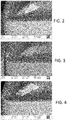
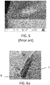
- FIG. 2, FIG. 3, FIG. 4 and FIG. 5 are SEM images of the inserts of Example 1, Example 3, Example 7 and Example 9, respectively. Inserts of Example 1 and 7 in accordance with embodiments of the invention do not show any flaking down to the substrate. Inserts of Example 9 in accordance with prior art show severe flaking along the cutting edge, although having much thinner coating than in Example 1.
- the plasma probe 7 comprises a cylinder of stainless steel connected in one end by a cable and truncated in the other end by an interior sensor element with a circular sensor surface 8 with a diameter of 1 cm and made of stainless steel.
- the sensor surface 8 is isolated from the cylinder and hence collects ions from one direction only.
- a cable in the opposite end of the cylinder connects the cable to an oscilloscope and a power supply.
- the plasma probe 7 was placed in front of the plate-shaped target with the sensor surface 8 facing the plate-shaped target 1 at a distance of about 15cm from the centre of the target surface and the sensor surface 8 was biased at -70 V via the cable. At -70 V the ion current is considered to be saturated and does not vary much with the change in bias voltage. An arc discharge was triggered and the ion current density was measured for different arc currents.
- Example 14a This measurement was performed in a conventional deposition system (Balzers Rapid Coating System) with a ⁇ 16cm Ti 40 Al 60 plate-shaped target using arc currents of 80, 100, 120, 140, 160, 180 and 200A, hereinafter referred to as Example 14a, and in a deposition system with a 74x19cm 2 Ti 40 Al 60 plate-shaped target using arc currents of 100, 200, 300, 400, 500, 600, 700 and 800A, hereinafter referred to as Example 14b.
- the measurements were performed in a nitrogen atmosphere at a pressure of 3.5 Pa and at a temperature of 250 °C and 400 °C, respectively.
- FIG. 6 illustrates the total ion current determined by multiplying the measured ion current density with target size.
- the ion current of the deposition system using the larger plate-shaped targets is significantly larger than in the conventional deposition system.
- the total ion current in the prior art deposition system is 3.3 kA and for an arc current of the deposition system is 8.7kA.
- Thicknesses of the deposited coatings were measured by light optical microscopy on polished cross sections.
- the thickness of the coating on the flank side of the coated cutting tool is larger than on the rake side since the inserts have been mounted with the flank side towards the plate-shaped targets.
- the thickness was measured 0.2 mm from the edge line on each of the flank side and the rake side to reflect this difference.
- the thicknesses given herein refers to the thickness measured on any reasonably flat surface or a surface having a relatively large curvature and some distance away from any edge or corner. For instance, on a drill, the measurements should be performed on the periphery.
- composition of each individual layer can be estimated from the composition of the targets.
- thicker layers have been deposited, thick enough to be analysed, it has been shown that the composition of the deposited layers can differ with a few percentage compared to the composition of the target material. Hence the compositions of the coatings are not given in all of the above examples.
Landscapes
- Chemical & Material Sciences (AREA)
- Engineering & Computer Science (AREA)
- Mechanical Engineering (AREA)
- Materials Engineering (AREA)
- Chemical Kinetics & Catalysis (AREA)
- Metallurgy (AREA)
- Organic Chemistry (AREA)
- Analytical Chemistry (AREA)
- Physics & Mathematics (AREA)
- Plasma & Fusion (AREA)
- Cutting Tools, Boring Holders, And Turrets (AREA)
- Physical Vapour Deposition (AREA)
- Drilling Tools (AREA)
Description
- The present invention relates to a coated cutting tool comprising a substrate and a comparatively thick PVD coating.
- Most cutting tools for turning, milling, drilling or other chip forming machining are today coated with a wear resistant coating deposited using chemical vapor deposition (CVD) or physical vapor deposition (PVD) techniques in order to prolong the service life of the tool and /or to increase the productivity. In general, a comparatively thick coating is aimed for since this improves the wear resistance. This is readily accomplished for CVD coatings. However, PVD coatings have several attractive properties compared to CVD coatings, in particular the ability to provide compressive stress in the coating which gives improved toughness as compared to the CVD coatings. These compressive stresses essentially originate from differences in thermal expansion between substrate and coating and a densification effect due to a bombardment of high energy ions during deposition. This advantageous effect of ion bombardment is hardly present in all PVD techniques such as thermal evaporation but prevails in sputter deposition and with cathodic arc deposition the compressive stress may become excessively high, often greater than 5 GPa, due to high kinetic energy of impinging ions. Biasing of the substrate is a standard way of increasing the kinetic energy and is for hard coatings considered necessary to obtain desired mechanical properties. The densification typically leads to increased hardness and improved wear resistance of the coating material. In combination with a potentially high deposition rate this makes the cathodic arc deposition techniques an interesting alternative for deposition of coatings for cutting tools.
- However, due to too heavy ion bombardment defects may be generated and too high compressive stresses will eventually cause delamination of the coating, spontaneously or due to forces acting on the coating during machining, in particular for thick coatings. Thus, the stress level in the coating is normally controlled to obtain highest possible compressive stress without impairing the adhesion of the coating too much. In particular flaking along the edge of a coated cutting tool insert is a well-known problem. For example,
US 7,838,132 discloses cathodic arc deposition of about 3 µm thick (Ti,Al)N coatings on cemented carbide substrates using an arc current of 200 A at different substrate bias ranging from -40 V to -200 V and concludes that there is an optimum at about -70 V where high compressive stresses, i.e. more than 4 GPa, and still good adhesion can be achieved. Other sophisticated biasing techniques may enable stress relief and bond rearrangement during deposition and thereby allowing a comparatively high kinetic energy without severely suffering from delamination problems. -
US2010/0215912 is concerned with providing hard-coated members having a thick coating having a reduced compression stress, in order to obtain high adhesion and chipping resistance. -
US2010/0260561 discloses coated cutting tools, in which the integrated internal stress at the surface region of the coating is adjusted to a particular range in order to improve the properties of the coating. - Consequently, prior art cathodic arc deposition processes suffer from a trade-off between coating thickness, which is crucial for wear resistance, and quality of the coating with respect to mechanical properties, in particular toughness.
- One object of the invention is to improve wear resistance of coated cutting tools without deteriorating other properties such as flaking resistance. A further object is to provide a PVD coated tool suitable for turning in steel and other applications in which CVD coatings typically are used. This is accomplished by a coated cutting tool as defined by
claim 1. - A coated cutting tool in accordance with the invention comprises a substrate and a coating, where the coating comprises at least one compound layer deposited by cathodic arc deposition and has a thickness of more than 15 µm and up to 30 µm. By thicknesses is for this purpose meant the thickness on the side of the coated cutting tool, i.e. either a flank side or a rake side, which has the thickest coating. The thickness is measured, preferably by light optical microscopy on polished cross sections, about 0.2 mm from the edge line. For irregular surfaces, such as those on e.g. drills and end mills, the thicknesses given herein refers to the thickness measured on any reasonably flat surface or a surface having a relatively large curvature and some distance away from any edge or corner. For instance, on a drill, the measurements should be performed on the periphery. The thickness exceeds coating thicknesses of state-of-the-art coated cutting tools produced by PVD and thereby gives superior crater wear resistance while still performing as good or better with respect to flank wear and flaking. The compound layer comprises Al, and N.
- The compound layer has hard wear resistance, in particular with good abrasive wear resistance.
- The compound layer may be provided in the form of a single layer or a multi-layer structure. By multilayer structure is herein meant a stack of individual layers, at least 5 up to several thousand individual layers, preferably comprising at least two repeatedly alternating individual layers having different properties with respect to e.g. composition. The repetition may be periodic or aperiodic. Contrary to the multi-layer structure the single layer has substantially the same properties throughout the thickness of the single layer. However, one or more properties may be varied continuously in part or throughout the thickness of the single layer, the individual layer of the multi-layer structure or the multi-layer structure. By way of example a compositional gradient may be formed.
- By average composition is herein meant the composition measured on a section of a cross section of the coating. When measured by e.g. Energy-dispersive X-ray Spectroscopy (EDS) on a cross section of the coating the spatial resolution of the measurement may not be enough to resolve the composition of individual layers of a multi-layer structure without contribution from adjacent layers due to low layer thickness. What can readily be measured is the average composition over a section of the multi-layer structure including more than one individual layer.
- In an embodiment of the invention the compound layer is a single layer of Ti1-xAlxN with an average composition of 0.5<x<0.7.
- In another embodiment of the invention the compound layer is a single layer of Ti1-xAlxN with an average composition of 0.3<x<0.5.
- Preferably the substrates of embodiments of the invention are uncoated or coated cutting tools, like cutting tool inserts, round tools such as drills, end mills, taps etc, and is made of any material known to be used in these applications such as cemented carbide, cermets, ceramics, cubic boron nitride, polycrystalline diamond or high-speed steels. More preferably the substrate is made of cemented carbide, cermet or cubic boron nitride since these materials have thermal and mechanical properties that are essential to fully benefit from the advantageous properties of the coating layer deposited on the substrate such that the coated cutting tool obtain excellent wear resistance and toughness.
- A cemented carbide substrate in accordance with one embodiment of the invention preferably comprises 5-13.5 wt-% Co and balance tungsten carbide (WC). Additionally, the elements Ti, Ta, V, Cr, Nb may be present.
- A cemented carbide substrate in accordance with one embodiment of the invention preferably comprises tungsten carbide (WC) with a sub-micron grain size, 5-13,5 wt-% Co, preferably 6-10 wt-% Co, and Cr such that the Cr/Co ratio by weight is 0.04-0.15, and balance WC. Additionally, ppm levels of the elements Ti, Ta, or V. Preferably, the coercivity, He, of this fine-grained substrate ranges from 18-30 kA/m. Preferably the hardness of the substrate, HV3 is from 1500 up to 2200 kgf/mm2, more preferably 1800-2200 kgf/mm2.
- The stress state of the compound layer and thereby the coating of the coated cutting tool in accordance with the invention is preferably controlled by means of deposition parameters and blasting as explained in the following. The blasting has the additional effect that it smoothens the as-deposited coating. The coating has an internal compressive stress ranging from higher than 1.3 to 2 GPa as determined by X-ray diffraction analysis. The surface areal roughness of the coating as measure by white light optical interferometry can be defined by standardized surface texture parameters (ISO 25178). Preferably the surface texture parameter Sa, defining the arithmetical mean height of the surface, is less than 0.4 µm, preferably less than 0.3 µm. In one embodiment of the invention the surface texture is further characterized in that the surface texture parameter Spd, defining the density of peaks, is less than 10x103/mm2. In yet another embodiment of the invention the surface texture is further characterized in that the surface texture parameter Sdr, defining the developed area ratio, is less than 10%, preferably less than 6%.
- The internal stress, σ, of the coating of embodiments of the invention is evaluated by X-ray diffraction measurements using the well-known sin2ψ method as described by I.C. Noyan, J.B. Cohen, Residual Stress Measurement by Diffraction and Interpretation, Springer-Verlag, New York, 1987 (pp 117-130). The measurements shall be performed using CuKα-radiation on the (Ti,Al)N (200) reflection. It is recommended to use the side-inclination technique (ψ-geometry) with six to eleven, preferably eight, ψ-angles, equidistant within a selected sin2ψ-range. An equidistant distribution of Φ-angles within a Φ-sector of 90° is preferred. To confirm a biaxial stress state the sample shall be rotated for Φ=0° and 90° while tilted in ψ. It is recommended to investigate the possible presence of shear stresses and therefore both negative and positive ψ-angles shall be measured. In the case of an Euler 1/4-cradle this is accomplished by measuring the sample also at Φ=180° and 270° for the different ψ-angles. The measurement shall be performed on an as flat surface as possible, preferably on a flank side of an insert. For the calculations of the residual stress values the Possion's ratio, v=0.20 and the Young's modulus, E=450GPa are to be used. Alternatively, Young's modulus, E, can be determined e.g. by nano-indentation technique. Preferably the data are evaluated using commercially available software such as DIFFRACPlus Stress32 v. 1.04 from Bruker AXS preferably locating the (200) reflection by the Pseudo-Voigt-Fit function. In case of a biaxial stress state the total stress is calculated as the average of the obtained biaxial stresses.
- The coating has a compressive stress being higher than 1.3 GPa. By increasing the compressive stress, the toughness can be improved.
- The coating has a compressive stress being lower than 2 GPa. Thanks to this limitation of the compressive stresses in the coating and the advantageous properties of the cathodic arc deposition process a combination of high wear resistance and high flaking resistance can be obtained.
- In one embodiment of the invention the internal stress of the coating is controlled to benefit from the effect of compressive stresses without suffering from delamination problems due to the thickness of the coating. Preferably the thickness of the coating is more than 20 µm.
- In one embodiment of the invention the compound layer of the coating is a single layer of Ti1-XAlXN with an average composition of 0.5<x<0.7, the coating having compressive stress ranging from 1.3GPa to 2GPa. The coating preferably has a predominant (200) texture, i.e. the intensity of (200) is significantly higher than the intensity of (111) as measured by X-ray diffraction. Preferably the surface areal roughness is smooth, i.e. Sa, is less than 0.4 µm, preferably less than 0.3 µm, Spd, is less than 10x103/mm2, and Sdr, is less than 10%, preferably less than 6%. Preferably the substrate is made of cemented carbide, more preferably a fine-grained cemented carbide. This embodiment gives unexpected good result with respect to crater wear, flank wear and flaking. In another embodiment the compound layer is a single layer of Ti1-XAlXN with an average composition of 0.3<x<0.5, otherwise the same properties as the previous embodiment.
- In one embodiment the compound layer comprises a gradient with respect to the internal stress within the coating. This gradient can be determined by control of the deposition conditions and/or the post-treatment blasting. By way of example the bias voltage can be varied during deposition to accomplish an internal stress gradient, by way of example linearly increasing the bias voltage yielding a substantially linear change in internal stress towards higher compressive stress towards the outer surface of the compound layer or the bias voltage can be increased exponentially yielding a steep increase of the internal stress towards higher compressive stress in the outermost part of the compound layer whereas the compressive stress in the inner part of the compound layer is low or even tensile.
- The compound layer may be an innermost layer, closest to the substrate. It may also be an outermost layer of the coating. The coating may comprise of more layers than said at least one compound layer, such as one or more intermediate layers between the substrate and the compound layer or an outermost layer deposited on the compound layer.
- Thanks to the invention it is possible to provide a PVD coated cutting tool insert that outperforms conventional PVD coated cutting tools with respect to crater wear, flank wear without suffering from flaking and that has a crater wear resistance comparable to a state-of-the-art CVD coated cutting tool.
- A method for cathodic arc deposition within a vacuum chamber of a coating comprising at least on compound layer on a substrate in accordance with the invention comprises generating a plasma from an arc discharge visible as one or more arc spots on a surface of a plate-shaped target by applying an arc current of at least 200 A between the plate-shaped target, which acts a cathode, and an anode arrangement such that ions of the arc discharge are emitted out from the plate-shaped target to contribute in forming the coating the substrate.
- It has been found that an ion current density at the surface of the substrate to be coated is of significant importance for the properties of the coating. One measure of the ion current density is the total ion current produced by one or more plate-shaped targets. The total ion current can be estimated by measuring the ion current density with a probe surface negatively biased relative a voltage potential of the anode arrangement and facing the plate-shaped target at a distance of about 15 cm from the target surface and multiplying the measured ion current density with the total surface area of the plate-shaped target. Preferably the total ion current is at least 5 A.
- It has been found that sufficiently high total ion current is not readily accomplished using a small target since the power density of the arc typically becomes be too high to be able to efficiently control the evaporation of target material and hence an unacceptable number of droplets would be emitted from the target surface, which is detrimental to the coating quality. By using a comparatively large target surface area, current density and local thermal load on the target can be kept at moderate levels, while providing the high total ion current.
- The surface area of the plate-shaped target is preferably larger than 500 cm2, more preferably larger than 1000 cm2. Thereby branching of the arc discharge into a multitude of arc spots distributed over substantially the whole surface area of the target is possible. The branching is promoted by the high arc current. One advantage of the branching is that it gives a comparatively uniform ion current density in the plasma over the whole surface area of the target. This can be observed as a substantially uniform illumination of the target surface during deposition. Another advantage of the branching is that it enables improved target utilization. Yet another advantage is that it is possible to obtain uniform deposition conditions in the whole vacuum chamber and hence uniform coating thickness and properties within a batch of substrates to be coated.
- Preferably the measured ion current density, which is measured at saturation conditions of the current, is larger than 6 mA/cm2, more preferably larger than 10 mA/cm2, and even more preferably between 6 mA/cm2 to 16 mA/cm2 in order to obtain the high total ion current and to get a high ion flux at the substrates. Additional plate-shaped targets may be provided, e.g. to further increase ion current supplied to the plasma formed, or to provide plate-shaped targets with different composition.
- The arc discharge supplies ions to the plasma. One measure of the amount of ions that are supplied to the plasma is the total ion current from the plate-shaped target as defined above. With a plurality of plate-shaped targets the supply of ions can be determined by summarizing the total ion current from each of the plate-shaped targets. Preferably the sum of total ion currents from a respective plate-shaped target divided by the volume of the vacuum chamber is at least 3 A/m3.
- The method comprises applying a voltage potential difference between the substrate and the plate-shaped target, i.e. a bias voltage Vs to the substrate being negative relative a voltage potential VA of the anode arrangement and a cathode voltage Vc being negative relative the voltage potential VA of the anode arrangement. As mentioned above, this is known to have an effect on the stress state of the coating, and commonly high bias voltage levels are used to obtain high compressive stresses. However, it has been found that the objectives of the present invention may be accomplished if the substrate is biased at a comparatively low bias level. Preferably voltage differences are
VS-VA>-30 V, -20 V < VC - VA < 0 V, and -10 V < VS - VC ≤10 V. In one example of the method VS - VC ≤ 0 V. In another example -19 V ≤ VC - VA ≤ -15V, preferably -18 V ≤ VC - VA ≤ -16V. In yet another example -30 V ≤ VS - VA ≤ -15 V, preferably -25 V ≤ VS - VA≤ -15 V. For the purpose of this application the bias voltage Vs is intended to be a peak voltage. - Ions impinging on the substrate will due to the comparatively low voltage biasing of the substrate have a moderate kinetic energy, contrary to the above-mentioned prevalent strive to increase the kinetic energy of the ions in order to increase ion mobility and thereby improve mechanical properties. However, due to the high ion current density a high ion flux is provided at the surface of the substrate such that the total energy transferred from ions arriving at the substrate surface is still high thereby enhancing ion mobility at the surface which improves the mechanical properties without introducing detrimental high stress levels and/or defects in the coating. Thereby the stress state in the coating can be efficiently controlled.
- By increasing the arc current the total ion current increases and the deposition rate increases. The increase of the current also promotes branching of the arc discharge. Preferably the arc current that generates the arc plasma is at least 400 A per plate-shaped target, preferably at least 800 A, more preferably 400-1200 A.
- Normally, in prior art cathodic arc deposition systems, chamber walls of the vacuum chamber act as anode for all targets. A deposition system for depositing a coating in accordance the invention preferably comprises an anode arrangement comprising an anode member with an anode surface directed towards the plate-shaped target and arranged concentrically with each plate-shaped target and extending laterally along a rim thereof. The large anode surface is provided close to the target and the anode surface area is fairly constant along the whole length of the plate-shaped target in order to provide uniform plasma conditions along the whole length, irrespective of conditions elsewhere in the vacuum chamber. The anode member is preferably substantially interrupted in a section of the rim extending at least partly along the width of the target on each side of the plate-shaped target in the end portions thereof in order to tailor the shape and size of the anode surface such that the plasma conditions are uniform also in the end portions. The anode member may further comprise an anode surface that tapers outwards as the anode member extends away from the plate-shaped target in the normal direction thereof.
- The anode member of the present invention may further serve to contribute to a balanced electromagnetic field over the whole plate-shaped target. This total electromagnetic field is further influenced by a magnetic self-field originating from the arc current, a magnetic field originating from the means for generating a magnetic field, and a magnetic field originating from current mating of the plate-shaped target. One advantage the balanced electromagnetic field is that the erosion of the plate-shaped targets becomes uniform and the target utilization is improved as compared to conventional deposition systems, in particular for high arc currents above 200 A.
- The deposition system may further comprise means for generating a lateral magnetic field on the target surface. This lateral magnetic field can be used to steer the displacement of the arc spot(s) of the arc plasma. Preferably, the magnetic field originating from means for generating a magnetic field is moderate, preferably less than 100 Gauss, more preferably 5-40 Gauss. This results in a weak steering of the arc discharge, i.e. branches of the arc discharge, around the plate-shaped target.
- The impedance, which is determined by measuring the average voltage and arc current over the anode arrangement and the plate-shaped target, is preferably controlled to be within a predetermined range, preferably less than 0.1 Ohm, more preferably less than 0.05 Ohm, during deposition. This is accomplished at least partly by using a comparatively weak lateral magnetic field for steering the arc discharge, contrary to steered arc techniques where a strong magnetic field is used. These steered arc techniques are conventional ways to slightly increase the arc current, however not readily above 200 A, without impairing the coating properties by increased droplet formation. Likewise, with the anode-cathode configuration described above and the low impedance approach the arc current can be increased to give effective multi-branching of the arc discharge and a dense plasma in order to give a high deposition rate and without impairing coating properties. However, it should be appreciated that the impedance is not only determined by the magnetic field applied, but also other parameters such as anode placement, anode design, gas pressure, cathode design, etc. Therefore, all parameters should be considered when limiting the impedance.
- Weak magnetic steering and well-defined electrical field between anode and cathode improve target utilization since it prevents problems associated with random arc and conventional steered arc techniques. For example, as compared to the latter the typical race track in the target is prevented due to uniform distribution of arc spots and efficient branching of the arc over the target surface.
- By combining the weak magnetic steering with the anode member having a large anode surface close to the target and providing uniform plasma conditions with respect to magnetic field and geometrical arrangement of cathode surface and anode surface around the target, and in particular in the end portions of the plate-shaped target, the anode current density around the target can be kept constant, which enables higher currents and uniform erosion around the target.
- By balancing of the magnetic field with respect to magnetic self-field originating from arc current, magnetic field originating from means for generating a magnetic field, and a magnetic field originating from current mating of the target over the whole surface of the plate-shaped target the erosion of the plate-shaped target transversely to a track around the plate-shaped target is more uniform. Hence, it is possible to improve target utilization.
- The method may further comprise changing the voltage bias gradually during deposition to control the internal stress of the compound layer. Preferably the voltage bias is increased during deposition. The voltage bias may be increased linearly, or progressively, e.g. exponentially.
- Preferably deposition is performed until a thick coating has been formed, at least 15 µm, preferably at least 20 µm. As appreciated by one skilled din the art the deposition process can be varied to accomplish single-layered or multi- layered coatings. Multilayer structures can be accomplished by methods known in the art, by way of example targets of different composition and rotating the substrates to be coated in front of the targets.
- The method may further comprise different pre -treatment or post-treatment steps.
- One example is a pre -treatment comprising subjecting the substrate blasting, preferably a two-step blasting operation including a first dry blasting step to provide an edge rounding of the substrate followed by a second wet blasting step to remove residues from the dry blasting step. However, the blasting can be performed with either dry blasting or wet basting as well. The parameters for pre-treatment blasting can be varied and is well known to a person skilled in the art.
- In another example the coating formed by one or more of the above described steps is subjected to a post-treatment comprising blasting, alternatively shot-peening or the like. In one aspect the blasting may provide a smoother surface. In another aspect the blasting may change the stress state in the coating, e.g. increasing the compressive stresses in the coating. Both aspects may contribute to an improved performance of the coated cutting tool formed by deposition in accordance with embodiment of the invention, in particular for thick coatings. Due to a combination controlling the stress state using the deposition parameters, such as the pressure, the ion current density and the bias, and the post-treatment blasting control of the stress state of the coating can be improved which yields an unexpected good performance of the coated cutting tool.
- Preferably the coating is subjected to wet blasting using a nozzle arranged at a distance of about 20-300 mm, preferably 40-200 mm, and an angle of about 0-90°, preferably 35-65°, relative the rake side of the substrate and 100-800 mesh particles, preferably 300-500 mesh, at a pressure of about 0.1-0.6 MPa. The duration of the wet blasting of the coating is preferably about 0.5-1 minutes. Suitable particles to be used includes, however not limited to, alumina, silicon carbide and zirconia.
- In blasting, a blasting medium, such as particles, are impinging on the substrate with high velocity, typically in an abrasive manner. As mentioned above, the blasting may be performed either under dry conditions, i.e. with the particles or the like as a powder, or wet conditions, i.e. with the particles or the like suspended in a fluid. Depending on the blasting conditions, with respect to blasting medium, pressure, angle and duration, the effect of blasting will vary. The blasting process may for example be adjusted to smoothen or roughen the surface of the substrate. As mentioned above the blasting can also change the stress state of the as-deposited coating. As appreciated by one skilled in the art this change can be tailored by e.g. selecting particular blasting medium, duration, angle, pressure etc.
- As appreciated by one skilled in the art the deposition process may comprises different plasma etching steps, prior to, during or subsequent to deposition of the compound layer or individual layers thereof.
- Other objects, advantages and novel features of the invention will become apparent from the following detailed description of the invention when considered in conjunction with the accompanying drawings and claims.
- Embodiments of the invention will now be described with reference to the accompanying drawings, wherein:
-
FIG. 1 is a schematic illustration of a deposition system for manufacturing a coating in accordance with the invention, -
FIG. 2 is a scanning electron microscope image of a (Ti,Al)N coated cutting tool in accordance with one embodiment of the invention (Example 1) after turning in steel, -
FIG. 3 is a scanning electron microscope image of a (Ti,Al)N coated cutting tool (Example 3) after turning in steel, -
FIG. 4 is a scanning electron microscope image of a (Ti,Al)N coated cutting tool in accordance with one embodiment of the invention (Example 7) after turning in steel, -
FIG. 5 is a scanning electron microscope image of a (Ti,Al)N coated cutting tool in accordance with prior art (Example 9) after turning in steel, -
FIG. 6a is a photograph of the plasma probe used to measure ion current density, -
FIG. 6b illustrates total ion current in front of plate-shaped targets of one embodiment of the invention and of prior art determined from plasma probe measurements. - FIG. la schematically illustrates one example of deposition system for cathodic arc deposition of a coating in accordance with the invention.
Fig. 1b shows front view and top view of a plate-shapedtarget 1 and an anode member. The manufacturing of the coating is herein described with reference to this non-limiting example, however, as appreciated by one skilled in the art, the deposition system can be modified in different ways. As in other PVD depositions systems the deposition of the coating is performed within avacuum chamber 3 coupled to vacuum pumps (not shown) to control the pressure within thevacuum chamber 3. One or more plate-shapedtargets 1 acting as sources of coating material in the deposition process are provided in or on the walls of thevacuum chamber 3 with their target surfaces facing the interior of thevacuum chamber 3. The plate-shapedtargets 1 and an anode arrangement, preferably including theanode member 2, are connected to an arc power supply (not shown) and form cathode and anode of the deposition system, respectively. An arc discharge is used to evaporate target material. The arc discharge is triggered by a trigger (not shown). Asubstrate 5 to be coated is preferably carried by afixture 6 in thevacuum chamber 3 in line-of-sight from the plate-shape targets 1. In order to uniformly coat all sides of thesubstrate 5 the fixture may be rotatable. Thesubstrates 5 may be connected via thefixture 6 to a bias voltage power supply. The deposition may be performed in a reactive atmosphere such that evaporated target material and a reactive gas supplied through a gas inlet into thevacuum chamber 3 react to form a compound coating. - The bias voltage can be provided by a bias voltage power supply. The bias voltage may be a DC voltage or a pulsed voltage. In a deposition system adapted for a pulsed bias voltage the bias voltage power supply comprises a pulse generating unit. The bias voltage power supply is preferably connected to a control unit that monitors the bias voltage output from the bias voltage power supply during deposition and adjusts the power supply to obtain the desired bias voltage level.
- Preferably the arc current is a direct current supplied by a power supply connected to the deposition system. The direct current is not necessarily constant over time. Although the arc current may show considerable variation during deposition due to individual contribution from the short-lived arc discharges, this direct current should not be mixed-up with pulsed deposition techniques. Pulsed deposition can be used for the same reasons as in prior art deposition processes.
- To accomplish impedance control, the deposition system may comprise a control unit and an impedance monitoring unit, arranged such that the control unit based on the measurement of the impedance between the anode and the plate-shaped target by the impedance control unit adjusts the magnitude of the lateral magnetic field generated by means for generating a lateral magnetic field in order to keep the impedance within a predetermined range. The control unit may be automatically or manually controlled.
- Balancing of magnetic self-field originating from arc current, magnetic field originating from means for generating a magnetic field, and a magnetic field originating from current mating of the target is preferably performed by an empirical, iterative process aiming at accomplishing a uniform distribution of the arc spots over the whole surface of the plate-shaped target.
- Balancing of non-uniform magnetic fields originating from the current mating can be accomplished by providing an asymmetric distribution of permanent magnets under the plate-shaped target. By way of example, a cathode arrangement of a deposition system may comprise plate-shaped target arranged on a conductive back plate. The back plate may comprise at least two current bars running along the length thereof. These current bars are connected to the arc power supply in opposite ends of the plate-shaped target and current. Hence the arc current enters the current bars from opposite ends of the plate-shaped target and is spread via the current bars and the conductive back plate to the plate-shaped target. With this configuration the current density in each current bar is higher close to the current input to the current bar and is depleted towards the opposite end. Consequently, the magnetic field originating from the current mating through the current bars is also decreasing along the current bar. The effect of this can be balanced using asymmetrically distributed permanent magnets arranged such that the magnetic field around the plate-shaped target becomes uniform.
- FIG. la schematically illustrates a side view of the anode member used in the following examples.
FIG. 1b schematically illustrates front view and top view of the anode member and the plate-shaped target. The anode member is substantially interrupted in a section extending at least partly along the width of the plate-shaped target in opposite end portions of the plate-shaped target. Further the anode member comprises an anode surface that tapers outwards as the anode member extends away from the plate-shaped target in the normal direction thereof. - In the following, Examples 1, 5, 6 (before blasting) and 7 disclose embodiments of the invention and Examples 8-10 disclose reference samples representing state-of-the-art, which in Examples 11 -13 are compared with respect to crater wear, flank wear and flaking. Examples 2-4 and are provided for information. Substantially the same deposition process has been used for all the samples of Examples 1-7 and is described hereinafter.
- The coatings of Examples 1-7 were deposited on a substrate using a cathodic arc deposition system comprising one or more comparatively large plate-shaped targets as described above. The
substrate 5 to be coated is carried by afixture 6 in line-of-sight from the plate-shape targets 1. In order to uniformly coat all sides of asubstrate 5 the fixture is rotatable. Thesubstrates 5 are connected via thefixture 6 to a bias voltage power supply. The deposition is performed in a reactive atmosphere such that evaporated target material and a reactive gas supplied through a gas inlet into thevacuum chamber 3 react to form a compound coating. - The substrates used in the examples are all CNMG120408 inserts of three different compositions, hereinafter referred to as substrates SI, S2 and S3, respectively. These substrates are specified in Table 1.
Table 1 S1 S2 S3 Co (wt-%) 6.0 7 10 Cr (w(-%) 0.4 0.7 0.4 Ti (wt-%) 0.06 0.01 Ta (wt-%) 0.01 V (wt-%) 0.1 W (wt-%) balance balance balance He (kA/m) 27.6 27.8 20.5 HV3 (kgf/mm2) 1970 1890 1600 - The coercivity value, He, was measured using a Foerster Koerzimat CS1.096 according to DIN IEC 60404-7.
- A (Ti,Al)N coating was deposited on a SI substrate in a nitrogen atmosphere using five plate-shaped targets, each plate-shaped target comprising 40 at-% Ti and 60 at-% Al.
- Prior to loading the substrate into the deposition system, the substrate was subjected to dry blasting to obtain a honing to an edge radius of 30-60 µm followed by wet blasting to clean the substrate from residues from the dry blasting step. The dry blasting was performed using a nozzle with diameter 10 mm arranged at a distance of about 150 mm and an angle of about 45° relative the rake side of the substrate and 100 mesh alumina particles at a pressure of about 0.4-0.6 MPa, i.e. the particles impinging with a 45° angle on the rake side of the substrate. The wet blasting was performed using a nozzle with diameter 9.5 mm arranged at a distance of about 150 mm and an angle of about 45° relative the rake side of the substrate and 360 mesh alumina particles at a pressure of about 0.4 MPa. The duration of the wet blasting of the substrate was about 0.5-1 minutes.
- The substrate was horizontally arranged, i.e. with their flank faces facing the plate-shaped targets, on fixtures enabling threefold rotation in the deposition system. Prior to deposition the substrate was plasma etched by bombarding the substrates with Cr-ions in the deposition system.
- The coating was deposited using the following deposition conditions: temperature 450°C,
nitrogen pressure 5 Pa, arc current 400 A, bias voltage 35.5 V (DC) and cathode voltage 17.5 V. - After deposition the coating was subjected to wet blasting using a nozzle with diameter 9.5 mm arranged at a distance of about 150 mm and an angle of about 45° relative the rake side of the substrate and 360 mesh alumina particles at a pressure of about 0.4 MPa. The duration of the wet blasting of the coating was about 0.5-1 minutes.
- The thickness of the coating was 22 µm on the flank side and 16 µm on the rake side. The hardness was 31 GPa. The internal stress after the wet blasting of the coating was -1430 MPa.
- A (Ti,Al)N coating was deposited on a S2 substrate in a nitrogen atmosphere using five plate-shaped targets, each plate-shaped target comprising 40 at-% Ti and 60 at-% Al.
- Prior to deposition, the substrate was subjected to pre -treatment, horizontally arranged and plasma etched in accordance with Example 1. The coating was deposited using the following deposition conditions: temperature 450 °C,
nitrogen pressure 5 Pa, arc current 400 A, bias voltage 35.5 V (DC) and cathode voltage 17.5 V. After deposition the coating was subjected to post-treatment in accordance with Example 1. - The thickness of the coating was 14µm on the flank side and 8µm on the rake side. The hardness was 31 GPa. The internal stress after wet blasting of the coating was -1950 MPa. Areal surface roughness of the coated cutting tool was measured on the rake side using a white light interferometer (Wyko NT9100, Veeco Instruments Ltd). A Gaussian band-pass filter that rejects wavelengths above 0.08 mm was used for the analysis. The arithmetical mean height of the surface, Sa, was 0.27 µm, the developed area ratio, Sdr, was 5.2%, and the density of peaks, Spd, was 6.1
x10 3 1/mm2. - For comparison a coated cutting tool produced in the same process and with the same substrate as the coated cutting tool of this Example 2, except for being post-treated by blasting was evaluated with respect to the surface areal roughness. The arithmetical mean height of the surface, Sa, was 0.36 µm, the developed area ratio, Sdr, was 24.6%, and the density of peaks, Spd, was 20.9
x10 3 1/mm2. - A (Ti,Al)N coating was deposited on a SI substrate in a nitrogen atmosphere using one plate-shaped target comprising 40 at-% Ti and 60 at-% Al.
- Prior to deposition, the substrate was vertically arranged, i.e. with the rake face facing the plate-shaped target, and thereafter subjected to pre -treatment and plasma etched in accordance with Example 1. The coating was deposited using the following deposition conditions: temperature 450 °C, nitrogen pressure 2.5 Pa, arc current 400 A, bias voltage 19 V (DC) and cathode voltage 17.5 V. After deposition the coating was subjected to wet blasting using a nozzle with diameter 12.5 mm arranged at a distance of 50 mm and an angle of about 45° relative the rake side of the substrate and 500 mesh alumina particles at a pressure of about 0.4 MPa for about 0.5 minutes.
- The thickness of the coating was 21 µm on the flank side and 24µm on the rake side. The hardness was 27 GPa. The internal stress after wet blasting of the coating was +90 MPa.
- A multilayer (Ti,Al,Cr)N coating was deposited on a SI substrate in a nitrogen atmosphere using five plate-shaped targets, each of said five plate-shape targets comprising 40 at-% Ti and 60 at-% Al, running simultaneously with a plate-shaped target comprising 100 at-% Cr .
- Prior to deposition, the substrate was subjected to pre-treatment, horizontally arranged and plasma etched in accordance with Example 1. The coating was deposited using the following deposition conditions: temperature 450 °C, nitrogen pressure 2.5 Pa, arc current for the (Ti,Al) target 400 A, arc current for the Cr target 100 A, bias voltage 19 V (DC) and cathode voltage 17.5 V. After deposition the coating was subjected to post-treatment in accordance with Example 1.
- The thickness of the coating was 16 µm on the flank side and 11 µm on the rake side. The hardness was 31 GPa. The internal stress after wet blasting of the coating was -1340 MPa.
- A TiAIN coating was deposited on a S3 substrate in a nitrogen atmosphere using three plate-shaped targets, each of said three plate-shape targets comprising 60 at-% Ti and 40 at-% Al.
- Prior to loading the substrate into the deposition system, the substrate was subjected to dry blasting to obtain a honing to an edge radius of 30-60 µm followed by wet blasting to clean the substrate from residues from the dry blasting step. The dry blasting was performed using a nozzle with diameter 10 mm arranged at a distance of 150 mm and an angle of 45° relative the rake side of the substrate and 100 mesh alumina particles at a pressure of about 0.4-0.6 MPa. The wet blasting was performed using a nozzle with diameter 12.5 mm arranged at a distance of 50 mm and an angle of about 45° relative the rake side of the substrate and 500 mesh alumina particles at a pressure of about 0.4 MPa for about 0.5 minutes.
- Prior to deposition, the substrate was horizontally arranged and plasma etched in accordance with Example 1. The coating was deposited using the following deposition conditions: temperature 450°C, nitrogen pressure 3.5 Pa, arc current 400 A, bias voltage 20.5 V (pulsed bias, 80% duty cycle) and cathode voltage 17.5 V. After deposition the coating was subjected to post-treatment in accordance with Example 3.
- The thickness of the coating was 23 µm on the flank side and 15 µm on the rake side. The internal stress was +900 MPa after deposition, prior to blasting. The internal stress after blasting of the coating was -1585 MPa. The hardness of the coating was 26 GPa.
- A (Ti,Al)N coating was deposited on a SI substrate in a nitrogen atmosphere using three plate-shaped targets, each of said plate-shape targets comprising 40 at-% Ti and 60 at-% Al.
- Prior to deposition, the substrate was subjected to pre-treatment, horizontally arranged and plasma etched in accordance with Example 1. The coating was deposited using the following deposition conditions: temperature 450 °C, nitrogen pressure 5.0 Pa, arc current 400 A and cathode voltage 17.5 V. During deposition the bias voltage was increased linearly from 20.5 V, at the beginning of deposition, to 36.5 V at the ending of deposition. After deposition the coating was subjected to post-treatment in accordance with Example 1.
- The thickness of the coating was 19 µm on the flank side and 13 µm on the rake side. The internal stress was -1700 MPa after deposition, prior to blasting. The internal stress after wet blasting of the coating was -2580 MPa. Due to this high stress level the coating formed by the above process parameters may spontaneously flake along the cutting edge. This has not been observed for the other Examples of embodiments of the invention since the overall stress level is lower for the coatings thereof. However, a high stress level in the outermost part of the coating can be provided if the stress level in the inner part of the coating is comparatively low, see Example 7. The maximum stress level is also dependent on the thickness of the coating.
- A (Ti,Al)N coating was deposited on a SI substrate in a nitrogen atmosphere using one plate-shaped target, each of said plate-shape targets comprising 40 at-% Ti and 60 at-% Al.
- Prior to deposition, the substrate was subjected to pre -treatment, horizontally arranged and plasma etched in accordance with Example 1. The coating was deposited using the following deposition conditions: temperature 450 °C, nitrogen pressure 5.0 Pa, arc current 400 A and cathode voltage 17.5 V. During deposition the bias voltage was increased exponentially from 20.5 V, at the beginning of deposition, to 36.5 V at the ending of deposition. After deposition the coating was subjected to post-treatment in accordance with Example 1.
- The thickness of the coating was 18 µm on the flank side and 12 µm on the rake side. The internal stress was -965 MPa after deposition, prior to wet blasting of the coating. The internal stress after wet blasting of the coating was -1800MPa.
- A single layer of (Ti,Al)N was deposited on a S2 substrate by cathodic arc deposition in a Balzers Rapid Coating System in a nitrogen atmosphere using targets with the composition Tio.33Alo.67. The thickness of the coating was 3 µm
- A TiAIN multilayer coating with a TiN/(Ti,Al)N multilayer structure repeatedly alternated with a (Ti,Al)N single layer was deposited on a S2 substrate using cathodic arc deposition in a Balzers Rapid Coating System in a nitrogen atmosphere. The TiN/(Ti,Al)N multilayer structure was deposited using Ti and Ti0.5Al0.5 targets and the (Ti,Al)N single layer was deposited using Ti0.5AI0.5 targets. The coating thickness was 4µm.
- A commercial state-of-the-art CVD coated cutting tool for turning applications with a cemented carbide substrate and a MT-TiCN+α-Al2O2TiN coating was used for comparison.
- Inserts from Examples 1-10 were tested with respect to crater wear by turning in bearing steel (Ovako 825B, Tibnor). The result is presented in Table 2. Tool life criterion was crater wear exceeding 0.5 mm2.
Table 2 Example 1 2 3 4 5 6 7 8 9 10 Tool life (min) 20 14 n.a. 10 22 n.a. n.a. 2 10 >30 - Inserts from Examples 1, 2, 4, 5 and 8-10 were tested with respect to flank wear by longitudinal turning in tool steel (Sverker21, Uddeholm). The result is presented in Table 3. Tool life criterion was flank wear exceeding 0.2 mm.
Table 3 Example 1 2 3 4 5 6 7 8 9 10 Tool life (min) 26 28 n.a. 18 12 n.a. n.a. 16 8 12 - Inserts from Examples 1, 3, 4 and 9 were tested with respect to flaking by turning in austenitic stainless steel (304L, Sandvik).
- The extent of flaking was qualitatively determined using a scanning electron microscope (SEM).
FIG. 2, FIG. 3, FIG. 4 andFIG. 5 are SEM images of the inserts of Example 1, Example 3, Example 7 and Example 9, respectively. Inserts of Example 1 and 7 in accordance with embodiments of the invention do not show any flaking down to the substrate. Inserts of Example 9 in accordance with prior art show severe flaking along the cutting edge, although having much thinner coating than in Example 1. - The performance of a coated cutting tool in accordance to the invention with respect to crater wear, flank wear and flaking shown in the above Examples 11-13 makes clear that the coating and the coated cutting tool in accordance with the present invention has excellent toughness and wear resistance. In particular the flaking resistance of such a thick coating is unexpected good.
- In order to evaluate the total ion current generated by a plate-shaped target a plasma probe was used to measure the ion current density in front of a plate -shaped target. As shown in the photograph of
FIG. 5 theplasma probe 7 comprises a cylinder of stainless steel connected in one end by a cable and truncated in the other end by an interior sensor element with acircular sensor surface 8 with a diameter of 1 cm and made of stainless steel. Thesensor surface 8 is isolated from the cylinder and hence collects ions from one direction only. A cable in the opposite end of the cylinder connects the cable to an oscilloscope and a power supply. To perform the measurement theplasma probe 7 was placed in front of the plate-shaped target with thesensor surface 8 facing the plate-shapedtarget 1 at a distance of about 15cm from the centre of the target surface and thesensor surface 8 was biased at -70 V via the cable. At -70 V the ion current is considered to be saturated and does not vary much with the change in bias voltage. An arc discharge was triggered and the ion current density was measured for different arc currents. This measurement was performed in a conventional deposition system (Balzers Rapid Coating System) with a Ø16cm Ti40Al60 plate-shaped target using arc currents of 80, 100, 120, 140, 160, 180 and 200A, hereinafter referred to as Example 14a, and in a deposition system with a 74x19cm2 Ti40Al60 plate-shaped target using arc currents of 100, 200, 300, 400, 500, 600, 700 and 800A, hereinafter referred to as Example 14b. The measurements were performed in a nitrogen atmosphere at a pressure of 3.5 Pa and at a temperature of 250 °C and 400 °C, respectively.FIG. 6 illustrates the total ion current determined by multiplying the measured ion current density with target size. The ion current of the deposition system using the larger plate-shaped targets is significantly larger than in the conventional deposition system. For an arc current of 180A the total ion current in the prior art deposition system is 3.3 kA and for an arc current of the deposition system is 8.7kA. - Thicknesses of the deposited coatings were measured by light optical microscopy on polished cross sections. In general, the thickness of the coating on the flank side of the coated cutting tool is larger than on the rake side since the inserts have been mounted with the flank side towards the plate-shaped targets. Hence the thickness was measured 0.2 mm from the edge line on each of the flank side and the rake side to reflect this difference. For irregular surfaces, such as those on e.g. drills and end mills, the thicknesses given herein refers to the thickness measured on any reasonably flat surface or a surface having a relatively large curvature and some distance away from any edge or corner. For instance, on a drill, the measurements should be performed on the periphery.
- In addition to measurement of composition using EDS or the like the composition of each individual layer can be estimated from the composition of the targets. When thicker layers have been deposited, thick enough to be analysed, it has been shown that the composition of the deposited layers can differ with a few percentage compared to the composition of the target material. Hence the compositions of the coatings are not given in all of the above examples.
- Internal stresses of the coatings were measured on the middle of the flank side of the coated cutting tools, more specifically by X-ray diffraction using ψ-geometry on a X-ray diffractometer Bruker D8 Discover-GADDS equipped with laser-video positioning,
Euler 1/4-cradle, rotating anode as X-ray source (CuKα-radiation) and an area detector (Hi-star). A collimator of size 0.5 mm was used to focus the beam. The analysis was performed on the TiAIN (200) reflection using the goniometer settings 2θ=50°, ω=25° and Φ=0°, 90°, 180°, 270°. Eight ψ tilts ranging from 0° to 70° were performed for each Φ-angle. The sin2Ψ method was used to evaluate the internal stress using the software DIFFRACPlus Stress32 v. 1.04 from Bruker AXS with the constants Young's modulus, E=450 GPa and Poisson's ratio, v=0.20 and locating the reflection using the Pseudo-Voigt-Fit function. - Hardness of the coatings was measured using nano-indentation.
- Terms like in lateral, front, top, in front of, length, width, horizontally etc. are used for illustrative purposes only and are not intended to limit the invention to a specific orientation.
- While the invention has been described in connection with what is presently considered to be the most practical and preferred embodiments, it is to be understood that the invention is not to be limited to the disclosed embodiments, on the contrary, it is intended to cover various modifications and equivalent arrangements within the appended claims.
Claims (12)
- A coated cutting tool comprising a substrate and a coating, where the coating comprises at least one compound layer of Ti1-xAlxN, in which 0.5<x<0.7 or 0.3<x<0.5, which is deposited by cathodic arc deposition, and which has a thickness of more than 15 µm to 30 µm, characterized in that the coating has internal compressive stresses in the range of higher than 1.3 GPa to 2 GPa as determined by X-ray diffraction analysis using the sin2 Ψ method.
- The coated cutting tool of claim 1, wherein the compound layer has a thickness of 20-30 µm.
- The coated cutting tool of any of the preceding claims, wherein the surface areal roughness of the coating with respect to the surface texture parameter Sdr, defining developed area ratio, is less than 10%, preferably less than 6%.
- The coated cutting tool of any of the preceding claims, wherein the surface areal roughness of the coating with respect to the surface texture parameter Spd, defining the density of peaks, is less than 10x103/mm2.
- The coated cutting tool of any of the preceding claims, wherein the surface areal roughness of the coating with respect to the surface texture parameter Sa, defining the arithmetical mean height of the surface, is less than 0.4 µm, preferably less than 0.3.
- The coated cutting tool of any of the preceding layers, wherein the compound layer is a single layer.
- The coated cutting tool of any claims 1-6, wherein the compound layer is a multilayer structure.
- The coated cutting too of any one of the preceding claims, which is post-treated by blasting.
- The coated cutting too of any one of the preceding claims, which comprises a gradient with respect to said internal stress within the coating, with higher compressive stress towards the outer surface of said compound layer.
- The coated cutting tool of any one of the preceding claims, wherein said substrate is a cemented tungsten carbide substrate (WC) with a sub-micron grain size, 5-13,5 wt-% Co, and Cr such that the Cr/Co ratio by weight is 0.04-0.15, balanced WC and ppm levels of the elements Ti, Ta, or V.
- The coated cutting tool of claim 9, wherein the coercivity He of the substrate ranges from 18-30 kA/m.
- The coated cutting tool of claim 9 or 10, wherein the hardness of the substrate HV3 is from 1500 up to 2200 kgf/mm2.
Priority Applications (1)
| Application Number | Priority Date | Filing Date | Title |
|---|---|---|---|
| PL12766413T PL2758561T3 (en) | 2011-09-19 | 2012-09-19 | Coated cutting tool |
Applications Claiming Priority (2)
| Application Number | Priority Date | Filing Date | Title |
|---|---|---|---|
| SE1150851 | 2011-09-19 | ||
| PCT/EP2012/068455 WO2013041576A1 (en) | 2011-09-19 | 2012-09-19 | Coated cutting tool |
Publications (2)
| Publication Number | Publication Date |
|---|---|
| EP2758561A1 EP2758561A1 (en) | 2014-07-30 |
| EP2758561B1 true EP2758561B1 (en) | 2019-04-17 |
Family
ID=46940468
Family Applications (1)
| Application Number | Title | Priority Date | Filing Date |
|---|---|---|---|
| EP12766413.4A Active EP2758561B1 (en) | 2011-09-19 | 2012-09-19 | Coated cutting tool |
Country Status (11)
| Country | Link |
|---|---|
| US (1) | US9399814B2 (en) |
| EP (1) | EP2758561B1 (en) |
| JP (1) | JP6174028B2 (en) |
| KR (1) | KR102095344B1 (en) |
| CN (1) | CN104011256B (en) |
| ES (1) | ES2739283T3 (en) |
| IL (1) | IL231568A0 (en) |
| IN (1) | IN2014DN03070A (en) |
| PL (1) | PL2758561T3 (en) |
| TR (1) | TR201910575T4 (en) |
| WO (1) | WO2013041576A1 (en) |
Families Citing this family (7)
| Publication number | Priority date | Publication date | Assignee | Title |
|---|---|---|---|---|
| CN105177498A (en) * | 2015-05-21 | 2015-12-23 | 广东工业大学 | AlCrSiON nano-composite cutting tool coating and preparation method thereof |
| RU2643536C1 (en) * | 2017-04-04 | 2018-02-02 | федеральное государственное бюджетное образовательное учреждение высшего образования "Ульяновский государственный технический университет" | Method of producing wear-resitant coating for cutting tool |
| CN107299330A (en) * | 2017-04-07 | 2017-10-27 | 苏州星蓝纳米技术有限公司 | A kind of low internal stress coating and preparation method thereof |
| KR102610954B1 (en) | 2017-08-31 | 2023-12-06 | 발터 악티엔게젤샤프트 | Wear-resistant PVD tool coating containing TiAlN nanolayer films |
| CN110408893A (en) * | 2019-07-12 | 2019-11-05 | 厦门金鹭特种合金有限公司 | A kind of PVD coated carbides cutting tip and preparation method thereof |
| WO2022097286A1 (en) * | 2020-11-06 | 2022-05-12 | 貴嗣 飯塚 | Film formation apparatus, film formation unit and film formation method |
| CN112746246B (en) * | 2020-12-11 | 2022-06-24 | 广东工业大学 | Method for preparing nitride composite coating based on arc ion plating high flux |
Family Cites Families (29)
| Publication number | Priority date | Publication date | Assignee | Title |
|---|---|---|---|---|
| DE19547305A1 (en) * | 1995-12-18 | 1997-06-19 | Univ Sheffield | Coating metal substrates with titanium aluminium nitride for coating steel |
| WO1998010120A1 (en) * | 1996-09-03 | 1998-03-12 | Balzers Aktiengesellschaft | Workpiece with wear-protective coating |
| JP2000080466A (en) | 1998-09-01 | 2000-03-21 | Kobe Steel Ltd | Vacuum arc deposition device |
| IL140024A0 (en) * | 1999-12-03 | 2002-02-10 | Sumitomo Electric Industries | Coated pcbn cutting tools |
| JP2001322005A (en) | 2000-05-12 | 2001-11-20 | Mitsubishi Materials Corp | Surface coated cemented carbide cutting tool with excellent wear resistance |
| JP4112836B2 (en) * | 2001-06-19 | 2008-07-02 | 株式会社神戸製鋼所 | Target for forming hard coatings for cutting tools |
| ATE441737T1 (en) * | 2000-12-28 | 2009-09-15 | Kobe Steel Ltd | TARGET FOR FORMING A HARD LAYER |
| JP2002346812A (en) * | 2001-05-25 | 2002-12-04 | Ngk Spark Plug Co Ltd | Cutting tool and tool with holder |
| SE526339C2 (en) * | 2002-09-04 | 2005-08-23 | Seco Tools Ab | Cut with durable refractory coating with composite structure |
| JP2006028600A (en) * | 2004-07-16 | 2006-02-02 | Kobe Steel Ltd | Stacked film having excellent wear resistance and heat resistance |
| SE528789C2 (en) | 2004-09-10 | 2007-02-13 | Sandvik Intellectual Property | PVD-coated cemented carbide cutter and way to manufacture it |
| SE530516C2 (en) * | 2006-06-15 | 2008-06-24 | Sandvik Intellectual Property | Coated cemented carbide insert, method of making this and its use in milling cast iron |
| SE530735C2 (en) * | 2006-10-18 | 2008-08-26 | Sandvik Intellectual Property | A coated carbide cutter, especially useful for turning steel |
| SE0700800L (en) | 2006-12-15 | 2008-06-16 | Sandvik Intellectual Property | Coated cutting tool |
| DE102007015587A1 (en) | 2007-03-29 | 2008-10-02 | Gühring Ohg | Anti-wear coating for rotating cutting tools, e.g. drills, comprises nitrides of chromium, titanium and aluminum, coating being made smoother by reducing the number of microdroplets in it |
| US8455116B2 (en) * | 2007-06-01 | 2013-06-04 | Sandvik Intellectual Property Ab | Coated cemented carbide cutting tool insert |
| SE0701761A0 (en) * | 2007-06-01 | 2008-12-02 | Sandvik Intellectual Property | Fine-grained cemented carbide for turning in hot-strength super alloys (HRSA) and stainless steel |
| WO2009002266A1 (en) * | 2007-06-27 | 2008-12-31 | Sandvik Intellectual Property Ab | Coated cemented carbide inserts for milling of especially hard cast steel |
| SE531971C2 (en) * | 2007-08-24 | 2009-09-15 | Seco Tools Ab | Coated cutting tool for general turning in hot-strength super alloys (HRSA) |
| WO2009047867A1 (en) * | 2007-10-12 | 2009-04-16 | Hitachi Tool Engineering, Ltd. | Member covered with hard coating film and process for the production of the member |
| DE102008019202A1 (en) * | 2008-04-17 | 2009-10-22 | Kennametal Inc. | Coating method, workpiece or tool and its use |
| JP5231859B2 (en) * | 2008-04-30 | 2013-07-10 | 住友電気工業株式会社 | Surface coated cutting tool |
| KR101255430B1 (en) * | 2008-04-30 | 2013-04-17 | 스미또모 덴꼬오 하드메탈 가부시끼가이샤 | Surface coated cutting tool |
| US8216702B2 (en) * | 2008-06-13 | 2012-07-10 | Seco Tools Ab | Coated cutting tool for metal cutting applications generating high temperatures |
| WO2010002344A1 (en) * | 2008-07-01 | 2010-01-07 | Sandvik Intellectual Property Ab | A cemented carbide insert for turning |
| JP4964268B2 (en) * | 2009-04-10 | 2012-06-27 | 住友電気工業株式会社 | Surface coated cutting tool |
| EP2392688A1 (en) * | 2010-06-07 | 2011-12-07 | Sandvik Intellectual Property AB | Coated cutting tool |
| KR101430324B1 (en) * | 2010-10-28 | 2014-08-13 | 스미또모 덴꼬오 하드메탈 가부시끼가이샤 | Surface-coated sintered compact |
| US8409702B2 (en) * | 2011-02-07 | 2013-04-02 | Kennametal Inc. | Cubic aluminum titanium nitride coating and method of making same |
-
2012
- 2012-09-19 IN IN3070DEN2014 patent/IN2014DN03070A/en unknown
- 2012-09-19 EP EP12766413.4A patent/EP2758561B1/en active Active
- 2012-09-19 WO PCT/EP2012/068455 patent/WO2013041576A1/en active Application Filing
- 2012-09-19 US US14/345,532 patent/US9399814B2/en not_active Expired - Fee Related
- 2012-09-19 TR TR2019/10575T patent/TR201910575T4/en unknown
- 2012-09-19 CN CN201280050674.1A patent/CN104011256B/en not_active Expired - Fee Related
- 2012-09-19 KR KR1020147010184A patent/KR102095344B1/en active IP Right Grant
- 2012-09-19 ES ES12766413T patent/ES2739283T3/en active Active
- 2012-09-19 PL PL12766413T patent/PL2758561T3/en unknown
- 2012-09-19 JP JP2014530280A patent/JP6174028B2/en not_active Expired - Fee Related
-
2014
- 2014-03-18 IL IL231568A patent/IL231568A0/en active IP Right Grant
Non-Patent Citations (1)
| Title |
|---|
| None * |
Also Published As
| Publication number | Publication date |
|---|---|
| WO2013041576A1 (en) | 2013-03-28 |
| CN104011256B (en) | 2016-10-26 |
| JP6174028B2 (en) | 2017-08-02 |
| ES2739283T3 (en) | 2020-01-30 |
| CN104011256A (en) | 2014-08-27 |
| KR20140065447A (en) | 2014-05-29 |
| JP2014526393A (en) | 2014-10-06 |
| IL231568A0 (en) | 2014-04-30 |
| US20140377023A1 (en) | 2014-12-25 |
| TR201910575T4 (en) | 2019-08-21 |
| IN2014DN03070A (en) | 2015-05-15 |
| US9399814B2 (en) | 2016-07-26 |
| PL2758561T3 (en) | 2019-11-29 |
| EP2758561A1 (en) | 2014-07-30 |
| KR102095344B1 (en) | 2020-04-01 |
Similar Documents
| Publication | Publication Date | Title |
|---|---|---|
| EP2758561B1 (en) | Coated cutting tool | |
| EP3269479B1 (en) | Surface-coated cutting tool and method for manufacturing same | |
| CN107636190B (en) | Cutting tool with multilayer arc PVD coating | |
| US7838132B2 (en) | PVD-coated cutting tool insert | |
| EP3715026B1 (en) | Coated cutting tool | |
| KR20160136324A (en) | Surface-coated cutting tool and production method therefor | |
| KR20150045425A (en) | Surface-coated cutting tool | |
| CN107278177B (en) | Whole hard alloy end mill(ing) cutter with TiAlN-ZrN coating | |
| CN114846176B (en) | Coated cutting tool | |
| EP4292735A1 (en) | Coated tool | |
| JP2011152602A (en) | Surface-coated cutting tool provided with hard coated layer demonstrating superior chipping resistance | |
| US9587305B2 (en) | Cathodic arc deposition | |
| EP4108366A1 (en) | Coated tool | |
| EP4389329A1 (en) | Coated tool | |
| US11033969B2 (en) | Cutting tool | |
| JP5585929B2 (en) | Surface-coated cutting tool with excellent fracture resistance due to hard coating layer |
Legal Events
| Date | Code | Title | Description |
|---|---|---|---|
| PUAI | Public reference made under article 153(3) epc to a published international application that has entered the european phase |
Free format text: ORIGINAL CODE: 0009012 |
|
| 17P | Request for examination filed |
Effective date: 20140416 |
|
| AK | Designated contracting states |
Kind code of ref document: A1 Designated state(s): AL AT BE BG CH CY CZ DE DK EE ES FI FR GB GR HR HU IE IS IT LI LT LU LV MC MK MT NL NO PL PT RO RS SE SI SK SM TR |
|
| DAX | Request for extension of the european patent (deleted) | ||
| STAA | Information on the status of an ep patent application or granted ep patent |
Free format text: STATUS: EXAMINATION IS IN PROGRESS |
|
| 17Q | First examination report despatched |
Effective date: 20180309 |
|
| GRAP | Despatch of communication of intention to grant a patent |
Free format text: ORIGINAL CODE: EPIDOSNIGR1 |
|
| STAA | Information on the status of an ep patent application or granted ep patent |
Free format text: STATUS: GRANT OF PATENT IS INTENDED |
|
| RIC1 | Information provided on ipc code assigned before grant |
Ipc: H01J 37/32 20060101ALI20181012BHEP Ipc: C23C 14/58 20060101ALI20181012BHEP Ipc: C23C 14/06 20060101ALI20181012BHEP Ipc: C23C 14/32 20060101AFI20181012BHEP Ipc: B23B 27/14 20060101ALI20181012BHEP |
|
| INTG | Intention to grant announced |
Effective date: 20181031 |
|
| GRAS | Grant fee paid |
Free format text: ORIGINAL CODE: EPIDOSNIGR3 |
|
| GRAA | (expected) grant |
Free format text: ORIGINAL CODE: 0009210 |
|
| STAA | Information on the status of an ep patent application or granted ep patent |
Free format text: STATUS: THE PATENT HAS BEEN GRANTED |
|
| AK | Designated contracting states |
Kind code of ref document: B1 Designated state(s): AL AT BE BG CH CY CZ DE DK EE ES FI FR GB GR HR HU IE IS IT LI LT LU LV MC MK MT NL NO PL PT RO RS SE SI SK SM TR |
|
| REG | Reference to a national code |
Ref country code: GB Ref legal event code: FG4D |
|
| REG | Reference to a national code |
Ref country code: CH Ref legal event code: EP |
|
| REG | Reference to a national code |
Ref country code: DE Ref legal event code: R096 Ref document number: 602012059096 Country of ref document: DE |
|
| REG | Reference to a national code |
Ref country code: AT Ref legal event code: REF Ref document number: 1121635 Country of ref document: AT Kind code of ref document: T Effective date: 20190515 Ref country code: IE Ref legal event code: FG4D |
|
| REG | Reference to a national code |
Ref country code: SE Ref legal event code: TRGR |
|
| REG | Reference to a national code |
Ref country code: CH Ref legal event code: NV Representative=s name: OMNIS-IP SA, CH |
|
| REG | Reference to a national code |
Ref country code: NL Ref legal event code: MP Effective date: 20190417 |
|
| REG | Reference to a national code |
Ref country code: LT Ref legal event code: MG4D |
|
| PG25 | Lapsed in a contracting state [announced via postgrant information from national office to epo] |
Ref country code: NL Free format text: LAPSE BECAUSE OF FAILURE TO SUBMIT A TRANSLATION OF THE DESCRIPTION OR TO PAY THE FEE WITHIN THE PRESCRIBED TIME-LIMIT Effective date: 20190417 |
|
| PG25 | Lapsed in a contracting state [announced via postgrant information from national office to epo] |
Ref country code: AL Free format text: LAPSE BECAUSE OF FAILURE TO SUBMIT A TRANSLATION OF THE DESCRIPTION OR TO PAY THE FEE WITHIN THE PRESCRIBED TIME-LIMIT Effective date: 20190417 Ref country code: PT Free format text: LAPSE BECAUSE OF FAILURE TO SUBMIT A TRANSLATION OF THE DESCRIPTION OR TO PAY THE FEE WITHIN THE PRESCRIBED TIME-LIMIT Effective date: 20190817 Ref country code: HR Free format text: LAPSE BECAUSE OF FAILURE TO SUBMIT A TRANSLATION OF THE DESCRIPTION OR TO PAY THE FEE WITHIN THE PRESCRIBED TIME-LIMIT Effective date: 20190417 Ref country code: LT Free format text: LAPSE BECAUSE OF FAILURE TO SUBMIT A TRANSLATION OF THE DESCRIPTION OR TO PAY THE FEE WITHIN THE PRESCRIBED TIME-LIMIT Effective date: 20190417 Ref country code: NO Free format text: LAPSE BECAUSE OF FAILURE TO SUBMIT A TRANSLATION OF THE DESCRIPTION OR TO PAY THE FEE WITHIN THE PRESCRIBED TIME-LIMIT Effective date: 20190717 Ref country code: FI Free format text: LAPSE BECAUSE OF FAILURE TO SUBMIT A TRANSLATION OF THE DESCRIPTION OR TO PAY THE FEE WITHIN THE PRESCRIBED TIME-LIMIT Effective date: 20190417 |
|
| PG25 | Lapsed in a contracting state [announced via postgrant information from national office to epo] |
Ref country code: LV Free format text: LAPSE BECAUSE OF FAILURE TO SUBMIT A TRANSLATION OF THE DESCRIPTION OR TO PAY THE FEE WITHIN THE PRESCRIBED TIME-LIMIT Effective date: 20190417 Ref country code: RS Free format text: LAPSE BECAUSE OF FAILURE TO SUBMIT A TRANSLATION OF THE DESCRIPTION OR TO PAY THE FEE WITHIN THE PRESCRIBED TIME-LIMIT Effective date: 20190417 Ref country code: BG Free format text: LAPSE BECAUSE OF FAILURE TO SUBMIT A TRANSLATION OF THE DESCRIPTION OR TO PAY THE FEE WITHIN THE PRESCRIBED TIME-LIMIT Effective date: 20190717 Ref country code: GR Free format text: LAPSE BECAUSE OF FAILURE TO SUBMIT A TRANSLATION OF THE DESCRIPTION OR TO PAY THE FEE WITHIN THE PRESCRIBED TIME-LIMIT Effective date: 20190718 |
|
| PG25 | Lapsed in a contracting state [announced via postgrant information from national office to epo] |
Ref country code: IS Free format text: LAPSE BECAUSE OF FAILURE TO SUBMIT A TRANSLATION OF THE DESCRIPTION OR TO PAY THE FEE WITHIN THE PRESCRIBED TIME-LIMIT Effective date: 20190817 |
|
| REG | Reference to a national code |
Ref country code: DE Ref legal event code: R097 Ref document number: 602012059096 Country of ref document: DE |
|
| REG | Reference to a national code |
Ref country code: ES Ref legal event code: FG2A Ref document number: 2739283 Country of ref document: ES Kind code of ref document: T3 Effective date: 20200130 |
|
| PG25 | Lapsed in a contracting state [announced via postgrant information from national office to epo] |
Ref country code: DK Free format text: LAPSE BECAUSE OF FAILURE TO SUBMIT A TRANSLATION OF THE DESCRIPTION OR TO PAY THE FEE WITHIN THE PRESCRIBED TIME-LIMIT Effective date: 20190417 Ref country code: SK Free format text: LAPSE BECAUSE OF FAILURE TO SUBMIT A TRANSLATION OF THE DESCRIPTION OR TO PAY THE FEE WITHIN THE PRESCRIBED TIME-LIMIT Effective date: 20190417 Ref country code: EE Free format text: LAPSE BECAUSE OF FAILURE TO SUBMIT A TRANSLATION OF THE DESCRIPTION OR TO PAY THE FEE WITHIN THE PRESCRIBED TIME-LIMIT Effective date: 20190417 Ref country code: RO Free format text: LAPSE BECAUSE OF FAILURE TO SUBMIT A TRANSLATION OF THE DESCRIPTION OR TO PAY THE FEE WITHIN THE PRESCRIBED TIME-LIMIT Effective date: 20190417 |
|
| PLBE | No opposition filed within time limit |
Free format text: ORIGINAL CODE: 0009261 |
|
| STAA | Information on the status of an ep patent application or granted ep patent |
Free format text: STATUS: NO OPPOSITION FILED WITHIN TIME LIMIT |
|
| PG25 | Lapsed in a contracting state [announced via postgrant information from national office to epo] |
Ref country code: SM Free format text: LAPSE BECAUSE OF FAILURE TO SUBMIT A TRANSLATION OF THE DESCRIPTION OR TO PAY THE FEE WITHIN THE PRESCRIBED TIME-LIMIT Effective date: 20190417 |
|
| 26N | No opposition filed |
Effective date: 20200120 |
|
| PG25 | Lapsed in a contracting state [announced via postgrant information from national office to epo] |
Ref country code: MC Free format text: LAPSE BECAUSE OF FAILURE TO SUBMIT A TRANSLATION OF THE DESCRIPTION OR TO PAY THE FEE WITHIN THE PRESCRIBED TIME-LIMIT Effective date: 20190417 Ref country code: SI Free format text: LAPSE BECAUSE OF FAILURE TO SUBMIT A TRANSLATION OF THE DESCRIPTION OR TO PAY THE FEE WITHIN THE PRESCRIBED TIME-LIMIT Effective date: 20190417 |
|
| PG25 | Lapsed in a contracting state [announced via postgrant information from national office to epo] |
Ref country code: IE Free format text: LAPSE BECAUSE OF NON-PAYMENT OF DUE FEES Effective date: 20190919 |
|
| REG | Reference to a national code |
Ref country code: BE Ref legal event code: MM Effective date: 20190930 |
|
| PG25 | Lapsed in a contracting state [announced via postgrant information from national office to epo] |
Ref country code: BE Free format text: LAPSE BECAUSE OF NON-PAYMENT OF DUE FEES Effective date: 20190930 |
|
| PGFP | Annual fee paid to national office [announced via postgrant information from national office to epo] |
Ref country code: CZ Payment date: 20200918 Year of fee payment: 9 Ref country code: DE Payment date: 20200925 Year of fee payment: 9 Ref country code: FR Payment date: 20200914 Year of fee payment: 9 Ref country code: TR Payment date: 20200917 Year of fee payment: 9 Ref country code: LU Payment date: 20200923 Year of fee payment: 9 Ref country code: GB Payment date: 20200922 Year of fee payment: 9 |
|
| PGFP | Annual fee paid to national office [announced via postgrant information from national office to epo] |
Ref country code: SE Payment date: 20200925 Year of fee payment: 9 Ref country code: IT Payment date: 20200922 Year of fee payment: 9 Ref country code: CH Payment date: 20200921 Year of fee payment: 9 Ref country code: AT Payment date: 20200921 Year of fee payment: 9 |
|
| PGFP | Annual fee paid to national office [announced via postgrant information from national office to epo] |
Ref country code: ES Payment date: 20201120 Year of fee payment: 9 |
|
| PG25 | Lapsed in a contracting state [announced via postgrant information from national office to epo] |
Ref country code: CY Free format text: LAPSE BECAUSE OF FAILURE TO SUBMIT A TRANSLATION OF THE DESCRIPTION OR TO PAY THE FEE WITHIN THE PRESCRIBED TIME-LIMIT Effective date: 20190417 |
|
| PG25 | Lapsed in a contracting state [announced via postgrant information from national office to epo] |
Ref country code: HU Free format text: LAPSE BECAUSE OF FAILURE TO SUBMIT A TRANSLATION OF THE DESCRIPTION OR TO PAY THE FEE WITHIN THE PRESCRIBED TIME-LIMIT; INVALID AB INITIO Effective date: 20120919 Ref country code: MT Free format text: LAPSE BECAUSE OF FAILURE TO SUBMIT A TRANSLATION OF THE DESCRIPTION OR TO PAY THE FEE WITHIN THE PRESCRIBED TIME-LIMIT Effective date: 20190417 |
|
| REG | Reference to a national code |
Ref country code: DE Ref legal event code: R119 Ref document number: 602012059096 Country of ref document: DE |
|
| REG | Reference to a national code |
Ref country code: SE Ref legal event code: EUG |
|
| REG | Reference to a national code |
Ref country code: CH Ref legal event code: PL |
|
| REG | Reference to a national code |
Ref country code: AT Ref legal event code: MM01 Ref document number: 1121635 Country of ref document: AT Kind code of ref document: T Effective date: 20210919 |
|
| GBPC | Gb: european patent ceased through non-payment of renewal fee |
Effective date: 20210919 |
|
| PG25 | Lapsed in a contracting state [announced via postgrant information from national office to epo] |
Ref country code: CZ Free format text: LAPSE BECAUSE OF NON-PAYMENT OF DUE FEES Effective date: 20210919 |
|
| PG25 | Lapsed in a contracting state [announced via postgrant information from national office to epo] |
Ref country code: MK Free format text: LAPSE BECAUSE OF FAILURE TO SUBMIT A TRANSLATION OF THE DESCRIPTION OR TO PAY THE FEE WITHIN THE PRESCRIBED TIME-LIMIT Effective date: 20190417 |
|
| PG25 | Lapsed in a contracting state [announced via postgrant information from national office to epo] |
Ref country code: SE Free format text: LAPSE BECAUSE OF NON-PAYMENT OF DUE FEES Effective date: 20210920 Ref country code: LU Free format text: LAPSE BECAUSE OF NON-PAYMENT OF DUE FEES Effective date: 20210919 Ref country code: GB Free format text: LAPSE BECAUSE OF NON-PAYMENT OF DUE FEES Effective date: 20210919 Ref country code: FR Free format text: LAPSE BECAUSE OF NON-PAYMENT OF DUE FEES Effective date: 20210930 Ref country code: DE Free format text: LAPSE BECAUSE OF NON-PAYMENT OF DUE FEES Effective date: 20220401 |
|
| PG25 | Lapsed in a contracting state [announced via postgrant information from national office to epo] |
Ref country code: LI Free format text: LAPSE BECAUSE OF NON-PAYMENT OF DUE FEES Effective date: 20210930 Ref country code: CH Free format text: LAPSE BECAUSE OF NON-PAYMENT OF DUE FEES Effective date: 20210930 Ref country code: AT Free format text: LAPSE BECAUSE OF NON-PAYMENT OF DUE FEES Effective date: 20210919 |
|
| REG | Reference to a national code |
Ref country code: AT Ref legal event code: UEP Ref document number: 1121635 Country of ref document: AT Kind code of ref document: T Effective date: 20190417 |
|
| PG25 | Lapsed in a contracting state [announced via postgrant information from national office to epo] |
Ref country code: IT Free format text: LAPSE BECAUSE OF NON-PAYMENT OF DUE FEES Effective date: 20210919 |
|
| REG | Reference to a national code |
Ref country code: ES Ref legal event code: FD2A Effective date: 20221125 |
|
| PG25 | Lapsed in a contracting state [announced via postgrant information from national office to epo] |
Ref country code: ES Free format text: LAPSE BECAUSE OF NON-PAYMENT OF DUE FEES Effective date: 20210920 |
|
| PGFP | Annual fee paid to national office [announced via postgrant information from national office to epo] |
Ref country code: PL Payment date: 20200820 Year of fee payment: 9 |
|
| PG25 | Lapsed in a contracting state [announced via postgrant information from national office to epo] |
Ref country code: PL Free format text: LAPSE BECAUSE OF NON-PAYMENT OF DUE FEES Effective date: 20210919 |
|
| PG25 | Lapsed in a contracting state [announced via postgrant information from national office to epo] |
Ref country code: PL Free format text: LAPSE BECAUSE OF NON-PAYMENT OF DUE FEES Effective date: 20210919 |