EP2754738A1 - Substrate for epitaxial growth, and crystal laminate structure - Google Patents
Substrate for epitaxial growth, and crystal laminate structure Download PDFInfo
- Publication number
- EP2754738A1 EP2754738A1 EP12830660.2A EP12830660A EP2754738A1 EP 2754738 A1 EP2754738 A1 EP 2754738A1 EP 12830660 A EP12830660 A EP 12830660A EP 2754738 A1 EP2754738 A1 EP 2754738A1
- Authority
- EP
- European Patent Office
- Prior art keywords
- crystal
- plane
- epitaxial growth
- growth substrate
- layer
- Prior art date
- Legal status (The legal status is an assumption and is not a legal conclusion. Google has not performed a legal analysis and makes no representation as to the accuracy of the status listed.)
- Granted
Links
Images





Classifications
-
- H—ELECTRICITY
- H10—SEMICONDUCTOR DEVICES; ELECTRIC SOLID-STATE DEVICES NOT OTHERWISE PROVIDED FOR
- H10D—INORGANIC ELECTRIC SEMICONDUCTOR DEVICES
- H10D62/00—Semiconductor bodies, or regions thereof, of devices having potential barriers
- H10D62/80—Semiconductor bodies, or regions thereof, of devices having potential barriers characterised by the materials
-
- C—CHEMISTRY; METALLURGY
- C30—CRYSTAL GROWTH
- C30B—SINGLE-CRYSTAL GROWTH; UNIDIRECTIONAL SOLIDIFICATION OF EUTECTIC MATERIAL OR UNIDIRECTIONAL DEMIXING OF EUTECTOID MATERIAL; REFINING BY ZONE-MELTING OF MATERIAL; PRODUCTION OF A HOMOGENEOUS POLYCRYSTALLINE MATERIAL WITH DEFINED STRUCTURE; SINGLE CRYSTALS OR HOMOGENEOUS POLYCRYSTALLINE MATERIAL WITH DEFINED STRUCTURE; AFTER-TREATMENT OF SINGLE CRYSTALS OR A HOMOGENEOUS POLYCRYSTALLINE MATERIAL WITH DEFINED STRUCTURE; APPARATUS THEREFOR
- C30B29/00—Single crystals or homogeneous polycrystalline material with defined structure characterised by the material or by their shape
- C30B29/10—Inorganic compounds or compositions
- C30B29/16—Oxides
-
- C—CHEMISTRY; METALLURGY
- C30—CRYSTAL GROWTH
- C30B—SINGLE-CRYSTAL GROWTH; UNIDIRECTIONAL SOLIDIFICATION OF EUTECTIC MATERIAL OR UNIDIRECTIONAL DEMIXING OF EUTECTOID MATERIAL; REFINING BY ZONE-MELTING OF MATERIAL; PRODUCTION OF A HOMOGENEOUS POLYCRYSTALLINE MATERIAL WITH DEFINED STRUCTURE; SINGLE CRYSTALS OR HOMOGENEOUS POLYCRYSTALLINE MATERIAL WITH DEFINED STRUCTURE; AFTER-TREATMENT OF SINGLE CRYSTALS OR A HOMOGENEOUS POLYCRYSTALLINE MATERIAL WITH DEFINED STRUCTURE; APPARATUS THEREFOR
- C30B23/00—Single-crystal growth by condensing evaporated or sublimed materials
- C30B23/02—Epitaxial-layer growth
- C30B23/06—Heating of the deposition chamber, the substrate or the materials to be evaporated
- C30B23/066—Heating of the material to be evaporated
-
- C—CHEMISTRY; METALLURGY
- C30—CRYSTAL GROWTH
- C30B—SINGLE-CRYSTAL GROWTH; UNIDIRECTIONAL SOLIDIFICATION OF EUTECTIC MATERIAL OR UNIDIRECTIONAL DEMIXING OF EUTECTOID MATERIAL; REFINING BY ZONE-MELTING OF MATERIAL; PRODUCTION OF A HOMOGENEOUS POLYCRYSTALLINE MATERIAL WITH DEFINED STRUCTURE; SINGLE CRYSTALS OR HOMOGENEOUS POLYCRYSTALLINE MATERIAL WITH DEFINED STRUCTURE; AFTER-TREATMENT OF SINGLE CRYSTALS OR A HOMOGENEOUS POLYCRYSTALLINE MATERIAL WITH DEFINED STRUCTURE; APPARATUS THEREFOR
- C30B29/00—Single crystals or homogeneous polycrystalline material with defined structure characterised by the material or by their shape
- C30B29/10—Inorganic compounds or compositions
- C30B29/16—Oxides
- C30B29/22—Complex oxides
-
- C—CHEMISTRY; METALLURGY
- C30—CRYSTAL GROWTH
- C30B—SINGLE-CRYSTAL GROWTH; UNIDIRECTIONAL SOLIDIFICATION OF EUTECTIC MATERIAL OR UNIDIRECTIONAL DEMIXING OF EUTECTOID MATERIAL; REFINING BY ZONE-MELTING OF MATERIAL; PRODUCTION OF A HOMOGENEOUS POLYCRYSTALLINE MATERIAL WITH DEFINED STRUCTURE; SINGLE CRYSTALS OR HOMOGENEOUS POLYCRYSTALLINE MATERIAL WITH DEFINED STRUCTURE; AFTER-TREATMENT OF SINGLE CRYSTALS OR A HOMOGENEOUS POLYCRYSTALLINE MATERIAL WITH DEFINED STRUCTURE; APPARATUS THEREFOR
- C30B29/00—Single crystals or homogeneous polycrystalline material with defined structure characterised by the material or by their shape
- C30B29/60—Single crystals or homogeneous polycrystalline material with defined structure characterised by the material or by their shape characterised by shape
- C30B29/68—Crystals with laminate structure, e.g. "superlattices"
-
- H—ELECTRICITY
- H10—SEMICONDUCTOR DEVICES; ELECTRIC SOLID-STATE DEVICES NOT OTHERWISE PROVIDED FOR
- H10D—INORGANIC ELECTRIC SEMICONDUCTOR DEVICES
- H10D62/00—Semiconductor bodies, or regions thereof, of devices having potential barriers
- H10D62/40—Crystalline structures
-
- H—ELECTRICITY
- H10—SEMICONDUCTOR DEVICES; ELECTRIC SOLID-STATE DEVICES NOT OTHERWISE PROVIDED FOR
- H10D—INORGANIC ELECTRIC SEMICONDUCTOR DEVICES
- H10D62/00—Semiconductor bodies, or regions thereof, of devices having potential barriers
- H10D62/40—Crystalline structures
- H10D62/405—Orientations of crystalline planes
-
- H—ELECTRICITY
- H10—SEMICONDUCTOR DEVICES; ELECTRIC SOLID-STATE DEVICES NOT OTHERWISE PROVIDED FOR
- H10P—GENERIC PROCESSES OR APPARATUS FOR THE MANUFACTURE OR TREATMENT OF DEVICES COVERED BY CLASS H10
- H10P14/00—Formation of materials, e.g. in the shape of layers or pillars
- H10P14/20—Formation of materials, e.g. in the shape of layers or pillars of semiconductor materials
- H10P14/22—Formation of materials, e.g. in the shape of layers or pillars of semiconductor materials using physical deposition, e.g. vacuum deposition or sputtering
-
- H—ELECTRICITY
- H10—SEMICONDUCTOR DEVICES; ELECTRIC SOLID-STATE DEVICES NOT OTHERWISE PROVIDED FOR
- H10P—GENERIC PROCESSES OR APPARATUS FOR THE MANUFACTURE OR TREATMENT OF DEVICES COVERED BY CLASS H10
- H10P14/00—Formation of materials, e.g. in the shape of layers or pillars
- H10P14/20—Formation of materials, e.g. in the shape of layers or pillars of semiconductor materials
- H10P14/24—Formation of materials, e.g. in the shape of layers or pillars of semiconductor materials using chemical vapour deposition [CVD]
-
- H—ELECTRICITY
- H10—SEMICONDUCTOR DEVICES; ELECTRIC SOLID-STATE DEVICES NOT OTHERWISE PROVIDED FOR
- H10P—GENERIC PROCESSES OR APPARATUS FOR THE MANUFACTURE OR TREATMENT OF DEVICES COVERED BY CLASS H10
- H10P14/00—Formation of materials, e.g. in the shape of layers or pillars
- H10P14/20—Formation of materials, e.g. in the shape of layers or pillars of semiconductor materials
- H10P14/29—Formation of materials, e.g. in the shape of layers or pillars of semiconductor materials characterised by the substrates
- H10P14/2901—Materials
- H10P14/2918—Materials being semiconductor metal oxides
-
- H—ELECTRICITY
- H10—SEMICONDUCTOR DEVICES; ELECTRIC SOLID-STATE DEVICES NOT OTHERWISE PROVIDED FOR
- H10P—GENERIC PROCESSES OR APPARATUS FOR THE MANUFACTURE OR TREATMENT OF DEVICES COVERED BY CLASS H10
- H10P14/00—Formation of materials, e.g. in the shape of layers or pillars
- H10P14/20—Formation of materials, e.g. in the shape of layers or pillars of semiconductor materials
- H10P14/29—Formation of materials, e.g. in the shape of layers or pillars of semiconductor materials characterised by the substrates
- H10P14/2926—Crystal orientations
-
- H—ELECTRICITY
- H10—SEMICONDUCTOR DEVICES; ELECTRIC SOLID-STATE DEVICES NOT OTHERWISE PROVIDED FOR
- H10P—GENERIC PROCESSES OR APPARATUS FOR THE MANUFACTURE OR TREATMENT OF DEVICES COVERED BY CLASS H10
- H10P14/00—Formation of materials, e.g. in the shape of layers or pillars
- H10P14/20—Formation of materials, e.g. in the shape of layers or pillars of semiconductor materials
- H10P14/34—Deposited materials, e.g. layers
- H10P14/3402—Deposited materials, e.g. layers characterised by the chemical composition
- H10P14/3434—Deposited materials, e.g. layers characterised by the chemical composition being oxide semiconductor materials
-
- H—ELECTRICITY
- H10—SEMICONDUCTOR DEVICES; ELECTRIC SOLID-STATE DEVICES NOT OTHERWISE PROVIDED FOR
- H10P—GENERIC PROCESSES OR APPARATUS FOR THE MANUFACTURE OR TREATMENT OF DEVICES COVERED BY CLASS H10
- H10P14/00—Formation of materials, e.g. in the shape of layers or pillars
- H10P14/20—Formation of materials, e.g. in the shape of layers or pillars of semiconductor materials
- H10P14/34—Deposited materials, e.g. layers
- H10P14/3438—Doping during depositing
- H10P14/3441—Conductivity type
- H10P14/3442—N-type
-
- H—ELECTRICITY
- H10—SEMICONDUCTOR DEVICES; ELECTRIC SOLID-STATE DEVICES NOT OTHERWISE PROVIDED FOR
- H10P—GENERIC PROCESSES OR APPARATUS FOR THE MANUFACTURE OR TREATMENT OF DEVICES COVERED BY CLASS H10
- H10P14/00—Formation of materials, e.g. in the shape of layers or pillars
- H10P14/20—Formation of materials, e.g. in the shape of layers or pillars of semiconductor materials
- H10P14/34—Deposited materials, e.g. layers
- H10P14/3438—Doping during depositing
- H10P14/3441—Conductivity type
- H10P14/3444—P-type
-
- C—CHEMISTRY; METALLURGY
- C30—CRYSTAL GROWTH
- C30B—SINGLE-CRYSTAL GROWTH; UNIDIRECTIONAL SOLIDIFICATION OF EUTECTIC MATERIAL OR UNIDIRECTIONAL DEMIXING OF EUTECTOID MATERIAL; REFINING BY ZONE-MELTING OF MATERIAL; PRODUCTION OF A HOMOGENEOUS POLYCRYSTALLINE MATERIAL WITH DEFINED STRUCTURE; SINGLE CRYSTALS OR HOMOGENEOUS POLYCRYSTALLINE MATERIAL WITH DEFINED STRUCTURE; AFTER-TREATMENT OF SINGLE CRYSTALS OR A HOMOGENEOUS POLYCRYSTALLINE MATERIAL WITH DEFINED STRUCTURE; APPARATUS THEREFOR
- C30B13/00—Single-crystal growth by zone-melting; Refining by zone-melting
-
- C—CHEMISTRY; METALLURGY
- C30—CRYSTAL GROWTH
- C30B—SINGLE-CRYSTAL GROWTH; UNIDIRECTIONAL SOLIDIFICATION OF EUTECTIC MATERIAL OR UNIDIRECTIONAL DEMIXING OF EUTECTOID MATERIAL; REFINING BY ZONE-MELTING OF MATERIAL; PRODUCTION OF A HOMOGENEOUS POLYCRYSTALLINE MATERIAL WITH DEFINED STRUCTURE; SINGLE CRYSTALS OR HOMOGENEOUS POLYCRYSTALLINE MATERIAL WITH DEFINED STRUCTURE; AFTER-TREATMENT OF SINGLE CRYSTALS OR A HOMOGENEOUS POLYCRYSTALLINE MATERIAL WITH DEFINED STRUCTURE; APPARATUS THEREFOR
- C30B15/00—Single-crystal growth by pulling from a melt, e.g. Czochralski method
- C30B15/34—Edge-defined film-fed crystal-growth using dies or slits
Definitions
- the invention relates to an epitaxial growth substrate (or substrate for epitaxial growth) and, in particular, to an epitaxial growth substrate that includes a ⁇ -Ga 2 O 3 -based single crystal and a crystal laminate structure (or laminated crystal structure).
- a semiconductor element in which a Ga-containing oxide is deposited on an element substrate formed of a ⁇ -Ga 2 O 3 -based single crystal (see, e.g., PTL 1).
- This type of semiconductor element is formed by laminating a layer of n-type or p-type conductivity on a main surface of a ⁇ -Ga 2 O 3 single crystal substrate using a physical vapor-phase growth method such as MBE (Molecular Beam Epitaxy) or a chemical vapor-phase growth method such as CVD (Chemical Vapor Deposition).
- MBE Molecular Beam Epitaxy
- CVD Chemical Vapor Deposition
- a (100) plane having high cleavability and thus providing a flat surface easily is used as the main surface of the ⁇ -Ga 2 O 3 single crystal substrate (see, e.g., PTL 2).
- the challenge is how to form a steep interface between the element substrate and an epitaxial layer formed thereon and between laminated epitaxial layers and how to form an epitaxial layer with a highly accurate thickness.
- the present inventors have conducted researches for achieving the above object and found that the crystalline quality of the Ga-containing oxide layer formed on the ⁇ -Ga 2 O 3 single crystal substrate depends on which crystal surface of the ⁇ -Ga 2 O 3 single crystal substrate is used as the main surface. Then, the present invention has been completed by repeating further experiments.
- the present invention is based on findings obtained by the experiments and offers the epitaxial growth substrate and the crystal laminate structure below.
- the crystalline quality of the Ga-containing oxide layer formed on the ⁇ -Ga 2 O 3 single crystal substrate can be improved.
- FIG.1A is a perspective view showing an epitaxial growth substrate in the first embodiment of the invention.
- This epitaxial growth substrate 1 is formed of a ⁇ -Ga 2 O 3 (gallium oxide)-based single crystal and has a ( 010 ) plane as a main surface 10 .
- the epitaxial growth substrate 1 is formed in a plate shape having predetermined plane orientations.
- Orientation axes of the ⁇ -Ga 2 O 3 crystal structure includes an a-axis ⁇ 100>, a b-axis ⁇ 010> and a c-axis ⁇ 001 >, and the epitaxial growth substrate 1 is formed in a plate shape having the predetermined plane orientations defined by these three axes, i.e., a ( 010 ) plane, a ( 100 ) plane and a ( 001 ) plane.
- the ( 010 ) plane is the main surface 10 used for epitaxially growing a crystal of Ga-containing oxide when manufacturing a semiconductor element and is formed so as to have a larger area than other planes.
- FIG.1B is a sterical view showing a crystal structure in which plane orientations of the epitaxial growth substrate of FIG.1A are defined.
- the epitaxial growth substrate 1 is basically formed of a ⁇ -Ga 2 O 3 single crystal as described above but may be formed of an oxide including mainly Ga doped with one or more elements selected from the three consisting of Cu, Ag, Zn, Cd, Al, In, Si, Ge and Sn. It is possible to control a lattice constant, bandgap energy or electrical conduction properties by adding such elements.
- adding e.g., elements of Al and In
- the band gap is widened by adding Al and is narrowed by adding In.
- a bulk crystal is firstly made by the FZ (Floating Zone) method or the EFG (Edge Defined Film Fed Growth) method, etc., and is then cut out and formed into a plate shape by cutting or cleaving.
- a bulk crystal is formed using, e.g., an infrared-heating single crystal manufacturing system.
- an end of a seed crystal is held on a seed chuck and an upper end portion of a rod-like polycrystalline raw material is held on a raw-material chuck.
- the top edge of the seed crystal is brought into contact with the lower edge of the polycrystalline raw material.
- the vertical position of the upper rotating shaft and that of a lower rotating shaft are adjusted so that light of halogen lamp is focused on the upper edge of the seed crystal and the lower edge of the polycrystalline raw material.
- the upper edge of the seed crystal and the lower edge of the polycrystalline raw material are heated the heated portion is melted, thereby forming melt droplets.
- the seed crystal is being rotated.
- the aforementioned portion is melted while rotating the polycrystalline raw material and the seed crystal in opposite directions so as to be mixed sufficiently and the polycrystalline raw material and the seed crystal are then pulled in directions opposite to each other to form a single crystal having appropriate length and thickness, thereby making a bulk crystal.
- a predetermined amount of ⁇ -Ga 2 O 3 to be a raw material is put in a crucible and is melted by heating, thereby forming ⁇ -Ga 2 O 3 melt.
- the ⁇ -Ga 2 O 3 melt is drawn up to an upper surface of the slit die by capillary action, the ⁇ -Ga 2 O 3 melt is cooled by contact with the seed crystal and a bulk crystal having an arbitrary cross sectional shape is thereby formed.
- the ⁇ -Ga 2 O 3 bulk crystals made by these methods may be doped with impurities for the purpose of obtaining a desired conductivity type.
- the ⁇ -Ga 2 O 3 bulk crystal formed as described above is shaped by, e.g., a wire saw so that the (010) plane is exposed as a main surface, thereby obtaining thin sheet-like ⁇ -Ga 2 O 3 having a desired shape with a thickness of, e.g., 1 mm. After grinding and polishing until the thickness becomes about 600 ⁇ m, the epitaxial growth substrate 1 is obtained.
- the epitaxial growth substrate 1 is subjected to organic cleaning in order of methanol, acetone and methanol for three minutes each and is further subjected to running water cleaning using ultrapure water, hydrofluoric acid immersion cleaning for fifteen minutes, sulfuric acid/hydrogen peroxide mixture immersion cleaning for five minutes and then running water cleaning using ultrapure water.
- organic cleaning in order of methanol, acetone and methanol for three minutes each and is further subjected to running water cleaning using ultrapure water, hydrofluoric acid immersion cleaning for fifteen minutes, sulfuric acid/hydrogen peroxide mixture immersion cleaning for five minutes and then running water cleaning using ultrapure water.
- the main surface of the epitaxial growth substrate 1 is ready for epitaxial growth of a Ga-containing oxide.
- FIG.2 is a cross sectional view showing an example structure of a crystal laminate structure in the present embodiment.
- a crystal laminate structure 2 is formed by laminating an epitaxial crystal 20 made of a Ga-containing oxide on the main surface 10 of the epitaxial growth substrate 1 described above.
- the epitaxial crystal 20 is a crystalline body having, e.g., a ⁇ -Gallia structure containing Ga, and in more detail, is a crystalline body including mainly Ga 2 O 3 or a mixed crystalline body containing Ga 2 O 3 and more than 0 wt% and not more than 60 wt% of Al 2 O 3 in the form of a crystal layer mainly having a ⁇ -Gallia structure.
- an impurity determining a conductivity type may be added to the epitaxial crystal 20.
- the method of forming the epitaxial crystal 20 on the main surface 10 of the epitaxial growth substrate 1 is, e.g., PLD (Pulsed Laser Deposition), CVD (Chemical Vapor Deposition), sputtering and MBE (Molecular Beam Epitaxy) etc.
- a thin film growth method using the MBE is employed.
- the MBE is a crystal growth method in which a single or compound solid is heated in an evaporation source called cell and vapor generated by heat is supplied as a molecular beam onto the surface of the substrate.
- FIG.3 is a cross sectional view showing an MBE system used for forming the crystal laminate structure 2.
- An MBE system 3 is provided with a vacuum chamber 30, a substrate holder 31 supported in the vacuum chamber 30 to hold the epitaxial growth substrate 1, heating devices 32 held on the substrate holder 31, plural cells 33 ( 33a , 33b , 33c, 33d) each provided for each atom or molecule constituting the epitaxial crystal 20, heaters 34 ( 34a , 34b , 34c , 34d ) for hearing the plural cells 33, a gas supply pipe 35 for supplying oxygen gas into the vacuum chamber 30, and a vacuum pump 36 for exhausting the air in the vacuum chamber 30. It is configured that the substrate holder 31 can be rotated by a non-illustrated motor via a shaft 310.
- Ga to be a material of the epitaxial crystal 20 is loaded in the first cell 33a.
- Al also to be a material of the epitaxial crystal 20 is loaded in the second cell 33b.
- a material to be doped as a donor such as Si or Sn, is loaded in the third cell 33c.
- Each of the first to fourth cells 33a to 33d is provided with a non-illustrated shutter and is configured to be closed by the shutter when not necessary.
- the epitaxial growth substrate 1 is attached to the substrate holder 31 of the MBE system 3.
- the vacuum pump 36 is activated to reduce atmospheric pressure in the vacuum chamber 30 to about 10 -10 Torr.
- the epitaxial growth substrate 1 is heated by the heating devices 32.
- oxygen gas produced by a non-illustrated oxygen generator is supplied into the vacuum chamber 30 through the gas supply pipe 35.
- the first heater 34a of the first cell 33a is heated while rotating the substrate holder 31 after supplying the oxygen gas into the vacuum chamber 30 so that Ga vapor is started to be supplied.
- the first heater 34a of the first cell 33a and the second heater 34b of the second cell 33b are heated while rotating the substrate holder 31 so that Ga vapor and Al vapor are started to be supplied.
- Growth conditions of the epitaxial crystal 20 in case of making a crystal formed of Ga 2 O 3 as the epitaxial crystal 20 are, e.g., a growth temperature of 700 °C, Ga beam-equivalent pressure (BEP) of 3x10 -5 Pa and growth time of 1 hour. Meanwhile, in case of making a mixed crystal of Ga 2 O 3 and Al 2 O 3 as the epitaxial crystal 20, some of the above-mentioned growth conditions can be such that the Ga beam-equivalent pressure is 1.5x10 -5 Pa and Al beam-equivalent pressure is, e.g., 5x10 -7 Pa.
- the epitaxial crystal 20 formed of a Ga-containing oxide is grown on the main surface 10 of the epitaxial growth substrate 1 and the crystal laminate structure 2 is thereby obtained.
- the material to be a donor such as Si or Sn is supplied from the third cell 33c by heating the third heater 34c.
- the material to be an acceptor such as Mg or Zn is supplied from the fourth cell 33d by heating the fourth heater 34d.
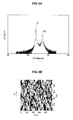
- FIG.4A is an XRD (X-ray diffraction) 2 ⁇ - ⁇ spectrum showing an X-ray diffraction measurement result of the crystal laminate structure 2 having the epitaxial crystal 20 which is manufactured by the method mentioned above so as to be constructed from one ⁇ -(AlGa) 2 O 3 layer with the Al content of 20%.
- a vertical axis of this graph shows X-ray scattering intensity expressed in logarithm.
- This graph shows a peak 1a due to the epitaxial growth substrate 1 and a sharp peak 20a due to the epitaxial crystal 20.
- a clear fringe is seen between the peak 1a and the peak 20a. Based on this clear fringe pattern, it is confirmed that a crystal laminate structure having a steep interface is formed.
- FIG.4B is an atomic force microscope image showing a surface state of the epitaxial crystal 20 which is manufactured by the method mentioned above so as to be constructed from one ⁇ -(AlGa) 2 O 3 layer with the Al content of 20%.
- An arrow-A in the drawing indicates a [100] direction of the epitaxial growth substrate 1. It is confirmed from this image that the epitaxial crystal 20 grows in a direction vertical or nearly vertical to the main surface 10 (the (010) plane) of the epitaxial growth substrate 1.
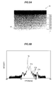
- FIG.5A is a Transmission Electron Microscope (TEM) observation image of a crystal laminate structure 2A in which plural (AlGa) 2 O 3 layers 21 and plural Ga 2 O 3 layers 22 are alternately formed by epitaxial growth on the main surface 10 of the epitaxial growth substrate 1.
- the shutters of the first cell 33 a and the second cell 33 b of the MBE system 3 are opened and closed to adjust the thicknesses of the (AlGa) 2 O 3 layers 21 and the Ga 2 O 3 layers 22 to predetermined thicknesses as well as to alternately laminate each layer, thereby forming the crystal laminate structure 2 A .
- the crystal laminate structure 2 A has six 6 nm-thick (AlGa) 2 O 3 layers 21 and five 4 nm-thick Ga 2 O 3 layers 22 which are alternately laminated on the epitaxial growth substrate 1.
- the (AlGa) 2 O 3 layers 21 and the Ga 2 O 3 layers 22 appeared in a stripe pattern can be clearly observed and it is thus understood that the layers having steep interface are formed with a highly accurate film thickness.
- FIG.5B is a graph of XRD 2 ⁇ - ⁇ spectrum showing the X-ray diffraction measurement result of the crystal laminate structure 2A shown in FIG.5A .
- This graph clearly shows the peak 1a due to the epitaxial growth substrate 1, plural satellite peaks 21a due to the plural (AlGa) 2 O 3 layers 21 and plural fringes 21 b therebetween and it is confirmed also from the X-ray diffraction measurement result that a crystal laminate structure having a steep interface is formed.
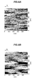
- FIGS.6 are atomic force microscope images each showing a surface state of an epitaxial crystal as Comparative Example in case that an epitaxial crystal formed of ⁇ -Ga 2 O 3 is grown by the same manufacturing method as mentioned above on the ( 100 ) plane or the (001) plane as the main surface of a ⁇ -Ga 2 O 3 -based single crystal substrate, wherein FIG.6A shows a surface state when the ( 100 ) plane is the main surface and FIG.6B shows a surface state when the ( 001 ) plane is the main surface.
- An arrow-B in FIG.6A and FIG.6B indicates a [ 010 ] direction of the substrate.
- needle-shaped crystals are grown in the [ 010 ] direction so as to be stacked in a direction vertical to the ( 100 ) plane or the ( 001 ) plane as the main surface in these Comparative Examples. This is considered a phenomenon caused because the growth rate in the [ 010 ] direction is faster than that in the [ 100 ] direction or the [ 001 ] direction.
- the present inventors have also confirmed that, when elements other than Ga and O (e.g., Al, In, Si, Sn, Mg, Zn, etc.) are added while using the ( 100 ) plane or the ( 001 ) plane as the main surface, such elements are unevenly distributed at a portion of the epitaxial crystal since a relation between the substrate plane orientation and the growth rate is different depending on elements and a homogeneous epitaxial crystal thus cannot be obtained.
- elements other than Ga and O e.g., Al, In, Si, Sn, Mg, Zn, etc.
- FIG.7B is a graph of XRD 2 ⁇ - ⁇ spectrum showing the X-ray diffraction measurement result of the crystal laminate structure shown in FIG.7A .
- the XRD 2 ⁇ - ⁇ spectrum in FIG.7B shows a peak 1 b due to diffraction from ⁇ -Ga 2 O 3 ( 400 ) plane of the epitaxial growth substrate and plural peaks 23a to 23c which are observed therearound and are considered to be derived from the crystal laminate structure composed of the (Al 1-x Ga x ) 2 O 3 layers and the Ga 2 O 3 layers.
- peaks 23a to 23c which are observed therearound and are considered to be derived from the crystal laminate structure composed of the (Al 1-x Ga x ) 2 O 3 layers and the Ga 2 O 3 layers.
- the main surface 10 is the ( 010 ) plane of the epitaxial growth substrate 1 formed of a ⁇ -Ga 2 O 3 -based single crystal, it is possible to provide a steep interface between the main surface 10 and the epitaxial crystal 20 formed thereon made of a Ga-containing oxide and it is also possible to form the epitaxial crystal 20 with a highly accurate thickness. In addition, it is possible to homogenize the epitaxial crystal 20 by suppressing unevenness in an amount of element incorporated thereinto.
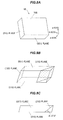
- FIG.8A is a perspective view showing an epitaxial growth substrate 1B in the modification of the first embodiment.
- the epitaxial growth substrate 1B is formed of a ⁇ -Ga 2 O 3 -based single crystal in the same manner as the above-mentioned epitaxial growth substrate 1 but is different from the above-mentioned epitaxial growth substrate 1 in that a ( 310 ) plane is a main surface 10B.
- FIG.8B is a sterical view showing the ( 310 ) plane of the ⁇ -Ga 2 O 3 -based single crystal.
- FIG.8C is a diagram illustrating an angle ⁇ formed between the ( 310 ) plane and the ( 010 ) plane of the ⁇ -Ga 2 O 3 -based single crystal.
- FIG.9 is an atomic force microscope image when observing a surface of the epitaxial crystal 20 which is formed on the main surface 10 B of the epitaxial growth substrate 1B using the method described above.
- An arrow-C in the drawing indicates a c-axis direction.
- the epitaxial crystal 20 does not grow in a needle shape but is formed to extend in a direction crossing the main surface 10 B .
- this epitaxial growth substrate 1B it is possible to obtain a crystal laminate structure which has a steep interface and allows the epitaxial crystal 20 to be formed with a highly accurate thickness.
- FIG.10 is a cross sectional view showing an example structure of a high-electron-mobility transistor (HEMT) which is an example of the semiconductor device in the present embodiment.
- HEMT high-electron-mobility transistor
- the epitaxial growth substrate 1 in the first embodiment is provided as an element substrate and an i-type ⁇ -(AlGa) 2 O 3 layer 41 as a first Ga-containing oxide layer and an n-type ⁇ -(AlGa) 2 O 3 layer 42 as a second Ga-containing oxide layer are laminated by epitaxial growth on the main surface 10 of the epitaxial growth substrate 1.
- a gate electrode 43 g, a source electrode 43 s and a drain electrode 43 d are provided on the n-type ⁇ -(AlGa) 2 O 3 layer 42.
- the gate electrode 43 g is in contact with a surface 42 a of the n-type ⁇ -(AlGa) 2 O 3 layer 42, thereby forming a Schottky junction. Meanwhile, the source electrode 43 s and the drain electrode 43 d are arranged with the gate electrode 43 g interposed therebetween and are in ohmic contact with the surface 42 a of the n-type ⁇ -(AlGa) 2 O 3 layer 42.
- the epitaxial growth substrate 1 in the second embodiment is doped with a predetermined amount of group II elements such as Mg and is thus formed to have high resistance.
- the i-type ⁇ -(AlGa) 2 O 3 layer 41 is an undoped electron transit layer and is formed by epitaxial growth on the main surface 10 of the epitaxial growth substrate 1. It is possible to form the i-type ⁇ -(AlGa) 2 O 3 layer 41 by mixing, e.g., not less than 5 percent by weight of ozone to the oxygen gas supplied from the gas supply pipe 35.
- the n-type ⁇ -(AlGa) 2 O 3 layer 42 is an electron supply layer doped with a donor such as Si or Sn and is formed by epitaxial growth on the i-type ⁇ -(AlGa) 2 O 3 layer 41.
- the i-type ⁇ -(AlGa) 2 O 3 layer 41 and the n-type ⁇ -(AlGa) 7 O 3 layer 42 have different band gaps, discontinuity of bands occurs at the interface therebetween, electrons generated from the donor in the n-type ⁇ -(AlGa) 2 O 3 layer 42 are concentrated on the i-type ⁇ -(AlGa) 2 O 3 layer 41 side and are distributed in a region in the vicinity of the interface, and an electron layer called two-dimensional electron gas is thereby formed.
- a first depletion layer due to the Schottky junction of the gate electrode 43g and a second depletion layer due to the formation of two-dimensional electron gas are produced in the n-type ⁇ -(AlGa) 2 O 3 layer 42.
- the n-type ⁇ -(AlGa) 2 O 3 layer 42 is formed in a thickness at which the first depletion layer is in contact with the second depletion layer.
- Voltage is applied to the gate electrode 43 g to change the thicknesses of the first and second depletion layers and to adjust the concentration of the two-dimensional electron gas, thereby allowing drain current to be controlled.
- the thickness of the i-type ⁇ -(AlGa) 2 O 3 layer 41 is not specifically limited but is desirably not less than 0.1 nm.
- the thickness of the n-type ⁇ -(AlGa) 2 O 3 layer 42 is set to 0.1 nm to 10 ⁇ m depending on a doping concentration.
- the i-type ⁇ -(AlGa) 2 O 3 layer 41 having a steep interface with a highly accurate thickness can be formed on the main surface 10 which is the ( 010 ) plane of the ⁇ -Ga 2 O 3 -based single crystal constituting the epitaxial growth substrate 1 and, as a result, it is possible to provide a steep interface between the i-type ⁇ -(AlGa) 2 O 3 layer 41 and the n-type ⁇ -(AlGa) 2 O 3 layer 42.
- FIG.11 is a cross sectional view showing an example structure of a MESFET (Metal-Semiconductor Field Effect Transistor) which is one type of field-effect transistors and is another example of the semiconductor device in the present embodiment.
- MESFET Metal-Semiconductor Field Effect Transistor
- the epitaxial growth substrate 1 in the first embodiment is provided as an element substrate and an n-type ⁇ -Ga 2 O 3 layer 51 formed by epitaxial growth is provided on the main surface 10 (the ( 010 ) plane) of the epitaxial growth substrate 1.
- a gate electrode 52 g , a source electrode 52s and a drain electrode 52d are provided on the n-type ⁇ -Ga 2 O 3 layer 51.
- the gate electrode 52 g is in contact with a surface 51 a of the n-type ⁇ -Ga 2 O 3 layer 51 , thereby forming a Schottky junction. Meanwhile, the source electrode 52 s and the drain electrode 52 d are arranged with the gate electrode 52 g interposed therebetween and are in ohmic contact with the surface 51 a of the n-type ⁇ -Ga 2 O 3 layer 51 .
- the donor concentration is high in the vicinity of contact areas with the source electrode 52 s and with the drain electrode 52 d because of addition of Si or Sn, etc. Meanwhile, the donor concentration in the other region including a contact area with the gate electrode 52g is lower than in the vicinity of the contact areas with the source electrode 52 s and with the drain electrode 52 d.
- the epitaxial growth substrate 1 in the third embodiment is doped with a predetermined amount of group II elements such as Mg and is thus formed to have high resistance.
- the thickness of the depletion layer in the n-type ⁇ -Ga 2 O 3 layer 51 is changed by adjusting bias voltage applied to the gate electrode 52 g , thereby allowing drain current to be controlled.
- the n-type ⁇ -Ga 2 O 3 layer 51 having a steep interface a highly accurate thickness can be formed on the main surface 10 which is the ( 010 ) plane of the ⁇ -Ga 2 O 3 -based single crystal constituting the epitaxial growth substrate 1 . Therefore, it is possible to produce the MESFET 5 with high performance and stable quality.
- FIG.12 is a cross sectional view showing an example structure of a Schottky-barrier diode which is another example of the semiconductor device in the present embodiment.
- the epitaxial growth substrate 1 in the first embodiment is provided as an element substrate and an n-type ⁇ -Ga 2 O 3 layer 61 formed by epitaxial growth is provided on the main surface 10 (the ( 010 ) plane) of the epitaxial growth substrate 1.
- a Schottky electrode 62 is provided on the n-type ⁇ -Ga 2 O 3 layer 61 and is in Schottky-contact with a surface 61 a of the n-type ⁇ -Ga 2 O 3 layer 61. Meanwhile, an ohmic electrode 63 is provided on a surface of the epitaxial growth substrate 1 opposite to the n-type ⁇ -Ga 2 O 3 layer 61 and is ohmic contact with the epitaxial growth substrate 1.
- the epitaxial growth substrate 1 in the fourth embodiment is formed to have an n-type conductivity by oxygen loss or impurity doping.
- the n-type ⁇ -Ga 2 O 3 layer 61 is formed to have a lower donor concentration than the epitaxial growth substrate 1.
- the n-type ⁇ -Ga 2 O 3 layer 61 having a steep interface with a highly accurate thickness can be formed on the main surface 10 which is the ( 010 ) plane of the ⁇ -Ga 2 O 3 -based single crystal constituting the epitaxial growth substrate 1. Therefore, it is possible to produce the Schottky diode 6 with high performance and stable quality.
- the main surface is the ( 010 ) plane or the ( 310 ) plane of the ⁇ -Ga 2 O 3 -based single crystal in the above-mentioned first embodiment and the modification thereof
- the main surface may be a plane between the ( 010 ) plane and the ( 310 ) plane.
- the main surface may be a plane inclined at an angle equal to or smaller than 37.5° in a direction other than the direction between the ( 010 ) plane and the ( 310 ) plane.
- the high-electron-mobility transistor may be formed by providing the i-type ⁇ -(AlGa) 2 O 3 layer 41 on the epitaxial growth substrate 1B having the ( 310 ) plane as the main surface 10B.
- the main surface may be a plane inclined at an angle equal to or smaller than 37.5° from the ( 010 ) plane and the i-type ⁇ -(AlGa) 2 O 3 layer 41 may be formed on such a main surface.
- the main surface may be a plane inclined at an angle equal to or smaller than 37.5° from the (010) plane and the n-type ⁇ -Ga 2 O 3 layer 51 /the n-type ⁇ -Ga 2 O 3 layer 61 may be formed on such a main surface.
- An epitaxial growth substrate which allows an improvement in the crystalline quality of a Ga-containing oxide layer formed on the ⁇ -Ga 2 O 3 single crystal substrate, and a crystal laminate structure are provided.
Landscapes
- Chemical & Material Sciences (AREA)
- Crystallography & Structural Chemistry (AREA)
- Engineering & Computer Science (AREA)
- Materials Engineering (AREA)
- Metallurgy (AREA)
- Organic Chemistry (AREA)
- Inorganic Chemistry (AREA)
- Crystals, And After-Treatments Of Crystals (AREA)
- Physical Vapour Deposition (AREA)
- Junction Field-Effect Transistors (AREA)
- Physical Deposition Of Substances That Are Components Of Semiconductor Devices (AREA)
- Electrodes Of Semiconductors (AREA)
Abstract
Description
- The invention relates to an epitaxial growth substrate (or substrate for epitaxial growth) and, in particular, to an epitaxial growth substrate that includes a β-Ga2O3-based single crystal and a crystal laminate structure (or laminated crystal structure).
- A semiconductor element is known in which a Ga-containing oxide is deposited on an element substrate formed of a β-Ga2O3-based single crystal (see, e.g., PTL 1).
- This type of semiconductor element is formed by laminating a layer of n-type or p-type conductivity on a main surface of a β-Ga2O3 single crystal substrate using a physical vapor-phase growth method such as MBE (Molecular Beam Epitaxy) or a chemical vapor-phase growth method such as CVD (Chemical Vapor Deposition).
- In addition, a (100) plane having high cleavability and thus providing a flat surface easily is used as the main surface of the β-Ga2O3 single crystal substrate (see, e.g., PTL 2).
-
- [PTL 1]
JP-A-2005-235961 - [PTL 2]
JP-A-2008-156141 - Recently, for further improvement in performance of semiconductor elements, the challenge is how to form a steep interface between the element substrate and an epitaxial layer formed thereon and between laminated epitaxial layers and how to form an epitaxial layer with a highly accurate thickness.
- It is an object of the invention to provide an epitaxial growth substrate that allows an improvement in the crystalline quality of a Ga-containing oxide layer formed on the β-Ga2O3 single crystal substrate, as well as a crystal laminate structure.
- The present inventors have conducted researches for achieving the above object and found that the crystalline quality of the Ga-containing oxide layer formed on the β-Ga2O3 single crystal substrate depends on which crystal surface of the β-Ga2O3 single crystal substrate is used as the main surface. Then, the present invention has been completed by repeating further experiments.
- The present invention is based on findings obtained by the experiments and offers the epitaxial growth substrate and the crystal laminate structure below.
- [1] An epitaxial growth substrate, comprising:
- a β-Ga2O3-based single crystal; and
- a (010) plane or a plane inclined at an angle not more than 37.5° with respect to the (010) plane as a main surface thereof.
- [2] The epitaxial growth substrate according to [1], wherein the main surface comprises a (010) plane or a plane between the (010) plane and a (310) plane of the β-Ga2O3-based single crystal.
- [3] The epitaxial growth substrate according to [2], wherein the main surface comprises the (010) plane or the (310) plane of the β-Ga2O3-based single crystal.
- [4] A crystal laminate structure, comprising:
- an epitaxial growth substrate comprising a β-Ga2O3-based single crystal and a (010) plane or a plane inclined at an angle not more than 37.5° with respect to the (010) plane as a main surface thereof; and
- an epitaxial crystal formed on the main surface of the epitaxial growth substrate and comprising a Ga-containing oxide.
- [5] The crystal laminate structure according to [4], wherein the main surface comprises a (010) plane or a plane between the (010) plane and a (310) plane of the β-Ga2O3-based single crystal.
- [6] The crystal laminate structure according to [5], wherein the main surface comprises the (010) plane or the (310) plane of the β-Ga2O3-based single crystal.
- According to an embodiment of the invention, the crystalline quality of the Ga-containing oxide layer formed on the β-Ga2O3 single crystal substrate can be improved.
-
- [
FIG.1A ]
FIG.1A is a perspective view showing an epitaxial growth substrate in a first embodiment. - [
FIG.1B ]
FIG.1B is a sterical view showing a crystal structure by which the plane orientation of the epitaxial growth substrate ofFIG.1A is defined. - [
FIG.2 ]
FIG.2 is a cross sectional view showing an example structure of a crystal laminate structure. - [
FIG.3 ]
FIG.3 is a cross sectional view showing an MBE system used for forming the crystal laminate structure. - [
FIG.4A ]
FIG.4A is an XRD 2θ-θ spectrum showing an X-ray diffraction measurement result of the crystal laminate structure when only one (AlGa)2O3 layer with an Al content of 20% is epitaxially grown on the epitaxial growth substrate. - [
FIG.4B ]
FIG.4B is an atomic force microscope image showing a surface state of an epitaxial crystal. - [
FIG.5A ]
FIG.5A is a TEM observation image of a crystal laminate structure in which plural (AlGa)2O3 layers and Ga2O3 layers are alternately formed. - [
FIG.5B ]
FIG.5B is an XRD 2θ-θ spectrum of the crystal laminate structure. - [
FIG.6A ]
FIG.6A is an atomic force microscope image showing a surface state of an epitaxial crystal which is shown as a Comparative Example and is grown so as to have a (100) plane as a main surface. - [
FIG.6B ]
FIG.6B is an atomic force microscope image showing a surface state of an epitaxial crystal which is shown as a Comparative Example and is grown so as to have a (001) plane as a main surface. - [
FIG.7A ]
FIG.7A is a TEM observation image of a crystal laminate structure in which plural (AlGa)2O3 layers and Ga2O3 layers are alternately formed on an epitaxial growth substrate formed of a β-Ga2O3-based single crystal having a (100) plane as a main surface. - [
FIG.7B ]
FIG.7B is an XRD 2θ-θ spectrum of the crystal laminate structure ofFIG.7A . - [
FIG.8A ]
FIG.8A is a perspective view showing an epitaxial growth substrate in a modification of the first embodiment. - [
FIG.8B ]
FIG.8B is a sterical view showing a (310) plane of the β-Ga2O3-based single crystal. - [
FIG.8C ]
FIG.8C is a diagram illustrating an angle δ defined between the (310) plane and the (010) plane of the β-Ga2O3-based single crystal. - [
FIG.9 ]
FIG.9 is an atomic force microscope image obtained when observing a surface of an epitaxial crystal formed on the (310) plane of the epitaxial growth substrate. - [
FIG.10 ]
FIG.10 is a cross sectional view showing an example structure of a high-electron-mobility transistor in a second embodiment of the present invention. - [
FIG.11 ]
FIG.11 is a cross sectional view showing an example structure of a MESFET in a third embodiment of the invention. - [
FIG.12 ]
FIG.12 is a cross sectional view showing an example structure of a Schottky-barrier diode in a fourth embodiment of the invention. -
FIG.1A is a perspective view showing an epitaxial growth substrate in the first embodiment of the invention. Thisepitaxial growth substrate 1 is formed of a β-Ga2O3 (gallium oxide)-based single crystal and has a (010) plane as amain surface 10. - The
epitaxial growth substrate 1 is formed in a plate shape having predetermined plane orientations. Orientation axes of the β-Ga2O3 crystal structure includes an a-axis <100>, a b-axis <010> and a c-axis <001>, and theepitaxial growth substrate 1 is formed in a plate shape having the predetermined plane orientations defined by these three axes, i.e., a (010) plane, a (100) plane and a (001) plane. Of those, the (010) plane is themain surface 10 used for epitaxially growing a crystal of Ga-containing oxide when manufacturing a semiconductor element and is formed so as to have a larger area than other planes. -
FIG.1B is a sterical view showing a crystal structure in which plane orientations of the epitaxial growth substrate ofFIG.1A are defined. β-Ga2O3 is a monoclinic crystal and is formed so that α=γ=90°, β=103.8°, α-axis lattice constant (a0)=12.23Å, b-axis lattice constant (b0)=3.04Å and c-axis lattice constant (c0)=5.8Å. - It should be noted that, the
epitaxial growth substrate 1 is basically formed of a β-Ga2O3 single crystal as described above but may be formed of an oxide including mainly Ga doped with one or more elements selected from the three consisting of Cu, Ag, Zn, Cd, Al, In, Si, Ge and Sn. It is possible to control a lattice constant, bandgap energy or electrical conduction properties by adding such elements. When adding, e.g., elements of Al and In, it is possible to obtain theepitaxial growth substrate 1 represented by (GaxAlyIn(1-x-y)2O3 (where 0<x≤1, 0≤y≤1, 0<x+y≤1). The band gap is widened by adding Al and is narrowed by adding In. - For manufacturing the
epitaxial growth substrate 1, a bulk crystal is firstly made by the FZ (Floating Zone) method or the EFG (Edge Defined Film Fed Growth) method, etc., and is then cut out and formed into a plate shape by cutting or cleaving. - In case of using the FZ method, a bulk crystal is formed using, e.g., an infrared-heating single crystal manufacturing system. In detail, firstly, an end of a seed crystal is held on a seed chuck and an upper end portion of a rod-like polycrystalline raw material is held on a raw-material chuck. After adjusting a vertical position of an upper rotating shaft, the top edge of the seed crystal is brought into contact with the lower edge of the polycrystalline raw material. The vertical position of the upper rotating shaft and that of a lower rotating shaft are adjusted so that light of halogen lamp is focused on the upper edge of the seed crystal and the lower edge of the polycrystalline raw material. After the adjustment, the upper edge of the seed crystal and the lower edge of the polycrystalline raw material are heated the heated portion is melted, thereby forming melt droplets. At this time, only the seed crystal is being rotated. The aforementioned portion is melted while rotating the polycrystalline raw material and the seed crystal in opposite directions so as to be mixed sufficiently and the polycrystalline raw material and the seed crystal are then pulled in directions opposite to each other to form a single crystal having appropriate length and thickness, thereby making a bulk crystal.
- In case of using the EFG method, a predetermined amount of β-Ga2O3 to be a raw material is put in a crucible and is melted by heating, thereby forming β-Ga2O3 melt. Through a slit formed on a slit die which is placed in the crucible, the β-Ga2O3 melt is drawn up to an upper surface of the slit die by capillary action, the β-Ga2O3 melt is cooled by contact with the seed crystal and a bulk crystal having an arbitrary cross sectional shape is thereby formed.
- It should be noted that, the β-Ga2O3 bulk crystals made by these methods may be doped with impurities for the purpose of obtaining a desired conductivity type.
- The β-Ga2O3 bulk crystal formed as described above is shaped by, e.g., a wire saw so that the (010) plane is exposed as a main surface, thereby obtaining thin sheet-like β-Ga2O3 having a desired shape with a thickness of, e.g., 1 mm. After grinding and polishing until the thickness becomes about 600 µm, the
epitaxial growth substrate 1 is obtained. - Subsequently, the
epitaxial growth substrate 1 is subjected to organic cleaning in order of methanol, acetone and methanol for three minutes each and is further subjected to running water cleaning using ultrapure water, hydrofluoric acid immersion cleaning for fifteen minutes, sulfuric acid/hydrogen peroxide mixture immersion cleaning for five minutes and then running water cleaning using ultrapure water. After the subsequent thermal cleaning at 800°C for ten minutes, the main surface of theepitaxial growth substrate 1 is ready for epitaxial growth of a Ga-containing oxide. - Next, a crystal laminate structure and a forming method thereof in the present embodiment will be described in reference to
FIGS.2 and3 . -
FIG.2 is a cross sectional view showing an example structure of a crystal laminate structure in the present embodiment. Acrystal laminate structure 2 is formed by laminating anepitaxial crystal 20 made of a Ga-containing oxide on themain surface 10 of theepitaxial growth substrate 1 described above. - The
epitaxial crystal 20 is a crystalline body having, e.g., a β-Gallia structure containing Ga, and in more detail, is a crystalline body including mainly Ga2O3 or a mixed crystalline body containing Ga2O3 and more than 0 wt% and not more than 60 wt% of Al2O3 in the form of a crystal layer mainly having a β-Gallia structure. In addition, an impurity determining a conductivity type may be added to theepitaxial crystal 20. - The method of forming the
epitaxial crystal 20 on themain surface 10 of theepitaxial growth substrate 1 is, e.g., PLD (Pulsed Laser Deposition), CVD (Chemical Vapor Deposition), sputtering and MBE (Molecular Beam Epitaxy) etc. In the present embodiment, a thin film growth method using the MBE is employed. The MBE is a crystal growth method in which a single or compound solid is heated in an evaporation source called cell and vapor generated by heat is supplied as a molecular beam onto the surface of the substrate. -
FIG.3 is a cross sectional view showing an MBE system used for forming thecrystal laminate structure 2. AnMBE system 3 is provided with avacuum chamber 30, asubstrate holder 31 supported in thevacuum chamber 30 to hold theepitaxial growth substrate 1,heating devices 32 held on thesubstrate holder 31, plural cells 33 (33a, 33b, 33c, 33d) each provided for each atom or molecule constituting theepitaxial crystal 20, heaters 34 (34a, 34b, 34c, 34d) for hearing the plural cells 33, agas supply pipe 35 for supplying oxygen gas into thevacuum chamber 30, and avacuum pump 36 for exhausting the air in thevacuum chamber 30. It is configured that thesubstrate holder 31 can be rotated by a non-illustrated motor via ashaft 310. - Ga to be a material of the
epitaxial crystal 20 is loaded in thefirst cell 33a. Al also to be a material of theepitaxial crystal 20 is loaded in thesecond cell 33b. Meanwhile, a material to be doped as a donor, such as Si or Sn, is loaded in thethird cell 33c. A material to be doped as an acceptor, such as Mg or Zn, is loaded in thefourth cell 33d. Each of the first tofourth cells 33a to 33d is provided with a non-illustrated shutter and is configured to be closed by the shutter when not necessary. - Next, a manufacturing procedure of the
crystal laminate structure 2 will be described. Firstly, theepitaxial growth substrate 1 is attached to thesubstrate holder 31 of theMBE system 3. Next, thevacuum pump 36 is activated to reduce atmospheric pressure in thevacuum chamber 30 to about 10-10 Torr. Then, theepitaxial growth substrate 1 is heated by theheating devices 32. - After the
epitaxial growth substrate 1 is heated to a predetermined temperature, oxygen gas produced by a non-illustrated oxygen generator is supplied into thevacuum chamber 30 through thegas supply pipe 35. - In case of making a crystal formed of Ga2O3 as the
epitaxial crystal 20, thefirst heater 34a of thefirst cell 33a is heated while rotating thesubstrate holder 31 after supplying the oxygen gas into thevacuum chamber 30 so that Ga vapor is started to be supplied. Meanwhile, in case of making a mixed crystal of Ga2O3 and Al2O3 as theepitaxial crystal 20, thefirst heater 34a of thefirst cell 33a and thesecond heater 34b of thesecond cell 33b are heated while rotating thesubstrate holder 31 so that Ga vapor and Al vapor are started to be supplied. - Growth conditions of the
epitaxial crystal 20 in case of making a crystal formed of Ga2O3 as theepitaxial crystal 20 are, e.g., a growth temperature of 700°C, Ga beam-equivalent pressure (BEP) of 3x10⁻⁵ Pa and growth time of 1 hour. Meanwhile, in case of making a mixed crystal of Ga2O3 and Al2O3 as theepitaxial crystal 20, some of the above-mentioned growth conditions can be such that the Ga beam-equivalent pressure is 1.5x10⁻⁵ Pa and Al beam-equivalent pressure is, e.g., 5x10⁻⁷ Pa. - Accordingly, the
epitaxial crystal 20 formed of a Ga-containing oxide is grown on themain surface 10 of theepitaxial growth substrate 1 and thecrystal laminate structure 2 is thereby obtained. - Meanwhile, when imparting an n-type conductivity to the
epitaxial crystal 20, the material to be a donor such as Si or Sn is supplied from thethird cell 33c by heating thethird heater 34c. On the other hand, when imparting a p-type conductivity, the material to be an acceptor such as Mg or Zn is supplied from thefourth cell 33d by heating thefourth heater 34d. -
FIG.4A is an XRD (X-ray diffraction) 2θ-θ spectrum showing an X-ray diffraction measurement result of thecrystal laminate structure 2 having theepitaxial crystal 20 which is manufactured by the method mentioned above so as to be constructed from one β-(AlGa)2O3 layer with the Al content of 20%. A vertical axis of this graph shows X-ray scattering intensity expressed in logarithm. This graph shows apeak 1a due to theepitaxial growth substrate 1 and asharp peak 20a due to theepitaxial crystal 20. In addition, a clear fringe is seen between thepeak 1a and thepeak 20a. Based on this clear fringe pattern, it is confirmed that a crystal laminate structure having a steep interface is formed. -
FIG.4B is an atomic force microscope image showing a surface state of theepitaxial crystal 20 which is manufactured by the method mentioned above so as to be constructed from one β-(AlGa)2O3 layer with the Al content of 20%. An arrow-A in the drawing indicates a [100] direction of theepitaxial growth substrate 1. It is confirmed from this image that theepitaxial crystal 20 grows in a direction vertical or nearly vertical to the main surface 10 (the (010) plane) of theepitaxial growth substrate 1. -
FIG.5A is a Transmission Electron Microscope (TEM) observation image of acrystal laminate structure 2A in which plural (AlGa)2O3 layers 21 and plural Ga2O3 layers 22 are alternately formed by epitaxial growth on themain surface 10 of theepitaxial growth substrate 1. The shutters of thefirst cell 33a and thesecond cell 33b of theMBE system 3 are opened and closed to adjust the thicknesses of the (AlGa)2O3 layers 21 and the Ga2O3 layers 22 to predetermined thicknesses as well as to alternately laminate each layer, thereby forming thecrystal laminate structure 2A. - As shown in the TEM observation image, the
crystal laminate structure 2A has six 6 nm-thick (AlGa)2O3 layers 21 and five 4 nm-thick Ga2O3 layers 22 which are alternately laminated on theepitaxial growth substrate 1. The (AlGa)2O3 layers 21 and the Ga2O3 layers 22 appeared in a stripe pattern can be clearly observed and it is thus understood that the layers having steep interface are formed with a highly accurate film thickness. -
FIG.5B is a graph of XRD 2θ-θ spectrum showing the X-ray diffraction measurement result of thecrystal laminate structure 2A shown inFIG.5A . This graph clearly shows thepeak 1a due to theepitaxial growth substrate 1,plural satellite peaks 21a due to the plural (AlGa)2O3 layers 21 andplural fringes 21b therebetween and it is confirmed also from the X-ray diffraction measurement result that a crystal laminate structure having a steep interface is formed. -
FIGS.6 are atomic force microscope images each showing a surface state of an epitaxial crystal as Comparative Example in case that an epitaxial crystal formed of β-Ga2O3 is grown by the same manufacturing method as mentioned above on the (100) plane or the (001) plane as the main surface of a β-Ga2O3-based single crystal substrate, whereinFIG.6A shows a surface state when the (100) plane is the main surface andFIG.6B shows a surface state when the (001) plane is the main surface. An arrow-B inFIG.6A and FIG.6B indicates a [010] direction of the substrate. - As shown in
FIG.6A and FIG.6B , it is understood that needle-shaped crystals are grown in the [010] direction so as to be stacked in a direction vertical to the (100) plane or the (001) plane as the main surface in these Comparative Examples. This is considered a phenomenon caused because the growth rate in the [010] direction is faster than that in the [100] direction or the [001] direction. - The present inventors have also confirmed that, when elements other than Ga and O (e.g., Al, In, Si, Sn, Mg, Zn, etc.) are added while using the (100) plane or the (001) plane as the main surface, such elements are unevenly distributed at a portion of the epitaxial crystal since a relation between the substrate plane orientation and the growth rate is different depending on elements and a homogeneous epitaxial crystal thus cannot be obtained.
-
FIG.7A is a transmission electron microscope observation image of a crystal laminate structure when plural (Al1-xGax)2O3 layers (x=0.6) and plural Ga2O3 layers are alternately formed by epitaxial growth using theMBE system 3 on an epitaxial growth substrate formed of a β-Ga2O3-based single crystal having a (100) plane as a main surface. Meanwhile,FIG.7B is a graph of XRD 2θ-θ spectrum showing the X-ray diffraction measurement result of the crystal laminate structure shown inFIG.7A . - As shown in
FIG.7A , in this crystal laminate structure, an interface between the (Al1-xGax)2O3 layer and the Ga2O3 layer is unclear and a stripe pattern such as shown inFIG.5A is not observed. Meanwhile, the XRD 2θ-θ spectrum inFIG.7B shows apeak 1b due to diffraction from β-Ga2O3 (400) plane of the epitaxial growth substrate andplural peaks 23a to 23c which are observed therearound and are considered to be derived from the crystal laminate structure composed of the (Al1-xGax)2O3 layers and the Ga2O3 layers. However, there is no periodicity in the intervals of these peaks and it is thus considered that a good laminate structure cannot be formed. - In the first embodiment, since the
main surface 10 is the (010) plane of theepitaxial growth substrate 1 formed of a β-Ga2O3-based single crystal, it is possible to provide a steep interface between themain surface 10 and theepitaxial crystal 20 formed thereon made of a Ga-containing oxide and it is also possible to form theepitaxial crystal 20 with a highly accurate thickness. In addition, it is possible to homogenize theepitaxial crystal 20 by suppressing unevenness in an amount of element incorporated thereinto. - Next, a modification of the first embodiment of the invention will be described in reference to
FIGS.8 . -
FIG.8A is a perspective view showing anepitaxial growth substrate 1B in the modification of the first embodiment. Theepitaxial growth substrate 1B is formed of a β-Ga2O3-based single crystal in the same manner as the above-mentionedepitaxial growth substrate 1 but is different from the above-mentionedepitaxial growth substrate 1 in that a (310) plane is amain surface 10B. -
FIG.8B is a sterical view showing the (310) plane of the β-Ga2O3-based single crystal. Meanwhile,FIG.8C is a diagram illustrating an angle δ formed between the (310) plane and the (010) plane of the β-Ga2O3-based single crystal. As shown in these drawings, the (310) plane of the β-Ga2O3-based single crystal is a plane which is inclined at an angle δ=37.5° with respect to the (010) plane. - It is possible to obtain a crystal laminate structure by forming the
epitaxial crystal 20 on themain surface 10B (the (310) plane) of thisepitaxial growth substrate 1B using the same method as described above. -
FIG.9 is an atomic force microscope image when observing a surface of theepitaxial crystal 20 which is formed on themain surface 10B of theepitaxial growth substrate 1B using the method described above. An arrow-C in the drawing indicates a c-axis direction. - As shown in this drawing, the
epitaxial crystal 20 does not grow in a needle shape but is formed to extend in a direction crossing themain surface 10B. - Also in case of using this
epitaxial growth substrate 1B, it is possible to obtain a crystal laminate structure which has a steep interface and allows theepitaxial crystal 20 to be formed with a highly accurate thickness. In addition, it is possible to homogenize theepitaxial crystal 20 by suppressing unevenness in an amount of element incorporated thereinto. In other words, it is possible to achieve the same effects as those described in the first embodiment even by the epitaxial growth substrate of which main surface is a plane inclined at an angle equal to or smaller than 37.5° with respect to the (010) plane. - Next, the second embodiment of the invention will be described in reference to
FIG.10. FIG.10 is a cross sectional view showing an example structure of a high-electron-mobility transistor (HEMT) which is an example of the semiconductor device in the present embodiment. - In this high-electron-
mobility transistor 4, theepitaxial growth substrate 1 in the first embodiment is provided as an element substrate and an i-type β-(AlGa)2O3 layer 41 as a first Ga-containing oxide layer and an n-type β-(AlGa)2O3 layer 42 as a second Ga-containing oxide layer are laminated by epitaxial growth on themain surface 10 of theepitaxial growth substrate 1. In addition, agate electrode 43g, asource electrode 43s and adrain electrode 43d are provided on the n-type β-(AlGa)2O3 layer 42. - The
gate electrode 43g is in contact with asurface 42a of the n-type β-(AlGa)2O3 layer 42, thereby forming a Schottky junction. Meanwhile, thesource electrode 43s and thedrain electrode 43d are arranged with thegate electrode 43g interposed therebetween and are in ohmic contact with thesurface 42a of the n-type β-(AlGa)2O3 layer 42. - While the β-(AlGa)2O3 single crystal generally has an n-type conductivity due to oxygen defects, the
epitaxial growth substrate 1 in the second embodiment is doped with a predetermined amount of group II elements such as Mg and is thus formed to have high resistance. - The i-type β-(AlGa)2O3 layer 41 is an undoped electron transit layer and is formed by epitaxial growth on the
main surface 10 of theepitaxial growth substrate 1. It is possible to form the i-type β-(AlGa)2O3 layer 41 by mixing, e.g., not less than 5 percent by weight of ozone to the oxygen gas supplied from thegas supply pipe 35. - The n-type β-(AlGa)2O3 layer 42 is an electron supply layer doped with a donor such as Si or Sn and is formed by epitaxial growth on the i-type β-(AlGa)2O3 layer 41.
- Since the i-type β-(AlGa)2O3 layer 41 and the n-type β-(AlGa)7O3 layer 42 have different band gaps, discontinuity of bands occurs at the interface therebetween, electrons generated from the donor in the n-type β-(AlGa)2O3 layer 42 are concentrated on the i-type β-(AlGa)2O3 layer 41 side and are distributed in a region in the vicinity of the interface, and an electron layer called two-dimensional electron gas is thereby formed.
- As such, a first depletion layer due to the Schottky junction of the
gate electrode 43g and a second depletion layer due to the formation of two-dimensional electron gas are produced in the n-type β-(AlGa)2O3 layer 42. The n-type β-(AlGa)2O3 layer 42 is formed in a thickness at which the first depletion layer is in contact with the second depletion layer. - Voltage is applied to the
gate electrode 43g to change the thicknesses of the first and second depletion layers and to adjust the concentration of the two-dimensional electron gas, thereby allowing drain current to be controlled. - The thickness of the i-type β-(AlGa)2O3 layer 41 is not specifically limited but is desirably not less than 0.1 nm. In addition, the thickness of the n-type β-(AlGa)2O3 layer 42 is set to 0.1 nm to 10 µm depending on a doping concentration.
- In the second embodiment, the i-type β-(AlGa)2O3 layer 41 having a steep interface with a highly accurate thickness can be formed on the
main surface 10 which is the (010) plane of the β-Ga2O3-based single crystal constituting theepitaxial growth substrate 1 and, as a result, it is possible to provide a steep interface between the i-type β-(AlGa)2O3 layer 41 and the n-type β-(AlGa)2O3 layer 42. In addition, it is possible to form the n-type β-(AlGa)2O3 layer 42 with a highly accurate thickness. It is therefore possible to produce the high-electron-mobility transistor 4 with high performance and stable quality. - Next, the third embodiment of the invention will be described in reference to
FIG.11. FIG.11 is a cross sectional view showing an example structure of a MESFET (Metal-Semiconductor Field Effect Transistor) which is one type of field-effect transistors and is another example of the semiconductor device in the present embodiment. - In this
MESFET 5, theepitaxial growth substrate 1 in the first embodiment is provided as an element substrate and an n-type β-Ga2O3 layer 51 formed by epitaxial growth is provided on the main surface 10 (the (010) plane) of theepitaxial growth substrate 1. In addition, agate electrode 52g, asource electrode 52s and adrain electrode 52d are provided on the n-type β-Ga2O3 layer 51. - The
gate electrode 52g is in contact with asurface 51a of the n-type β-Ga2O3 layer 51, thereby forming a Schottky junction. Meanwhile, thesource electrode 52s and thedrain electrode 52d are arranged with thegate electrode 52g interposed therebetween and are in ohmic contact with thesurface 51a of the n-type β-Ga2O3 layer 51. - In the n-type β-Ga2O3 layer 51, the donor concentration is high in the vicinity of contact areas with the
source electrode 52s and with thedrain electrode 52d because of addition of Si or Sn, etc. Meanwhile, the donor concentration in the other region including a contact area with thegate electrode 52g is lower than in the vicinity of the contact areas with thesource electrode 52s and with thedrain electrode 52d. - The
epitaxial growth substrate 1 in the third embodiment is doped with a predetermined amount of group II elements such as Mg and is thus formed to have high resistance. - In the
MESFET 5 configured as described above, the thickness of the depletion layer in the n-type β-Ga2O3 layer 51 is changed by adjusting bias voltage applied to thegate electrode 52g, thereby allowing drain current to be controlled. - In the third embodiment, the n-type β-Ga2O3 layer 51 having a steep interface a highly accurate thickness can be formed on the
main surface 10 which is the (010) plane of the β-Ga2O3-based single crystal constituting theepitaxial growth substrate 1. Therefore, it is possible to produce theMESFET 5 with high performance and stable quality. - Next, the fourth embodiment of the invention will be described in reference to
FIG.12 FIG.12 is a cross sectional view showing an example structure of a Schottky-barrier diode which is another example of the semiconductor device in the present embodiment. - In this Schottky-
barrier diode 6, theepitaxial growth substrate 1 in the first embodiment is provided as an element substrate and an n-type β-Ga2O3 layer 61 formed by epitaxial growth is provided on the main surface 10 (the (010) plane) of theepitaxial growth substrate 1. - A
Schottky electrode 62 is provided on the n-type β-Ga2O3 layer 61 and is in Schottky-contact with asurface 61a of the n-type β-Ga2O3 layer 61. Meanwhile, anohmic electrode 63 is provided on a surface of theepitaxial growth substrate 1 opposite to the n-type β-Ga2O3 layer 61 and is ohmic contact with theepitaxial growth substrate 1. - In addition, the
epitaxial growth substrate 1 in the fourth embodiment is formed to have an n-type conductivity by oxygen loss or impurity doping. The n-type β-Ga2O3 layer 61 is formed to have a lower donor concentration than theepitaxial growth substrate 1. - When forward voltage (electric potential is positive on the
Schottky electrode 62 side) is applied to theSchottky diode 6, electric current is increased due to electron transfer from theepitaxial growth substrate 1 to the n-type β-Ga2O3 layer 61. As a result, a forward current flows from theSchottky electrode 62 to theohmic electrode 63. - On the other hand, when reverse voltage (electric potential is negative on the
Schottky electrode layer 2 side) is applied to theSchottky diode 6, substantially no electric current flows through theSchottky diode 6. - In the fourth embodiment, the n-type β-Ga2O3 layer 61 having a steep interface with a highly accurate thickness can be formed on the
main surface 10 which is the (010) plane of the β-Ga2O3-based single crystal constituting theepitaxial growth substrate 1. Therefore, it is possible to produce theSchottky diode 6 with high performance and stable quality. - Although the preferred embodiments of the invention have been described above, the present invention is not intended to be limited to these embodiments, and the various kinds of modifications and applications can be implemented without departing from the gist thereof.
- Although, for example, the main surface is the (010) plane or the (310) plane of the β-Ga2O3-based single crystal in the above-mentioned first embodiment and the modification thereof, the main surface may be a plane between the (010) plane and the (310) plane. Alternatively, the main surface may be a plane inclined at an angle equal to or smaller than 37.5° in a direction other than the direction between the (010) plane and the (310) plane.
- In addition, although the i-type β-(AlGa)2O3 layer 41 is formed on the
epitaxial growth substrate 1 having the (010) plane as themain surface 10 in the second embodiment, the high-electron-mobility transistor may be formed by providing the i-type β-(AlGa)2O3 layer 41 on theepitaxial growth substrate 1B having the (310) plane as themain surface 10B. Furthermore, the main surface may be a plane inclined at an angle equal to or smaller than 37.5° from the (010) plane and the i-type β-(AlGa)2O3 layer 41 may be formed on such a main surface. - In addition, although the n-type β-Ga2O3 layer 51/the n-type β-Ga2O3 layer 61 is formed on the
epitaxial growth substrate 1 having the (010) plane as themain surface 10 in the third/fourth embodiment, the main surface may be a plane inclined at an angle equal to or smaller than 37.5° from the (010) plane and the n-type β-Ga2O3 layer 51/the n-type β-Ga2O3 layer 61 may be formed on such a main surface. - In addition, although the case where the invention is applied to the epitaxial growth substrate of the high-electron-mobility transistor, the MESFET and the Schottky-barrier diode has been described in the second to fourth embodiments, semiconductor devices to which the invention is applied are not limited thereto.
- An epitaxial growth substrate, which allows an improvement in the crystalline quality of a Ga-containing oxide layer formed on the β-Ga2O3 single crystal substrate, and a crystal laminate structure are provided.
-
- 1, 1B: epitaxial growth substrate
- 2, 2A: crystal laminate structure
- 3: MBE system
- 4: high-electron-mobility transistor
- 5: MESFET
- 6: Schottky-barrier diode
- 10, 10B: main surface
- 20: epitaxial crystal
- 20a: satellite peak
- 21: ((AlGa)2O3 layer
- 21a: satellite peak
- 21b:
fringe peak 21b - 22: Ga2O3 layer
- 30: vacuum chamber
- 31: substrate holder
- 32: heating device
- 33 ((33a to 33d): cell
- 34 ((34a to 34d): heater
- 35: gas supply pipe
- 36: vacuum pump
- 41: i-type β-(AlGa)2O3 layer
- 42: n-type β-(AlGa)2O3 layer
- 42a: surface
- 43d: drain electrode
- 43g: gate electrode
- 43s: source electrode
- 51: n-type β-Ga2O3 layer
- 52d: drain electrode
- 52g: gate electrode
- 52s: source electrode
- 61: n-type β-Ga2O3 layer
- 62: Schottky electrode
- 63: ohmic electrode
- 310: shaft
Claims (6)
- An epitaxial growth substrate, comprising:a β-Ga2O3-based single crystal; anda (010) plane or a plane inclined at an angle not more than 37.5° with respect to the (010) plane as a main surface thereof.
- The epitaxial growth substrate according to claim 1, wherein the main surface comprises a (010) plane or a plane between the (010) plane and a (310) plane of the β-Ga2O3-based single crystal.
- The epitaxial growth substrate according to claim 2, wherein the main surface comprises the (010) plane or the (310) plane of the β-Ga2O3-based single crystal.
- A crystal laminate structure, comprising:an epitaxial growth substrate comprising a β-Ga2O3-based single crystal and a (010) plane or a plane inclined at an angle not more than 37.5° with respect to the (010) plane as a main surface thereof; andan epitaxial crystal formed on the main surface of the epitaxial growth substrate and comprising a Ga-containing oxide.
- The crystal laminate structure according to claim 4, wherein the main surface comprises a (010) plane or a plane between the (010) plane and a (310) plane of the β-Ga2O3-based single crystal.
- The crystal laminate structure according to claim 5, wherein the main surface comprises the (010) plane or the (310) plane of the β-Ga2O3-based single crystal.
Applications Claiming Priority (2)
| Application Number | Priority Date | Filing Date | Title |
|---|---|---|---|
| JP2011196429 | 2011-09-08 | ||
| PCT/JP2012/069975 WO2013035472A1 (en) | 2011-09-08 | 2012-08-06 | Substrate for epitaxial growth, and crystal laminate structure |
Publications (3)
| Publication Number | Publication Date |
|---|---|
| EP2754738A1 true EP2754738A1 (en) | 2014-07-16 |
| EP2754738A4 EP2754738A4 (en) | 2015-02-25 |
| EP2754738B1 EP2754738B1 (en) | 2021-07-07 |
Family
ID=47831924
Family Applications (1)
| Application Number | Title | Priority Date | Filing Date |
|---|---|---|---|
| EP12830660.2A Active EP2754738B1 (en) | 2011-09-08 | 2012-08-06 | Schottky-barrier diode |
Country Status (5)
| Country | Link |
|---|---|
| US (2) | US9142623B2 (en) |
| EP (1) | EP2754738B1 (en) |
| JP (2) | JP5543672B2 (en) |
| CN (2) | CN103781947B (en) |
| WO (1) | WO2013035472A1 (en) |
Cited By (1)
| Publication number | Priority date | Publication date | Assignee | Title |
|---|---|---|---|---|
| EP3396030B1 (en) * | 2015-12-16 | 2025-06-11 | Tamura Corporation | Semiconductor substrate, and epitaxial wafer and method for producing same |
Families Citing this family (29)
| Publication number | Priority date | Publication date | Assignee | Title |
|---|---|---|---|---|
| US9716004B2 (en) * | 2011-09-08 | 2017-07-25 | Tamura Corporation | Crystal laminate structure and method for producing same |
| JP2013102081A (en) * | 2011-11-09 | 2013-05-23 | Tamura Seisakusho Co Ltd | Schottky barrier diode |
| JP5491483B2 (en) * | 2011-11-15 | 2014-05-14 | 株式会社タムラ製作所 | Method for growing β-Ga 2 O 3 single crystal |
| JP6601738B2 (en) * | 2013-09-30 | 2019-11-06 | 株式会社タムラ製作所 | Crystal laminated structure and manufacturing method thereof |
| JP5777756B2 (en) * | 2014-02-27 | 2015-09-09 | 株式会社タムラ製作所 | β-Ga2O3-based single crystal substrate |
| JP6143145B2 (en) * | 2014-03-25 | 2017-06-07 | 国立研究開発法人物質・材料研究機構 | Method for producing β-Ga2O3 single crystal layer, sapphire substrate with β-Ga2O3 single crystal layer, β-Ga2O3 free-standing single crystal and method for producing the same |
| JP6253150B2 (en) * | 2014-05-09 | 2017-12-27 | 株式会社タムラ製作所 | Epitaxial wafer and method for manufacturing the same |
| WO2016002157A1 (en) * | 2014-07-02 | 2016-01-07 | パナソニックIpマネジメント株式会社 | Semiconductor device |
| JP6013410B2 (en) | 2014-08-07 | 2016-10-25 | 株式会社タムラ製作所 | Ga2O3 single crystal substrate |
| JP5828568B1 (en) * | 2014-08-29 | 2015-12-09 | 株式会社タムラ製作所 | Semiconductor device and manufacturing method thereof |
| TW201638363A (en) * | 2015-02-18 | 2016-11-01 | 出光興產股份有限公司 | Method for manufacturing laminated body and laminated body |
| JP6945121B2 (en) * | 2015-09-30 | 2021-10-06 | 株式会社Flosfia | Crystalline semiconductor membranes and semiconductor devices |
| TWI667792B (en) * | 2015-12-18 | 2019-08-01 | 日商Flosfia股份有限公司 | Semiconductor device |
| JP6705962B2 (en) * | 2016-06-03 | 2020-06-03 | 株式会社タムラ製作所 | Ga2O3-based crystal film growth method and crystal laminated structure |
| JP6812758B2 (en) * | 2016-11-09 | 2021-01-13 | Tdk株式会社 | Schottky barrier diode and electronic circuit equipped with it |
| JP7008293B2 (en) * | 2017-04-27 | 2022-01-25 | 国立研究開発法人情報通信研究機構 | Ga2O3 series semiconductor element |
| JP6991503B2 (en) * | 2017-07-06 | 2022-01-12 | 株式会社タムラ製作所 | Schottky barrier diode |
| JP7037142B2 (en) * | 2017-08-10 | 2022-03-16 | 株式会社タムラ製作所 | diode |
| JP7147141B2 (en) * | 2017-09-11 | 2022-10-05 | Tdk株式会社 | schottky barrier diode |
| JP6933339B2 (en) * | 2017-10-18 | 2021-09-08 | 矢崎総業株式会社 | Semiconductor devices and semiconductor wafers |
| JP7045008B2 (en) * | 2017-10-26 | 2022-03-31 | Tdk株式会社 | Schottky barrier diode |
| US12188147B2 (en) * | 2017-12-07 | 2025-01-07 | Kyocera Corporation | Single crystal, die for EFG apparatus, EFG apparatus, method for manufacturing single crystal, and method for manufacturing single crystal member |
| JP7391326B2 (en) * | 2019-12-26 | 2023-12-05 | 株式会社ノベルクリスタルテクノロジー | semiconductor equipment |
| JP6846754B2 (en) * | 2020-03-31 | 2021-03-24 | 株式会社タムラ製作所 | Crystal laminated structure |
| JP7661080B2 (en) * | 2021-03-24 | 2025-04-14 | Tdk株式会社 | Method for dividing a gallium oxide substrate |
| CN113223929A (en) * | 2021-04-16 | 2021-08-06 | 西安电子科技大学 | Gallium oxide efficient doping method based on non-equilibrium laser plasma |
| JP7083139B1 (en) * | 2021-08-06 | 2022-06-10 | 株式会社タムラ製作所 | Semiconductor substrates, semiconductor wafers, and methods for manufacturing semiconductor wafers |
| JP7856527B2 (en) * | 2022-08-25 | 2026-05-11 | トヨタ自動車株式会社 | Method for manufacturing gallium oxide semiconductors |
| CN116516315B (en) * | 2022-10-19 | 2026-04-10 | 武汉理工大学 | A method for preparing a <010> preferred oriented β-Ga2O3 thin film |
Family Cites Families (16)
| Publication number | Priority date | Publication date | Assignee | Title |
|---|---|---|---|---|
| JP3679097B2 (en) * | 2002-05-31 | 2005-08-03 | 株式会社光波 | Light emitting element |
| JP4020314B2 (en) * | 2003-05-15 | 2007-12-12 | 学校法人早稲田大学 | Ga2O3 light emitting device and method for manufacturing the same |
| JP4630986B2 (en) * | 2003-02-24 | 2011-02-09 | 学校法人早稲田大学 | β-Ga2O3-based single crystal growth method |
| CA2517024C (en) | 2003-02-24 | 2009-12-01 | Waseda University | .beta.-ga2o3 single crystal growing method, thin-film single crystal growing method, ga2o3 light-emitting device, and its manufacturing method |
| JP2005235961A (en) * | 2004-02-18 | 2005-09-02 | Univ Waseda | Method for controlling conductivity of Ga2O3-based single crystal |
| JP4680762B2 (en) * | 2005-12-14 | 2011-05-11 | 株式会社光波 | Light emitting device and manufacturing method thereof |
| US20070134833A1 (en) * | 2005-12-14 | 2007-06-14 | Toyoda Gosei Co., Ltd. | Semiconductor element and method of making same |
| JP2008156141A (en) | 2006-12-21 | 2008-07-10 | Koha Co Ltd | Semiconductor substrate and method for manufacturing the same |
| JP2010010572A (en) * | 2008-06-30 | 2010-01-14 | Nippon Light Metal Co Ltd | Light emitting element and method for manufacturing the same |
| JP2010219130A (en) * | 2009-03-13 | 2010-09-30 | Sumitomo Electric Ind Ltd | Semiconductor device and method of manufacturing the same |
| WO2011043194A1 (en) * | 2009-10-09 | 2011-04-14 | Semiconductor Energy Laboratory Co., Ltd. | Semiconductor device and method for manufacturing the same |
| KR101047652B1 (en) * | 2009-12-18 | 2011-07-07 | 엘지이노텍 주식회사 | Light emitting device and manufacturing method |
| JP2011146652A (en) * | 2010-01-18 | 2011-07-28 | Sumitomo Electric Ind Ltd | Laminated substrate, method of manufacturing laminated substrate, and light-emitting element |
| KR100969127B1 (en) * | 2010-02-18 | 2010-07-09 | 엘지이노텍 주식회사 | Light emitting device, method for fabricating the light emitting device and light emitting device package |
| US9153648B2 (en) * | 2011-04-08 | 2015-10-06 | Tamura Corporation | Semiconductor stacked body, method for manufacturing same, and semiconductor element |
| WO2015005202A1 (en) * | 2013-07-09 | 2015-01-15 | 株式会社Flosfia | Semiconductor device and manufacturing method for same, crystal, and manufacturing method for same |
-
2012
- 2012-08-06 WO PCT/JP2012/069975 patent/WO2013035472A1/en not_active Ceased
- 2012-08-06 CN CN201280043326.1A patent/CN103781947B/en active Active
- 2012-08-06 US US14/343,028 patent/US9142623B2/en active Active
- 2012-08-06 JP JP2013532502A patent/JP5543672B2/en active Active
- 2012-08-06 EP EP12830660.2A patent/EP2754738B1/en active Active
- 2012-08-06 CN CN201910308044.3A patent/CN110071170B/en active Active
-
2014
- 2014-05-08 JP JP2014096526A patent/JP6082711B2/en active Active
-
2015
- 2015-09-11 US US14/851,210 patent/US9685515B2/en active Active
Cited By (1)
| Publication number | Priority date | Publication date | Assignee | Title |
|---|---|---|---|---|
| EP3396030B1 (en) * | 2015-12-16 | 2025-06-11 | Tamura Corporation | Semiconductor substrate, and epitaxial wafer and method for producing same |
Also Published As
| Publication number | Publication date |
|---|---|
| US20140239452A1 (en) | 2014-08-28 |
| EP2754738A4 (en) | 2015-02-25 |
| US9685515B2 (en) | 2017-06-20 |
| US20160233307A1 (en) | 2016-08-11 |
| WO2013035472A1 (en) | 2013-03-14 |
| CN103781947B (en) | 2019-05-10 |
| EP2754738B1 (en) | 2021-07-07 |
| CN103781947A (en) | 2014-05-07 |
| CN110071170B (en) | 2022-10-11 |
| US9142623B2 (en) | 2015-09-22 |
| JP2014177400A (en) | 2014-09-25 |
| JP6082711B2 (en) | 2017-02-15 |
| JP5543672B2 (en) | 2014-07-09 |
| JPWO2013035472A1 (en) | 2015-03-23 |
| CN110071170A (en) | 2019-07-30 |
Similar Documents
| Publication | Publication Date | Title |
|---|---|---|
| EP2754738B1 (en) | Schottky-barrier diode | |
| EP2754736B1 (en) | Crystal laminate structure and method for producing same | |
| Biswas et al. | Thermodynamically metastable α-, ε-(or κ-), and γ-Ga2O3: From material growth to device applications | |
| US10249767B2 (en) | Ga2O3-based semiconductor element | |
| US9461124B2 (en) | Ga2O3 semiconductor element | |
| Gogova et al. | Homo-and heteroepitaxial growth of Sn-doped β-Ga 2 O 3 layers by MOVPE | |
| CN108352306B (en) | Epitaxial substrate for semiconductor element, semiconductor element, and manufacturing method of epitaxial substrate for semiconductor element | |
| EP2889398B1 (en) | Crystal multilayer structure and semiconductor device comprising ga2o3 crystal film | |
| US20160218183A1 (en) | Diamond multilayer structure | |
| US20110203513A1 (en) | Method of manufacturing silicon carbide substrate | |
| TW202210669A (en) | GaN crystal and GaN substrate | |
| Williamson et al. | Improvements in the compositional uniformity of In‐rich InxGa1‐xN films grown at low temperatures by ENABLE | |
| Meng | Development of thick β-Ga2O3 epitaxy via metalorganic chemical vapor deposition and in-situ etching for next-generation power electronics | |
| Hernandez Jr | Growth and Characterization of Wide Band-Gap Group III Oxide Semiconductors by MOCVD | |
| Wagner et al. | Semiconducting Oxide Layers | |
| Lin | Properties of Atomically Thin WSe2 Grown Via Metal-Organic Chemical Vapor Deposition | |
| Asel et al. | Investigation of Si incorporation in (010) β-Ga2O3 films grown byPlasma assisted-MBE using diluted disilane as Si source and sub-oxide Ga2O precursor Zhuoqun Wen1, Xin Zhai2, Cindy Lee3, Stefan Kosanovic4, Yunjo Kim5, Adam T. Neal5 |
Legal Events
| Date | Code | Title | Description |
|---|---|---|---|
| PUAI | Public reference made under article 153(3) epc to a published international application that has entered the european phase |
Free format text: ORIGINAL CODE: 0009012 |
|
| 17P | Request for examination filed |
Effective date: 20140310 |
|
| AK | Designated contracting states |
Kind code of ref document: A1 Designated state(s): AL AT BE BG CH CY CZ DE DK EE ES FI FR GB GR HR HU IE IS IT LI LT LU LV MC MK MT NL NO PL PT RO RS SE SI SK SM TR |
|
| DAX | Request for extension of the european patent (deleted) | ||
| A4 | Supplementary search report drawn up and despatched |
Effective date: 20150127 |
|
| RIC1 | Information provided on ipc code assigned before grant |
Ipc: H01L 21/36 20060101ALI20150121BHEP Ipc: C30B 29/16 20060101AFI20150121BHEP Ipc: C30B 29/20 20060101ALI20150121BHEP |
|
| STAA | Information on the status of an ep patent application or granted ep patent |
Free format text: STATUS: EXAMINATION IS IN PROGRESS |
|
| 17Q | First examination report despatched |
Effective date: 20170117 |
|
| GRAP | Despatch of communication of intention to grant a patent |
Free format text: ORIGINAL CODE: EPIDOSNIGR1 |
|
| STAA | Information on the status of an ep patent application or granted ep patent |
Free format text: STATUS: GRANT OF PATENT IS INTENDED |
|
| INTG | Intention to grant announced |
Effective date: 20210201 |
|
| GRAS | Grant fee paid |
Free format text: ORIGINAL CODE: EPIDOSNIGR3 |
|
| GRAA | (expected) grant |
Free format text: ORIGINAL CODE: 0009210 |
|
| STAA | Information on the status of an ep patent application or granted ep patent |
Free format text: STATUS: THE PATENT HAS BEEN GRANTED |
|
| AK | Designated contracting states |
Kind code of ref document: B1 Designated state(s): AL AT BE BG CH CY CZ DE DK EE ES FI FR GB GR HR HU IE IS IT LI LT LU LV MC MK MT NL NO PL PT RO RS SE SI SK SM TR |
|
| REG | Reference to a national code |
Ref country code: GB Ref legal event code: FG4D |
|
| REG | Reference to a national code |
Ref country code: AT Ref legal event code: REF Ref document number: 1408689 Country of ref document: AT Kind code of ref document: T Effective date: 20210715 |
|
| REG | Reference to a national code |
Ref country code: DE Ref legal event code: R096 Ref document number: 602012076062 Country of ref document: DE |
|
| REG | Reference to a national code |
Ref country code: IE Ref legal event code: FG4D |
|
| REG | Reference to a national code |
Ref country code: LT Ref legal event code: MG9D |
|
| REG | Reference to a national code |
Ref country code: NL Ref legal event code: MP Effective date: 20210707 |
|
| REG | Reference to a national code |
Ref country code: AT Ref legal event code: MK05 Ref document number: 1408689 Country of ref document: AT Kind code of ref document: T Effective date: 20210707 |
|
| PG25 | Lapsed in a contracting state [announced via postgrant information from national office to epo] |
Ref country code: HR Free format text: LAPSE BECAUSE OF FAILURE TO SUBMIT A TRANSLATION OF THE DESCRIPTION OR TO PAY THE FEE WITHIN THE PRESCRIBED TIME-LIMIT Effective date: 20210707 Ref country code: SE Free format text: LAPSE BECAUSE OF FAILURE TO SUBMIT A TRANSLATION OF THE DESCRIPTION OR TO PAY THE FEE WITHIN THE PRESCRIBED TIME-LIMIT Effective date: 20210707 Ref country code: NL Free format text: LAPSE BECAUSE OF FAILURE TO SUBMIT A TRANSLATION OF THE DESCRIPTION OR TO PAY THE FEE WITHIN THE PRESCRIBED TIME-LIMIT Effective date: 20210707 Ref country code: RS Free format text: LAPSE BECAUSE OF FAILURE TO SUBMIT A TRANSLATION OF THE DESCRIPTION OR TO PAY THE FEE WITHIN THE PRESCRIBED TIME-LIMIT Effective date: 20210707 Ref country code: PT Free format text: LAPSE BECAUSE OF FAILURE TO SUBMIT A TRANSLATION OF THE DESCRIPTION OR TO PAY THE FEE WITHIN THE PRESCRIBED TIME-LIMIT Effective date: 20211108 Ref country code: NO Free format text: LAPSE BECAUSE OF FAILURE TO SUBMIT A TRANSLATION OF THE DESCRIPTION OR TO PAY THE FEE WITHIN THE PRESCRIBED TIME-LIMIT Effective date: 20211007 Ref country code: ES Free format text: LAPSE BECAUSE OF FAILURE TO SUBMIT A TRANSLATION OF THE DESCRIPTION OR TO PAY THE FEE WITHIN THE PRESCRIBED TIME-LIMIT Effective date: 20210707 Ref country code: FI Free format text: LAPSE BECAUSE OF FAILURE TO SUBMIT A TRANSLATION OF THE DESCRIPTION OR TO PAY THE FEE WITHIN THE PRESCRIBED TIME-LIMIT Effective date: 20210707 Ref country code: LT Free format text: LAPSE BECAUSE OF FAILURE TO SUBMIT A TRANSLATION OF THE DESCRIPTION OR TO PAY THE FEE WITHIN THE PRESCRIBED TIME-LIMIT Effective date: 20210707 Ref country code: AT Free format text: LAPSE BECAUSE OF FAILURE TO SUBMIT A TRANSLATION OF THE DESCRIPTION OR TO PAY THE FEE WITHIN THE PRESCRIBED TIME-LIMIT Effective date: 20210707 Ref country code: BG Free format text: LAPSE BECAUSE OF FAILURE TO SUBMIT A TRANSLATION OF THE DESCRIPTION OR TO PAY THE FEE WITHIN THE PRESCRIBED TIME-LIMIT Effective date: 20211007 |
|
| PG25 | Lapsed in a contracting state [announced via postgrant information from national office to epo] |
Ref country code: PL Free format text: LAPSE BECAUSE OF FAILURE TO SUBMIT A TRANSLATION OF THE DESCRIPTION OR TO PAY THE FEE WITHIN THE PRESCRIBED TIME-LIMIT Effective date: 20210707 Ref country code: LV Free format text: LAPSE BECAUSE OF FAILURE TO SUBMIT A TRANSLATION OF THE DESCRIPTION OR TO PAY THE FEE WITHIN THE PRESCRIBED TIME-LIMIT Effective date: 20210707 Ref country code: GR Free format text: LAPSE BECAUSE OF FAILURE TO SUBMIT A TRANSLATION OF THE DESCRIPTION OR TO PAY THE FEE WITHIN THE PRESCRIBED TIME-LIMIT Effective date: 20211008 |
|
| REG | Reference to a national code |
Ref country code: CH Ref legal event code: PL |
|
| REG | Reference to a national code |
Ref country code: DE Ref legal event code: R097 Ref document number: 602012076062 Country of ref document: DE |
|
| REG | Reference to a national code |
Ref country code: BE Ref legal event code: MM Effective date: 20210831 |
|
| PG25 | Lapsed in a contracting state [announced via postgrant information from national office to epo] |
Ref country code: LI Free format text: LAPSE BECAUSE OF NON-PAYMENT OF DUE FEES Effective date: 20210831 Ref country code: DK Free format text: LAPSE BECAUSE OF FAILURE TO SUBMIT A TRANSLATION OF THE DESCRIPTION OR TO PAY THE FEE WITHIN THE PRESCRIBED TIME-LIMIT Effective date: 20210707 Ref country code: CH Free format text: LAPSE BECAUSE OF NON-PAYMENT OF DUE FEES Effective date: 20210831 |
|
| PLBE | No opposition filed within time limit |
Free format text: ORIGINAL CODE: 0009261 |
|
| STAA | Information on the status of an ep patent application or granted ep patent |
Free format text: STATUS: NO OPPOSITION FILED WITHIN TIME LIMIT |
|
| PG25 | Lapsed in a contracting state [announced via postgrant information from national office to epo] |
Ref country code: SM Free format text: LAPSE BECAUSE OF FAILURE TO SUBMIT A TRANSLATION OF THE DESCRIPTION OR TO PAY THE FEE WITHIN THE PRESCRIBED TIME-LIMIT Effective date: 20210707 Ref country code: SK Free format text: LAPSE BECAUSE OF FAILURE TO SUBMIT A TRANSLATION OF THE DESCRIPTION OR TO PAY THE FEE WITHIN THE PRESCRIBED TIME-LIMIT Effective date: 20210707 Ref country code: RO Free format text: LAPSE BECAUSE OF FAILURE TO SUBMIT A TRANSLATION OF THE DESCRIPTION OR TO PAY THE FEE WITHIN THE PRESCRIBED TIME-LIMIT Effective date: 20210707 Ref country code: MC Free format text: LAPSE BECAUSE OF FAILURE TO SUBMIT A TRANSLATION OF THE DESCRIPTION OR TO PAY THE FEE WITHIN THE PRESCRIBED TIME-LIMIT Effective date: 20210707 Ref country code: LU Free format text: LAPSE BECAUSE OF NON-PAYMENT OF DUE FEES Effective date: 20210806 Ref country code: EE Free format text: LAPSE BECAUSE OF FAILURE TO SUBMIT A TRANSLATION OF THE DESCRIPTION OR TO PAY THE FEE WITHIN THE PRESCRIBED TIME-LIMIT Effective date: 20210707 Ref country code: CZ Free format text: LAPSE BECAUSE OF FAILURE TO SUBMIT A TRANSLATION OF THE DESCRIPTION OR TO PAY THE FEE WITHIN THE PRESCRIBED TIME-LIMIT Effective date: 20210707 Ref country code: AL Free format text: LAPSE BECAUSE OF FAILURE TO SUBMIT A TRANSLATION OF THE DESCRIPTION OR TO PAY THE FEE WITHIN THE PRESCRIBED TIME-LIMIT Effective date: 20210707 |
|
| 26N | No opposition filed |
Effective date: 20220408 |
|
| GBPC | Gb: european patent ceased through non-payment of renewal fee |
Effective date: 20211007 |
|
| PG25 | Lapsed in a contracting state [announced via postgrant information from national office to epo] |
Ref country code: IT Free format text: LAPSE BECAUSE OF FAILURE TO SUBMIT A TRANSLATION OF THE DESCRIPTION OR TO PAY THE FEE WITHIN THE PRESCRIBED TIME-LIMIT Effective date: 20210707 Ref country code: IE Free format text: LAPSE BECAUSE OF NON-PAYMENT OF DUE FEES Effective date: 20210806 Ref country code: GB Free format text: LAPSE BECAUSE OF NON-PAYMENT OF DUE FEES Effective date: 20211007 Ref country code: FR Free format text: LAPSE BECAUSE OF NON-PAYMENT OF DUE FEES Effective date: 20210907 Ref country code: BE Free format text: LAPSE BECAUSE OF NON-PAYMENT OF DUE FEES Effective date: 20210831 |
|
| PG25 | Lapsed in a contracting state [announced via postgrant information from national office to epo] |
Ref country code: HU Free format text: LAPSE BECAUSE OF FAILURE TO SUBMIT A TRANSLATION OF THE DESCRIPTION OR TO PAY THE FEE WITHIN THE PRESCRIBED TIME-LIMIT; INVALID AB INITIO Effective date: 20120806 Ref country code: CY Free format text: LAPSE BECAUSE OF FAILURE TO SUBMIT A TRANSLATION OF THE DESCRIPTION OR TO PAY THE FEE WITHIN THE PRESCRIBED TIME-LIMIT Effective date: 20210707 |
|
| PG25 | Lapsed in a contracting state [announced via postgrant information from national office to epo] |
Ref country code: MK Free format text: LAPSE BECAUSE OF FAILURE TO SUBMIT A TRANSLATION OF THE DESCRIPTION OR TO PAY THE FEE WITHIN THE PRESCRIBED TIME-LIMIT Effective date: 20210707 |
|
| PG25 | Lapsed in a contracting state [announced via postgrant information from national office to epo] |
Ref country code: TR Free format text: LAPSE BECAUSE OF FAILURE TO SUBMIT A TRANSLATION OF THE DESCRIPTION OR TO PAY THE FEE WITHIN THE PRESCRIBED TIME-LIMIT Effective date: 20210707 |
|
| PG25 | Lapsed in a contracting state [announced via postgrant information from national office to epo] |
Ref country code: MT Free format text: LAPSE BECAUSE OF FAILURE TO SUBMIT A TRANSLATION OF THE DESCRIPTION OR TO PAY THE FEE WITHIN THE PRESCRIBED TIME-LIMIT Effective date: 20210707 |
|
| PGFP | Annual fee paid to national office [announced via postgrant information from national office to epo] |
Ref country code: DE Payment date: 20250820 Year of fee payment: 14 |