EP2745179B1 - Basiselement zur aufnahme eines überspannungsschutzmoduls und modulares bussystem - Google Patents
Basiselement zur aufnahme eines überspannungsschutzmoduls und modulares bussystem Download PDFInfo
- Publication number
- EP2745179B1 EP2745179B1 EP12750746.5A EP12750746A EP2745179B1 EP 2745179 B1 EP2745179 B1 EP 2745179B1 EP 12750746 A EP12750746 A EP 12750746A EP 2745179 B1 EP2745179 B1 EP 2745179B1
- Authority
- EP
- European Patent Office
- Prior art keywords
- bus
- module
- base element
- potential
- modular
- Prior art date
- Legal status (The legal status is an assumption and is not a legal conclusion. Google has not performed a legal analysis and makes no representation as to the accuracy of the status listed.)
- Active
Links
Images


Classifications
-
- G—PHYSICS
- G01—MEASURING; TESTING
- G01R—MEASURING ELECTRIC VARIABLES; MEASURING MAGNETIC VARIABLES
- G01R31/00—Arrangements for testing electric properties; Arrangements for locating electric faults; Arrangements for electrical testing characterised by what is being tested not provided for elsewhere
- G01R31/28—Testing of electronic circuits, e.g. by signal tracer
- G01R31/282—Testing of electronic circuits specially adapted for particular applications not provided for elsewhere
- G01R31/2827—Testing of electronic protection circuits
-
- G—PHYSICS
- G05—CONTROLLING; REGULATING
- G05B—CONTROL OR REGULATING SYSTEMS IN GENERAL; FUNCTIONAL ELEMENTS OF SUCH SYSTEMS; MONITORING OR TESTING ARRANGEMENTS FOR SUCH SYSTEMS OR ELEMENTS
- G05B19/00—Program-control systems
- G05B19/02—Program-control systems electric
- G05B19/04—Program control other than numerical control, i.e. in sequence controllers or logic controllers
- G05B19/042—Program control other than numerical control, i.e. in sequence controllers or logic controllers using digital processors
- G05B19/0428—Safety, monitoring
-
- G—PHYSICS
- G05—CONTROLLING; REGULATING
- G05B—CONTROL OR REGULATING SYSTEMS IN GENERAL; FUNCTIONAL ELEMENTS OF SUCH SYSTEMS; MONITORING OR TESTING ARRANGEMENTS FOR SUCH SYSTEMS OR ELEMENTS
- G05B19/00—Program-control systems
- G05B19/02—Program-control systems electric
- G05B19/04—Program control other than numerical control, i.e. in sequence controllers or logic controllers
- G05B19/05—Programmable logic controllers, e.g. simulating logic interconnections of signals according to ladder diagrams or function charts
- G05B19/058—Safety, monitoring
-
- H—ELECTRICITY
- H01—ELECTRIC ELEMENTS
- H01T—SPARK GAPS; OVERVOLTAGE ARRESTERS USING SPARK GAPS; SPARKING PLUGS; CORONA DEVICES; GENERATING IONS TO BE INTRODUCED INTO NON-ENCLOSED GASES
- H01T1/00—Details of spark gaps
- H01T1/12—Means structurally associated with spark gap for recording operation thereof
-
- H—ELECTRICITY
- H01—ELECTRIC ELEMENTS
- H01T—SPARK GAPS; OVERVOLTAGE ARRESTERS USING SPARK GAPS; SPARKING PLUGS; CORONA DEVICES; GENERATING IONS TO BE INTRODUCED INTO NON-ENCLOSED GASES
- H01T4/00—Overvoltage arresters using spark gaps
- H01T4/06—Mounting arrangements for a plurality of overvoltage arresters
-
- G—PHYSICS
- G05—CONTROLLING; REGULATING
- G05B—CONTROL OR REGULATING SYSTEMS IN GENERAL; FUNCTIONAL ELEMENTS OF SUCH SYSTEMS; MONITORING OR TESTING ARRANGEMENTS FOR SUCH SYSTEMS OR ELEMENTS
- G05B2219/00—Program-control systems
- G05B2219/20—Pc systems
- G05B2219/21—Pc I-O input output
- G05B2219/21155—Over voltage protection
-
- G—PHYSICS
- G05—CONTROLLING; REGULATING
- G05B—CONTROL OR REGULATING SYSTEMS IN GENERAL; FUNCTIONAL ELEMENTS OF SUCH SYSTEMS; MONITORING OR TESTING ARRANGEMENTS FOR SUCH SYSTEMS OR ELEMENTS
- G05B2219/00—Program-control systems
- G05B2219/20—Pc systems
- G05B2219/24—Pc safety
- G05B2219/24029—Alarm if wrong device, apparatus is connected to control module
-
- G—PHYSICS
- G05—CONTROLLING; REGULATING
- G05B—CONTROL OR REGULATING SYSTEMS IN GENERAL; FUNCTIONAL ELEMENTS OF SUCH SYSTEMS; MONITORING OR TESTING ARRANGEMENTS FOR SUCH SYSTEMS OR ELEMENTS
- G05B2219/00—Program-control systems
- G05B2219/20—Pc systems
- G05B2219/24—Pc safety
- G05B2219/24132—Over voltage protection
-
- H—ELECTRICITY
- H02—GENERATION; CONVERSION OR DISTRIBUTION OF ELECTRIC POWER
- H02H—EMERGENCY PROTECTIVE CIRCUIT ARRANGEMENTS
- H02H1/00—Details of emergency protective circuit arrangements
- H02H1/0061—Details of emergency protective circuit arrangements concerning transmission of signals
-
- Y—GENERAL TAGGING OF NEW TECHNOLOGICAL DEVELOPMENTS; GENERAL TAGGING OF CROSS-SECTIONAL TECHNOLOGIES SPANNING OVER SEVERAL SECTIONS OF THE IPC; TECHNICAL SUBJECTS COVERED BY FORMER USPC CROSS-REFERENCE ART COLLECTIONS [XRACs] AND DIGESTS
- Y02—TECHNOLOGIES OR APPLICATIONS FOR MITIGATION OR ADAPTATION AGAINST CLIMATE CHANGE
- Y02B—CLIMATE CHANGE MITIGATION TECHNOLOGIES RELATED TO BUILDINGS, e.g. HOUSING, HOUSE APPLIANCES OR RELATED END-USER APPLICATIONS
- Y02B70/00—Technologies for an efficient end-user side electric power management and consumption
- Y02B70/30—Systems integrating technologies related to power network operation and communication or information technologies for improving the carbon footprint of the management of residential or tertiary loads, i.e. smart grids as climate change mitigation technology in the buildings sector, including also the last stages of power distribution and the control, monitoring or operating management systems at local level
-
- Y—GENERAL TAGGING OF NEW TECHNOLOGICAL DEVELOPMENTS; GENERAL TAGGING OF CROSS-SECTIONAL TECHNOLOGIES SPANNING OVER SEVERAL SECTIONS OF THE IPC; TECHNICAL SUBJECTS COVERED BY FORMER USPC CROSS-REFERENCE ART COLLECTIONS [XRACs] AND DIGESTS
- Y04—INFORMATION OR COMMUNICATION TECHNOLOGIES HAVING AN IMPACT ON OTHER TECHNOLOGY AREAS
- Y04S—SYSTEMS INTEGRATING TECHNOLOGIES RELATED TO POWER NETWORK OPERATION, COMMUNICATION OR INFORMATION TECHNOLOGIES FOR IMPROVING THE ELECTRICAL POWER GENERATION, TRANSMISSION, DISTRIBUTION, MANAGEMENT OR USAGE, i.e. SMART GRIDS
- Y04S20/00—Management or operation of end-user stationary applications or the last stages of power distribution; Controlling, monitoring or operating thereof
- Y04S20/20—End-user application control systems
Definitions
- the invention relates to a base element for receiving an overvoltage protection module as well as a modular bus system with one or more base elements of the aforementioned type.
- the invention is based on the object to provide a modular system for overvoltage protection devices, which allows reliable detection even in the smallest designs and / or which is also inexpensive to produce and / or continue to minimize the wiring and also to increase the error safety.
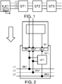
- FIG. 1 shows a schematic representation of a modular bus system according to a preferred embodiment of the invention.
- the bus system has a head module K1 and one or more base elements ST1, ST2, ST3.
- the head module K1 and the base element or the basic elements ST1, ST2, ST3 are connected via a bus system, which has at least 3 logical lines in the example shown.
- Each of the basic elements ST1, ST2, ST3 is suitable for receiving an overvoltage protection module M1, M2, M3.
- the head module K1 has a first bus connection device for contacting with a first bus potential L1, a second bus connection device for contacting with a second bus potential L2 and a third bus connection device for contacting with a signal bus L3, wherein the signal bus in a first state, the occurrence of an error and in a second state indicating the non-occurrence of an error.
- the head module K1, as in FIG. 6 shown via at least one signaling device, which indicates whether one or more errors has been signaled on the signal bus L3.
- a suitable signaling device may be, for example, a light-emitting diode LED, a display, or a sound generator SPK or the like.
- the Head module K1 also have a remote signaling device OUT, which can report a detected error.
- a telecommunication device can be, for example, a fieldbus system or another suitable interface, such as USB, Ethernet, etc. and, in a corresponding manner, the head module is set up to provide messages about the state adapted for the respective interface.
- the head module K1 can also contain an electronic processing device for evaluating, for example, 30 or more data of the overvoltage protection modules or for generating messages for transmission via the remote signaling device OUT or for display in a display.
- a microcontroller or a microprocessor can be provided for this purpose.
- connection techniques and signaling would be possible in the present invention, such as the use of other data bus systems, such as a 1-wire bus
- a particularly favorable variant is described below.
- physical properties are assigned to the three logical lines of the bus system.
- the first and second bus connection means via the first and second bus connection means a first and a second bus potential from the head module K to supply the base elements ST1, ST2, ST3 and the associated overvoltage protection modules M1, M2, M3 and the devices or systems associated with this overvoltage protection modules available provides.
- the third line, the signal bus L3 is used to signal, for example, faults in the overvoltage protection modules or incorrectly inserted overvoltage protection modules.
- the first bus potential is assigned 0 V or -12 V or a low level and the second bus potential is 3.3 V or 5 V or 12 V or a high level.
- FIG. 2 shows a schematic representation of a base element ST1 with an overvoltage protection module M1 to be plugged according to a preferred embodiment of the invention.
- the insertion direction is indicated by the arrow.
- the base element ST1, ST2, ST3 has mechanical provisions which enable a secure insertion and secure mounting of the overvoltage protection module M1, M2, M3 and enable contact by means of the bus connection devices BK1 ', BK2', BK3 '.
- This base element has a first bus connection device BK1 for contacting the first bus potential L1, a second bus connection device BK2 for contacting the second bus potential L2, and a third bus connection device BK3 for contacting the signal bus L3.
- the signal bus indicates, in a first state, the occurrence of an error, and in a second state, the absence of an error, wherein an error indicates a faulty overvoltage protection module to the head module K or head modules K, K1 and other devices connected to the bus.
- the first and second bus potential should be used to supply devices on the overvoltage protection module M1.
- the base element has an electronic monitoring device UE1, wherein the electronic monitoring device UE1 detects whether an overvoltage protection module M1 is accommodated.
- the second state is signaled via the signal bus, and in the event that no overvoltage protection module M1 is accommodated in the base element ST1 or else the overvoltage protection module M1 is recorded incorrectly, the state of the signal bus is not changed.
- an electronic monitoring device allows significantly smaller designs.
- electronic monitoring devices are inexpensive to produce and unlike mechanical switches less susceptible to interference.
- the electronic monitoring device UE1 has a semiconductor switch.
- Semiconductor switches can be manufactured and integrated particularly cost-effectively.
- the electronic monitoring device is connected as an opener, wherein in the case of a correctly recorded overvoltage protection module M1, the "switch" is opened.
- the electronic monitoring device UE1 has a transistor T1, T2.
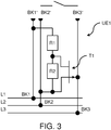
- a transistor T1, T2 Such embodiments and schematic circuits are in the Figures 3 and 4 shown. It is in FIG. 3 a base element ST1, which is connected by means of the bus connection devices BK1, BK2 to the first and second bus potential L1, L2. These bus potentials are routed to terminals BK1 ', BK2' for connection to an overvoltage protection module M1. Furthermore, the base element ST1 is connected to the signal bus L3 by means of the bus connection device BK3, which is likewise routed to a connection BK3 'for connection to the overvoltage protection module M1. Between Bus potentials is a suitably dimensioned voltage divider formed of the resistors R1 and R2 constructed.
- the first bus potential is 0 V while the second bus potential is 5 V.
- the voltage divider would then be connected to the drain of a p-channel (J) FET, for example, while the source would be connected to the first bus potential.
- the transistor T1 is conductive.
- this overvoltage protection module M1 signals that it is functioning correctly by providing a voltage or current to the signal bus L3 via the contact BK3 ', for example in which a conductive connection, shown as a make contact, is provided the contacts BK2 'and BK3', manufactures.
- the embodiment according to FIG. 4 differs only insignificantly from the embodiment in FIG. 3 , Now, a bipolar transistor is used instead of a FET transistor. Again, it is assumed that a potential of 0 V is provided on line L1 and a potential of 5 V on line L2. A resistor R3 is connected to the base of the NPN transistor T2. The emitter is connected to the second bus potential. The collector in turn is connected to the signal bus L3. In contrast to FIG. 3 the signal bus L3 is not looped through to BK3 'via BK3.
- this overvoltage protection module M1 signals that it is functioning correctly by providing a voltage or current to the signal bus L3 via the contact BK3 ', for example in which a conductive connection, shown as a make contact, is provided the contacts BK2 'and BK3', manufactures.
- the base element ST1, ST2, ST3 have a local signaling device for the optical display LED and / or for the acoustic display SPK, in order to indicate whether an overvoltage protection module M1, M2, M3 is accommodated.
- a mechanical display which for example provides a color change, may be provided to indicate whether the base element ST1 contains a correctly received overvoltage protection module.
- the signal bus can also be used for further signaling. For example, it is possible to retrieve data from individual overvoltage protection modules M1, M2, M3 and to use the signal bus L3 for the data transmission from and to the head module K, K1. For example, it is possible the state of the individual overvoltage protection modules To monitor M1, M2, M3. This data can be forwarded, for example, from the head module K, K1 via a telecommunication device OUT.
- the presented invention makes it possible to provide a bus-oriented monitoring system for overvoltage protection modules in a particularly cost-effective manner, which requires only small space, hardly demands on mechanical tolerances, is not critical to external disturbances such as shock, vibration, deposits, oxidation and also is capable of more Transport data.
- FIG. 7 Figure 4 is a schematic sectional view of a bus module and a mounting rail for use in a preferred embodiment of the invention.
- a first bus module BM1 is applied to a mounting rail TS, for example - as in the course of FIG. 7 shown - locked.
- the bus module BM1 is designed so that the first bus potential L1, the second bus potential L2 and the signal bus L3 and / or other signals can be framed by the recess of the support rail TS out. Due to the modular design can be achieved on the one hand, that the production costs are low, on the other hand, the Wiring costs are minimized, since now only the bus modules BM1, BM2 are set up. Thus, in particular for a plurality of overvoltage protection devices remote access can be realized inexpensively.
- the electronic monitoring devices UE1 can be connected to a power supply via the first and the second bus potential L1, L2. Via the signal bus L3, the monitoring devices UE1 can easily signal an error as described above.
- the wiring effort is low because the bus potentials L1, L2 and the signal bus L3 framed by the recess of the support rail TS are performed, whereby the connection is easy to produce. At the same time, the error safety is increased because the wiring is always also a source of error.
- the bus modules BM1, BM2 are designed so that they contact the first bus potential L1, the second bus potential L2 and the signal bus L3 to the base elements ST1, ST2, ST3 via the first bus connection device BK1 for contacting the first bus potential L1, the second Bus connection device BK2 for contacting with the second bus potential L2, and provide the third bus connection device BK3 for contacting with the signal bus L3.
- a bus module BM1, BM2 bus connection devices BK1, BK2, BK3, which are designed so that they can provide the respective bus potentials L1, L2, L3 a plugged head module K, K1 or a plugged base element ST1, ST2, ST3 available.
- the bus modules BM1, BM2 are preferably components of a system bus.
- the head module K, K1 be designed so that it can be latched onto a DIN rail TS.
- the head module K, K1 is designed so that it contacts the first bus potential L1, the second bus potential L2 and the signal bus L3 to the base elements ST1, ST2, ST3 via a first bus connection device BK1 for contacting the first bus potential L1, a second Bus connection device BK2 for contacting with the second bus potential L2, and a third bus connection means BK3 for contacting with the signal bus L3 provides.
- the bus module is designed so that it still allows a latching application of a head module K as well as a latching application of a base member ST1, ST2, ST3 on the mounting rail TS.
- a bus module BM1 has, as in FIG. 7 and FIG. 8 represented at least on one side in the plane of the support rail TS contacts B1, B2, B3 for contacting the bus potentials of an adjacent bus module BM2. It is particularly advantageous if the bus modules BM1, BM2 have socket-like receptacles B1, B2, B3 on the one side in the plane of the mounting rail TS, which receptacles can be brought into connection with pin-like receptacles of a second bus module BM2.
- this plug socket system provides a low cost, easy to install system bus.
- bus module BM1 snapped onto a mounting rail TS1, TS2.
- another bus module BM2 can be applied in the same way adjacent thereto.
- FIG. 8 represented by pushing together on the support rail TS1, TS2 be brought into contact with each other, whereby the bus is provided.
- a bus module BM1 can like in FIG. 9 represented a base element ST1 are applied, in turn, an overvoltage protection module M1 can be added.
- a head module K, K1 can also be applied.
- the bus system can also extend over a plurality of mounting rails TS1, TS2 as in FIG. 10 shown. It can be connected to a first bus module BM1, which is located on a first support rail TS1, by means of a cable with suitable connectors to a second bus module BM2, which is located on a second support rail TS2.
- a first bus module BM1 which is located on a first support rail TS1
- a second bus module BM2 which is located on a second support rail TS2.
- both bus modules with socket-like receptacles B1, B2, B3 on the one side and bus modules on the other side can be connected to corresponding pin-type receptacles.
- similar connectors may be provided, for example, on both sides female receptacles.
- the status polling can be implemented via remote polling without requiring additional wiring. Therefore, the solution is inexpensive and also advantageous because the bus system minimizes the risk of loose wiring.
- a faulty overvoltage protection module M1, M2, M3 can also report its status to the head station via the signal bus.
- the reported condition may include, for example, a pure defective or non-defective indication of the overvoltage protection module, or may include other gradations, such as an indication of damage requiring rapid replacement.
- gradations such as an indication of damage requiring rapid replacement.
- here are also other data, such as the number of derivatives and their duration, etc. transferable.
- a unique identifier of the overvoltage protection module M1, M2, M3 can also be provided that the respective overvoltage protection module is recognizable as sender of the display or the data.
- the display or the transmission of the data to a head station K, K1 can on the one hand via the signal bus L3, on the other hand, but also on one of the supply lines L1, L2 (eg in 1-wire technology) as well as on another, not shown Bus line done.
Landscapes
- Engineering & Computer Science (AREA)
- Physics & Mathematics (AREA)
- General Physics & Mathematics (AREA)
- Automation & Control Theory (AREA)
- Power Engineering (AREA)
- General Engineering & Computer Science (AREA)
- Emergency Protection Circuit Devices (AREA)
Description
- Die Erfindung betrifft ein Basiselement zur Aufnahme eines Überspannungsschutzmoduls als auch ein modulares Bussystem mit einem oder mehreren Basiselementen der vorgenannten Art.
- In vielen Bereichen werden heutzutage eine Vielzahl von Überspannungsschutzgeräten installiert. Dabei nimmt mit zunehmender Komplexität von Anlagen und Geräten auch das Risiko zu, dass ein fehlerhaft eingebautes Überspannungsschutzgerät zu einem Ausfall eines Gerätes oder gar zum Stillstand einer ganzen Anlage führen kann, da der Überspannungsschutz nicht gewährleistet ist.
- Um die Komplexität zu minimieren und um die Wartungsfreundlichkeit von Überspannungsschutzgeräten zu erhöhen, wurden steckbare Überspannungsschutzmodule entwickelt.
- Allerdings besteht nun das Problem zu erkennen, ob ein Überspannungsschutzmodul korrekt in einer entsprechenden Aufnahme eingesetzt ist, mit anderen Worten, ob das Überspannungsschutzmodul seine Aufgabe auch erfüllen kann. In anderen Technikbereichen, z.B. im Netzschlussbereich, wurden Systeme vorgeschlagen, bei denen ein mechanischer Tastschalter, der in ein Basiselement eingebaut ist, verwendet wird, um eine Aussage über den Steckzustand zu treffen, wie z.B. in der
DE 10 2006 038 005 A1 . Ein solches System ist beispielsweise in Produkten der Produktserie VAL-MS oder VAL-CP der Anmelderin verkörpert. - Mit zunehmender Miniaturisierung stößt dieses Prinzip jedoch an Grenzen, da die Größe der Bauteile nicht beliebig verkleinert werden kann. Zum anderen sind bei kleineren Bauformen erhöhte Anforderungen an die Fertigungstoleranzen zu stellen. Zudem nimmt die Empfindlichkeit gegenüber Schmutzablagerungen und andere mechanische Einwirkungen, wie Vibrationen oder Stoßbelastungen, stark zu. Weiterhin kann bei häufiger Betätigung der Schalter, also bei häufigem Wechsel der steckbaren Module, auch ein Verschleiß festzustellen sein, der die Schaltsicherheit minimiert. Insofern sind solche Vorrichtungen nur mit erhöhtem Design-und Kostenaufwand in kleinen Baugrößen realisierbar.
- Der Erfindung liegt die Aufgabe zu Grunde, ein modulares System für Überspannungsschutzgeräte zur Verfügung zu stellen, welches eine sichere Erkennung auch bei kleinsten Bauformen erlaubt und / oder das zudem kostengünstig herstellbar ist und / oder weiterhin auch den Verdrahtungsaufwand minimiert und zudem die Fehlersicherheit zu erhöhen.
- Die Lösung der Aufgabe erfolgt erfindungsgemäß durch die Merkmale des unabhängigen Anspruchs. Vorteilhafte Ausgestaltungen der Erfindung sind in den Unteransprüchen und der Beschreibung angegeben.
- Nachfolgend wird die Erfindung unter Bezugnahme auf die anliegende Zeichnung anhand bevorzugter Ausführungsformen näher erläutert.
- Es zeigen
- Fig. 1
- eine schematische Darstellung eines modularen Bussystems gemäß einer bevorzugten Ausführungsform der Erfindung,
- Fig. 2
- eine schematische Darstellung eines Basiselementes mit einem zu steckenden Überspannungsschutzmodul gemäß einer bevorzugten Ausführungsform der Erfindung,
- Fig. 3
- eine schematische Darstellung einer ersten Ausführungsform einer Überwachungseinrichtung in einem Basiselement gemäß einer bevorzugten Ausführungsform der Erfindung,
- Fig. 4
- eine schematische Darstellung einer zweiten Ausführungsform einer Überwachungseinrichtung in einem Basiselement gemäß einer bevorzugten Ausführungsform der Erfindung,
- Fig. 5
- eine schematische Darstellung von Elementen eines Basiselementes gemäß einer bevorzugten Ausführungsform der Erfindung,
- Fig. 6
- eine schematische Darstellung von Elementen eines Kopfmoduls gemäß einer bevorzugten Ausführungsform der Erfindung,
- Fig. 7
- eine schematische Schnittdarstellung eines Busmoduls und einer Tragschiene zur Verwendung in einer bevorzugten Ausführungsform der Erfindung,
- Fig. 8
- eine schematische Perspektivdarstellung von Busmodulen und einer Tragschiene zur Verwendung in einer bevorzugten Ausführungsform der Erfindung,
- Fig. 9
- eine schematische Schnittdarstellung eines Busmoduls und einer Tragschiene in Verwendung mit einem Überspannungsschutzmodul und einem Basiselement gemäß einer bevorzugten Ausführungsform der Erfindung,
- Fig. 10
- eine schematische Darstellung verschiedener Busverlängerungen über Tragschienen hinweg gemäß einer bevorzugten Ausführungsform der Erfindung, und
- Fig. 11
- eine schematische Darstellung einer Ausgestaltung mit zwei Kopfmodulen gemäß einer bevorzugten Ausführungsform der Erfindung.
-
Figur 1 zeigt eine schematische Darstellung eines modularen Bussystems gemäß einer bevorzugten Ausführungsform der Erfindung. Das Bussystem weist ein Kopfmodul K1 und ein oder mehrere Basiselemente ST1, ST2, ST3 auf. Das Kopfmodul K1 und das Basiselement oder die Basiselemente ST1, ST2, ST3 sind über ein Bussystem verbunden, welches im dargestellten Beispiel zumindest 3 logische Leitungen aufweist. - Jedes der Basiselemente ST1, ST2, ST3 ist zur Aufnahme eines Überspannungsschutzmoduls M1, M2, M3 geeignet. Das Kopfmodul K1 weist eine erste Busverbindungseinrichtung zur Kontaktierung mit einem ersten Buspotential L1, eine zweite Busverbindungseinrichtung zur Kontaktierung mit einem zweiten Buspotential L2 und eine dritte Busverbindungseinrichtung zur Kontaktierung mit einem Signalbus L3 auf, wobei der Signalbus in einem ersten Zustand das Auftreten eines Fehlers und in einem zweiten Zustand das Nichtauftreten eines Fehlers anzeigt. Weiterhin verfügt das Kopfmodul K1, wie in
Figur 6 gezeigt, über zumindest eine Signalisierungseinrichtung, welche anzeigt, ob auf dem Signalbus L3 ein oder mehrere Fehler signalisiert wurde. Eine geeignete Signalisierungseinrichtung kann beispielsweise eine Leuchtanzeige LED, ein Display, oder eine Tongeber SPK oder dergleichen sein. Alternativ oder zusätzlich kann das Kopfmodul K1 auch eine Fernmeldungseinrichtung OUT aufweisen, welche einen erkannten Fehler weitermelden kann. Eine solche Fernmeldeeinrichtung kann beispielsweise ein Feldbussystem oder eine andere geeignete Schnittstelle, wie z.B. USB, Ethernet, usw. sein und in entsprechender Weise ist das Kopfmodul eingerichtet, um für die jeweilige Schnittstelle angepasst Nachrichten über den Zustand bereitzustellen. Weiterhin kann das Kopfmodul K1 auch eine elektronische Verarbeitungseinrichtung zum Auswerten von z.B. 30 oder mehr Daten der Überspannungsschutzmodule bzw. zur Erstellung von Nachrichten zum Versand über die Fernmeldungseinrichtung OUT oder zur Anzeige in einem Display enthalten. Z.B. kann hierfür ein Mikrokontroller oder ein Mikroprozessor vorgesehen sein. - Obwohl andere Anschlusstechniken und Signalisierungen bei der vorgestellten Erfindung möglich wären, wie z.B. der Einsatz von anderen Datenbussystemen, z.B. einem 1-Wire-Bus, ist eine besonders günstige Variante im Folgenden beschrieben. Bei dieser Variante sind den drei logischen Leitungen des Bussystems physikalische Eigenschaften zugeordnet. So ist z.B. vorgesehen, dass über die erste und zweite Busverbindungseinrichtung ein erstes und ein zweites Buspotential seitens des Kopfmoduls K zur Versorgung der Basiselemente ST1, ST2, ST3 und diesen zugeordneten Überspannungsschutzmodulen M1, M2, M3 und der diesen Überspannungsschutzmodulen zugeordneten Geräte oder Anlagen zur Verfügung stellt. Die dritte Leitung, der Signalbus L3, wird zur Signalsierung z.B. von Fehlern der Überspannungsschutzmodule oder fehlerhaft eingeführter Überspannungsschutzmodule verwendet. Z.B. ist dem ersten Buspotential 0 V oder -12 V oder ein Low-Level und dem zweiten Buspotential 3,3 V oder 5 V oder 12 V oder ein High-Level zugeordnet.
-
Figur 2 zeigt eine schematische Darstellung eines Basiselementes ST1 mit einem zu steckenden Überspannungsschutzmodul M1 gemäß einer bevorzugten Ausführungsform der Erfindung. Dabei wird die Einführrichtung durch den Pfeil angegeben. Das Basiselement ST1, ST2, ST3 weist hierzu mechanische Vorkehrungen auf, die ein sicheres Einführen und eine sichere Halterung des Überspannungsschutzmoduls M1, M2, M3 ermöglicht und den Kontakt mittels der Busverbindungseinrichtungen BK1', BK2', BK3' ermöglichen. Dieses Basiselement weist eine erste Busverbindungseinrichtung BK1 zur Kontaktierung mit dem ersten Buspotential L1, eine zweite Busverbindungseinrichtung BK2 zur Kontaktierung mit dem zweiten Buspotential L2 und eine dritte Busverbindungseinrichtung BK3 zur Kontaktierung mit dem Signalbus L3 auf. Der Signalbus zeigt in einem ersten Zustand das Auftreten eines Fehlers und in einem zweiten Zustand das Nichtauftreten eines Fehlers an, wobei ein Fehler ein fehlendes bzw. fehlerhaft aufgenommenes Überspannungsschutzmodul dem Kopfmodul K oder den Kopfmodulen K, K1 und anderen am Bus angeschlossenen Einrichtungen anzeigt. Dabei soll das erste und zweite Buspotential zur Versorgung von Einrichtungen auf dem Überspannungsschutzmodul M1 verwendet werden. Weiterhin weist das Basiselement eine elektronische Überwachungseinrichtung UE1 auf, wobei die elektronische Überwachungseinrichtung UE1 erkennt, ob ein Überspannungsschutzmodul M1 aufgenommenen ist. Im Falle, dass ein Überspannungsschutzmodul M1 in das Basiselement ST1 aufgenommenen ist, wird der zweite Zustand über den Signalbus signalisiert, und im Falle, dass kein Überspannungsschutzmodul M1 in das Basiselement ST1 aufgenommenen ist oder aber das Überspannungsschutzmodul M1 fehlerhaft aufgenommenen ist, wird der Zustand des Signalbusses nicht verändert. - Im Unterschied zum Stand der Technik erlaubt eine elektronische Überwachungseinrichtung deutlich kleinere Bauformen. Zudem sind elektronische Überwachungseinrichtungen kostengünstig herstellbar und im Gegensatz zu mechanischen Schaltern weniger störanfällig.
- In einer vorteilhaften Weiterbildung der Erfindung weist die elektronische Überwachungseinrichtung UE1 einen Halbleiterschalter auf. Halbleiterschalter können besonders kostengünstig hergestellt und integriert werden.
- In einer weiteren, vorteilhaften Weiterbildung der Erfindung ist die elektronische Überwachungseinrichtung als ein Öffner geschaltet, wobei im Falle eines korrekt aufgenommen Überspannungsschutzmodul M1 der "Schalter" geöffnet wird.
- In einer weiteren, vorteilhaften Weiterbildung der Erfindung weist die elektronische Überwachungseinrichtung UE1 einen Transistor T1, T2 auf. Solche Ausführungsformen und schematische Beschaltungen sind in den
Figuren 3 und4 dargestellt. Dabei ist inFigur 3 ein Basiselement ST1 gezeigt, welches mittels der Busverbindungseinrichtungen BK1, BK2 mit dem ersten und zweiten Buspotential L1, L2 verbunden ist. Diese Buspotentiale sind zu Anschlüssen BK1', BK2' zur Verbindung mit einem Überspannungsschutzmodul M1 geführt. Weiterhin ist das Basiselement ST1 mit dem Signalbus L3 mittels der Busverbindungseinrichtung BK3 verbunden, die ebenfalls mit einem Anschluss BK3' zur Verbindung mit dem Überspannungsschutzmodul M1 geführt ist. Zwischen den Buspotentialen ist ein geeignet dimensionierter Spannungsteiler gebildet aus den Widerständen R1 und R2 aufgebaut. Im dargestellten Beispiel ist das erste Buspotential 0 V während das zweite Buspotential 5 V beträgt. Der Spannungsteiler würde dann z.B. mit dem Drain-Anschluss eines p-Kanal (J)FET verbunden werden, während der Source-Anschluss mit dem ersten Buspotential verbunden würde. Ist kein Überspannungsschutzmodul M1 eingeführt, d.h. sind die Kontakte BK1', BK2' und BK3' nicht kontaktiert, so ist der Transistor T1 leitend. Wird ein Überspannungsschutzmodul M1 eingeführt, so signalisiert dieses Überspannungsschutzmodul M1, dass es korrekt funktioniert, in dem es auf den Signalbus L3 über den Kontakt BK3' eine Spannung bzw. einen Strom zur Verfügung stellt, z.B. in dem eine leitende Verbindung, dargestellt als Schließer über den Kontakten BK2' und BK3', herstellt. - Die Ausführungsform gemäß
Figur 4 unterscheidet sich nur unwesentlich von der Ausführungsform inFigur 3 . Nun wird anstatt eines FET-Transistors ein Bipolartransistor verwendet. Wiederum wird angenommen, dass auf Leitung L1 ein Potential von 0 V und auf Leitung L2 ein Potential von 5 V zur Verfügung gestellt wird. Ein Widerstand R3 ist mit der Basis des npn-Transistors T2 verbunden. Der Emitter ist mit dem zweiten Buspotential verbunden. Der Kollektor wiederum ist mit dem Signalbus L3 verbunden. Im Unterschied zuFigur 3 ist der Signalbus L3 über BK3 nicht zu Anschluss BK3' durchgeschleift. Wird ein Überspannungsschutzmodul M1 eingeführt, so signalisiert dieses Überspannungsschutzmodul M1, dass es korrekt funktioniert, in dem es auf den Signalbus L3 über den Kontakt BK3' eine Spannung bzw. einen Strom zur Verfügung stellt, z.B. in dem eine leitende Verbindung, dargestellt als Schließer über den Kontakten BK2' und BK3', herstellt. - Natürlich können auch andere Halbleiterelemente und Schaltungen verwendet werden. Wesentlich an den Schaltungen für UE1 ist, dass ein fehlerhafter Überspannungsschutz eines einzelnen Moduls zu einer Fehlermeldung im Kopfmodul führt.
- Weiterhin kann in vorteilhaften Weiterbildungen der Erfindung, wie in
Figur 5 gezeigt, das Basiselement ST1, ST2, ST3 eine lokale Signalisierungseinrichtung zur optischen Anzeige LED und / oder zur akustischen Anzeige SPK aufweisen, um anzuzeigen, ob ein Überspannungsschutzmodul M1, M2, M3 aufgenommen ist. Dabei kann alternativ oder zusätzlich auch eine mechanische Anzeige, welche z.B. einen Farbwechsel bereitstellt, vorgesehen sein, um anzuzeigen, ob das Basiselement ST1 ein korrekt aufgenommenes Überspannungsschutzmodul enthält. - Durch die zuvor beschriebene Ausgestaltung mit einer Öffnerfunktion wird das fehlerhafte Aufnehmen eines einzelnen Überspannungsschutzmoduls auf dem Signalbus nicht durch weitere korrekt aufgenommene Überspannungsschutzmodule gestört. Somit wird im logischen Sinne eine Oder-Funktion realisiert und der Kopfstation der Fehler eines oder mehrerer Überspannungsschutzmodule auf dem von ihm überwachten Bus mitgeteilt.
- Befinden sich alle Überspannungsschutzmodule in den jeweiligen Aufnahmen, kann der Signalbus auch für weitere Signalisierungen verwendet werden. So ist es z.B. möglich Daten von einzelnen Überspannungsschutzmodulen M1, M2, M3 abzurufen und den Signalbus L3 für die Datenübertragung von und zum Kopfmodul K, K1 zu verwenden. So ist es z.B. möglich den Zustand der einzelnen Überspannungsschutzmodule M1, M2, M3 zu überwachen. Diese Daten können z.B. vom Kopfmodul K, K1 über eine Fernmeldeeinrichtung OUT weitergeleitet werden.
- Weiterhin ist es möglich, dass ein Fehler des Überspannungsschutzmoduls M1, M2, M3 auch mittelbar über das Basiselement erfolgt, z.B. in dem die zuvor beschriebene Schließerfunktion aufgehoben wird und somit faktisch der gleiche Fehler wie ein nicht gestecktes Überspannungsschutzmodul signalisiert wird.
- Die vorgestellte Erfindung erlaubt es in besonders kostengünstiger Weise ein busorientiertes Überwachungssystem für Überspannungsschutzmodule bereitzustellen, welches lediglich geringen Bauraum erfordert, kaum Anforderungen an mechanische Toleranzen stellt, unkritisch gegenüber äußeren Störeinflüssen wie Stoß, Vibration, Ablagerungen, Oxidation ist und zudem auch in der Lage ist weitere Daten zu transportieren.
- In
Figur 7 ist eine schematische Schnittdarstellung eines Busmoduls und einer Tragschiene zur Verwendung in einer bevorzugten Ausführungsform der Erfindung gezeigt. - Dabei wird auf eine Tragschiene TS ein erstes Busmodul BM1 aufgebracht, z.B. - wie im Ablauf der
Figur 7 dargestellt - aufgerastet. - Das Busmodul BM1 ist dabei so gestaltet, dass das erste Buspotential L1, das zweite Buspotential L2 und der Signalbus L3 und / oder weitere Signale umrahmt von der Vertiefung der Tragschiene TS geführt werden können. Durch die modulare Gestaltung kann zum einen erreicht werden, dass die Fertigungskosten gering sind, zum anderen kann der Verdrahtungsaufwand minimiert werden, da nun lediglich die Busmodule BM1, BM2 aufzusetzen sind. Somit kann insbesondere für eine Mehrzahl Überspannungsschutzeinrichtungen eine Fernabfrage kostengünstig realisiert werden. Die elektronischen Überwachungseinrichtungen UE1 können über das erste und das zweite Buspotential L1, L2 mit einer Energieversorgung verbunden werden. Über den Signalbus L3 können die Überwachungseinrichtungen UE1 einen Fehler wie zuvor beschrieben einfach signalisieren. Der Verdrahtungsaufwand ist gering, da die Buspotentiale L1, L2 und der Signalbus L3 umrahmt von der Vertiefung der Tragschiene TS geführt werden, wodurch die Verbindung leicht herstellbar ist. Gleichzeitig wird die Fehlersicherheit erhöht, da die Verdrahtung immer auch eine Fehlerquelle darstellt.
- Die Busmodule BM1, BM2 sind dabei so gestaltet, dass sie den Kontakt des ersten Buspotentials L1, des zweiten Buspotentials L2 und des Signalbusses L3 zu den Basiselementen ST1, ST2, ST3 über die erste Busverbindungseinrichtung BK1 zur Kontaktierung mit dem ersten Buspotential L1, die zweite Busverbindungseinrichtung BK2 zur Kontaktierung mit dem zweiten Buspotential L2, und die dritte Busverbindungseinrichtung BK3 zur Kontaktierung mit dem Signalbus L3 zur Verfügung stellen.
- Dazu weist ein Busmodul BM1, BM2 Busverbindungseinrichtungen BK1, BK2, BK3 auf, die so gestaltet sind, dass sie die jeweiligen Buspotentiale L1, L2, L3 einem aufgesteckten Kopfmodul K, K1 oder einen aufgesteckten Basiselement ST1, ST2, ST3 zur Verfügung stellen können.
- Bevorzugt sind die Busmodule BM1, BM2 Bestandteile eines Systembusses.
- Weiterhin kann auch das Kopfmodul K, K1 so gestaltet sein, dass es auf eine Tragschiene TS aufrastbar ist.
- Das Kopfmodul K, K1 ist dabei so gestaltet, dass es den Kontakt des ersten Buspotentials L1, des zweiten Buspotentials L2 und des Signalbusses L3 zu den Basiselementen ST1, ST2, ST3 über eine erste Busverbindungseinrichtung BK1 zur Kontaktierung mit dem ersten Buspotential L1, eine zweite Busverbindungseinrichtung BK2 zur Kontaktierung mit dem zweiten Buspotential L2, und eine dritte Busverbindungseinrichtung BK3 zur Kontaktierung mit dem Signalbus L3 zur Verfügung stellt.
- Weiterhin ist das Busmodul so gestaltet, dass es dennoch eine rastende Aufbringung eines Kopfmoduls K als auch eine rastende Aufbringung eines Basiselementes ST1, ST2, ST3 auf die Tragschiene TS erlaubt.
- Ein Busmodul BM1 weist wie in
Figur 7 und Figur 8 dargestellt zumindest auf einer Seite in der Ebene der Tragschiene TS Kontakte B1, B2, B3 zur Kontaktierung der Buspotentiale eines benachbarten Busmoduls BM2 auf. Besonders vorteilhaft ist es, wenn die Busmodule BM1, BM2 auf der einen Seite in der Ebene der Tragschiene TS buchsenartige Aufnahmen B1, B2, B3 aufweist, welche mit stiftartigen Aufnahmen eines zweiten Busmoduls BM2 in Verbindung gebracht werden können. - Offensichtlich kann durch dieses Stecker-Steckdosensystem ein kostengünstiger, einfach zu montierender Systembus zur Verfügung gestellt werden.
- Bei der Montage wird zunächst wie in
Figur 7 dargestellt ein Busmodul BM1 auf eine Tragschiene TS1, TS2 aufgerastet. Anschließend kann in gleicher Weise benachbart hierzu ein weiteres Busmodul BM2 aufgebracht werden. Diese können dann wie inFigur 8 dargestellt durch zusammenschieben auf der Tragschiene TS1, TS2 in Kontakt zueinander gebracht werden, wodurch der Bus zur Verfügung gestellt wird. Auf ein Busmodul BM1 kann wie inFigur 9 dargestellt eine Basiselement ST1 aufgebracht werden, in dem wiederum ein Überspannungsschutzmodul M1 aufgenommen werden kann. Alternativ zum Basiselement ST1 kann auch ein Kopfmodul K, K1 aufgebracht werden. - Das Bussystem kann sich auch über mehrere Tragschienen TS1, TS2 erstrecken wie in
Figur 10 gezeigt. Dabei kann an ein erstes Busmodul BM1, welches sich auf einer ersten Tragschiene TS1 befindet, mittels eines Kabels mit geeigneten Steckverbindern an ein zweites Busmodul BM2, welches sich auf einer zweiten Tragschiene TS2 befindet, verbunden sein. Durch geeignete Ausgestaltung der Steckverbinder können sowohl Busmodule mit buchsenartige Aufnahmen B1, B2, B3 auf der einen Seite und Busmodule auf der anderen Seite mit entsprechenden stiftartigen Aufnahmen verbunden werden. Andererseits können auch gleichartige Steckverbinder vorgesehen sein, z.B. auf beiden Seiten buchsenartige Aufnahmen. - Weiterhin, sollte die Leistung eines Kopfmoduls K nicht ausreichend sein, könnte auch - wie in
Figur 11 gezeigt - ein weiteres Kopfmodul K1 eingesetzt werden, dass die elektrische Leistung für weitere Module zur Verfügung stellt. Dabei bewirkt die Ausgestaltung des Bussystems das ein Fehler eines Überspannungsschutzmoduls M2, welches vermittels eines Busmoduls BM2 angeschlossen ist und welches sich logisch hinter dem zweiten Kopfmodul K1 befindet, von beiden Kopfmodulen K, K1 als Fehler angezeigt wird. Umgekehrt wird auch ein Fehler eines Überspannungsschutzmoduls M1, welches vermittels eines Busmoduls BM1 angeschlossen ist und welches sich logisch hinter der ersten Kopfstation K und vor dem zweiten Kopfmodul K1 befindet, von beiden Kopfmodulen K, K1 als Fehler angezeigt wird. D.h. der Bus kann so um eine Anzahl weiterer Module erweitert werden. Weiterhin ist es natürlich möglich auch mehr als zwei Kopfmodule einzusetzen. - Werden nun viele Überspannungsschutzeinrichtungen benötigt, kann die Zustandsabfrage über eine Fernabfrage realisiert werden, ohne einen zusätzlichen Verdrahtungsaufwand zu erfordern. Daher ist die Lösung kostengünstig und zudem vorteilhaft, da das Bussystem die Gefahr gelöster Verdrahtung minimiert.
- Ein fehlerhaftes Überspannungsschutzmodul M1, M2, M3 kann zudem über den Signalbus seinen Zustand an die Kopfstation melden. Dabei kann der gemeldete Zustand zum Beispiel eine reine defekt oder nicht-defekt Anzeige des Überspannungsschutzmoduls beinhalten oder aber weitere Abstufungen enthalten, wie z.B. eine Anzeige einer Schädigung, die ein baldiges Auswechseln erfordert. Natürlich sind hier auch weitere Daten, wie z.B. die Anzahl der erfolgten Ableitungen und deren Dauer etc. übertragbar. Weiterhin kann auch eine eindeutige Kennung des Überspannungsschutzmoduls M1, M2, M3 vorgesehen sein, so dass das jeweilige Überspannungsschutzmodul als Absender der Anzeige bzw. der Daten erkennbar ist. Die Anzeige bzw. die Übermittlung der Daten zu einer Kopfstation K, K1 kann dabei zum einen über den Signalbus L3, zum anderen aber auch auf einer der Versorgungsleitungen L1, L2 (z.B. in 1-Wire Technik) als auch auf einer weiteren, nicht dargestellten Busleitung erfolgen.
Bezugszeichenliste Basiselement ST1, ST2, ST3 Überspannungsschutzmodul M1, M2, M3 erste Busverbindungseinrichtung BK1, BK1' zweite Busverbindungseinrichtung BK2, BK2' dritte Busverbindungseinrichtung BK3, BK3' elektronische Überwachungseinrichtung UE1 Kopfmodul K, K1 Widerstand R1, R2, R3, R4 Transistor T1, T2 Optische Signalisierungseinrichtung LED Akustische Signalisierungseinrichtung SPK Erstes Buspotential, Leitung L1 Zweites Buspotential, Leitung L2 Signalbus, Leitung L3 Tragschiene TS1, TS2 Busmodul BM1, BM2 Kontakte B1, B2, B3 Fernmeldungseinrichtung OUT
Claims (18)
- Basiselement (ST1, ST2, ST3) zur Aufnahme eines Überspannungsschutzmoduls (M1, M2, M3) zur Verwendung in einem Bussystem, aufweisend• eine erste Busverbindungseinrichtung (BK1) zur Kontaktierung mit einem ersten Buspotential (L1),• eine zweite Busverbindungseinrichtung (BK2) zur Kontaktierung mit einem zweiten Buspotential (L2),• eine dritte Busverbindungseinrichtung (BK3) zur Kontaktierung mit einem Signalbus (L3), wobei der Signalbus in einem ersten Zustand das Auftreten eines Fehlers und in einem zweiten Zustand das Nichtauftreten eines Fehlers anzeigt,• wobei ein Fehler ein fehlendes bzw. fehlerhaft aufgenommenes bzw. fehlerbehaftetes Überspannungsschutzmodul (M1, M2, M3) anzeigt,• wobei das erste und zweite Buspotential zur Versorgung von Einrichtungen auf dem Überspannungsschutzmodul (M1, M2, M3) verwendet werden soll,• dadurch gekennzeichnet, dass das Basiselement weiterhin eine elektronische Überwachungseinrichtung (UE1) aufweist, wobei die elektronische Überwachungseinrichtung (UE1) erkennt, ob ein Überspannungsschutzmodul (M1, M2, M3) aufgenommenen ist, und wobei• im Falle dass ein Überspannungsschutzmodul (M1, M2, M3) in das Basiselement (ST1, ST2, ST3) aufgenommenen ist, der zweite Zustand über den Signalbus signalisiert wird, und• im Falle dass kein Überspannungsschutzmodul (M1, M2, M3) in das Basiselement (ST1, ST2, ST3) aufgenommenen ist oder aber das Überspannungsschutzmodul (M1, M2, M3) fehlerhaft aufgenommenen ist oder das Überspannungsschutzmodul (M1, M2, M3) fehlerbehaftet ist, zeigt der Signalbus den ersten Zustand.
- Basiselement nach Anspruch 1, dadurch gekennzeichnet, dass die Basiselemente (ST1, ST2, ST3) auf eine Tragschiene (TS1, TS2) aufrastbar sind und das erste Buspotential (L1), das zweite Buspotential (L2) und der Signalbus (L3) in einer Vertiefung der Tragschiene (TS1, TS2) geführt werden.
- Basiselement nach Anspruch 1 oder 2, dadurch gekennzeichnet, dass die elektronische Überwachungseinrichtung einen Halbleiterschalter aufweist.
- Basiselement nach einem der vorhergehenden Ansprüche, dadurch gekennzeichnet, dass die elektronische Überwachungseinrichtung ein Öffner ist, wobei im Falle eines korrekt aufgenommenen Überspannungsschutzmoduls (M1) der Schalter geöffnet wird.
- Basiselement nach einem der vorhergehenden Ansprüche, dadurch gekennzeichnet, dass die elektronische Überwachungseinrichtung einen Transistor aufweist.
- Basiselement nach einem der vorhergehenden Ansprüche, dadurch gekennzeichnet, dass die elektronische Überwachungseinrichtung einen FET und / oder einen Bipolar Transistor aufweist.
- Basiselement nach einem der vorhergehenden Ansprüche weiterhin aufweisend eine lokale Signalisierungseinrichtung zur optischen und / oder akustischen Anzeige, ob ein Überspannungsschutzmodul korrekt aufgenommen ist.
- Basiselement nach einem der vorhergehenden Ansprüche, dadurch gekennzeichnet, dass die Buspotentiale mittels eines Systembusses zur Verfügung gestellt werden.
- Modulares Bussystem mit• einem oder mehreren Basiselementen (ST1, ST2, ST3) zur Aufnahme eines Überspannungsschutzmoduls (M1, M2, M3) gemäß einem der vorhergehenden Ansprüche und• einem Kopfmodul (K1, K2) aufweisend:▪ eine erste Busverbindungseinrichtung zur Kontaktierung mit einem ersten Buspotential,▪ eine zweite Busverbindungseinrichtung zur Kontaktierung mit einem zweiten Buspotential,▪ eine dritte Busverbindungseinrichtung zur Kontaktierung mit einem Signalbus, wobei der Signalbus in einem ersten Zustand das Auftreten eines Fehlers und in einem zweiten Zustand das Nichtauftreten eines Fehlers anzeigt,▪ eine Signalisierungseinrichtung, welche anzeigt, ob auf dem Signalbus ein Fehler signalisiert wurde, wobei das Kopfmodul (K1, K2) auf eine Tragschiene (TS1, TS2) aufrastbar ist und das erste Buspotential (L1), das zweite Buspotential (L2) und der Signalbus (L3) in einer Vertiefung der Tragschiene (TS1, TS2) geführt wird.
- Modulares Bussystem gemäß Anspruch 9, dadurch gekennzeichnet, dass das Kopfmodul (K1, K2) weiterhin eine Fernmeldungseinrichtung (OUT) aufweist, welche einen erkannten Fehler weitermelden kann.
- Modulares Bussystem gemäß Anspruch 9 oder 10, dadurch gekennzeichnet, dass das Kopfmodul (K1, K2) über die erste und zweite Busverbindungseinrichtung ein erstes und ein zweites Buspotential zur Versorgung der Basiselemente zur Verfügung stellt
- Modulares Bussystem nach einem der vorhergehenden Ansprüche 9 bis 11, dadurch gekennzeichnet, dass die Buspotentiale mittels eines Systembusses zur Verfügung gestellt werden.
- Modulares Bussystem nach Anspruch 12, dadurch gekennzeichnet, dass der Systembus ein oder mehrere Busmodule (BM1, BM2) aufweist, wobei ein Busmodul auf eine Tragschiene (TS1, TS2) aufrastbar ist, und ein Busmodul (BM1, BM2) Busverbindungseinrichtungen (BK1, BK2, BK3) aufweist, die so gestaltet sind, dass sie die jeweiligen Buspotentiale (L1, L2, L3) einem aufgesteckten Kopfmodul (K1, K2) oder einen aufgesteckten Basiselement (ST1, ST2, ST3) zur Verfügung stellen können.
- Modulares Bussystem nach einem der vorhergehenden Ansprüche 12 oder 13, dadurch gekennzeichnet, dass das Busmodul (BM1) zumindest auf einer Seite in der Ebene der Tragschiene (TS1, TS2) Kontakte (B1, B2, B3) zur Kontaktierung der Buspotentiale eines benachbarten Busmoduls (BM2) zur Verfügung stellt.
- Modulares Bussystem nach einem der vorhergehenden Ansprüche 12 bis 14, dadurch gekennzeichnet, dass zumindest ein Teil der Busverbindungseinrichtungen (BK1, BK2, BK3) so gestaltet sind, dass sie eine oder mehrere buchsenartige Aufnahmen (B1, B2, B3) aufweisen, welche mit stiftartigen Aufnahmen in Verbindung gebracht werden können.
- Modulares Bussystem nach einem der vorhergehenden Ansprüche 12 bis 15, dadurch gekennzeichnet, dass zumindest ein Teil der Busverbindungseinrichtungen (BK1, BK2, BK3) so gestaltet sind, dass sie eine oder mehrere stiftartige Aufnahmen aufweisen, welche mit buchsenartigen Aufnahmen (B1, B2, B3) in Verbindung gebracht werden können.
- Modulares Bussystem nach einem der vorhergehenden Ansprüche 12 bis 16, dadurch gekennzeichnet, dass der Systembus über zwei oder mehr Kopfmodule (K, K1) verfügt.
- Modulares Bussystem nach einem der vorhergehenden Ansprüche 12 bis 17, dadurch gekennzeichnet, dass der Systembus sich über zwei oder mehr Tragschienen (TS1, TS2) erstreckt.
Applications Claiming Priority (3)
| Application Number | Priority Date | Filing Date | Title |
|---|---|---|---|
| DE102011052803A DE102011052803A1 (de) | 2011-08-18 | 2011-08-18 | Basiselement zur Aufnahme eines Überspannungsschutzmoduls |
| DE202012002282U DE202012002282U1 (de) | 2011-08-18 | 2012-03-08 | Basiselement zur Aufnahme eines Überspannungsschutzmoduls |
| PCT/EP2012/066079 WO2013024151A1 (de) | 2011-08-18 | 2012-08-17 | Basiselement zur aufnahme eines überspannungsschutzmoduls und modulares bussystem |
Publications (2)
| Publication Number | Publication Date |
|---|---|
| EP2745179A1 EP2745179A1 (de) | 2014-06-25 |
| EP2745179B1 true EP2745179B1 (de) | 2017-10-04 |
Family
ID=45999380
Family Applications (1)
| Application Number | Title | Priority Date | Filing Date |
|---|---|---|---|
| EP12750746.5A Active EP2745179B1 (de) | 2011-08-18 | 2012-08-17 | Basiselement zur aufnahme eines überspannungsschutzmoduls und modulares bussystem |
Country Status (5)
| Country | Link |
|---|---|
| US (1) | US9482716B2 (de) |
| EP (1) | EP2745179B1 (de) |
| CN (1) | CN103748525B (de) |
| DE (2) | DE102011052803A1 (de) |
| WO (1) | WO2013024151A1 (de) |
Families Citing this family (8)
| Publication number | Priority date | Publication date | Assignee | Title |
|---|---|---|---|---|
| DE102011052803A1 (de) * | 2011-08-18 | 2013-02-21 | Phoenix Contact Gmbh & Co. Kg | Basiselement zur Aufnahme eines Überspannungsschutzmoduls |
| DE102014218646B4 (de) | 2013-09-18 | 2025-11-06 | Phoenix Contact Gmbh & Co. Kg | Steckbare aktive Elemente in Querrichtung für Reihenklemmensysteme mit Kodiersystem |
| DE102014103575B4 (de) | 2014-03-17 | 2024-06-27 | OBO Bettermann Hungary Kft. | Vorrichtung zum Schutz gegen Überspannungen |
| DE102014004241A1 (de) * | 2014-03-25 | 2015-10-01 | Matthias Madlehn | l/O-Modulsystem mit l/O-Modulen und Modulbrücke |
| US9807846B1 (en) | 2015-12-04 | 2017-10-31 | General Electric Company | Protection circuit assembly and method |
| CN112805890B (zh) | 2018-08-07 | 2022-03-22 | 欧宝贝特曼匈牙利有限公司 | 用于保护数据线路以防过压的装置 |
| NL2022357B1 (en) * | 2019-01-09 | 2020-08-13 | Schreder Sa | Luminaire system with spd |
| TWI693414B (zh) * | 2019-09-10 | 2020-05-11 | 矽品精密工業股份有限公司 | 檢測設備及其測試裝置 |
Family Cites Families (27)
| Publication number | Priority date | Publication date | Assignee | Title |
|---|---|---|---|---|
| US4484185A (en) * | 1983-08-12 | 1984-11-20 | Graves James D | Safety plug adapter |
| US6000825A (en) * | 1994-08-11 | 1999-12-14 | Fredriksson; Lars-Berno | Method and arrangement for a module which can be connected to a serial and digital network system |
| US6217389B1 (en) * | 1999-02-08 | 2001-04-17 | Amphenol Corporation | Universal serial bus connector with an integral over-current protection device and indicator |
| JP2005535110A (ja) * | 2002-06-25 | 2005-11-17 | タイコ・エレクトロニクス・コーポレイション | データバスインターフェースに過電流及び過電圧の保護とコモンモードフィルタリングを与える集積化デバイス |
| TWM270522U (en) * | 2004-01-02 | 2005-07-11 | Shang-Lung Huang | Safety socket structure with over-heat and over-current protection function |
| DE102004009072A1 (de) * | 2004-02-23 | 2005-09-08 | Phoenix Contact Gmbh & Co. Kg | Überspannungsschutzelement und Zündelement für ein Überspannungsschutzelement |
| TWM270539U (en) * | 2004-03-05 | 2005-07-11 | Shang-Lung Huang | Safety adapting socket structure |
| DE202004006227U1 (de) * | 2004-04-16 | 2004-09-16 | Phoenix Contact Gmbh & Co. Kg | Überspannungsschutzgerät |
| JP4429987B2 (ja) * | 2005-07-29 | 2010-03-10 | 株式会社ジェイテクト | 安全plc |
| CN2840399Y (zh) * | 2005-09-30 | 2006-11-22 | 富士康(昆山)电脑接插件有限公司 | 电连接器 |
| DE202006006659U1 (de) * | 2006-04-21 | 2006-07-06 | Phoenix Contact Gmbh & Co. Kg | Elektrisches oder elektronisches Gerät |
| DE102006038005B4 (de) * | 2006-05-22 | 2009-04-23 | Dehn + Söhne Gmbh + Co. Kg | Anschluss- und Basisteil zur Aufnahme eines steckbaren Überspannungsableiters |
| DE102006030570B4 (de) * | 2006-07-03 | 2009-09-17 | Dehn + Söhne Gmbh + Co. Kg | Basisteil zur elektrischen und mechanischen Aufnahme mindestens eines in das Basisteil einsteckbaren Überspannungsableiters |
| DE102006044344A1 (de) * | 2006-09-18 | 2008-03-27 | Phoenix Contact Gmbh & Co. Kg | Überspannungsschutzgerät |
| US7497737B2 (en) * | 2006-10-19 | 2009-03-03 | Tyco Electronics Corporation | Subminiature electrical connector including over-voltage and over-current circuit protection |
| CN101622765A (zh) * | 2006-12-29 | 2010-01-06 | 菲尼克斯电气公司 | 用于电子设备的电压保护装置 |
| JP5139145B2 (ja) * | 2008-05-09 | 2013-02-06 | タイコエレクトロニクスジャパン合同会社 | 電気コネクタ |
| DE102008025936A1 (de) | 2008-05-29 | 2009-12-03 | Phoenix Contact Gmbh & Co. Kg | Überspannungsschutzgerät |
| DE102008063816A1 (de) * | 2008-12-19 | 2010-06-24 | Wago Verwaltungsgesellschaft Mbh | Schutzeinrichtung |
| DE102009004673A1 (de) * | 2009-01-12 | 2010-07-15 | Phoenix Contact Gmbh & Co. Kg | Überspannungsschutzelement |
| DE102009015068A1 (de) * | 2009-03-26 | 2010-10-07 | Abb Ag | Überspannungsschutz für ein Busgerät |
| DE102009035060A1 (de) * | 2009-07-28 | 2011-02-03 | Phoenix Contact Gmbh & Co. Kg | Überspannungschutzelement |
| DE102009036125A1 (de) * | 2009-08-05 | 2011-02-10 | Phoenix Contact Gmbh & Co. Kg | Überspannungsschutzelement |
| US8982578B2 (en) * | 2010-10-14 | 2015-03-17 | Tyco Electronics Corporation | Connector system and assembly having integrated protection circuitry |
| KR101754111B1 (ko) * | 2011-01-03 | 2017-07-06 | 페어차일드코리아반도체 주식회사 | 적응형 과전압 보호 회로 및 방법, 및 이를 포함하는 전력 시스템 |
| SI23749A (sl) * | 2011-05-11 | 2012-11-30 | ISKRA@ZAŠČITE@d@o@o | Redudančni prenapetostni odklopnik z rotacijskimdiskom in z dodanim elektronskim sklopom za zagotavljanje podaljšanja življenjske dobe prenapetostnega gradnika |
| DE102011052803A1 (de) * | 2011-08-18 | 2013-02-21 | Phoenix Contact Gmbh & Co. Kg | Basiselement zur Aufnahme eines Überspannungsschutzmoduls |
-
2011
- 2011-08-18 DE DE102011052803A patent/DE102011052803A1/de not_active Withdrawn
-
2012
- 2012-03-08 DE DE202012002282U patent/DE202012002282U1/de not_active Expired - Lifetime
- 2012-08-17 US US14/239,536 patent/US9482716B2/en active Active
- 2012-08-17 EP EP12750746.5A patent/EP2745179B1/de active Active
- 2012-08-17 WO PCT/EP2012/066079 patent/WO2013024151A1/de not_active Ceased
- 2012-08-17 CN CN201280040215.5A patent/CN103748525B/zh active Active
Non-Patent Citations (1)
| Title |
|---|
| None * |
Also Published As
| Publication number | Publication date |
|---|---|
| DE202012002282U1 (de) | 2012-03-28 |
| US9482716B2 (en) | 2016-11-01 |
| WO2013024151A1 (de) | 2013-02-21 |
| CN103748525A (zh) | 2014-04-23 |
| CN103748525B (zh) | 2015-10-14 |
| EP2745179A1 (de) | 2014-06-25 |
| DE102011052803A1 (de) | 2013-02-21 |
| US20140253164A1 (en) | 2014-09-11 |
Similar Documents
| Publication | Publication Date | Title |
|---|---|---|
| DE202012002282U1 (de) | Basiselement zur Aufnahme eines Überspannungsschutzmoduls | |
| DE102016111690B4 (de) | Stromverteiler für ein Fahrzeug | |
| EP1353412B1 (de) | Modularer Steckverbinder | |
| DE112010001587B4 (de) | Kommunikationsadressen-Erfassungsvorrichtung, Stecker mit eingebauter Steuerschaltung und Kommunikationsadressen-Erfassungsverfahren | |
| DE112008000981T5 (de) | Systeme und Verfahren zum Indentifizieren von Steckerleitungsverbindungen in einem Kommunikations-Steckersystem unter Verwendung von einer Gleichtakt-Übertragung | |
| EP4200944B1 (de) | Elektrischer steckverbinder | |
| DE102011050638A1 (de) | Konnektor | |
| DE102020101085A1 (de) | Vorrichtung zum Verarbeiten von Signalen zwischen einer Steuerung und Feldgeräten | |
| EP3799669B1 (de) | Vorrichtung zum schutz von datenleitungen gegen überspannungen | |
| DE102012003345A1 (de) | Anordnung zur Überwachung einer Photovoltaikanlage | |
| DE202020005817U1 (de) | Elektrischer Steckverbinder | |
| DE102011076377A1 (de) | Elektrische Reihenklemmenanordnung | |
| EP1236306B1 (de) | Bussystem | |
| DE102008045337B4 (de) | Verteileranschlussmodul | |
| DE102015100843A1 (de) | Kontaktzustand-Überwachungsvorrichtung zur Überwachung von Kontaktzuständen eines Konnektors | |
| EP3240133B1 (de) | Busteilnehmer | |
| DE202015101777U1 (de) | Steckermodul für einen modularen Steckverbinder | |
| DE2347191A1 (de) | Anordnung zur ueberwachung von durch entriegelungen und/oder spannungsausfaelle bedingten stoerungen an steckbaren baugruppen | |
| EP3435275B1 (de) | Überwachungsvorrichtung | |
| DE202018100482U1 (de) | Überspannungsschutzensemble | |
| DE20203787U1 (de) | Testgerät für ISDN-S.-Bussysteme zur Überprüfung der Kontaktbelegung und der Datenaktivität | |
| LU93258B1 (de) | Sammelfernmeldevorrichtung | |
| DE102024133484A1 (de) | Ladesteckverbinder und verfahren zur überwachung eines ladesteckverbinders | |
| DE102018117896A1 (de) | Netzwerkvorrichtung zur Sicherung der Verfügbarkeit eines Netzwerkgerätes | |
| EP1273924B1 (de) | Vorrichtung zur Erkennung elektrisch leitfähiger Verunreinigungen auf der Anschlussseite eines elektrischen Verbinders |
Legal Events
| Date | Code | Title | Description |
|---|---|---|---|
| PUAI | Public reference made under article 153(3) epc to a published international application that has entered the european phase |
Free format text: ORIGINAL CODE: 0009012 |
|
| 17P | Request for examination filed |
Effective date: 20140218 |
|
| AK | Designated contracting states |
Kind code of ref document: A1 Designated state(s): AL AT BE BG CH CY CZ DE DK EE ES FI FR GB GR HR HU IE IS IT LI LT LU LV MC MK MT NL NO PL PT RO RS SE SI SK SM TR |
|
| DAX | Request for extension of the european patent (deleted) | ||
| GRAP | Despatch of communication of intention to grant a patent |
Free format text: ORIGINAL CODE: EPIDOSNIGR1 |
|
| STAA | Information on the status of an ep patent application or granted ep patent |
Free format text: STATUS: GRANT OF PATENT IS INTENDED |
|
| INTG | Intention to grant announced |
Effective date: 20170406 |
|
| GRAS | Grant fee paid |
Free format text: ORIGINAL CODE: EPIDOSNIGR3 |
|
| GRAA | (expected) grant |
Free format text: ORIGINAL CODE: 0009210 |
|
| STAA | Information on the status of an ep patent application or granted ep patent |
Free format text: STATUS: THE PATENT HAS BEEN GRANTED |
|
| AK | Designated contracting states |
Kind code of ref document: B1 Designated state(s): AL AT BE BG CH CY CZ DE DK EE ES FI FR GB GR HR HU IE IS IT LI LT LU LV MC MK MT NL NO PL PT RO RS SE SI SK SM TR |
|
| REG | Reference to a national code |
Ref country code: GB Ref legal event code: FG4D Free format text: NOT ENGLISH |
|
| REG | Reference to a national code |
Ref country code: CH Ref legal event code: EP |
|
| REG | Reference to a national code |
Ref country code: AT Ref legal event code: REF Ref document number: 934586 Country of ref document: AT Kind code of ref document: T Effective date: 20171015 |
|
| REG | Reference to a national code |
Ref country code: IE Ref legal event code: FG4D Free format text: LANGUAGE OF EP DOCUMENT: GERMAN |
|
| REG | Reference to a national code |
Ref country code: DE Ref legal event code: R096 Ref document number: 502012011401 Country of ref document: DE |
|
| REG | Reference to a national code |
Ref country code: NL Ref legal event code: MP Effective date: 20171004 |
|
| REG | Reference to a national code |
Ref country code: LT Ref legal event code: MG4D |
|
| PG25 | Lapsed in a contracting state [announced via postgrant information from national office to epo] |
Ref country code: NL Free format text: LAPSE BECAUSE OF FAILURE TO SUBMIT A TRANSLATION OF THE DESCRIPTION OR TO PAY THE FEE WITHIN THE PRESCRIBED TIME-LIMIT Effective date: 20171004 |
|
| PG25 | Lapsed in a contracting state [announced via postgrant information from national office to epo] |
Ref country code: SE Free format text: LAPSE BECAUSE OF FAILURE TO SUBMIT A TRANSLATION OF THE DESCRIPTION OR TO PAY THE FEE WITHIN THE PRESCRIBED TIME-LIMIT Effective date: 20171004 Ref country code: ES Free format text: LAPSE BECAUSE OF FAILURE TO SUBMIT A TRANSLATION OF THE DESCRIPTION OR TO PAY THE FEE WITHIN THE PRESCRIBED TIME-LIMIT Effective date: 20171004 Ref country code: FI Free format text: LAPSE BECAUSE OF FAILURE TO SUBMIT A TRANSLATION OF THE DESCRIPTION OR TO PAY THE FEE WITHIN THE PRESCRIBED TIME-LIMIT Effective date: 20171004 Ref country code: NO Free format text: LAPSE BECAUSE OF FAILURE TO SUBMIT A TRANSLATION OF THE DESCRIPTION OR TO PAY THE FEE WITHIN THE PRESCRIBED TIME-LIMIT Effective date: 20180104 Ref country code: LT Free format text: LAPSE BECAUSE OF FAILURE TO SUBMIT A TRANSLATION OF THE DESCRIPTION OR TO PAY THE FEE WITHIN THE PRESCRIBED TIME-LIMIT Effective date: 20171004 |
|
| PG25 | Lapsed in a contracting state [announced via postgrant information from national office to epo] |
Ref country code: HR Free format text: LAPSE BECAUSE OF FAILURE TO SUBMIT A TRANSLATION OF THE DESCRIPTION OR TO PAY THE FEE WITHIN THE PRESCRIBED TIME-LIMIT Effective date: 20171004 Ref country code: BG Free format text: LAPSE BECAUSE OF FAILURE TO SUBMIT A TRANSLATION OF THE DESCRIPTION OR TO PAY THE FEE WITHIN THE PRESCRIBED TIME-LIMIT Effective date: 20180104 Ref country code: RS Free format text: LAPSE BECAUSE OF FAILURE TO SUBMIT A TRANSLATION OF THE DESCRIPTION OR TO PAY THE FEE WITHIN THE PRESCRIBED TIME-LIMIT Effective date: 20171004 Ref country code: GR Free format text: LAPSE BECAUSE OF FAILURE TO SUBMIT A TRANSLATION OF THE DESCRIPTION OR TO PAY THE FEE WITHIN THE PRESCRIBED TIME-LIMIT Effective date: 20180105 Ref country code: IS Free format text: LAPSE BECAUSE OF FAILURE TO SUBMIT A TRANSLATION OF THE DESCRIPTION OR TO PAY THE FEE WITHIN THE PRESCRIBED TIME-LIMIT Effective date: 20180204 Ref country code: LV Free format text: LAPSE BECAUSE OF FAILURE TO SUBMIT A TRANSLATION OF THE DESCRIPTION OR TO PAY THE FEE WITHIN THE PRESCRIBED TIME-LIMIT Effective date: 20171004 |
|
| REG | Reference to a national code |
Ref country code: DE Ref legal event code: R097 Ref document number: 502012011401 Country of ref document: DE |
|
| PG25 | Lapsed in a contracting state [announced via postgrant information from national office to epo] |
Ref country code: EE Free format text: LAPSE BECAUSE OF FAILURE TO SUBMIT A TRANSLATION OF THE DESCRIPTION OR TO PAY THE FEE WITHIN THE PRESCRIBED TIME-LIMIT Effective date: 20171004 Ref country code: DK Free format text: LAPSE BECAUSE OF FAILURE TO SUBMIT A TRANSLATION OF THE DESCRIPTION OR TO PAY THE FEE WITHIN THE PRESCRIBED TIME-LIMIT Effective date: 20171004 Ref country code: CZ Free format text: LAPSE BECAUSE OF FAILURE TO SUBMIT A TRANSLATION OF THE DESCRIPTION OR TO PAY THE FEE WITHIN THE PRESCRIBED TIME-LIMIT Effective date: 20171004 Ref country code: SK Free format text: LAPSE BECAUSE OF FAILURE TO SUBMIT A TRANSLATION OF THE DESCRIPTION OR TO PAY THE FEE WITHIN THE PRESCRIBED TIME-LIMIT Effective date: 20171004 |
|
| PLBE | No opposition filed within time limit |
Free format text: ORIGINAL CODE: 0009261 |
|
| STAA | Information on the status of an ep patent application or granted ep patent |
Free format text: STATUS: NO OPPOSITION FILED WITHIN TIME LIMIT |
|
| REG | Reference to a national code |
Ref country code: FR Ref legal event code: PLFP Year of fee payment: 7 |
|
| PG25 | Lapsed in a contracting state [announced via postgrant information from national office to epo] |
Ref country code: PL Free format text: LAPSE BECAUSE OF FAILURE TO SUBMIT A TRANSLATION OF THE DESCRIPTION OR TO PAY THE FEE WITHIN THE PRESCRIBED TIME-LIMIT Effective date: 20171004 Ref country code: SM Free format text: LAPSE BECAUSE OF FAILURE TO SUBMIT A TRANSLATION OF THE DESCRIPTION OR TO PAY THE FEE WITHIN THE PRESCRIBED TIME-LIMIT Effective date: 20171004 Ref country code: RO Free format text: LAPSE BECAUSE OF FAILURE TO SUBMIT A TRANSLATION OF THE DESCRIPTION OR TO PAY THE FEE WITHIN THE PRESCRIBED TIME-LIMIT Effective date: 20171004 Ref country code: IT Free format text: LAPSE BECAUSE OF FAILURE TO SUBMIT A TRANSLATION OF THE DESCRIPTION OR TO PAY THE FEE WITHIN THE PRESCRIBED TIME-LIMIT Effective date: 20171004 |
|
| 26N | No opposition filed |
Effective date: 20180705 |
|
| PG25 | Lapsed in a contracting state [announced via postgrant information from national office to epo] |
Ref country code: MT Free format text: LAPSE BECAUSE OF FAILURE TO SUBMIT A TRANSLATION OF THE DESCRIPTION OR TO PAY THE FEE WITHIN THE PRESCRIBED TIME-LIMIT Effective date: 20171004 |
|
| PG25 | Lapsed in a contracting state [announced via postgrant information from national office to epo] |
Ref country code: SI Free format text: LAPSE BECAUSE OF FAILURE TO SUBMIT A TRANSLATION OF THE DESCRIPTION OR TO PAY THE FEE WITHIN THE PRESCRIBED TIME-LIMIT Effective date: 20171004 |
|
| PG25 | Lapsed in a contracting state [announced via postgrant information from national office to epo] |
Ref country code: MC Free format text: LAPSE BECAUSE OF FAILURE TO SUBMIT A TRANSLATION OF THE DESCRIPTION OR TO PAY THE FEE WITHIN THE PRESCRIBED TIME-LIMIT Effective date: 20171004 |
|
| REG | Reference to a national code |
Ref country code: CH Ref legal event code: PL |
|
| GBPC | Gb: european patent ceased through non-payment of renewal fee |
Effective date: 20180817 |
|
| PG25 | Lapsed in a contracting state [announced via postgrant information from national office to epo] |
Ref country code: LI Free format text: LAPSE BECAUSE OF NON-PAYMENT OF DUE FEES Effective date: 20180831 Ref country code: CH Free format text: LAPSE BECAUSE OF NON-PAYMENT OF DUE FEES Effective date: 20180831 Ref country code: LU Free format text: LAPSE BECAUSE OF NON-PAYMENT OF DUE FEES Effective date: 20180817 |
|
| REG | Reference to a national code |
Ref country code: BE Ref legal event code: MM Effective date: 20180831 |
|
| REG | Reference to a national code |
Ref country code: IE Ref legal event code: MM4A |
|
| PG25 | Lapsed in a contracting state [announced via postgrant information from national office to epo] |
Ref country code: IE Free format text: LAPSE BECAUSE OF NON-PAYMENT OF DUE FEES Effective date: 20180817 |
|
| PG25 | Lapsed in a contracting state [announced via postgrant information from national office to epo] |
Ref country code: BE Free format text: LAPSE BECAUSE OF NON-PAYMENT OF DUE FEES Effective date: 20180831 |
|
| REG | Reference to a national code |
Ref country code: AT Ref legal event code: MM01 Ref document number: 934586 Country of ref document: AT Kind code of ref document: T Effective date: 20180817 |
|
| PG25 | Lapsed in a contracting state [announced via postgrant information from national office to epo] |
Ref country code: GB Free format text: LAPSE BECAUSE OF NON-PAYMENT OF DUE FEES Effective date: 20180817 |
|
| PGFP | Annual fee paid to national office [announced via postgrant information from national office to epo] |
Ref country code: FR Payment date: 20190827 Year of fee payment: 8 |
|
| PG25 | Lapsed in a contracting state [announced via postgrant information from national office to epo] |
Ref country code: AT Free format text: LAPSE BECAUSE OF NON-PAYMENT OF DUE FEES Effective date: 20180817 |
|
| PG25 | Lapsed in a contracting state [announced via postgrant information from national office to epo] |
Ref country code: TR Free format text: LAPSE BECAUSE OF FAILURE TO SUBMIT A TRANSLATION OF THE DESCRIPTION OR TO PAY THE FEE WITHIN THE PRESCRIBED TIME-LIMIT Effective date: 20171004 |
|
| PG25 | Lapsed in a contracting state [announced via postgrant information from national office to epo] |
Ref country code: PT Free format text: LAPSE BECAUSE OF FAILURE TO SUBMIT A TRANSLATION OF THE DESCRIPTION OR TO PAY THE FEE WITHIN THE PRESCRIBED TIME-LIMIT Effective date: 20171004 Ref country code: HU Free format text: LAPSE BECAUSE OF FAILURE TO SUBMIT A TRANSLATION OF THE DESCRIPTION OR TO PAY THE FEE WITHIN THE PRESCRIBED TIME-LIMIT; INVALID AB INITIO Effective date: 20120817 |
|
| PG25 | Lapsed in a contracting state [announced via postgrant information from national office to epo] |
Ref country code: MK Free format text: LAPSE BECAUSE OF NON-PAYMENT OF DUE FEES Effective date: 20171004 Ref country code: CY Free format text: LAPSE BECAUSE OF FAILURE TO SUBMIT A TRANSLATION OF THE DESCRIPTION OR TO PAY THE FEE WITHIN THE PRESCRIBED TIME-LIMIT Effective date: 20171004 |
|
| PG25 | Lapsed in a contracting state [announced via postgrant information from national office to epo] |
Ref country code: AL Free format text: LAPSE BECAUSE OF FAILURE TO SUBMIT A TRANSLATION OF THE DESCRIPTION OR TO PAY THE FEE WITHIN THE PRESCRIBED TIME-LIMIT Effective date: 20171004 |
|
| PG25 | Lapsed in a contracting state [announced via postgrant information from national office to epo] |
Ref country code: FR Free format text: LAPSE BECAUSE OF NON-PAYMENT OF DUE FEES Effective date: 20200831 |
|
| P01 | Opt-out of the competence of the unified patent court (upc) registered |
Effective date: 20230424 |
|
| PGFP | Annual fee paid to national office [announced via postgrant information from national office to epo] |
Ref country code: DE Payment date: 20251028 Year of fee payment: 14 |